US11245035B2 - Multi-gate FinFET including negative capacitor, method of manufacturing the same, and electronic device - Google Patents

Multi-gate FinFET including negative capacitor, method of manufacturing the same, and electronic device Download PDF

Info

Publication number
US11245035B2
US11245035B2 US17/005,097 US202017005097A US11245035B2 US 11245035 B2 US11245035 B2 US 11245035B2 US 202017005097 A US202017005097 A US 202017005097A US 11245035 B2 US11245035 B2 US 11245035B2
Authority
US
United States
Prior art keywords
gate
fin
layer
substrate
forming
Prior art date
Legal status (The legal status is an assumption and is not a legal conclusion. Google has not performed a legal analysis and makes no representation as to the accuracy of the status listed.)
Active, expires
Application number
US17/005,097
Other versions
US20200395484A1 (en
Inventor
Huilong Zhu
Zhengyong Zhu
Current Assignee (The listed assignees may be inaccurate. Google has not performed a legal analysis and makes no representation or warranty as to the accuracy of the list.)
Institute of Microelectronics of CAS
Original Assignee
Institute of Microelectronics of CAS
Priority date (The priority date is an assumption and is not a legal conclusion. Google has not performed a legal analysis and makes no representation as to the accuracy of the date listed.)
Filing date
Publication date
Application filed by Institute of Microelectronics of CAS filed Critical Institute of Microelectronics of CAS
Priority to US17/005,097 priority Critical patent/US11245035B2/en
Publication of US20200395484A1 publication Critical patent/US20200395484A1/en
Application granted granted Critical
Publication of US11245035B2 publication Critical patent/US11245035B2/en
Active legal-status Critical Current
Adjusted expiration legal-status Critical

Links

Images

Classifications

    • HELECTRICITY
    • H01ELECTRIC ELEMENTS
    • H01LSEMICONDUCTOR DEVICES NOT COVERED BY CLASS H10
    • H01L29/00Semiconductor devices adapted for rectifying, amplifying, oscillating or switching, or capacitors or resistors with at least one potential-jump barrier or surface barrier, e.g. PN junction depletion layer or carrier concentration layer; Details of semiconductor bodies or of electrodes thereof  ; Multistep manufacturing processes therefor
    • H01L29/66Types of semiconductor device ; Multistep manufacturing processes therefor
    • H01L29/68Types of semiconductor device ; Multistep manufacturing processes therefor controllable by only the electric current supplied, or only the electric potential applied, to an electrode which does not carry the current to be rectified, amplified or switched
    • H01L29/76Unipolar devices, e.g. field effect transistors
    • H01L29/772Field effect transistors
    • H01L29/78Field effect transistors with field effect produced by an insulated gate
    • H01L29/785Field effect transistors with field effect produced by an insulated gate having a channel with a horizontal current flow in a vertical sidewall of a semiconductor body, e.g. FinFET, MuGFET
    • H01L29/7855Field effect transistors with field effect produced by an insulated gate having a channel with a horizontal current flow in a vertical sidewall of a semiconductor body, e.g. FinFET, MuGFET with at least two independent gates
    • HELECTRICITY
    • H01ELECTRIC ELEMENTS
    • H01LSEMICONDUCTOR DEVICES NOT COVERED BY CLASS H10
    • H01L29/00Semiconductor devices adapted for rectifying, amplifying, oscillating or switching, or capacitors or resistors with at least one potential-jump barrier or surface barrier, e.g. PN junction depletion layer or carrier concentration layer; Details of semiconductor bodies or of electrodes thereof  ; Multistep manufacturing processes therefor
    • H01L29/66Types of semiconductor device ; Multistep manufacturing processes therefor
    • H01L29/66007Multistep manufacturing processes
    • H01L29/66075Multistep manufacturing processes of devices having semiconductor bodies comprising group 14 or group 13/15 materials
    • H01L29/66227Multistep manufacturing processes of devices having semiconductor bodies comprising group 14 or group 13/15 materials the devices being controllable only by the electric current supplied or the electric potential applied, to an electrode which does not carry the current to be rectified, amplified or switched, e.g. three-terminal devices
    • H01L29/66409Unipolar field-effect transistors
    • H01L29/66477Unipolar field-effect transistors with an insulated gate, i.e. MISFET
    • H01L29/66545Unipolar field-effect transistors with an insulated gate, i.e. MISFET using a dummy, i.e. replacement gate in a process wherein at least a part of the final gate is self aligned to the dummy gate
    • HELECTRICITY
    • H01ELECTRIC ELEMENTS
    • H01LSEMICONDUCTOR DEVICES NOT COVERED BY CLASS H10
    • H01L21/00Processes or apparatus adapted for the manufacture or treatment of semiconductor or solid state devices or of parts thereof
    • H01L21/70Manufacture or treatment of devices consisting of a plurality of solid state components formed in or on a common substrate or of parts thereof; Manufacture of integrated circuit devices or of parts thereof
    • H01L21/77Manufacture or treatment of devices consisting of a plurality of solid state components or integrated circuits formed in, or on, a common substrate
    • H01L21/78Manufacture or treatment of devices consisting of a plurality of solid state components or integrated circuits formed in, or on, a common substrate with subsequent division of the substrate into plural individual devices
    • H01L21/82Manufacture or treatment of devices consisting of a plurality of solid state components or integrated circuits formed in, or on, a common substrate with subsequent division of the substrate into plural individual devices to produce devices, e.g. integrated circuits, each consisting of a plurality of components
    • H01L21/822Manufacture or treatment of devices consisting of a plurality of solid state components or integrated circuits formed in, or on, a common substrate with subsequent division of the substrate into plural individual devices to produce devices, e.g. integrated circuits, each consisting of a plurality of components the substrate being a semiconductor, using silicon technology
    • H01L21/8232Field-effect technology
    • H01L21/8234MIS technology, i.e. integration processes of field effect transistors of the conductor-insulator-semiconductor type
    • H01L21/823431MIS technology, i.e. integration processes of field effect transistors of the conductor-insulator-semiconductor type with a particular manufacturing method of transistors with a horizontal current flow in a vertical sidewall of a semiconductor body, e.g. FinFET, MuGFET
    • HELECTRICITY
    • H01ELECTRIC ELEMENTS
    • H01LSEMICONDUCTOR DEVICES NOT COVERED BY CLASS H10
    • H01L21/00Processes or apparatus adapted for the manufacture or treatment of semiconductor or solid state devices or of parts thereof
    • H01L21/70Manufacture or treatment of devices consisting of a plurality of solid state components formed in or on a common substrate or of parts thereof; Manufacture of integrated circuit devices or of parts thereof
    • H01L21/77Manufacture or treatment of devices consisting of a plurality of solid state components or integrated circuits formed in, or on, a common substrate
    • H01L21/78Manufacture or treatment of devices consisting of a plurality of solid state components or integrated circuits formed in, or on, a common substrate with subsequent division of the substrate into plural individual devices
    • H01L21/82Manufacture or treatment of devices consisting of a plurality of solid state components or integrated circuits formed in, or on, a common substrate with subsequent division of the substrate into plural individual devices to produce devices, e.g. integrated circuits, each consisting of a plurality of components
    • H01L21/84Manufacture or treatment of devices consisting of a plurality of solid state components or integrated circuits formed in, or on, a common substrate with subsequent division of the substrate into plural individual devices to produce devices, e.g. integrated circuits, each consisting of a plurality of components the substrate being other than a semiconductor body, e.g. being an insulating body
    • H01L21/845Manufacture or treatment of devices consisting of a plurality of solid state components or integrated circuits formed in, or on, a common substrate with subsequent division of the substrate into plural individual devices to produce devices, e.g. integrated circuits, each consisting of a plurality of components the substrate being other than a semiconductor body, e.g. being an insulating body including field-effect transistors with a horizontal current flow in a vertical sidewall of a semiconductor body, e.g. FinFET, MuGFET
    • HELECTRICITY
    • H01ELECTRIC ELEMENTS
    • H01LSEMICONDUCTOR DEVICES NOT COVERED BY CLASS H10
    • H01L27/00Devices consisting of a plurality of semiconductor or other solid-state components formed in or on a common substrate
    • H01L27/02Devices consisting of a plurality of semiconductor or other solid-state components formed in or on a common substrate including semiconductor components specially adapted for rectifying, oscillating, amplifying or switching and having at least one potential-jump barrier or surface barrier; including integrated passive circuit elements with at least one potential-jump barrier or surface barrier
    • H01L27/04Devices consisting of a plurality of semiconductor or other solid-state components formed in or on a common substrate including semiconductor components specially adapted for rectifying, oscillating, amplifying or switching and having at least one potential-jump barrier or surface barrier; including integrated passive circuit elements with at least one potential-jump barrier or surface barrier the substrate being a semiconductor body
    • H01L27/08Devices consisting of a plurality of semiconductor or other solid-state components formed in or on a common substrate including semiconductor components specially adapted for rectifying, oscillating, amplifying or switching and having at least one potential-jump barrier or surface barrier; including integrated passive circuit elements with at least one potential-jump barrier or surface barrier the substrate being a semiconductor body including only semiconductor components of a single kind
    • H01L27/085Devices consisting of a plurality of semiconductor or other solid-state components formed in or on a common substrate including semiconductor components specially adapted for rectifying, oscillating, amplifying or switching and having at least one potential-jump barrier or surface barrier; including integrated passive circuit elements with at least one potential-jump barrier or surface barrier the substrate being a semiconductor body including only semiconductor components of a single kind including field-effect components only
    • H01L27/088Devices consisting of a plurality of semiconductor or other solid-state components formed in or on a common substrate including semiconductor components specially adapted for rectifying, oscillating, amplifying or switching and having at least one potential-jump barrier or surface barrier; including integrated passive circuit elements with at least one potential-jump barrier or surface barrier the substrate being a semiconductor body including only semiconductor components of a single kind including field-effect components only the components being field-effect transistors with insulated gate
    • H01L27/0886Devices consisting of a plurality of semiconductor or other solid-state components formed in or on a common substrate including semiconductor components specially adapted for rectifying, oscillating, amplifying or switching and having at least one potential-jump barrier or surface barrier; including integrated passive circuit elements with at least one potential-jump barrier or surface barrier the substrate being a semiconductor body including only semiconductor components of a single kind including field-effect components only the components being field-effect transistors with insulated gate including transistors with a horizontal current flow in a vertical sidewall of a semiconductor body, e.g. FinFET, MuGFET
    • HELECTRICITY
    • H01ELECTRIC ELEMENTS
    • H01LSEMICONDUCTOR DEVICES NOT COVERED BY CLASS H10
    • H01L27/00Devices consisting of a plurality of semiconductor or other solid-state components formed in or on a common substrate
    • H01L27/02Devices consisting of a plurality of semiconductor or other solid-state components formed in or on a common substrate including semiconductor components specially adapted for rectifying, oscillating, amplifying or switching and having at least one potential-jump barrier or surface barrier; including integrated passive circuit elements with at least one potential-jump barrier or surface barrier
    • H01L27/12Devices consisting of a plurality of semiconductor or other solid-state components formed in or on a common substrate including semiconductor components specially adapted for rectifying, oscillating, amplifying or switching and having at least one potential-jump barrier or surface barrier; including integrated passive circuit elements with at least one potential-jump barrier or surface barrier the substrate being other than a semiconductor body, e.g. an insulating body
    • H01L27/1203Devices consisting of a plurality of semiconductor or other solid-state components formed in or on a common substrate including semiconductor components specially adapted for rectifying, oscillating, amplifying or switching and having at least one potential-jump barrier or surface barrier; including integrated passive circuit elements with at least one potential-jump barrier or surface barrier the substrate being other than a semiconductor body, e.g. an insulating body the substrate comprising an insulating body on a semiconductor body, e.g. SOI
    • H01L27/1211Devices consisting of a plurality of semiconductor or other solid-state components formed in or on a common substrate including semiconductor components specially adapted for rectifying, oscillating, amplifying or switching and having at least one potential-jump barrier or surface barrier; including integrated passive circuit elements with at least one potential-jump barrier or surface barrier the substrate being other than a semiconductor body, e.g. an insulating body the substrate comprising an insulating body on a semiconductor body, e.g. SOI combined with field-effect transistors with a horizontal current flow in a vertical sidewall of a semiconductor body, e.g. FinFET, MuGFET
    • HELECTRICITY
    • H01ELECTRIC ELEMENTS
    • H01LSEMICONDUCTOR DEVICES NOT COVERED BY CLASS H10
    • H01L29/00Semiconductor devices adapted for rectifying, amplifying, oscillating or switching, or capacitors or resistors with at least one potential-jump barrier or surface barrier, e.g. PN junction depletion layer or carrier concentration layer; Details of semiconductor bodies or of electrodes thereof  ; Multistep manufacturing processes therefor
    • H01L29/66Types of semiconductor device ; Multistep manufacturing processes therefor
    • H01L29/66007Multistep manufacturing processes
    • H01L29/66075Multistep manufacturing processes of devices having semiconductor bodies comprising group 14 or group 13/15 materials
    • H01L29/66227Multistep manufacturing processes of devices having semiconductor bodies comprising group 14 or group 13/15 materials the devices being controllable only by the electric current supplied or the electric potential applied, to an electrode which does not carry the current to be rectified, amplified or switched, e.g. three-terminal devices
    • H01L29/66409Unipolar field-effect transistors
    • H01L29/66477Unipolar field-effect transistors with an insulated gate, i.e. MISFET
    • H01L29/66484Unipolar field-effect transistors with an insulated gate, i.e. MISFET with multiple gate, at least one gate being an insulated gate
    • HELECTRICITY
    • H01ELECTRIC ELEMENTS
    • H01LSEMICONDUCTOR DEVICES NOT COVERED BY CLASS H10
    • H01L29/00Semiconductor devices adapted for rectifying, amplifying, oscillating or switching, or capacitors or resistors with at least one potential-jump barrier or surface barrier, e.g. PN junction depletion layer or carrier concentration layer; Details of semiconductor bodies or of electrodes thereof  ; Multistep manufacturing processes therefor
    • H01L29/66Types of semiconductor device ; Multistep manufacturing processes therefor
    • H01L29/66007Multistep manufacturing processes
    • H01L29/66075Multistep manufacturing processes of devices having semiconductor bodies comprising group 14 or group 13/15 materials
    • H01L29/66227Multistep manufacturing processes of devices having semiconductor bodies comprising group 14 or group 13/15 materials the devices being controllable only by the electric current supplied or the electric potential applied, to an electrode which does not carry the current to be rectified, amplified or switched, e.g. three-terminal devices
    • H01L29/66409Unipolar field-effect transistors
    • H01L29/66477Unipolar field-effect transistors with an insulated gate, i.e. MISFET
    • H01L29/66787Unipolar field-effect transistors with an insulated gate, i.e. MISFET with a gate at the side of the channel
    • H01L29/66795Unipolar field-effect transistors with an insulated gate, i.e. MISFET with a gate at the side of the channel with a horizontal current flow in a vertical sidewall of a semiconductor body, e.g. FinFET, MuGFET
    • HELECTRICITY
    • H01ELECTRIC ELEMENTS
    • H01LSEMICONDUCTOR DEVICES NOT COVERED BY CLASS H10
    • H01L29/00Semiconductor devices adapted for rectifying, amplifying, oscillating or switching, or capacitors or resistors with at least one potential-jump barrier or surface barrier, e.g. PN junction depletion layer or carrier concentration layer; Details of semiconductor bodies or of electrodes thereof  ; Multistep manufacturing processes therefor
    • H01L29/66Types of semiconductor device ; Multistep manufacturing processes therefor
    • H01L29/68Types of semiconductor device ; Multistep manufacturing processes therefor controllable by only the electric current supplied, or only the electric potential applied, to an electrode which does not carry the current to be rectified, amplified or switched
    • H01L29/76Unipolar devices, e.g. field effect transistors
    • H01L29/772Field effect transistors
    • H01L29/78Field effect transistors with field effect produced by an insulated gate
    • H01L29/7831Field effect transistors with field effect produced by an insulated gate with multiple gate structure
    • HELECTRICITY
    • H01ELECTRIC ELEMENTS
    • H01LSEMICONDUCTOR DEVICES NOT COVERED BY CLASS H10
    • H01L29/00Semiconductor devices adapted for rectifying, amplifying, oscillating or switching, or capacitors or resistors with at least one potential-jump barrier or surface barrier, e.g. PN junction depletion layer or carrier concentration layer; Details of semiconductor bodies or of electrodes thereof  ; Multistep manufacturing processes therefor
    • H01L29/02Semiconductor bodies ; Multistep manufacturing processes therefor
    • H01L29/06Semiconductor bodies ; Multistep manufacturing processes therefor characterised by their shape; characterised by the shapes, relative sizes, or dispositions of the semiconductor regions ; characterised by the concentration or distribution of impurities within semiconductor regions
    • H01L29/10Semiconductor bodies ; Multistep manufacturing processes therefor characterised by their shape; characterised by the shapes, relative sizes, or dispositions of the semiconductor regions ; characterised by the concentration or distribution of impurities within semiconductor regions with semiconductor regions connected to an electrode not carrying current to be rectified, amplified or switched and such electrode being part of a semiconductor device which comprises three or more electrodes
    • H01L29/107Substrate region of field-effect devices
    • H01L29/1075Substrate region of field-effect devices of field-effect transistors
    • H01L29/1079Substrate region of field-effect devices of field-effect transistors with insulated gate
    • H01L29/1083Substrate region of field-effect devices of field-effect transistors with insulated gate with an inactive supplementary region, e.g. for preventing punch-through, improving capacity effect or leakage current

Definitions

  • the present disclosure relates to the field of semiconductors, and more particularly, to a multi-gate Fin Field Effect Transistor (FinFET) including a negative capacitor connected to one of its gates, a method of manufacturing the same, and an electronic device comprising the FinFET.
  • FinFET Fin Field Effect Transistor
  • the Sub-threshold Swing is an important performance parameter of Metal Oxide Semiconductor Field Effect Transistors (MOSFETs), which is greater than zero. It is desirable to reduce the SS as much as possible. Currently, the SS has a limit value of about 60 mV/dec at the room temperature, and is difficult to be further decreased as the device is scaled down. It is desirable to achieve a smaller SS to improve the device performance.
  • MOSFETs Metal Oxide Semiconductor Field Effect Transistors
  • the present disclosure aims to provide, among others, a Field Effect Transistor (FinFET) having a plurality of gates, one of which is connected to a negative capacitor, a method of manufacturing the same, and an electronic device comprising the FinFET.
  • FinFET Field Effect Transistor
  • a FinFET comprising: a fin extending in a first direction on a substrate; a first gate extending in a second direction crossing the first direction on the substrate on a first side of the fin to intersect the fin; a second gate opposite to the first gate and extending in the second direction on the substrate on a second side of the fin opposite to the first side to intersect the fin; a metallization stack provided on the substrate and above the fin and the first and second gates; and a negative capacitor formed in the metallization stack and connected to the second gate.
  • an electronic device comprising an integrated circuit formed of the FinFET.
  • a method of manufacturing a FinFET comprising: forming, on a substrate, a fin extending in a first direction; forming, on the substrate, a first gate and a second gate opposite to the first gate extending in a second direction crossing the first direction respectively on a first side and a second side of the fin to intersect the fin; providing a metallization stack on the substrate and above the fin and the first and second gates; and forming, in the metallization stack, a negative capacitor connected to the second gate.
  • the first gate and the second gate which are separate from each other may be formed for the FinFET (for example, a bulk FinFET or an SOI FinFET), and the negative capacitor may be connected to the second gate.
  • the negative capacitor With this negative capacitor, total capacitance at the second gate may be negative, so that the Sub-threshold Swing (SS) can be effectively reduced.
  • the first gate may have no negative capacitor connected thereto. The off current can be effectively reduced by the first gate.
  • FIG. 1 is a schematic circuit diagram illustrating a Fin Field Effect Transistor (FinFET) according to an embodiment of the present disclosure
  • FIGS. 2( a )-2( q ) are sectional views illustrating some of phases in a flow of manufacturing a FinFET according to an embodiment of the present disclosure.
  • FIGS. 3( a )-3( m ) are sectional views illustrating some of phases in a flow of manufacturing a FinFET according to another embodiment of the present disclosure.
  • a layer/element when a layer/element is recited as being “on” a further layer/element, the layer/element can be disposed directly on the further layer/element, or otherwise there may be an intervening layer/element interposed therebetween. Further, if a layer/element is “on” a further layer/element in an orientation, then the layer/element can be “under” the further layer/element when the orientation is turned.
  • FIG. 1 is a schematic circuit diagram illustrating a Fin Field Effect Transistor (FinFET) according to an embodiment of the present disclosure.
  • FinFET Fin Field Effect Transistor
  • the FinFET 100 comprises a first gate (G 1 ), a second gate (G 2 ), a source (S), and a drain (D).
  • the FinFET 100 is formed in a multi-gate structure.
  • the first gate G 1 may be a control gate
  • the second gate G 2 may be a back gate, and vice versa.
  • the FinFET 100 may comprise a fin extending in a first direction on a substrate, and the first gate G 1 and the second gate G 2 may extend in a second direction crossing the first direction to intersect the fin.
  • the first gate and the second gate are opposite to each other, and each can affect a channel region formed in the fin.
  • a source region S and a drain region D may be formed on opposite sides of the channel region, for example, at opposite ends of the fin or in other semiconductor layers epitaxially grown at the ends of the fin.
  • the first gate and the second gate may be substantially aligned with each other in the second direction and spaced apart from each other (for example, by the fin therebetween and optionally also by a dielectric layer on the top of the fin).
  • the first gate G 1 and the second gate G 2 may have substantially the same stack configuration.
  • each of the first gate G 1 and the second gate G 2 may comprise a stack of a gate dielectric layer and a gate electrode layer (for example, a high-K/metal gate stack).
  • a work function adjustment layer may be interposed between the gate dielectric layer and the gate electrode layer.
  • the first gate G 1 (especially a gate dielectric layer therein) may result in a first gate capacitor, denoted here by C g ; and likewise, the second gate (especially a gate dielectric layer therein) may result in a second gate capacitor 1031 , denoted here by C.
  • the first gate capacitor C g and the second gate capacitor C are capacitors inherent to the device.
  • a negative capacitor 1033 may be connected in series to the second gate G 2 . Therefore, the negative capacitor 1033 appears to be connected in series to the second gate capacitor 1031 .
  • the capacitor comprises a configuration of a plate-a dielectric layer-a plate in which the dielectric layer may store charges.
  • Conventional capacitors have a “positive” capacitance characteristic, that is, as the charges stored in the dielectric layer increase, a voltage between the two plates increases.
  • such a dielectric layer is referred to as a conventional dielectric layer, or is simply referred to as a dielectric layer, as is conventional in the art.
  • certain materials may exhibit a “negative” capacitance characteristic in certain conditions, that is, as the charges stored therein increase, the voltage between the plates decreases.
  • Such materials are referred to as “negative capacitance materials.”
  • some ferroelectric materials for example, materials containing Zr, Ba, or Sr, such as HfZrO 2 , BaTiO 3 , KH 2 PO 4 , or NBT, or any combination thereof
  • HfZrO 2 , BaTiO 3 , KH 2 PO 4 , or NBT or any combination thereof
  • the polarization results in that a large amount of bound charges are accumulated instantaneously on a surface of the material, thereby causing a voltage across the ferroelectric material to decrease.
  • C is a capacitance value of the second gate capacitor 1031
  • C n is a capacitance value of the negative capacitor 1033 (which is a negative value as described above)
  • represents an absolute value of C n .
  • the Sub-threshold Swing may be expressed as: SS ⁇ 60(1+ C t /C g ) mV/dec.
  • the SS may be expressed as: SS ⁇ 60(1+ C g /C t ) mV/dec.
  • the negative capacitor may be formed in a form of a trench capacitor.
  • the trench capacitor may have an area of its opposite plates increased and thus an increased capacitance value.
  • a trench may be formed in one or more layers of a metallization stack and a negative capacitor may be formed in the trench (for example, by forming a stack of a first conductive layer-a negative capacitance material layer-a second conductive layer in the trench).
  • the layers in the stack configuration of the capacitor may extend on side and bottom walls of the trench.
  • Each of the conductive layers may comprise various suitable conductive materials such as metal, metal nitride, or the like, or a stack configuration thereof.
  • the conductive material may comprise materials for forming conductive contacts in the semiconductor processes, for example, conductive diffusion barrier materials such as TiN or the like and metal electrode materials such as W or the like.
  • the metal electrode materials can form a low ohmic contact, and thus are suitable to form a conductive layer which requires a connection with other components.
  • a conductive diffusion barrier material layer may be used in conjunction therewith.
  • Such a FinFET may be manufactured as follows. For example, a fin extending in a first direction may be formed on a substrate.
  • the substrate may be a bulk semiconductor substrate or a Semiconductor-On-Insulator (SOI) substrate.
  • a first gate extending in a second direction crossing the first direction may be formed on the substrate on a first side of the fin to intersect the fin, and a second gate opposite to the first gate and extending in the second direction may be formed on the substrate on a second side of the fin opposite to the first side to intersect the fin.
  • SOI Semiconductor-On-Insulator
  • the first gate and the second gate have substantially the same stack configuration, they may be manufactured in the same process.
  • a stack for the gates may be formed on the substrate having the fin formed thereon (on both the first side and the second side of the fin), and then the stack is divided into two portions on the first side and the second side of the fin (for example, this may be achieved simply by etching the stack back).
  • the stack which has been divided may then be patterned into a final gate shape.
  • the first gate and the second gate may be substantially self-aligned in the second direction by using one same mask extending in the second direction across the fin.
  • the first gate and the second gate may have different stack configurations.
  • different processes may be conducted on the first side and the second side of the fin respectively.
  • a stack for the first gate may be formed on the first side
  • a stack for the second gate may be formed on the second side
  • both of the stacks are patterned into a final gate shape.
  • the replacement gate process may be used.
  • a sacrificial gate extending in the second direction may be formed on the substrate to intersect the fin.
  • the sacrificial gate may comprise a first portion on the first side of the fin and a second portion on the second side of the fin.
  • the first portion of the sacrificial gate may be removed (by, for example, selective etching) to form a first gate in a space left by the removal of the first portion; and the second portion of the sacrificial gate may be removed (by, for example, selective etching) to form a second gate in a space left by the removal of the second portion.
  • the first portion and the second portion of the sacrificial gate may be formed of the same sacrificial material layer, their removal may be performed simultaneously using the same etching recipe, and the filling of the first gate and the second gate in the spaces left by their removal may also be performed simultaneously.
  • a negative capacitor connected in series thereto may be formed.
  • the negative capacitor may be formed in a metallization stack (for example, in a form of a trench capacitor) and may be connected to the second gate through a metallization interconnection.
  • FIGS. 2( a )-2( q ) are sectional views illustrating some of phases in a flow of manufacturing a FinFET according to an embodiment of the present disclosure.
  • a substrate 1001 is provided.
  • a silicon wafer is described by way of example to exemplify a bulk FinFET.
  • the present disclosure is not limited thereto, but may be applied to other forms of substrates.
  • a well region 1003 may be formed.
  • a well region may be formed by ion implantation and annealing. If an n-type device is to be formed, a p-type well region may be formed; or if a p-type device is to be formed, an n-type well region may be formed.
  • the n-type well region may be formed by implanting n-type ions such as P or As into the substrate 1001
  • the p-type well region may be formed by implanting p-type ions such as BF 2 or In into the substrate 1001 .
  • the well region 1003 is located inside the substrate 1001 .
  • a fin extending in a first direction may be formed by patterning the substrate 1001 .
  • the fin may be formed by the pattern transfer technique.
  • an amorphous silicon layer 1007 may be formed on the substrate 1001 by, for example, deposition such as Chemical Vapor Deposition (CVD), Atomic Layer Deposition (ALD), or the like.
  • an etching stop layer 1005 may be formed on a surface of the substrate 1001 by, for example, deposition, before the formation of these material layers.
  • the etching stop layer 1005 may comprise oxide (for example, silicon oxide) with a thickness of about 1-5 nm; and the amorphous silicon layer 1007 may have a thickness of about 50-150 nm.
  • photoresist PR 1 patterned by, for example, photolithography (for example, exposure and development) may be formed on the amorphous silicon layer 1007 , and then the amorphous silicon layer 1007 is patterned by, for example, Reactive Ion Etching (RIE) with the photoresist PR 1 as a mask.
  • RIE Reactive Ion Etching
  • the RIE may stop at the etching stop layer 1005 .
  • the photoresist PR 1 may be removed.
  • the patterned amorphous silicon layer 1007 may have a sidewall extending in the first direction, which is at a position corresponding to one sidewall of the fin to be subsequently formed.
  • a spacer 1011 may be formed on the sidewall of the patterned amorphous silicon layer 1007 .
  • the spacer 1011 may comprise nitride, with a width (i.e., a dimension in a horizontal direction in the figure) of about 5-30 nm.
  • Such a spacer may be formed by, for example, depositing a nitride layer in a substantially conformal manner, and then processing the deposited nitride layer by RIE in a direction substantially perpendicular to the surface of the substrate to remove laterally extending portions thereof so that vertically extending portions thereof are remained.
  • An area occupied by the spacer 1011 corresponds to an area where the fin is to be formed.
  • the amorphous silicon layer 1007 may be removed by selective etching such as RIE.
  • the spacer 1011 extending in the first direction is obtained, and may serve as a hard mask for forming the fin.
  • the spacer 1011 may be further patterned by, for example, RIE to define its length in the first direction.
  • the substrate 1001 may be patterned with the spacer 1011 as a mask to form the fin.
  • the etching stop layer 1005 and the substrate 1001 may be selectively etched in sequence by, for example, RIE.
  • etching of the substrate 1001 may proceed into the well region 1003 .
  • remaining portions of the substrate may have their surfaces recessed, thereby forming a protruding fin F on the substrate 1001 .
  • the fin may be formed by forming, on the substrate 1001 , photoresist corresponding in shape to the fin to be formed and patterning the substrate 1001 by, for example, RIE, using the photoresist.
  • a gate intersecting the fin may be formed on the substrate having the fin formed thereon.
  • the replacement gate process is described by way of example.
  • an isolation layer may be formed firstly to isolate the gate from the substrate.
  • an oxide layer 1013 may be formed on the substrate by deposition such as CVD, and the oxide layer is planarized by, for example, Chemical Mechanical Polishing (CMP). The planarization process may stop at the spacer 1011 .
  • CMP Chemical Mechanical Polishing
  • the oxide layer 1013 may be etched back (for example, by wet etching such as diluted HF acid or by HF vapor) to form the isolation layer.
  • the isolation layer 1013 has a top surface lower than that of the fin F, and preferably not lower than that of the well region 1003 .
  • a Punch-through Stopper (PTS) layer may also be formed to improve the device performance.
  • PTS Punch-through Stopper
  • ion implantation may be performed in a direction substantially perpendicular to the surface of the substrate.
  • p-type ions may be implanted; and for a p-type device to be formed, n-type ions may be implanted.
  • Energy of the ion implantation may be controlled so that the ions can hardly reach the substrate 1001 directly through various layers on the substrate 1001 .
  • the isolation layer 1013 due to scattering of the implanted ions by the isolation layer 1013 , a part of the scattered ions may enter the substrate 1001 as indicated by the oblique arrows in the figure.
  • the ions may be activated by annealing, so that these scattered ions may form a doped region 1015 in the substrate 1001 , as shown in FIG. 2( g ) , which may then act as the PTS.
  • the doped region 1015 As the doped region 1015 is formed due to the scattering by the isolation layer 1013 , its top surface may be substantially flush with (or slightly higher than, due to some factors such as upward scattering and/or diffusion) the top surface of the isolation layer 1013 .
  • a sacrificial material layer 1019 may be formed on the isolation layer 1013 .
  • polysilicon may be formed by deposition, and the deposited polysilicon layer may be planarized by, for example, CMP, wherein the CMP may stop at the spacer 1011 . Then the polysilicon layer is etched back to form the sacrificial material layer 1019 .
  • the sacrificial material layer 1019 preferably has a top surface higher than that of the fin F. Thus, it is ensured in the subsequent replacement gate process that a portion of the spacer 1011 may be remained on the top of the fin.
  • the first sacrificial material layer 1019 preferably has a top surface lower than that of the spacer 1011 , which helps to separate the first gate from the second gate. That is, the top surface of the sacrificial material layer 1019 may be located at a level between the top surface and the bottom surface of the spacer 1011 .
  • an interfacial layer 1017 may be formed on the sidewalls of the fin F before the formation of the sacrificial material layer 1019 .
  • the interfacial layer 1017 may comprise oxide with a thickness of about 1-3 nm. In this example, as both the interfacial layer 1017 and the etching stop layer 1005 are oxide, the interfacial layer 1017 and the etching stop layer 1005 are together indicated as 1017 .
  • the sacrificial material layer 1019 may then be patterned to form a sacrificial gate.
  • photoresist PR 2 may be formed on the sacrificial material layer 1019 .
  • the photoresist PR 2 may be formed in a shape corresponding to the sacrificial gate to be formed by photolithography (for example, exposure, development, etc.) Specifically, as shown in FIGS.
  • the photoresist PR 2 may be patterned into a bar shape extending in a direction (a horizontal direction in the figure) crossing (for example, perpendicular to) the fin F (defined by the spacer 1011 ). Then, as shown in FIG. 2( j ) , the sacrificial material layer 1019 may be selectively etched by, for example, RIE with the patterned photoresist PR 2 as a mask. Thus, the sacrificial material layer 1019 constitutes a sacrificial gate, which has a bar shape extending in the direction crossing (for example, perpendicular to) the fin F as the patterned photoresist PR 2 .
  • a gate spacer may be formed on sidewalls of the sacrificial gate, source/drain implantation (or strained source/drain may be formed by epitaxially growing a semiconductor layer) may be performed, or the like. It is well known to those skilled in the art to manufacture the FinFET using the replacement gate process, which will not be described in detail here.
  • the sacrificial gate may then be removed to form a final gate structure, comprising the first gate and the second gate.
  • a further dielectric layer 1031 may be formed on the isolation layer 1013 .
  • oxide may be deposited on the structure shown in FIG. 2( j ) and then planarized by, for example, CMP, to form the dielectric layer 1031 .
  • the CMP may stop at the sacrificial material layer 1019 , to expose the sacrificial material layer 1019 for subsequent replacement thereof.
  • a portion of the spacer 1011 is remained on the top of the fin F after the CMP.
  • the fin F and the spacer 1011 on top thereof divide the sacrificial material layer 1019 into two portions on the first side (for example, a left side in the figure) and the second side (for example, a right side in the figure) of the fin F.
  • the sacrificial material layer 1019 may be removed by selective etching (by, for example, a Tetramethylammonium hydroxide (TMAH) solution).
  • TMAH Tetramethylammonium hydroxide
  • a gate trench (which is in a space originally occupied by the sacrificial material layer 1019 ) (not shown) is left on the first side and the second side (the right side in the figure) of the fin F.
  • a material stack for the gate may then be filled in the gate trench.
  • gate dielectric layers 1045 - 1 / 1045 - 2 and gate electrode layers 1047 - 1 / 1047 - 2 may be formed in sequence.
  • the gate dielectric layer may comprise a high-K gate dielectric such as HfO 2 with a thickness of about 1-5 nm, and the gate electrode layer may comprise conductive metal such as W.
  • the gate dielectric layer may be deposited in a substantially conformal manner, and the gate electrode layer may be deposited to fill up the gate trench, and then planarization, for example, CMP may be performed (with the spacer 1011 as a stop point) to fill these layers in the gate trench.
  • the interfacial layer may be reconstructed before the formation of the gate dielectric layer.
  • a gate work function adjustment layer (not shown) may further be formed between the gate dielectric layer and the gate electrode layer.
  • the first gate ( 1045 - 1 and 1047 - 1 ) is formed on the first side of the fin F
  • the second gate ( 1045 - 2 and 1047 - 2 ) is formed on the second side of the fin F, respectively.
  • one of the first gate and the second gate may act as a control gate and the other of the first gate and the second gate may act as a back gate.
  • a metallization stack may be formed.
  • an interlayer dielectric layer 1049 (for example, oxide) may be formed on the structure shown in FIG. 2( l ) by, for example, deposition.
  • a contact 1051 - 1 may be formed at a position corresponding to the first gate.
  • the contact may be formed, for example, by etching the interlayer dielectric layer to form a contact hole, and filling the contact hole with a conductive material layer (for example, W).
  • a contact may be formed at a position corresponding to a source/drain region (not shown).
  • a (conductive) diffusion barrier layer such as TiN on side and bottom walls of the contact hole, and then fill the contact hole with a conductive material.
  • a negative capacitor may be formed in the interlayer dielectric layer 1049 .
  • photoresist PR 3 may be formed on the interlayer dielectric layer 1049 having the contact formed therein.
  • the photoresist PR 3 may be patterned by photolithography to expose a portion of the interlayer dielectric layer 1049 , where the negative capacitor is to be formed. Capacitance of the subsequently formed negative capacitor may be adjusted by adjusting a size of the portion exposed by the photoresist PR 3 .
  • the interlayer dielectric layer 1049 is selectively etched by, for example, RIE with the patterned photoresist PR 3 as a mask, until the second gate (specifically, the gate electrode layer 1047 - 2 thereof) is exposed, thereby forming a trench R 1 in the interlayer dielectric layer 1049 .
  • the trench R 1 is preferably biased to a side (i.e., the right side in the figure) opposite to the first gate. After that, the photoresist PR 3 may be removed.
  • the first conductive layer may comprise a TiN layer 1033 (for example, with a thickness of about 1-5 nm, which may be formed by ALD).
  • the TiN layer 1033 acts as a plate of the negative capacitor due to its electrical conductivity, and on the other hand may also act as a diffusion barrier layer.
  • the first conductive layer may also comprise one or more ohmic contact layers such as metal (for example, W or the like) of a low ohmic resistance, if desired (for example, to reduce contact resistance).
  • the negative capacitance material layer may comprise an HfZrO 2 layer 1035 (for example, with a thickness of about 2-100 nm, which may be formed by ALD).
  • the second conductive layer may comprise a TiN layer 1037 (for example, with a thickness of about 1-5 nm, which may be formed by ALD) and an ohmic contact layer 1039 (for example, metal such as W, which may be formed by ALD or CVD), to act as another plate of the capacitor.
  • the TiN layer 1037 mainly acts as a diffusion barrier layer (which may be omitted), and the ohmic contact layer 1039 may be in contact with other contact components to be subsequently formed (for example, see 1055 - 2 shown in FIG. 2( q ) ).
  • the TiN layer 1033 , the HfZrO 2 layer 1035 , and the TiN layer 1037 may be deposited in sequence in a substantially conformal manner, and the ohmic contact layer 1039 may be deposited to fill up the trench R 1 , and then planarization, for example, CMP, may be performed to fill the trench R 1 with these layers.
  • one plate ( 1033 ) of the negative capacitor ( 1033 , 1035 , 1037 and 1039 ) is in direct contact with the gate electrode layer 1047 - 2 and is thus connected to the second gate.
  • interlayer dielectric layer 1049 As metal interconnections (see FIG. 2( q ) ) are formed in an upper layer of the interlayer dielectric layer 1049 , the TiN layer 1033 , the HfZrO 2 layer 1035 , and the TiN layer 1037 may be etched back by selective etching such as RIE, so that they are recessed, as shown in FIG. 2( p ) . Subsequently, as shown in FIG. 2( q ) , another interlayer dielectric layer 1053 (for example, oxide) is formed on the interlayer dielectric layer 1049 .
  • RIE selective etching
  • Metal interconnections 1055 - 1 and 1055 - 2 corresponding to the contact 1051 - 1 and the ohmic contact layer 1039 may be formed in the interlayer dielectric layer 1053 .
  • the metal interconnections 1055 - 1 and 1055 - 2 each may extend in a certain route in the interlayer dielectric layer 1053 to electrically connect the contact 1051 - 1 and the ohmic contact layer 1039 (the other plate of the negative capacitor) to other components.
  • the TiN layer 1033 , the HfZrO 2 layer 1035 and the TiN layer 1037 are recessed and the recesses are filled with the interlayer dielectric layer 1053 , unwanted electrical connections between these layers and the metal interconnection 1055 - 2 can be avoided.
  • the trench R 1 is biased to one side (the right side in the figure) of the second gate.
  • the trench R 1 may also be located directly above the second gate (the trench R 1 may have a width less than that of the second gate).
  • conductive vias may be formed in the interlayer dielectric layer 1053 (the metal interconnections may be formed in a further upper layer), and the conductive vias may be aligned with the contact 1051 - 1 and the gate electrode layer 1047 - 2 , or the like, respectively. In this case, it is not necessary to recess the TiN layer 1033 , the HfZrO 2 layer 1035 , and the TiN layer 1037 as described above.
  • the negative capacitor may be formed on a further upper layer in the metallization stack and connected to the second gate through conductive via(s) and/or metal interconnection(s).
  • FIGS. 3( a )-3( m ) are sectional views illustrating some of phases in a flow of manufacturing a FinFET according to another embodiment of the present disclosure.
  • the SOI substrate 2001 may comprise a base substrate 2001 - 1 (for example, silicon), a buried insulating layer 2001 - 2 (for example, oxide), and an SOI layer 2001 - 3 (for example, silicon).
  • a base substrate 2001 - 1 for example, silicon
  • a buried insulating layer 2001 - 2 for example, oxide
  • an SOI layer 2001 - 3 for example, silicon
  • An etching stop layer 2005 and an amorphous silicon layer 2007 may be formed in sequence on the substrate 2001 .
  • the etching stop layer 2005 and the amorphous silicon layer 2007 reference can be made to the above description of the etching stop layer 1005 and the amorphous silicon layer 1007 .
  • the amorphous silicon layer 2007 may be patterned by, for example, RIE using patterned photoresist PR 4 to form a sidewall extending in a first direction, which is at a position corresponding to one sidewall of a fin to be subsequently formed.
  • the RIE may stop at the etching stop layer 2005 .
  • a hard mask for defining the fin may then be formed.
  • a spacer 2011 may be formed on the sidewall of the patterned amorphous silicon layer 2007 .
  • FIG. 2( c ) reference can be made to the above description in conjunction with FIG. 2( c ) .
  • the etching stop layer 2005 (if any) and the substrate 2001 may be selectively etched by, for example, RIE, in sequence with the spacer 2011 as a mask to form the fin.
  • the etching of the substrate 2001 may stop at the buried insulating layer 2001 - 2 .
  • a gate intersecting the fin F may be formed on the substrate having the fin formed thereon.
  • this example is directed to the SOI substrate, it is not necessary to separately form an isolation layer.
  • a sacrificial material layer 2019 may be formed on the buried insulating layer 2001 - 2 .
  • an interfacial layer 2017 may be formed on sidewalls of the fin F before the formation of the sacrificial material layer 2019 .
  • the sacrificial material layer 2019 may then be patterned to form a sacrificial gate.
  • photoresist PR 5 may be formed on the sacrificial material layer 2019 .
  • the photoresist PR 5 may be formed in a shape corresponding to the sacrificial gate to be formed by photolithography (for example, exposure, development, etc.)
  • photolithography for example, exposure, development, etc.
  • the sacrificial material layer 2019 may be selectively etched by, for example, RIE with the patterned photoresist PR 5 as a mask.
  • the RIE may stop at the buried insulating layer 2001 - 2 .
  • the sacrificial material layer 2019 constitutes the sacrificial gate which has a bar shape extending in a direction crossing (for example, perpendicular to) the fin F.
  • the fin F and the sacrificial gate are formed as described above, other elements of the device may be manufactured. After that, the sacrificial gate may be removed to form a final gate structure comprising a first gate and a second gate.
  • a further dielectric layer 2031 (for example, oxide) may be formed on the buried insulating layer 2001 - 2 . Then, the sacrificial material layer 2019 is removed, and the first gate and the second gate are filled in spaces left on opposite sides of the fin F due to their removal, respectively.
  • the first gate may comprise a gate dielectric layer 2045 - 1 and a gate electrode layer 2047 - 1
  • the second gate may comprise a gate dielectric layer 2045 - 2 and a gate electrode layer 2047 - 2 .
  • the first gate and the second gate may have substantially the same stack configuration. For this, reference can be made to the description above in connection with FIGS. 2( k ) and 2( l ) .
  • a metallization stack may be manufactured and a negative capacitor may be formed therein.
  • an interlayer dielectric layer 2049 (for example, oxide) may be formed on the structure shown in FIG. 3( i ) by, for example, deposition.
  • a contact 2051 - 1 may be formed at a position corresponding to the first gate.
  • a trench R 2 may be formed in the interlayer dielectric layer 2049 using patterned photoresist PR 6 .
  • a negative capacitor may be formed by filling the trench R 2 with various material layers. For example, as shown in FIG. 3( l ) , a stack configuration of a first conductive layer-a negative capacitance material layer-a second conductive layer may be formed in sequence in the trench R 2 .
  • the first conductive layer may comprise a TiN layer 2033 (for example, with a thickness of about 1-5 nm)
  • the negative capacitance material layer may comprise a HfZrO 2 layer 2035 (for example, with a thickness of about 2-100 nm)
  • the second conductive layer may comprise a TiN layer 2037 (for example, with a thickness of about 1-5 nm) and an ohmic contact layer 2039 (for example, metal such as W).
  • metal interconnections 2055 - 1 and 2055 - 2 may also be formed in another interlayer dielectric layer 2053 as shown in FIG. 3( m ) .
  • FIGS. 2( m )-2( q ) for this, reference can be made to the above description in connection with FIGS. 2( m )-2( q ) .
  • an Integrated Circuit may be formed by integrating a plurality of such semiconductor devices and other devices (for example, transistors in other forms etc.), from which an electronic device may be made. Therefore, the present disclosure further provides an electronic device comprising the above semiconductor device.
  • the electronic device may also comprise components such as a display operatively coupled to the integrated circuit and a wireless transceiver operatively coupled to the integrated circuit, etc.
  • Such an electronic device may comprise, for example, a smart phone, a tablet Personal Computer (PC), a Personal Digital Assistant (PDA), etc.
  • SoC System on Chip
  • the method may comprise the above method of manufacturing the semiconductor device.
  • a number of various devices may be integrated on a chip, and at least some of the devices are manufactured by the method according to the present disclosure.

Abstract

A multi-gate FinFET including a negative capacitor connected to one of its gates, a method of manufacturing the same, and an electronic device comprising the same are disclosed. In one aspect, the FinFET includes a fin extending in a first direction on a substrate, a first gate extending in a second direction crossing the first direction on the substrate on a first side of the fin to intersect the fin, a second gate opposite to the first gate and extending in the second direction on the substrate on a second side of the fin opposite to the first side to intersect the fin, a metallization stack provided on the substrate and above the fin and the first and second gates, and a negative capacitor formed in the metallization stack and connected to the second gate.

Description

CROSS-REFERENCE TO RELATED APPLICATIONS
This application is a divisional of U.S. application Ser. No. 16/054,809, filed on Aug. 3, 2018, entitled “MULTI-GATE FINFET INCLUDING NEGATIVE CAPACITOR, METHOD OF MANUFACTURING THE SAME, AND ELECTRONIC DEVICE” which is a continuation of International App. PCT/CN2016/087249, which claims priority to Chinese Patent Application No. 201610082481.4, filed on Feb. 5, 2016, entitled “MULTI-GATE FINFET WITH NEGATIVE CAPACITOR CONNECTED THERETO, METHOD OF MANUFACTURING THE SAME, AND ELECTRONIC DEVICE.” Each of the above-recited applications are hereby incorporated herein by reference in their entireties.
BACKGROUND OF THE INVENTION Field of the Invention
The present disclosure relates to the field of semiconductors, and more particularly, to a multi-gate Fin Field Effect Transistor (FinFET) including a negative capacitor connected to one of its gates, a method of manufacturing the same, and an electronic device comprising the FinFET.
Description of the Related Art
The Sub-threshold Swing (SS) is an important performance parameter of Metal Oxide Semiconductor Field Effect Transistors (MOSFETs), which is greater than zero. It is desirable to reduce the SS as much as possible. Currently, the SS has a limit value of about 60 mV/dec at the room temperature, and is difficult to be further decreased as the device is scaled down. It is desirable to achieve a smaller SS to improve the device performance.
SUMMARY OF THE INVENTION
The present disclosure aims to provide, among others, a Field Effect Transistor (FinFET) having a plurality of gates, one of which is connected to a negative capacitor, a method of manufacturing the same, and an electronic device comprising the FinFET.
According to an aspect of the present disclosure, there is provided a FinFET, comprising: a fin extending in a first direction on a substrate; a first gate extending in a second direction crossing the first direction on the substrate on a first side of the fin to intersect the fin; a second gate opposite to the first gate and extending in the second direction on the substrate on a second side of the fin opposite to the first side to intersect the fin; a metallization stack provided on the substrate and above the fin and the first and second gates; and a negative capacitor formed in the metallization stack and connected to the second gate.
According to another aspect of the present disclosure, there is provided an electronic device comprising an integrated circuit formed of the FinFET.
According to yet another aspect of the present disclosure, there is provided a method of manufacturing a FinFET, comprising: forming, on a substrate, a fin extending in a first direction; forming, on the substrate, a first gate and a second gate opposite to the first gate extending in a second direction crossing the first direction respectively on a first side and a second side of the fin to intersect the fin; providing a metallization stack on the substrate and above the fin and the first and second gates; and forming, in the metallization stack, a negative capacitor connected to the second gate.
According to embodiments of the present disclosure, the first gate and the second gate which are separate from each other may be formed for the FinFET (for example, a bulk FinFET or an SOI FinFET), and the negative capacitor may be connected to the second gate. With this negative capacitor, total capacitance at the second gate may be negative, so that the Sub-threshold Swing (SS) can be effectively reduced. On the other hand, the first gate may have no negative capacitor connected thereto. The off current can be effectively reduced by the first gate.
BRIEF DESCRIPTION OF THE DRAWINGS
The above and other objects, features, and advantages of the present disclosure will become apparent from following descriptions of embodiments with reference to the attached drawings, in which:
FIG. 1 is a schematic circuit diagram illustrating a Fin Field Effect Transistor (FinFET) according to an embodiment of the present disclosure;
FIGS. 2(a)-2(q) are sectional views illustrating some of phases in a flow of manufacturing a FinFET according to an embodiment of the present disclosure; and
FIGS. 3(a)-3(m) are sectional views illustrating some of phases in a flow of manufacturing a FinFET according to another embodiment of the present disclosure.
DETAILED DESCRIPTION OF THE PREFERRED EMBODIMENT
Hereinafter, embodiments of the present disclosure will be described with reference to the attached drawings. However, it should be understood that those descriptions are provided for illustrative purpose only, rather than limiting the scope of the present disclosure. Further, in the following, descriptions of known structures and techniques might be omitted so as not to obscure the concept of the present disclosure.
In the drawings, various structures according to the embodiments are schematically shown. However, they are not drawn to scale, and some features may be enlarged while some features may be omitted for sake of clarity. Moreover, shapes and relative sizes and positions of regions and layers shown in the drawings are also illustrative, and deviations may occur due to manufacture tolerances or technique limitations in practice. Those skilled in the art can also devise regions/layers of different shapes, sizes, and relative positions as desired.
In the context of the present disclosure, when a layer/element is recited as being “on” a further layer/element, the layer/element can be disposed directly on the further layer/element, or otherwise there may be an intervening layer/element interposed therebetween. Further, if a layer/element is “on” a further layer/element in an orientation, then the layer/element can be “under” the further layer/element when the orientation is turned.
FIG. 1 is a schematic circuit diagram illustrating a Fin Field Effect Transistor (FinFET) according to an embodiment of the present disclosure.
As shown in FIG. 1, the FinFET 100 according to the embodiment comprises a first gate (G1), a second gate (G2), a source (S), and a drain (D). Here, the FinFET 100 is formed in a multi-gate structure. For example, the first gate G1 may be a control gate, and the second gate G2 may be a back gate, and vice versa. According to an embodiment of the present disclosure, the FinFET 100 may comprise a fin extending in a first direction on a substrate, and the first gate G1 and the second gate G2 may extend in a second direction crossing the first direction to intersect the fin. The first gate and the second gate are opposite to each other, and each can affect a channel region formed in the fin. A source region S and a drain region D may be formed on opposite sides of the channel region, for example, at opposite ends of the fin or in other semiconductor layers epitaxially grown at the ends of the fin. Here, the first gate and the second gate may be substantially aligned with each other in the second direction and spaced apart from each other (for example, by the fin therebetween and optionally also by a dielectric layer on the top of the fin).
According to an embodiment of the present disclosure, the first gate G1 and the second gate G2 may have substantially the same stack configuration. For example, each of the first gate G1 and the second gate G2 may comprise a stack of a gate dielectric layer and a gate electrode layer (for example, a high-K/metal gate stack). According to an embodiment, a work function adjustment layer may be interposed between the gate dielectric layer and the gate electrode layer.
As is known to those skilled in the art, the first gate G1 (especially a gate dielectric layer therein) may result in a first gate capacitor, denoted here by Cg; and likewise, the second gate (especially a gate dielectric layer therein) may result in a second gate capacitor 1031, denoted here by C. The first gate capacitor Cg and the second gate capacitor C are capacitors inherent to the device.
According to an embodiment of the present disclosure, a negative capacitor 1033 may be connected in series to the second gate G2. Therefore, the negative capacitor 1033 appears to be connected in series to the second gate capacitor 1031. Generally, the capacitor comprises a configuration of a plate-a dielectric layer-a plate in which the dielectric layer may store charges. Conventional capacitors have a “positive” capacitance characteristic, that is, as the charges stored in the dielectric layer increase, a voltage between the two plates increases. In the present disclosure, such a dielectric layer is referred to as a conventional dielectric layer, or is simply referred to as a dielectric layer, as is conventional in the art. In contrast, certain materials may exhibit a “negative” capacitance characteristic in certain conditions, that is, as the charges stored therein increase, the voltage between the plates decreases. Such materials are referred to as “negative capacitance materials.” For example, some ferroelectric materials (for example, materials containing Zr, Ba, or Sr, such as HfZrO2, BaTiO3, KH2PO4, or NBT, or any combination thereof) may be polarized if a critical electric field is reached. The polarization results in that a large amount of bound charges are accumulated instantaneously on a surface of the material, thereby causing a voltage across the ferroelectric material to decrease.
Due to the series relationship, a total capacitance Ct at the second gate G2 may be expressed as:
C t =|C n |C/(|C n |−C),
where C is a capacitance value of the second gate capacitor 1031, Cn is a capacitance value of the negative capacitor 1033 (which is a negative value as described above), and |Cn| represents an absolute value of Cn.
If the first gate G1 is a control gate (in this case, the second gate G2 may be a back gate), the Sub-threshold Swing (SS) may be expressed as:
SS≈60(1+C t /C g) mV/dec.
As can be seen from the above equation, when Ct<0, the SS less than 60 mV/dec may be achieved. Therefore, preferably, |Cn|<C. In addition, when the SS is greater than zero, the smaller is the value of the SS, the better is the device performance. Therefore, preferably, |Ct| is approximately equal to (or slightly less than) Cg. At this time, (1/Ct+1/Cg) is less than zero, and therefore a total capacitance between the first gate G1 and the second gate G2 is less than zero. At this time, the transistor is unstable, that is, the transistor has hysteresis.
Alternatively, if the second gate G2 is a control gate (in this case, the first gate G1 may be a back gate), the SS may be expressed as:
SS≈60(1+C g /C t) mV/dec.
It can be seen from the above equation that when Ct<0, the SS less than 60 mV/dec may also be achieved. Therefore, preferably, |Cn|<C. Similarly, when the SS is greater than zero, the smaller is the value of the SS, the better is the device performance. Therefore, preferably, |Ct| is approximately equal to (or slightly greater than) Cg. At this time, (1/Ct+1/Cg) is greater than zero, and therefore the total capacitance between the first gate G1 and the second gate G2 is greater than zero. At this time, the transistor is stable and has no hysteresis, which is a preferred operation state of the transistor.
According to an embodiment of the present disclosure, the negative capacitor may be formed in a form of a trench capacitor. In a limited area, the trench capacitor may have an area of its opposite plates increased and thus an increased capacitance value. For example, a trench may be formed in one or more layers of a metallization stack and a negative capacitor may be formed in the trench (for example, by forming a stack of a first conductive layer-a negative capacitance material layer-a second conductive layer in the trench). The layers in the stack configuration of the capacitor may extend on side and bottom walls of the trench.
Each of the conductive layers (the first conductive layer, the second conductive layer, etc.) may comprise various suitable conductive materials such as metal, metal nitride, or the like, or a stack configuration thereof. In order to be more compatible with the semiconductor processes, the conductive material may comprise materials for forming conductive contacts in the semiconductor processes, for example, conductive diffusion barrier materials such as TiN or the like and metal electrode materials such as W or the like. The metal electrode materials can form a low ohmic contact, and thus are suitable to form a conductive layer which requires a connection with other components. Further, in order to avoid diffusion of the metal electrode materials, a conductive diffusion barrier material layer may be used in conjunction therewith.
Such a FinFET may be manufactured as follows. For example, a fin extending in a first direction may be formed on a substrate. The substrate may be a bulk semiconductor substrate or a Semiconductor-On-Insulator (SOI) substrate. A first gate extending in a second direction crossing the first direction may be formed on the substrate on a first side of the fin to intersect the fin, and a second gate opposite to the first gate and extending in the second direction may be formed on the substrate on a second side of the fin opposite to the first side to intersect the fin.
In a case that the first gate and the second gate have substantially the same stack configuration, they may be manufactured in the same process. For example, a stack for the gates may be formed on the substrate having the fin formed thereon (on both the first side and the second side of the fin), and then the stack is divided into two portions on the first side and the second side of the fin (for example, this may be achieved simply by etching the stack back). The stack which has been divided may then be patterned into a final gate shape. During the patterning, the first gate and the second gate may be substantially self-aligned in the second direction by using one same mask extending in the second direction across the fin.
Certainly, the present disclosure is not limited thereto. For example, the first gate and the second gate may have different stack configurations. In this case, different processes may be conducted on the first side and the second side of the fin respectively. For example, a stack for the first gate may be formed on the first side, a stack for the second gate may be formed on the second side, and both of the stacks are patterned into a final gate shape. There are various ways in the art to form different materials in different regions on the substrate.
According to an embodiment, the replacement gate process may be used. Specifically, a sacrificial gate extending in the second direction may be formed on the substrate to intersect the fin. The sacrificial gate may comprise a first portion on the first side of the fin and a second portion on the second side of the fin. The first portion of the sacrificial gate may be removed (by, for example, selective etching) to form a first gate in a space left by the removal of the first portion; and the second portion of the sacrificial gate may be removed (by, for example, selective etching) to form a second gate in a space left by the removal of the second portion. As described above, in a case that the first gate and the second gate have substantially the same stack configuration, the first portion and the second portion of the sacrificial gate may be formed of the same sacrificial material layer, their removal may be performed simultaneously using the same etching recipe, and the filling of the first gate and the second gate in the spaces left by their removal may also be performed simultaneously.
For the second gate, a negative capacitor connected in series thereto may be formed. For example, the negative capacitor may be formed in a metallization stack (for example, in a form of a trench capacitor) and may be connected to the second gate through a metallization interconnection.
The techniques of the present disclosure may be presented in various ways, some of which will be described below.
FIGS. 2(a)-2(q) are sectional views illustrating some of phases in a flow of manufacturing a FinFET according to an embodiment of the present disclosure.
As shown in FIG. 2(a), a substrate 1001 is provided. Here, a silicon wafer is described by way of example to exemplify a bulk FinFET. However, the present disclosure is not limited thereto, but may be applied to other forms of substrates.
In the substrate 1001, a well region 1003 may be formed. For example, such a well region may be formed by ion implantation and annealing. If an n-type device is to be formed, a p-type well region may be formed; or if a p-type device is to be formed, an n-type well region may be formed. For example, the n-type well region may be formed by implanting n-type ions such as P or As into the substrate 1001, and the p-type well region may be formed by implanting p-type ions such as BF2 or In into the substrate 1001. In this example, the well region 1003 is located inside the substrate 1001.
On the substrate 1001 having the well region 1003 formed therein, a fin extending in a first direction (in this example, a direction perpendicular to the sheet) may be formed by patterning the substrate 1001.
According to an embodiment of the present disclosure, the fin may be formed by the pattern transfer technique. Specifically, an amorphous silicon layer 1007 may be formed on the substrate 1001 by, for example, deposition such as Chemical Vapor Deposition (CVD), Atomic Layer Deposition (ALD), or the like. In addition, an etching stop layer 1005 may be formed on a surface of the substrate 1001 by, for example, deposition, before the formation of these material layers. For example, the etching stop layer 1005 may comprise oxide (for example, silicon oxide) with a thickness of about 1-5 nm; and the amorphous silicon layer 1007 may have a thickness of about 50-150 nm.
Then, as shown in FIG. 2(b), photoresist PR1 patterned by, for example, photolithography (for example, exposure and development) may be formed on the amorphous silicon layer 1007, and then the amorphous silicon layer 1007 is patterned by, for example, Reactive Ion Etching (RIE) with the photoresist PR1 as a mask. The RIE may stop at the etching stop layer 1005. Then, the photoresist PR1 may be removed. The patterned amorphous silicon layer 1007 may have a sidewall extending in the first direction, which is at a position corresponding to one sidewall of the fin to be subsequently formed.
Next, as shown in FIG. 2(c), a spacer 1011 may be formed on the sidewall of the patterned amorphous silicon layer 1007. For example, the spacer 1011 may comprise nitride, with a width (i.e., a dimension in a horizontal direction in the figure) of about 5-30 nm. Such a spacer may be formed by, for example, depositing a nitride layer in a substantially conformal manner, and then processing the deposited nitride layer by RIE in a direction substantially perpendicular to the surface of the substrate to remove laterally extending portions thereof so that vertically extending portions thereof are remained. An area occupied by the spacer 1011 corresponds to an area where the fin is to be formed. Then, the amorphous silicon layer 1007 may be removed by selective etching such as RIE. In this way, the spacer 1011 extending in the first direction is obtained, and may serve as a hard mask for forming the fin. Certainly, the spacer 1011 may be further patterned by, for example, RIE to define its length in the first direction.
Subsequently, as shown in FIG. 2(d), the substrate 1001 may be patterned with the spacer 1011 as a mask to form the fin. Specifically, the etching stop layer 1005 and the substrate 1001 may be selectively etched in sequence by, for example, RIE. Preferably, etching of the substrate 1001 may proceed into the well region 1003.
Thus, relative to a portion of the substrate under the spacer 1011, remaining portions of the substrate may have their surfaces recessed, thereby forming a protruding fin F on the substrate 1001.
Certainly, a manner of forming the fin is not limited thereto. For example, the fin may be formed by forming, on the substrate 1001, photoresist corresponding in shape to the fin to be formed and patterning the substrate 1001 by, for example, RIE, using the photoresist.
Next, a gate intersecting the fin may be formed on the substrate having the fin formed thereon. In the following description, the replacement gate process is described by way of example.
In the present example (i.e., the silicon wafer), an isolation layer may be formed firstly to isolate the gate from the substrate. Specifically, as shown in FIG. 2(e), an oxide layer 1013 may be formed on the substrate by deposition such as CVD, and the oxide layer is planarized by, for example, Chemical Mechanical Polishing (CMP). The planarization process may stop at the spacer 1011. Next, as shown in FIG. 2(f), the oxide layer 1013 may be etched back (for example, by wet etching such as diluted HF acid or by HF vapor) to form the isolation layer. The isolation layer 1013 has a top surface lower than that of the fin F, and preferably not lower than that of the well region 1003.
In addition, a Punch-through Stopper (PTS) layer may also be formed to improve the device performance. For example, as shown by arrows in FIG. 2(f), ion implantation may be performed in a direction substantially perpendicular to the surface of the substrate. For an n-type device to be formed, p-type ions may be implanted; and for a p-type device to be formed, n-type ions may be implanted. Energy of the ion implantation may be controlled so that the ions can hardly reach the substrate 1001 directly through various layers on the substrate 1001. However, due to scattering of the implanted ions by the isolation layer 1013, a part of the scattered ions may enter the substrate 1001 as indicated by the oblique arrows in the figure. The ions may be activated by annealing, so that these scattered ions may form a doped region 1015 in the substrate 1001, as shown in FIG. 2(g), which may then act as the PTS. As the doped region 1015 is formed due to the scattering by the isolation layer 1013, its top surface may be substantially flush with (or slightly higher than, due to some factors such as upward scattering and/or diffusion) the top surface of the isolation layer 1013.
Next, as shown in FIG. 2(h), a sacrificial material layer 1019 may be formed on the isolation layer 1013. For example, polysilicon may be formed by deposition, and the deposited polysilicon layer may be planarized by, for example, CMP, wherein the CMP may stop at the spacer 1011. Then the polysilicon layer is etched back to form the sacrificial material layer 1019. Here, the sacrificial material layer 1019 preferably has a top surface higher than that of the fin F. Thus, it is ensured in the subsequent replacement gate process that a portion of the spacer 1011 may be remained on the top of the fin. In addition, it is also ensured that a first gate and a second gate to be subsequently formed may be in contact with the entire height of sidewalls of the fin. On the other hand, the first sacrificial material layer 1019 preferably has a top surface lower than that of the spacer 1011, which helps to separate the first gate from the second gate. That is, the top surface of the sacrificial material layer 1019 may be located at a level between the top surface and the bottom surface of the spacer 1011. In addition, an interfacial layer 1017 may be formed on the sidewalls of the fin F before the formation of the sacrificial material layer 1019. For example, the interfacial layer 1017 may comprise oxide with a thickness of about 1-3 nm. In this example, as both the interfacial layer 1017 and the etching stop layer 1005 are oxide, the interfacial layer 1017 and the etching stop layer 1005 are together indicated as 1017.
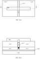
The sacrificial material layer 1019 may then be patterned to form a sacrificial gate. For example, as shown in the top view of FIG. 2(i) and the sectional view of 2(i′) (a sectional view taken along line AA′ in FIG. 2(i)), photoresist PR2 may be formed on the sacrificial material layer 1019. The photoresist PR2 may be formed in a shape corresponding to the sacrificial gate to be formed by photolithography (for example, exposure, development, etc.) Specifically, as shown in FIGS. 2(i) and 2(i′), the photoresist PR2 may be patterned into a bar shape extending in a direction (a horizontal direction in the figure) crossing (for example, perpendicular to) the fin F (defined by the spacer 1011). Then, as shown in FIG. 2(j), the sacrificial material layer 1019 may be selectively etched by, for example, RIE with the patterned photoresist PR2 as a mask. Thus, the sacrificial material layer 1019 constitutes a sacrificial gate, which has a bar shape extending in the direction crossing (for example, perpendicular to) the fin F as the patterned photoresist PR2.
After the fin F and the sacrificial gate 1019 are formed as described above, other elements of the device may be manufactured. For example, a gate spacer may be formed on sidewalls of the sacrificial gate, source/drain implantation (or strained source/drain may be formed by epitaxially growing a semiconductor layer) may be performed, or the like. It is well known to those skilled in the art to manufacture the FinFET using the replacement gate process, which will not be described in detail here.
The sacrificial gate may then be removed to form a final gate structure, comprising the first gate and the second gate.
Specifically, as shown in FIG. 2(k), a further dielectric layer 1031 (for example, oxide) may be formed on the isolation layer 1013. For example, oxide may be deposited on the structure shown in FIG. 2(j) and then planarized by, for example, CMP, to form the dielectric layer 1031. The CMP may stop at the sacrificial material layer 1019, to expose the sacrificial material layer 1019 for subsequent replacement thereof. As described above, as the sacrificial material layer 1019 has its top surface higher than that of the fin F, a portion of the spacer 1011 is remained on the top of the fin F after the CMP. The fin F and the spacer 1011 on top thereof divide the sacrificial material layer 1019 into two portions on the first side (for example, a left side in the figure) and the second side (for example, a right side in the figure) of the fin F.
Next, as shown in FIG. 2(l), the sacrificial material layer 1019 may be removed by selective etching (by, for example, a Tetramethylammonium hydroxide (TMAH) solution). Thus, a gate trench (which is in a space originally occupied by the sacrificial material layer 1019) (not shown) is left on the first side and the second side (the right side in the figure) of the fin F. A material stack for the gate may then be filled in the gate trench. For example, gate dielectric layers 1045-1/1045-2 and gate electrode layers 1047-1/1047-2 may be formed in sequence. For example, the gate dielectric layer may comprise a high-K gate dielectric such as HfO2 with a thickness of about 1-5 nm, and the gate electrode layer may comprise conductive metal such as W. For example, the gate dielectric layer may be deposited in a substantially conformal manner, and the gate electrode layer may be deposited to fill up the gate trench, and then planarization, for example, CMP may be performed (with the spacer 1011 as a stop point) to fill these layers in the gate trench. The interfacial layer may be reconstructed before the formation of the gate dielectric layer. In addition, a gate work function adjustment layer (not shown) may further be formed between the gate dielectric layer and the gate electrode layer.
Thus, the first gate (1045-1 and 1047-1) is formed on the first side of the fin F, and the second gate (1045-2 and 1047-2) is formed on the second side of the fin F, respectively. For example, one of the first gate and the second gate may act as a control gate and the other of the first gate and the second gate may act as a back gate.
Next, a metallization stack may be formed.
For example, as shown in FIG. 2(m), an interlayer dielectric layer 1049 (for example, oxide) may be formed on the structure shown in FIG. 2(l) by, for example, deposition. A contact 1051-1 may be formed at a position corresponding to the first gate. The contact may be formed, for example, by etching the interlayer dielectric layer to form a contact hole, and filling the contact hole with a conductive material layer (for example, W). Likewise, a contact may be formed at a position corresponding to a source/drain region (not shown). Certainly, it is also possible to firstly form a (conductive) diffusion barrier layer such as TiN on side and bottom walls of the contact hole, and then fill the contact hole with a conductive material.
A negative capacitor may be formed in the interlayer dielectric layer 1049.
For example, as shown in FIG. 2(n), photoresist PR3 may be formed on the interlayer dielectric layer 1049 having the contact formed therein. The photoresist PR3 may be patterned by photolithography to expose a portion of the interlayer dielectric layer 1049, where the negative capacitor is to be formed. Capacitance of the subsequently formed negative capacitor may be adjusted by adjusting a size of the portion exposed by the photoresist PR3. Then, the interlayer dielectric layer 1049 is selectively etched by, for example, RIE with the patterned photoresist PR3 as a mask, until the second gate (specifically, the gate electrode layer 1047-2 thereof) is exposed, thereby forming a trench R1 in the interlayer dielectric layer 1049. Here, the trench R1 is preferably biased to a side (i.e., the right side in the figure) opposite to the first gate. After that, the photoresist PR3 may be removed.
Subsequently, various material layers may be filled in the trench R1 to form the negative capacitor. For example, as shown in FIG. 2(o), a stack configuration of a first conductive layer-a negative capacitance material layer-a second conductive layer may be formed in sequence in the trench R1. In the example of FIG. 2(o), the first conductive layer may comprise a TiN layer 1033 (for example, with a thickness of about 1-5 nm, which may be formed by ALD). The TiN layer 1033, on one hand, acts as a plate of the negative capacitor due to its electrical conductivity, and on the other hand may also act as a diffusion barrier layer. The first conductive layer may also comprise one or more ohmic contact layers such as metal (for example, W or the like) of a low ohmic resistance, if desired (for example, to reduce contact resistance). The negative capacitance material layer may comprise an HfZrO2 layer 1035 (for example, with a thickness of about 2-100 nm, which may be formed by ALD). The second conductive layer may comprise a TiN layer 1037 (for example, with a thickness of about 1-5 nm, which may be formed by ALD) and an ohmic contact layer 1039 (for example, metal such as W, which may be formed by ALD or CVD), to act as another plate of the capacitor. Here, the TiN layer 1037 mainly acts as a diffusion barrier layer (which may be omitted), and the ohmic contact layer 1039 may be in contact with other contact components to be subsequently formed (for example, see 1055-2 shown in FIG. 2(q)). For example, the TiN layer 1033, the HfZrO2 layer 1035, and the TiN layer 1037 may be deposited in sequence in a substantially conformal manner, and the ohmic contact layer 1039 may be deposited to fill up the trench R1, and then planarization, for example, CMP, may be performed to fill the trench R1 with these layers.
In this example, one plate (1033) of the negative capacitor (1033, 1035, 1037 and 1039) is in direct contact with the gate electrode layer 1047-2 and is thus connected to the second gate.
Next, other layers in the metallization stack may be further formed. In this example, as metal interconnections (see FIG. 2(q)) are formed in an upper layer of the interlayer dielectric layer 1049, the TiN layer 1033, the HfZrO2 layer 1035, and the TiN layer 1037 may be etched back by selective etching such as RIE, so that they are recessed, as shown in FIG. 2(p). Subsequently, as shown in FIG. 2(q), another interlayer dielectric layer 1053 (for example, oxide) is formed on the interlayer dielectric layer 1049. Metal interconnections 1055-1 and 1055-2 corresponding to the contact 1051-1 and the ohmic contact layer 1039 may be formed in the interlayer dielectric layer 1053. The metal interconnections 1055-1 and 1055-2 each may extend in a certain route in the interlayer dielectric layer 1053 to electrically connect the contact 1051-1 and the ohmic contact layer 1039 (the other plate of the negative capacitor) to other components. As the TiN layer 1033, the HfZrO2 layer 1035 and the TiN layer 1037 are recessed and the recesses are filled with the interlayer dielectric layer 1053, unwanted electrical connections between these layers and the metal interconnection 1055-2 can be avoided.
In the above example, the trench R1 is biased to one side (the right side in the figure) of the second gate. Certainly, the present disclosure is not limited thereto. For example, the trench R1 may also be located directly above the second gate (the trench R1 may have a width less than that of the second gate). In addition, conductive vias may be formed in the interlayer dielectric layer 1053 (the metal interconnections may be formed in a further upper layer), and the conductive vias may be aligned with the contact 1051-1 and the gate electrode layer 1047-2, or the like, respectively. In this case, it is not necessary to recess the TiN layer 1033, the HfZrO2 layer 1035, and the TiN layer 1037 as described above. In addition, the negative capacitor may be formed on a further upper layer in the metallization stack and connected to the second gate through conductive via(s) and/or metal interconnection(s).
FIGS. 3(a)-3(m) are sectional views illustrating some of phases in a flow of manufacturing a FinFET according to another embodiment of the present disclosure.
As shown in FIG. 3(a), a substrate 2001 is provided. Here, an SOI substrate is described by way of example to exemplify an SOI FinFET. Specifically, the SOI substrate 2001 may comprise a base substrate 2001-1 (for example, silicon), a buried insulating layer 2001-2 (for example, oxide), and an SOI layer 2001-3 (for example, silicon).
An etching stop layer 2005 and an amorphous silicon layer 2007 may be formed in sequence on the substrate 2001. For the etching stop layer 2005 and the amorphous silicon layer 2007, reference can be made to the above description of the etching stop layer 1005 and the amorphous silicon layer 1007.
As shown in FIG. 3(b), the amorphous silicon layer 2007 may be patterned by, for example, RIE using patterned photoresist PR4 to form a sidewall extending in a first direction, which is at a position corresponding to one sidewall of a fin to be subsequently formed. The RIE may stop at the etching stop layer 2005. For this, reference can be made to the above description in conjunction with FIG. 2(b).
A hard mask for defining the fin may then be formed. For example, as shown in FIG. 3(c), a spacer 2011 may be formed on the sidewall of the patterned amorphous silicon layer 2007. For this, reference can be made to the above description in conjunction with FIG. 2(c).
After that, as shown in FIG. 3(d), the etching stop layer 2005 (if any) and the substrate 2001 (specifically, the SOI layer 2001-3) may be selectively etched by, for example, RIE, in sequence with the spacer 2011 as a mask to form the fin. Here, the etching of the substrate 2001 may stop at the buried insulating layer 2001-2.
Thus, relative to a portion of the substrate under the spacer 2011, remaining portions of the substrate may have their surfaces recessed, thereby forming a protruding fin F on the substrate 2001. Next, a gate intersecting the fin F may be formed on the substrate having the fin formed thereon. As this example is directed to the SOI substrate, it is not necessary to separately form an isolation layer.
As shown in FIG. 3(e), a sacrificial material layer 2019 may be formed on the buried insulating layer 2001-2. In addition, an interfacial layer 2017 may be formed on sidewalls of the fin F before the formation of the sacrificial material layer 2019. For this, reference can be made to the description above in connection with FIG. 2(h).
The sacrificial material layer 2019 may then be patterned to form a sacrificial gate.
To do this, as shown in the top view of FIG. 3(f) and the sectional view of FIG. 3(f) (a sectional view taken along line AA′ in FIG. 3(f)), photoresist PR5 may be formed on the sacrificial material layer 2019. The photoresist PR5 may be formed in a shape corresponding to the sacrificial gate to be formed by photolithography (for example, exposure, development, etc.) For this, reference can be made to the above description in connection with FIGS. 2(i) and 2(i′). Then, as shown in FIG. 3(g), the sacrificial material layer 2019 may be selectively etched by, for example, RIE with the patterned photoresist PR5 as a mask. The RIE may stop at the buried insulating layer 2001-2. Thus, the sacrificial material layer 2019 constitutes the sacrificial gate which has a bar shape extending in a direction crossing (for example, perpendicular to) the fin F.
After the fin F and the sacrificial gate are formed as described above, other elements of the device may be manufactured. After that, the sacrificial gate may be removed to form a final gate structure comprising a first gate and a second gate.
Specifically, as shown in FIG. 3(h), a further dielectric layer 2031 (for example, oxide) may be formed on the buried insulating layer 2001-2. Then, the sacrificial material layer 2019 is removed, and the first gate and the second gate are filled in spaces left on opposite sides of the fin F due to their removal, respectively. As shown in FIG. 3(i), the first gate may comprise a gate dielectric layer 2045-1 and a gate electrode layer 2047-1, and the second gate may comprise a gate dielectric layer 2045-2 and a gate electrode layer 2047-2. The first gate and the second gate may have substantially the same stack configuration. For this, reference can be made to the description above in connection with FIGS. 2(k) and 2(l).
Next, a metallization stack may be manufactured and a negative capacitor may be formed therein.
For example, as shown in FIG. 3(j), an interlayer dielectric layer 2049 (for example, oxide) may be formed on the structure shown in FIG. 3(i) by, for example, deposition. A contact 2051-1 may be formed at a position corresponding to the first gate. Further, as shown in FIG. 3(k), a trench R2 may be formed in the interlayer dielectric layer 2049 using patterned photoresist PR6. A negative capacitor may be formed by filling the trench R2 with various material layers. For example, as shown in FIG. 3(l), a stack configuration of a first conductive layer-a negative capacitance material layer-a second conductive layer may be formed in sequence in the trench R2. In the example of FIG. 3(l), the first conductive layer may comprise a TiN layer 2033 (for example, with a thickness of about 1-5 nm), the negative capacitance material layer may comprise a HfZrO2 layer 2035 (for example, with a thickness of about 2-100 nm), and the second conductive layer may comprise a TiN layer 2037 (for example, with a thickness of about 1-5 nm) and an ohmic contact layer 2039 (for example, metal such as W). After that, metal interconnections 2055-1 and 2055-2 may also be formed in another interlayer dielectric layer 2053 as shown in FIG. 3(m). For this, reference can be made to the above description in connection with FIGS. 2(m)-2(q).
The semiconductor devices according to the embodiments of the present disclosure are applicable to various electronic devices. For example, an Integrated Circuit (|C) may be formed by integrating a plurality of such semiconductor devices and other devices (for example, transistors in other forms etc.), from which an electronic device may be made. Therefore, the present disclosure further provides an electronic device comprising the above semiconductor device. The electronic device may also comprise components such as a display operatively coupled to the integrated circuit and a wireless transceiver operatively coupled to the integrated circuit, etc. Such an electronic device may comprise, for example, a smart phone, a tablet Personal Computer (PC), a Personal Digital Assistant (PDA), etc.
According to an embodiment of the present disclosure, there is also provided a method of manufacturing a System on Chip (SoC). The method may comprise the above method of manufacturing the semiconductor device. In particular, a number of various devices may be integrated on a chip, and at least some of the devices are manufactured by the method according to the present disclosure.
In the above descriptions, details of patterning and etching of the layers are not described. It is to be understood by those skilled in the art that various measures may be utilized to form the layers and regions in desired shapes. Further, to achieve the same feature, those skilled in the art can devise processes not entirely the same as those described above. The mere fact that the various embodiments are described separately does not mean that means recited in the respective embodiments cannot be used in combination to advantage.
The present disclosure is described above with reference to the embodiments thereof. However, those embodiments are provided only for illustrative purpose, rather than limiting the present disclosure. The scope of the disclosure is defined by the attached claims as well as equivalents thereof. Those skilled in the art can make various alternations and modifications without departing from the scope of the disclosure, which all fall within the scope of the disclosure.

Claims (8)

What is claimed is:
1. A method of manufacturing a Fin Field Effect Transistor (FinFET), comprising:
forming, on a substrate, a fin extending in a first direction;
forming, on the substrate, a first gate and a second gate opposite to the first gate extending in a second direction crossing the first direction respectively on a first side and a second side of the fin to intersect the fin;
providing a metallization stack on the substrate and above the fin and the first and second gates; and
forming, in the metallization stack, a negative capacitor connected to the second gate,
wherein the negative capacitor has a capacitance with an absolute value that is less than that of a second gate capacitor formed by the second gate.
2. The method according to claim 1, wherein forming the first gate and the second gate comprises:
forming, on the substrate, a sacrificial gate extending in the second direction to intersect the fin, wherein the sacrificial gate comprises a first portion on the first side of the fin and a second portion on the second side of the fin; and
removing the first portion and the second portion of the sacrificial gate, and forming the first gate and the second gate in spaces left due to the removal of the first portion and the second portion, respectively.
3. The method according to claim 2, wherein forming the fin comprises:
forming, on the substrate, a hard mask layer corresponding in shape to the fin to be formed; and
patterning the substrate using the hard mask layer to form the fin, and
wherein forming the sacrificial gate comprises:
forming a sacrificial material layer on the substrate having the fin formed thereon;
etching the sacrificial material layer back, so that the sacrificial material layer has a top surface higher than that of the fin but lower than that of the hard mask layer; and
patterning the sacrificial material layer into a shape extending in the second direction, so that a portion of the sacrificial material layer on the first side of the fin forms the first portion of the sacrificial gate and a portion of the sacrificial material layer on the second side of the fin forms the second portion of the sacrificial gate.
4. The method according to claim 3, wherein the hard mask layer is formed by a spacer process.
5. The method according to claim 3, wherein the sacrificial material layer is patterned using one same mask formed on the sacrificial material layer and extending in the second direction across the hard mask layer.
6. The method according to claim 3, wherein the substrate is a bulk semiconductor substrate, and after forming the fin and before forming the sacrificial material layer, the method further comprises:
forming an isolation layer on the substrate; and
performing ion implantation to form a punch-through stopper layer.
7. The method according to claim 3, wherein the substrate is a semiconductor-on-insulator (SOI) substrate, and the patterning of the substrate stops at a buried insulating layer of the SOI substrate.
8. The method according to claim 1, wherein forming the negative capacitor comprises:
forming a trench in an interlayer dielectric layer; and
sequentially forming a first conductive layer, a negative capacitance material layer, and a second conductive layer in the trench.
US17/005,097 2016-02-05 2020-08-27 Multi-gate FinFET including negative capacitor, method of manufacturing the same, and electronic device Active 2036-08-10 US11245035B2 (en)

Priority Applications (1)

Application Number Priority Date Filing Date Title
US17/005,097 US11245035B2 (en) 2016-02-05 2020-08-27 Multi-gate FinFET including negative capacitor, method of manufacturing the same, and electronic device

Applications Claiming Priority (5)

Application Number Priority Date Filing Date Title
CN201610082481.4 2016-02-05
CN201610082481.4A CN105702737B (en) 2016-02-05 2016-02-05 It is connected with the multiple-grid FinFET and its manufacturing method and electronic equipment of negative capacitance
PCT/CN2016/087249 WO2017133169A1 (en) 2016-02-05 2016-06-27 Finfet connected to negative capacitor, manufacturing method thereof and electronic device
US16/054,809 US10797178B2 (en) 2016-02-05 2018-08-03 Multi-gate FinFET including negative capacitor, method of manufacturing the same, and electronic device
US17/005,097 US11245035B2 (en) 2016-02-05 2020-08-27 Multi-gate FinFET including negative capacitor, method of manufacturing the same, and electronic device

Related Parent Applications (1)

Application Number Title Priority Date Filing Date
US16/054,809 Division US10797178B2 (en) 2016-02-05 2018-08-03 Multi-gate FinFET including negative capacitor, method of manufacturing the same, and electronic device

Publications (2)

Publication Number Publication Date
US20200395484A1 US20200395484A1 (en) 2020-12-17
US11245035B2 true US11245035B2 (en) 2022-02-08

Family

ID=56222029

Family Applications (3)

Application Number Title Priority Date Filing Date
US16/054,809 Active US10797178B2 (en) 2016-02-05 2018-08-03 Multi-gate FinFET including negative capacitor, method of manufacturing the same, and electronic device
US17/005,097 Active 2036-08-10 US11245035B2 (en) 2016-02-05 2020-08-27 Multi-gate FinFET including negative capacitor, method of manufacturing the same, and electronic device
US17/005,088 Active US11569388B2 (en) 2016-02-05 2020-08-27 Multi-gate FinFET including negative capacitor, method of manufacturing the same, and electronic device

Family Applications Before (1)

Application Number Title Priority Date Filing Date
US16/054,809 Active US10797178B2 (en) 2016-02-05 2018-08-03 Multi-gate FinFET including negative capacitor, method of manufacturing the same, and electronic device

Family Applications After (1)

Application Number Title Priority Date Filing Date
US17/005,088 Active US11569388B2 (en) 2016-02-05 2020-08-27 Multi-gate FinFET including negative capacitor, method of manufacturing the same, and electronic device

Country Status (3)

Country Link
US (3) US10797178B2 (en)
CN (1) CN105702737B (en)
WO (1) WO2017133169A1 (en)

Families Citing this family (6)

* Cited by examiner, † Cited by third party
Publication number Priority date Publication date Assignee Title
CN105702737B (en) 2016-02-05 2019-01-18 中国科学院微电子研究所 It is connected with the multiple-grid FinFET and its manufacturing method and electronic equipment of negative capacitance
US10861973B2 (en) 2018-06-27 2020-12-08 Taiwan Semiconductor Manufacturing Co., Ltd. Negative capacitance transistor with a diffusion blocking layer
CN110098251A (en) * 2019-04-15 2019-08-06 电子科技大学 A kind of novel I SFET device and preparation method thereof
US11164867B2 (en) * 2019-08-07 2021-11-02 Globalfoundries U.S. Inc. Fin-type field-effect transistors over one or more buried polycrystalline layers
CN113571418B (en) * 2021-05-31 2024-03-08 上海华力集成电路制造有限公司 Super well forming method of FinFET
US11916099B2 (en) 2021-06-08 2024-02-27 International Business Machines Corporation Multilayer dielectric for metal-insulator-metal capacitor

Citations (42)

* Cited by examiner, † Cited by third party
Publication number Priority date Publication date Assignee Title
US20050167725A1 (en) * 2004-01-29 2005-08-04 Matsushita Electric Industrial Co., Ltd. Capacitor element and method for fabricating the same
US20050266645A1 (en) * 2004-05-25 2005-12-01 Jin-Jun Park Phosphorous doping methods of manufacturing field effect transistors having multiple stacked channels
US20060084232A1 (en) * 2002-08-12 2006-04-20 Grupp Daniel E Process for fabricating a self-aligned deposited source/drain insulated gate field-effect transistor
US20060108621A1 (en) 2004-11-24 2006-05-25 Matsushita Electric Industrial Co., Ltd. Capacitor insulating film, method for fabricating the same, capacitor element, method for fabricating the same, semiconductor memory device, and method for fabricating the same
US20070004049A1 (en) 2005-06-30 2007-01-04 Hayato Nasu Semiconductor device having ferroelectric film as gate insulating film and manufacturing method thereof
CN101207155A (en) 2006-12-22 2008-06-25 英特尔公司 Floating body memory cell having gates favoring different conductivity type regions
US20090127625A1 (en) 2007-11-21 2009-05-21 Kabushiki Kaisha Toshiba Semiconductor device
US20120091538A1 (en) * 2010-10-13 2012-04-19 Taiwan Semiconductor Manufacturing Company, Ltd. Finfet and method of fabricating the same
US20120139028A1 (en) 2010-12-01 2012-06-07 Samsung Electronics Co., Ltd. Semiconductor memory device and emthod of forming the same
US20120175696A1 (en) 2010-11-09 2012-07-12 North Carolina State University Multilayer floating gate field-effect transistor (fet) devices and related methods
US20120181605A1 (en) * 2008-06-02 2012-07-19 Micron Technology, Inc. Methods of providing electrical isolation and semiconductor structures including same
US20120217559A1 (en) 2011-02-28 2012-08-30 Samsung Electronics Co., Ltd. Semiconductor memory device
US20130264630A1 (en) * 2012-04-09 2013-10-10 Samsung Electronics Co., Ltd. Semiconductor devices having transistors capable of adjusting threshold voltage through body bias effect
US20140106523A1 (en) 2012-10-12 2014-04-17 Viktor Koldiaev Vertical Super-Thin Body Semiconductor on Dielectric Wall Devices and Methods of Their Fabrication
CN104112748A (en) 2013-04-19 2014-10-22 中国科学院微电子研究所 Memory device, manufacturing method and access method of memory device
US20140319623A1 (en) 2011-12-28 2014-10-30 Curtis Tsai Methods of integrating multiple gate dielectric transistors on a tri-gate (finfet) process
US20150194422A1 (en) * 2014-01-06 2015-07-09 Taiwan Semiconductor Manufacturing Company Limited Semiconductor arrangement and formation thereof
US20150221770A1 (en) 2013-08-01 2015-08-06 Globalfoundries Inc. Epitaxially forming a set of fins in a semiconductor device
US20150228544A1 (en) 2013-03-11 2015-08-13 Taiwan Semiconductor Manufacturing Company, Ltd. Fin Shape For Fin Field-Effect Transistors And Method Of Forming
US20150294969A1 (en) 2014-04-15 2015-10-15 Samsung Electronics Co., Ltd. Finfet-based semiconductor device with dummy gates
US20150303277A1 (en) * 2014-04-17 2015-10-22 International Business Machines Corporation Gate to Diffusion Local Interconnect Scheme Using Selective Replacement Gate Flow
US20150311349A1 (en) * 2014-04-24 2015-10-29 Micron Technology, Inc. Ferroelectric Field Effect Transistors, Pluralities Of Ferroelectric Field Effect Transistors Arrayed In Row Lines And Column Lines, And Methods Of Forming A Plurality Of Ferroelectric Field Effect Transistors
US20150318285A1 (en) 2014-04-30 2015-11-05 Stmicroelectronics, Inc. Dram interconnect structure having ferroelectric capacitors
US20150333072A1 (en) * 2014-05-16 2015-11-19 Qualcomm Incorporated Advanced metal-nitride-oxide-silicon multiple-time programmable memory
US20150380504A1 (en) 2012-11-26 2015-12-31 Ps5 Luxco S.A.R.L. Device and method for manufacturing same
US20160049486A1 (en) 2014-08-15 2016-02-18 Infineon Technologies Austria Ag Semiconductor Device Having a Tapered Gate Structure and Method
US20160141417A1 (en) 2014-11-19 2016-05-19 Samsung Electronics Co., Ltd. Semiconductor device and method for fabricating the same
US20160141366A1 (en) * 2014-11-17 2016-05-19 National Taiwan University Field Effect Transistors and Methods of Forming Same
US20160155748A1 (en) 2014-12-01 2016-06-02 Qualcomm Incorporated High dielectric constant/metal gate (hk/mg) compatible floating gate (fg)/ferroelectric dipole non-volatile memory and logic device
US20160155843A1 (en) 2013-12-16 2016-06-02 Intel Corporation Multi-threshold voltage devices and associated techniques and configurations
CN105702737A (en) 2016-02-05 2016-06-22 中国科学院微电子研究所 Multi-grid FinFET connected with negative capacitor, manufacture method therefor and electronic device
US20160322503A1 (en) 2015-04-28 2016-11-03 Semiconductor Energy Laboratory Co., Ltd. Semiconductor device and manufacturing method thereof
US20160336312A1 (en) 2015-05-15 2016-11-17 Taiwan Semiconductor Manufacturing Company Limited Semiconductor device and transistor
US20170004975A1 (en) 2013-12-27 2017-01-05 Intel Corporation Technologies for selectively etching oxide and nitride materials and products formed using the same
US20170040172A1 (en) 2015-08-04 2017-02-09 Samsung Electronics Co., Ltd. Methods of forming material layer
US20170084741A1 (en) 2015-09-18 2017-03-23 Taiwan Semiconductor Manufacturing Co., Ltd. Enhanced channel strain to reduce contact resistance in nmos fet devices
US20170092638A1 (en) 2015-09-30 2017-03-30 Samsung Electronics Co., Ltd. Semiconductor device
US20170346477A1 (en) * 2016-05-24 2017-11-30 Maxim Integrated Products, Inc. LDMOS Transistors And Associated Systems And Methods
US20180053830A1 (en) 2016-08-19 2018-02-22 International Business Machines Corporation Semiconductor device including enhanced low-k spacer
US20180076334A1 (en) 2016-09-13 2018-03-15 International Business Machines Corporation Integrated ferroelectric capacitor/ field effect transistor structure
US20180151745A1 (en) 2016-11-29 2018-05-31 Taiwan Semiconductor Manufacturing Co., Ltd. Semiconductor device and manufacturing method thereof
US20200066867A1 (en) * 2018-08-22 2020-02-27 International Business Machines Corporation Fully depleted soi transistor with a buried ferroelectric layer in back-gate

Patent Citations (66)

* Cited by examiner, † Cited by third party
Publication number Priority date Publication date Assignee Title
US20060084232A1 (en) * 2002-08-12 2006-04-20 Grupp Daniel E Process for fabricating a self-aligned deposited source/drain insulated gate field-effect transistor
US20050167725A1 (en) * 2004-01-29 2005-08-04 Matsushita Electric Industrial Co., Ltd. Capacitor element and method for fabricating the same
US20050266645A1 (en) * 2004-05-25 2005-12-01 Jin-Jun Park Phosphorous doping methods of manufacturing field effect transistors having multiple stacked channels
US20090321801A1 (en) 2004-11-24 2009-12-31 Panasonic Corporation Capacitor insulating film, method for fabricating the same, capacitor element, method for fabricating the same, semiconductor memory device, and method for fabricating the same
US20060108621A1 (en) 2004-11-24 2006-05-25 Matsushita Electric Industrial Co., Ltd. Capacitor insulating film, method for fabricating the same, capacitor element, method for fabricating the same, semiconductor memory device, and method for fabricating the same
CN1779976A (en) 2004-11-24 2006-05-31 松下电器产业株式会社 Capacitor insulating film, method for fabricating the same, capacitor element, method for fabricating the same, semiconductor memory device, and method for fabricating the same
US20070004049A1 (en) 2005-06-30 2007-01-04 Hayato Nasu Semiconductor device having ferroelectric film as gate insulating film and manufacturing method thereof
CN1893114A (en) 2005-06-30 2007-01-10 株式会社东芝 Semiconductor device having ferroelectric film as gate insulating film and manufacturing method thereof
US20140015021A1 (en) 2006-12-22 2014-01-16 Peter L. D. Chang Floating body memory cell having gates favoring different conductivity type regions
US20150179650A1 (en) 2006-12-22 2015-06-25 Peter L. D. Chang Floating body memory cell having gates favoring different conductivity type regions
US20080149984A1 (en) 2006-12-22 2008-06-26 Chang Peter L D Floating body memory cell having gates favoring different conductivity type regions
US20160322360A1 (en) 2006-12-22 2016-11-03 Peter L. D. Chang Floating body memory cell having gates favoring different conductivity type regions
US20160155742A1 (en) 2006-12-22 2016-06-02 Peter L. D. Chang Floating body memory cell having gates favoring different conductivity type regions
US8217435B2 (en) 2006-12-22 2012-07-10 Intel Corporation Floating body memory cell having gates favoring different conductivity type regions
US9520399B2 (en) 2006-12-22 2016-12-13 Intel Corporation Floating body memory cell having gates favoring different conductivity type regions
CN101207155A (en) 2006-12-22 2008-06-25 英特尔公司 Floating body memory cell having gates favoring different conductivity type regions
US9275999B2 (en) 2006-12-22 2016-03-01 Intel Corporation Floating body memory cell having gates favoring different conductivity type regions
US20120267721A1 (en) 2006-12-22 2012-10-25 Chang Peter L D Floating body memory cell having gates favoring different conductivity type regions
US20170062434A1 (en) 2006-12-22 2017-03-02 Peter L. D. Chang Floating body memory cell having gates favoring different conductivity type regions
US8569812B2 (en) 2006-12-22 2013-10-29 Intel Corporation Floating body memory cell having gates favoring different conductivity type regions
US9418997B2 (en) 2006-12-22 2016-08-16 Intel Corporation Floating body memory cell having gates favoring different conductivity type regions
US9646970B2 (en) 2006-12-22 2017-05-09 Intel Corporation Floating body memory cell having gates favoring different conductivity type regions
US20170207222A1 (en) 2006-12-22 2017-07-20 Intel Corporation Floating body memory cell having gates favoring different conductivity type regions
US9786667B2 (en) 2006-12-22 2017-10-10 Intel Corporation Floating body memory cell having gates favoring different conductivity type regions
US8980707B2 (en) 2006-12-22 2015-03-17 Intel Corporation Floating body memory cell having gates favoring different conductivity type regions
US20180226407A1 (en) 2006-12-22 2018-08-09 Intel Corporation Floating body memory cell having gates favoring different conductivity type regions
US20190035790A1 (en) 2006-12-22 2019-01-31 Intel Corporation Floating body memory cell having gates favoring different conductivity type regions
US10121792B2 (en) 2006-12-22 2018-11-06 Intel Corporation Floating body memory cell having gates favoring different conductivity type regions
US20090127625A1 (en) 2007-11-21 2009-05-21 Kabushiki Kaisha Toshiba Semiconductor device
US20120181605A1 (en) * 2008-06-02 2012-07-19 Micron Technology, Inc. Methods of providing electrical isolation and semiconductor structures including same
US20120091538A1 (en) * 2010-10-13 2012-04-19 Taiwan Semiconductor Manufacturing Company, Ltd. Finfet and method of fabricating the same
US20120175696A1 (en) 2010-11-09 2012-07-12 North Carolina State University Multilayer floating gate field-effect transistor (fet) devices and related methods
US20120139028A1 (en) 2010-12-01 2012-06-07 Samsung Electronics Co., Ltd. Semiconductor memory device and emthod of forming the same
US20120217559A1 (en) 2011-02-28 2012-08-30 Samsung Electronics Co., Ltd. Semiconductor memory device
US20140319623A1 (en) 2011-12-28 2014-10-30 Curtis Tsai Methods of integrating multiple gate dielectric transistors on a tri-gate (finfet) process
US20130264630A1 (en) * 2012-04-09 2013-10-10 Samsung Electronics Co., Ltd. Semiconductor devices having transistors capable of adjusting threshold voltage through body bias effect
US20140106523A1 (en) 2012-10-12 2014-04-17 Viktor Koldiaev Vertical Super-Thin Body Semiconductor on Dielectric Wall Devices and Methods of Their Fabrication
US20150380504A1 (en) 2012-11-26 2015-12-31 Ps5 Luxco S.A.R.L. Device and method for manufacturing same
US20150228544A1 (en) 2013-03-11 2015-08-13 Taiwan Semiconductor Manufacturing Company, Ltd. Fin Shape For Fin Field-Effect Transistors And Method Of Forming
CN104112748A (en) 2013-04-19 2014-10-22 中国科学院微电子研究所 Memory device, manufacturing method and access method of memory device
US20150221770A1 (en) 2013-08-01 2015-08-06 Globalfoundries Inc. Epitaxially forming a set of fins in a semiconductor device
US20160155843A1 (en) 2013-12-16 2016-06-02 Intel Corporation Multi-threshold voltage devices and associated techniques and configurations
US20170004975A1 (en) 2013-12-27 2017-01-05 Intel Corporation Technologies for selectively etching oxide and nitride materials and products formed using the same
US20150194422A1 (en) * 2014-01-06 2015-07-09 Taiwan Semiconductor Manufacturing Company Limited Semiconductor arrangement and formation thereof
US20150294969A1 (en) 2014-04-15 2015-10-15 Samsung Electronics Co., Ltd. Finfet-based semiconductor device with dummy gates
US20150303277A1 (en) * 2014-04-17 2015-10-22 International Business Machines Corporation Gate to Diffusion Local Interconnect Scheme Using Selective Replacement Gate Flow
US20150311349A1 (en) * 2014-04-24 2015-10-29 Micron Technology, Inc. Ferroelectric Field Effect Transistors, Pluralities Of Ferroelectric Field Effect Transistors Arrayed In Row Lines And Column Lines, And Methods Of Forming A Plurality Of Ferroelectric Field Effect Transistors
US20150318285A1 (en) 2014-04-30 2015-11-05 Stmicroelectronics, Inc. Dram interconnect structure having ferroelectric capacitors
US20150333072A1 (en) * 2014-05-16 2015-11-19 Qualcomm Incorporated Advanced metal-nitride-oxide-silicon multiple-time programmable memory
US20160049486A1 (en) 2014-08-15 2016-02-18 Infineon Technologies Austria Ag Semiconductor Device Having a Tapered Gate Structure and Method
US20160141366A1 (en) * 2014-11-17 2016-05-19 National Taiwan University Field Effect Transistors and Methods of Forming Same
US20160141417A1 (en) 2014-11-19 2016-05-19 Samsung Electronics Co., Ltd. Semiconductor device and method for fabricating the same
US20160155748A1 (en) 2014-12-01 2016-06-02 Qualcomm Incorporated High dielectric constant/metal gate (hk/mg) compatible floating gate (fg)/ferroelectric dipole non-volatile memory and logic device
US20160322503A1 (en) 2015-04-28 2016-11-03 Semiconductor Energy Laboratory Co., Ltd. Semiconductor device and manufacturing method thereof
US20160336312A1 (en) 2015-05-15 2016-11-17 Taiwan Semiconductor Manufacturing Company Limited Semiconductor device and transistor
US20170040172A1 (en) 2015-08-04 2017-02-09 Samsung Electronics Co., Ltd. Methods of forming material layer
US20170084741A1 (en) 2015-09-18 2017-03-23 Taiwan Semiconductor Manufacturing Co., Ltd. Enhanced channel strain to reduce contact resistance in nmos fet devices
US20170092638A1 (en) 2015-09-30 2017-03-30 Samsung Electronics Co., Ltd. Semiconductor device
CN105702737A (en) 2016-02-05 2016-06-22 中国科学院微电子研究所 Multi-grid FinFET connected with negative capacitor, manufacture method therefor and electronic device
US20180342622A1 (en) 2016-02-05 2018-11-29 Institute of Microelectronics, Chinese Academy of Sciences Multi-gate finfet including negative capacitor, method of manufacturing the same, and electronic device
US10797178B2 (en) 2016-02-05 2020-10-06 Institute of Microelectronics Chinese Academy of Sciences Multi-gate FinFET including negative capacitor, method of manufacturing the same, and electronic device
US20170346477A1 (en) * 2016-05-24 2017-11-30 Maxim Integrated Products, Inc. LDMOS Transistors And Associated Systems And Methods
US20180053830A1 (en) 2016-08-19 2018-02-22 International Business Machines Corporation Semiconductor device including enhanced low-k spacer
US20180076334A1 (en) 2016-09-13 2018-03-15 International Business Machines Corporation Integrated ferroelectric capacitor/ field effect transistor structure
US20180151745A1 (en) 2016-11-29 2018-05-31 Taiwan Semiconductor Manufacturing Co., Ltd. Semiconductor device and manufacturing method thereof
US20200066867A1 (en) * 2018-08-22 2020-02-27 International Business Machines Corporation Fully depleted soi transistor with a buried ferroelectric layer in back-gate

Non-Patent Citations (5)

* Cited by examiner, † Cited by third party
Title
International Search Report and Written Opinion with Translation for International Application No. PCT/CN2016/087249 dated Nov. 10, 2016, which corresponds in priority to above-identified subject U.S. Application.
International Search Report for International Application No. PCT/CN2016/087249 dated Nov. 10, 2016.
Khan et al. "Negative Capacitance in Short-Channel FinFETs Externally Connected to an Epitaxial Ferroelectric Capacitor" IEEE Electron Device Letters, vol. 37, No. 1, Jan. 2016.
Negative Capacitance in Short-Channel FinFETs Externally Connected to an Epitaxial Ferroelectric Capacitor, IEEE Electron Device Letters, vol. 37, No. 1, pp. 111-114, Nov. 18, 2015 (Year: 2015).
Office Action with Translation for Chinese Application No. 201610082481.4 dated Feb. 24, 2018, which corresponds in priority to above-identified subject U.S. Application.

Also Published As

Publication number Publication date
US11569388B2 (en) 2023-01-31
US20180342622A1 (en) 2018-11-29
US10797178B2 (en) 2020-10-06
CN105702737A (en) 2016-06-22
CN105702737B (en) 2019-01-18
WO2017133169A1 (en) 2017-08-10
US20200395483A1 (en) 2020-12-17
US20200395484A1 (en) 2020-12-17

Similar Documents

Publication Publication Date Title
US11245035B2 (en) Multi-gate FinFET including negative capacitor, method of manufacturing the same, and electronic device
US10242990B2 (en) Structure featuring ferroelectric capacitance in interconnect level for steep sub-threshold complementary metal oxide semiconductor transistors
TWI556427B (en) Buffer layer on gate and methods of forming the same
US10497809B2 (en) FINFET, method of manufacturing the same, and electronic device including the same
US11031298B2 (en) Semiconductor device and method
US8610249B2 (en) Non-planar capacitor and method of forming the non-planar capacitor
US11515332B2 (en) Ferroelectric memory device and method of forming the same
US11647635B2 (en) Ferroelectric memory device and method of forming the same
CN111048588A (en) Semiconductor device, method of manufacturing the same, and electronic apparatus including the same
US20220367515A1 (en) Ferroelectric memory device and method of forming the same
CN111373538B (en) Three-dimensional memory device and method of fabricating the same
US11950427B2 (en) Ferroelectric memory device and method of forming the same
US20220310445A1 (en) Transistor Gate Contacts and Methods of Forming the Same
US11842933B2 (en) Semiconductor device and method
US11804408B2 (en) Semiconductor device and method
US11727976B2 (en) Semiconductor devices including ferroelectric memory and methods of forming the same
US20220392889A1 (en) Capacitor structure for semiconductor device and method
CN215527730U (en) Memory device
US20230033289A1 (en) Gate structures in transistor devices and methods of forming same
US11974441B2 (en) Memory array including epitaxial source lines and bit lines
US20230028653A1 (en) Semiconductor Device and Method of Forming Same
CN114121959A (en) Memory device, method of manufacturing the same, and electronic apparatus including the same

Legal Events

Date Code Title Description
FEPP Fee payment procedure

Free format text: ENTITY STATUS SET TO UNDISCOUNTED (ORIGINAL EVENT CODE: BIG.); ENTITY STATUS OF PATENT OWNER: SMALL ENTITY

FEPP Fee payment procedure

Free format text: ENTITY STATUS SET TO SMALL (ORIGINAL EVENT CODE: SMAL); ENTITY STATUS OF PATENT OWNER: SMALL ENTITY

STPP Information on status: patent application and granting procedure in general

Free format text: DOCKETED NEW CASE - READY FOR EXAMINATION

STPP Information on status: patent application and granting procedure in general

Free format text: NOTICE OF ALLOWANCE MAILED -- APPLICATION RECEIVED IN OFFICE OF PUBLICATIONS

STPP Information on status: patent application and granting procedure in general

Free format text: PUBLICATIONS -- ISSUE FEE PAYMENT RECEIVED

STPP Information on status: patent application and granting procedure in general

Free format text: PUBLICATIONS -- ISSUE FEE PAYMENT VERIFIED

STCF Information on status: patent grant

Free format text: PATENTED CASE