WO2017111174A1 - 積層体 - Google Patents
積層体 Download PDFInfo
- Publication number
- WO2017111174A1 WO2017111174A1 PCT/JP2016/088765 JP2016088765W WO2017111174A1 WO 2017111174 A1 WO2017111174 A1 WO 2017111174A1 JP 2016088765 W JP2016088765 W JP 2016088765W WO 2017111174 A1 WO2017111174 A1 WO 2017111174A1
- Authority
- WO
- WIPO (PCT)
- Prior art keywords
- layer
- substrate
- oxide semiconductor
- metal oxide
- electrode layer
- Prior art date
Links
- 239000004065 semiconductor Substances 0.000 claims abstract description 142
- 239000000758 substrate Substances 0.000 claims abstract description 137
- 229910044991 metal oxide Inorganic materials 0.000 claims abstract description 76
- 150000004706 metal oxides Chemical class 0.000 claims abstract description 76
- 230000009467 reduction Effects 0.000 claims abstract description 65
- 229910052751 metal Inorganic materials 0.000 claims description 42
- 239000002184 metal Substances 0.000 claims description 42
- 230000004888 barrier function Effects 0.000 claims description 26
- 230000001629 suppression Effects 0.000 claims description 22
- 229910052721 tungsten Inorganic materials 0.000 claims description 17
- 229910052759 nickel Inorganic materials 0.000 claims description 13
- 125000004435 hydrogen atom Chemical group [H]* 0.000 claims description 12
- 229910052710 silicon Inorganic materials 0.000 claims description 12
- XUIMIQQOPSSXEZ-UHFFFAOYSA-N Silicon Chemical compound [Si] XUIMIQQOPSSXEZ-UHFFFAOYSA-N 0.000 claims description 11
- 239000010703 silicon Substances 0.000 claims description 11
- 150000002739 metals Chemical class 0.000 claims description 10
- 229910052719 titanium Inorganic materials 0.000 claims description 10
- 229910052738 indium Inorganic materials 0.000 claims description 9
- 229910052804 chromium Inorganic materials 0.000 claims description 8
- 229910052782 aluminium Inorganic materials 0.000 claims description 7
- 229910052741 iridium Inorganic materials 0.000 claims description 7
- 229910052750 molybdenum Inorganic materials 0.000 claims description 7
- 229910052763 palladium Inorganic materials 0.000 claims description 7
- 229910052702 rhenium Inorganic materials 0.000 claims description 7
- 229910052703 rhodium Inorganic materials 0.000 claims description 7
- 229910052748 manganese Inorganic materials 0.000 claims description 6
- 229910052709 silver Inorganic materials 0.000 claims description 6
- 229910052733 gallium Inorganic materials 0.000 claims description 5
- 229910052725 zinc Inorganic materials 0.000 claims description 5
- 229910052707 ruthenium Inorganic materials 0.000 claims description 4
- 229910021332 silicide Inorganic materials 0.000 claims description 4
- 229910052718 tin Inorganic materials 0.000 claims description 4
- 125000004429 atom Chemical group 0.000 claims description 3
- FVBUAEGBCNSCDD-UHFFFAOYSA-N silicide(4-) Chemical compound [Si-4] FVBUAEGBCNSCDD-UHFFFAOYSA-N 0.000 claims description 3
- 239000010410 layer Substances 0.000 description 376
- 239000010408 film Substances 0.000 description 45
- 238000000034 method Methods 0.000 description 29
- WGTYBPLFGIVFAS-UHFFFAOYSA-M tetramethylammonium hydroxide Chemical compound [OH-].C[N+](C)(C)C WGTYBPLFGIVFAS-UHFFFAOYSA-M 0.000 description 18
- 230000015572 biosynthetic process Effects 0.000 description 15
- KDLHZDBZIXYQEI-UHFFFAOYSA-N palladium Substances [Pd] KDLHZDBZIXYQEI-UHFFFAOYSA-N 0.000 description 15
- 238000005259 measurement Methods 0.000 description 12
- HBEQXAKJSGXAIQ-UHFFFAOYSA-N oxopalladium Chemical compound [Pd]=O HBEQXAKJSGXAIQ-UHFFFAOYSA-N 0.000 description 10
- 229910003445 palladium oxide Inorganic materials 0.000 description 10
- 229910045601 alloy Inorganic materials 0.000 description 9
- 239000000956 alloy Substances 0.000 description 9
- 239000000463 material Substances 0.000 description 9
- XLOMVQKBTHCTTD-UHFFFAOYSA-N Zinc monoxide Chemical compound [Zn]=O XLOMVQKBTHCTTD-UHFFFAOYSA-N 0.000 description 8
- 238000005229 chemical vapour deposition Methods 0.000 description 8
- 230000006870 function Effects 0.000 description 8
- 229910052760 oxygen Inorganic materials 0.000 description 8
- 239000011701 zinc Substances 0.000 description 8
- 239000007789 gas Substances 0.000 description 7
- 238000004519 manufacturing process Methods 0.000 description 7
- BASFCYQUMIYNBI-UHFFFAOYSA-N platinum Substances [Pt] BASFCYQUMIYNBI-UHFFFAOYSA-N 0.000 description 7
- 230000008569 process Effects 0.000 description 7
- 230000003746 surface roughness Effects 0.000 description 7
- 239000013078 crystal Substances 0.000 description 6
- HTXDPTMKBJXEOW-UHFFFAOYSA-N dioxoiridium Chemical compound O=[Ir]=O HTXDPTMKBJXEOW-UHFFFAOYSA-N 0.000 description 6
- 229910000457 iridium oxide Inorganic materials 0.000 description 6
- 229910001925 ruthenium oxide Inorganic materials 0.000 description 6
- WOCIAKWEIIZHES-UHFFFAOYSA-N ruthenium(iv) oxide Chemical compound O=[Ru]=O WOCIAKWEIIZHES-UHFFFAOYSA-N 0.000 description 6
- 229910005191 Ga 2 O 3 Inorganic materials 0.000 description 5
- 229910052758 niobium Inorganic materials 0.000 description 5
- 238000004544 sputter deposition Methods 0.000 description 5
- CSCPPACGZOOCGX-UHFFFAOYSA-N Acetone Chemical compound CC(C)=O CSCPPACGZOOCGX-UHFFFAOYSA-N 0.000 description 4
- 239000004642 Polyimide Substances 0.000 description 4
- VYPSYNLAJGMNEJ-UHFFFAOYSA-N Silicium dioxide Chemical compound O=[Si]=O VYPSYNLAJGMNEJ-UHFFFAOYSA-N 0.000 description 4
- 238000003917 TEM image Methods 0.000 description 4
- QVGXLLKOCUKJST-UHFFFAOYSA-N atomic oxygen Chemical compound [O] QVGXLLKOCUKJST-UHFFFAOYSA-N 0.000 description 4
- 230000015556 catabolic process Effects 0.000 description 4
- 230000005684 electric field Effects 0.000 description 4
- 229910052737 gold Inorganic materials 0.000 description 4
- 150000002500 ions Chemical group 0.000 description 4
- 239000000203 mixture Substances 0.000 description 4
- MUMZUERVLWJKNR-UHFFFAOYSA-N oxoplatinum Chemical compound [Pt]=O MUMZUERVLWJKNR-UHFFFAOYSA-N 0.000 description 4
- 239000001301 oxygen Substances 0.000 description 4
- 229910003446 platinum oxide Inorganic materials 0.000 description 4
- 229920001721 polyimide Polymers 0.000 description 4
- 238000005036 potential barrier Methods 0.000 description 4
- 229920001187 thermosetting polymer Polymers 0.000 description 4
- 239000011787 zinc oxide Substances 0.000 description 4
- 229910052726 zirconium Inorganic materials 0.000 description 4
- 229910018072 Al 2 O 3 Inorganic materials 0.000 description 3
- 238000010521 absorption reaction Methods 0.000 description 3
- 238000006243 chemical reaction Methods 0.000 description 3
- 229910052802 copper Inorganic materials 0.000 description 3
- 238000002149 energy-dispersive X-ray emission spectroscopy Methods 0.000 description 3
- 238000005516 engineering process Methods 0.000 description 3
- 238000011156 evaluation Methods 0.000 description 3
- 230000005669 field effect Effects 0.000 description 3
- 239000001257 hydrogen Substances 0.000 description 3
- 229910052739 hydrogen Inorganic materials 0.000 description 3
- 238000002347 injection Methods 0.000 description 3
- 239000007924 injection Substances 0.000 description 3
- 230000015654 memory Effects 0.000 description 3
- 238000000059 patterning Methods 0.000 description 3
- 230000001681 protective effect Effects 0.000 description 3
- 239000000523 sample Substances 0.000 description 3
- WSMQKESQZFQMFW-UHFFFAOYSA-N 5-methyl-pyrazole-3-carboxylic acid Chemical compound CC1=CC(C(O)=O)=NN1 WSMQKESQZFQMFW-UHFFFAOYSA-N 0.000 description 2
- 229910005542 GaSb Inorganic materials 0.000 description 2
- 229910001218 Gallium arsenide Inorganic materials 0.000 description 2
- 230000005355 Hall effect Effects 0.000 description 2
- UFHFLCQGNIYNRP-UHFFFAOYSA-N Hydrogen Chemical compound [H][H] UFHFLCQGNIYNRP-UHFFFAOYSA-N 0.000 description 2
- 229910000673 Indium arsenide Inorganic materials 0.000 description 2
- 229910021193 La 2 O 3 Inorganic materials 0.000 description 2
- 229910052581 Si3N4 Inorganic materials 0.000 description 2
- 229910007709 ZnTe Inorganic materials 0.000 description 2
- 230000005540 biological transmission Effects 0.000 description 2
- 230000000903 blocking effect Effects 0.000 description 2
- 239000000919 ceramic Substances 0.000 description 2
- 230000000052 comparative effect Effects 0.000 description 2
- 238000000151 deposition Methods 0.000 description 2
- 239000010432 diamond Substances 0.000 description 2
- 229910003460 diamond Inorganic materials 0.000 description 2
- 230000000694 effects Effects 0.000 description 2
- 239000012776 electronic material Substances 0.000 description 2
- 239000011521 glass Substances 0.000 description 2
- 230000005525 hole transport Effects 0.000 description 2
- WPYVAWXEWQSOGY-UHFFFAOYSA-N indium antimonide Chemical compound [Sb]#[In] WPYVAWXEWQSOGY-UHFFFAOYSA-N 0.000 description 2
- RPQDHPTXJYYUPQ-UHFFFAOYSA-N indium arsenide Chemical compound [In]#[As] RPQDHPTXJYYUPQ-UHFFFAOYSA-N 0.000 description 2
- 239000011229 interlayer Substances 0.000 description 2
- 229910052746 lanthanum Inorganic materials 0.000 description 2
- 229910052745 lead Inorganic materials 0.000 description 2
- GQYHUHYESMUTHG-UHFFFAOYSA-N lithium niobate Chemical compound [Li+].[O-][Nb](=O)=O GQYHUHYESMUTHG-UHFFFAOYSA-N 0.000 description 2
- 239000010453 quartz Substances 0.000 description 2
- 230000004044 response Effects 0.000 description 2
- 229910052594 sapphire Inorganic materials 0.000 description 2
- 239000010980 sapphire Substances 0.000 description 2
- 238000001004 secondary ion mass spectrometry Methods 0.000 description 2
- HQVNEWCFYHHQES-UHFFFAOYSA-N silicon nitride Chemical compound N12[Si]34N5[Si]62N3[Si]51N64 HQVNEWCFYHHQES-UHFFFAOYSA-N 0.000 description 2
- 229910052814 silicon oxide Inorganic materials 0.000 description 2
- 239000002356 single layer Substances 0.000 description 2
- 238000001228 spectrum Methods 0.000 description 2
- 238000003860 storage Methods 0.000 description 2
- 239000010409 thin film Substances 0.000 description 2
- 229910002704 AlGaN Inorganic materials 0.000 description 1
- JMASRVWKEDWRBT-UHFFFAOYSA-N Gallium nitride Chemical compound [Ga]#N JMASRVWKEDWRBT-UHFFFAOYSA-N 0.000 description 1
- 229910004129 HfSiO Inorganic materials 0.000 description 1
- 229910052779 Neodymium Inorganic materials 0.000 description 1
- 238000006124 Pilkington process Methods 0.000 description 1
- 229910004205 SiNX Inorganic materials 0.000 description 1
- 229910004298 SiO 2 Inorganic materials 0.000 description 1
- 229910007541 Zn O Inorganic materials 0.000 description 1
- 230000009471 action Effects 0.000 description 1
- 239000000443 aerosol Substances 0.000 description 1
- 239000005407 aluminoborosilicate glass Substances 0.000 description 1
- 239000005354 aluminosilicate glass Substances 0.000 description 1
- 238000000137 annealing Methods 0.000 description 1
- 229910052787 antimony Inorganic materials 0.000 description 1
- 229910052785 arsenic Inorganic materials 0.000 description 1
- 229910052788 barium Inorganic materials 0.000 description 1
- DSAJWYNOEDNPEQ-UHFFFAOYSA-N barium atom Chemical compound [Ba] DSAJWYNOEDNPEQ-UHFFFAOYSA-N 0.000 description 1
- 230000008901 benefit Effects 0.000 description 1
- 229910052796 boron Inorganic materials 0.000 description 1
- 239000005388 borosilicate glass Substances 0.000 description 1
- 229910052793 cadmium Inorganic materials 0.000 description 1
- 229910001417 caesium ion Inorganic materials 0.000 description 1
- 239000003990 capacitor Substances 0.000 description 1
- 230000008859 change Effects 0.000 description 1
- 238000000576 coating method Methods 0.000 description 1
- 239000002131 composite material Substances 0.000 description 1
- 239000004020 conductor Substances 0.000 description 1
- 239000000470 constituent Substances 0.000 description 1
- 238000006731 degradation reaction Methods 0.000 description 1
- 238000011161 development Methods 0.000 description 1
- 238000007606 doctor blade method Methods 0.000 description 1
- 239000002019 doping agent Substances 0.000 description 1
- 238000004070 electrodeposition Methods 0.000 description 1
- 238000005868 electrolysis reaction Methods 0.000 description 1
- 238000010894 electron beam technology Methods 0.000 description 1
- 238000002003 electron diffraction Methods 0.000 description 1
- 238000001125 extrusion Methods 0.000 description 1
- 229910052732 germanium Inorganic materials 0.000 description 1
- 239000010931 gold Substances 0.000 description 1
- 230000017525 heat dissipation Effects 0.000 description 1
- 125000002887 hydroxy group Chemical group [H]O* 0.000 description 1
- 238000003384 imaging method Methods 0.000 description 1
- 239000012535 impurity Substances 0.000 description 1
- 229910010272 inorganic material Inorganic materials 0.000 description 1
- 239000011147 inorganic material Substances 0.000 description 1
- 239000012212 insulator Substances 0.000 description 1
- 230000003993 interaction Effects 0.000 description 1
- 238000007733 ion plating Methods 0.000 description 1
- 238000001659 ion-beam spectroscopy Methods 0.000 description 1
- 229910052742 iron Inorganic materials 0.000 description 1
- 239000004973 liquid crystal related substance Substances 0.000 description 1
- 238000001755 magnetron sputter deposition Methods 0.000 description 1
- 239000011159 matrix material Substances 0.000 description 1
- 239000013212 metal-organic material Substances 0.000 description 1
- 239000003595 mist Substances 0.000 description 1
- 238000012986 modification Methods 0.000 description 1
- 230000004048 modification Effects 0.000 description 1
- 150000004767 nitrides Chemical class 0.000 description 1
- 238000005457 optimization Methods 0.000 description 1
- 230000005693 optoelectronics Effects 0.000 description 1
- 239000011368 organic material Substances 0.000 description 1
- 229910052762 osmium Inorganic materials 0.000 description 1
- 238000007500 overflow downdraw method Methods 0.000 description 1
- 230000003647 oxidation Effects 0.000 description 1
- 238000007254 oxidation reaction Methods 0.000 description 1
- SLIUAWYAILUBJU-UHFFFAOYSA-N pentacene Chemical compound C1=CC=CC2=CC3=CC4=CC5=CC=CC=C5C=C4C=C3C=C21 SLIUAWYAILUBJU-UHFFFAOYSA-N 0.000 description 1
- 230000035699 permeability Effects 0.000 description 1
- 229910052698 phosphorus Inorganic materials 0.000 description 1
- 238000001420 photoelectron spectroscopy Methods 0.000 description 1
- 229920002120 photoresistant polymer Polymers 0.000 description 1
- 238000005240 physical vapour deposition Methods 0.000 description 1
- 238000005268 plasma chemical vapour deposition Methods 0.000 description 1
- 238000009832 plasma treatment Methods 0.000 description 1
- 239000004033 plastic Substances 0.000 description 1
- 238000007747 plating Methods 0.000 description 1
- 229910052697 platinum Inorganic materials 0.000 description 1
- 238000010248 power generation Methods 0.000 description 1
- 238000007639 printing Methods 0.000 description 1
- 238000012545 processing Methods 0.000 description 1
- 238000005546 reactive sputtering Methods 0.000 description 1
- 238000011084 recovery Methods 0.000 description 1
- 229910052706 scandium Inorganic materials 0.000 description 1
- 229910000786 siladium Inorganic materials 0.000 description 1
- 239000010944 silver (metal) Substances 0.000 description 1
- 238000003980 solgel method Methods 0.000 description 1
- 239000000243 solution Substances 0.000 description 1
- 238000000391 spectroscopic ellipsometry Methods 0.000 description 1
- 238000004528 spin coating Methods 0.000 description 1
- 239000007921 spray Substances 0.000 description 1
- 239000000126 substance Substances 0.000 description 1
- 229910052715 tantalum Inorganic materials 0.000 description 1
- 229910052713 technetium Inorganic materials 0.000 description 1
- 238000002230 thermal chemical vapour deposition Methods 0.000 description 1
- 239000010936 titanium Substances 0.000 description 1
- 230000001052 transient effect Effects 0.000 description 1
- 229910052720 vanadium Inorganic materials 0.000 description 1
- XLYOFNOQVPJJNP-UHFFFAOYSA-N water Substances O XLYOFNOQVPJJNP-UHFFFAOYSA-N 0.000 description 1
- 229910052727 yttrium Inorganic materials 0.000 description 1
Images


Classifications
-
- H—ELECTRICITY
- H01—ELECTRIC ELEMENTS
- H01L—SEMICONDUCTOR DEVICES NOT COVERED BY CLASS H10
- H01L29/00—Semiconductor devices specially adapted for rectifying, amplifying, oscillating or switching and having potential barriers; Capacitors or resistors having potential barriers, e.g. a PN-junction depletion layer or carrier concentration layer; Details of semiconductor bodies or of electrodes thereof ; Multistep manufacturing processes therefor
- H01L29/02—Semiconductor bodies ; Multistep manufacturing processes therefor
- H01L29/12—Semiconductor bodies ; Multistep manufacturing processes therefor characterised by the materials of which they are formed
- H01L29/24—Semiconductor bodies ; Multistep manufacturing processes therefor characterised by the materials of which they are formed including, apart from doping materials or other impurities, only semiconductor materials not provided for in groups H01L29/16, H01L29/18, H01L29/20, H01L29/22
-
- H—ELECTRICITY
- H01—ELECTRIC ELEMENTS
- H01L—SEMICONDUCTOR DEVICES NOT COVERED BY CLASS H10
- H01L29/00—Semiconductor devices specially adapted for rectifying, amplifying, oscillating or switching and having potential barriers; Capacitors or resistors having potential barriers, e.g. a PN-junction depletion layer or carrier concentration layer; Details of semiconductor bodies or of electrodes thereof ; Multistep manufacturing processes therefor
- H01L29/66—Types of semiconductor device ; Multistep manufacturing processes therefor
- H01L29/86—Types of semiconductor device ; Multistep manufacturing processes therefor controllable only by variation of the electric current supplied, or only the electric potential applied, to one or more of the electrodes carrying the current to be rectified, amplified, oscillated or switched
- H01L29/861—Diodes
- H01L29/872—Schottky diodes
-
- H—ELECTRICITY
- H01—ELECTRIC ELEMENTS
- H01L—SEMICONDUCTOR DEVICES NOT COVERED BY CLASS H10
- H01L21/00—Processes or apparatus adapted for the manufacture or treatment of semiconductor or solid state devices or of parts thereof
- H01L21/02—Manufacture or treatment of semiconductor devices or of parts thereof
- H01L21/04—Manufacture or treatment of semiconductor devices or of parts thereof the devices having potential barriers, e.g. a PN junction, depletion layer or carrier concentration layer
- H01L21/18—Manufacture or treatment of semiconductor devices or of parts thereof the devices having potential barriers, e.g. a PN junction, depletion layer or carrier concentration layer the devices having semiconductor bodies comprising elements of Group IV of the Periodic Table or AIIIBV compounds with or without impurities, e.g. doping materials
- H01L21/28—Manufacture of electrodes on semiconductor bodies using processes or apparatus not provided for in groups H01L21/20 - H01L21/268
-
- H—ELECTRICITY
- H01—ELECTRIC ELEMENTS
- H01L—SEMICONDUCTOR DEVICES NOT COVERED BY CLASS H10
- H01L21/00—Processes or apparatus adapted for the manufacture or treatment of semiconductor or solid state devices or of parts thereof
- H01L21/02—Manufacture or treatment of semiconductor devices or of parts thereof
- H01L21/04—Manufacture or treatment of semiconductor devices or of parts thereof the devices having potential barriers, e.g. a PN junction, depletion layer or carrier concentration layer
- H01L21/18—Manufacture or treatment of semiconductor devices or of parts thereof the devices having potential barriers, e.g. a PN junction, depletion layer or carrier concentration layer the devices having semiconductor bodies comprising elements of Group IV of the Periodic Table or AIIIBV compounds with or without impurities, e.g. doping materials
- H01L21/30—Treatment of semiconductor bodies using processes or apparatus not provided for in groups H01L21/20 - H01L21/26
- H01L21/31—Treatment of semiconductor bodies using processes or apparatus not provided for in groups H01L21/20 - H01L21/26 to form insulating layers thereon, e.g. for masking or by using photolithographic techniques; After treatment of these layers; Selection of materials for these layers
- H01L21/3205—Deposition of non-insulating-, e.g. conductive- or resistive-, layers on insulating layers; After-treatment of these layers
-
- H—ELECTRICITY
- H01—ELECTRIC ELEMENTS
- H01L—SEMICONDUCTOR DEVICES NOT COVERED BY CLASS H10
- H01L29/00—Semiconductor devices specially adapted for rectifying, amplifying, oscillating or switching and having potential barriers; Capacitors or resistors having potential barriers, e.g. a PN-junction depletion layer or carrier concentration layer; Details of semiconductor bodies or of electrodes thereof ; Multistep manufacturing processes therefor
- H01L29/02—Semiconductor bodies ; Multistep manufacturing processes therefor
- H01L29/04—Semiconductor bodies ; Multistep manufacturing processes therefor characterised by their crystalline structure, e.g. polycrystalline, cubic or particular orientation of crystalline planes
-
- H—ELECTRICITY
- H01—ELECTRIC ELEMENTS
- H01L—SEMICONDUCTOR DEVICES NOT COVERED BY CLASS H10
- H01L29/00—Semiconductor devices specially adapted for rectifying, amplifying, oscillating or switching and having potential barriers; Capacitors or resistors having potential barriers, e.g. a PN-junction depletion layer or carrier concentration layer; Details of semiconductor bodies or of electrodes thereof ; Multistep manufacturing processes therefor
- H01L29/40—Electrodes ; Multistep manufacturing processes therefor
- H01L29/43—Electrodes ; Multistep manufacturing processes therefor characterised by the materials of which they are formed
- H01L29/45—Ohmic electrodes
-
- H—ELECTRICITY
- H01—ELECTRIC ELEMENTS
- H01L—SEMICONDUCTOR DEVICES NOT COVERED BY CLASS H10
- H01L29/00—Semiconductor devices specially adapted for rectifying, amplifying, oscillating or switching and having potential barriers; Capacitors or resistors having potential barriers, e.g. a PN-junction depletion layer or carrier concentration layer; Details of semiconductor bodies or of electrodes thereof ; Multistep manufacturing processes therefor
- H01L29/40—Electrodes ; Multistep manufacturing processes therefor
- H01L29/43—Electrodes ; Multistep manufacturing processes therefor characterised by the materials of which they are formed
- H01L29/47—Schottky barrier electrodes
-
- H—ELECTRICITY
- H01—ELECTRIC ELEMENTS
- H01L—SEMICONDUCTOR DEVICES NOT COVERED BY CLASS H10
- H01L29/00—Semiconductor devices specially adapted for rectifying, amplifying, oscillating or switching and having potential barriers; Capacitors or resistors having potential barriers, e.g. a PN-junction depletion layer or carrier concentration layer; Details of semiconductor bodies or of electrodes thereof ; Multistep manufacturing processes therefor
- H01L29/40—Electrodes ; Multistep manufacturing processes therefor
- H01L29/43—Electrodes ; Multistep manufacturing processes therefor characterised by the materials of which they are formed
- H01L29/49—Metal-insulator-semiconductor electrodes, e.g. gates of MOSFET
- H01L29/51—Insulating materials associated therewith
- H01L29/517—Insulating materials associated therewith the insulating material comprising a metallic compound, e.g. metal oxide, metal silicate
-
- H—ELECTRICITY
- H01—ELECTRIC ELEMENTS
- H01L—SEMICONDUCTOR DEVICES NOT COVERED BY CLASS H10
- H01L29/00—Semiconductor devices specially adapted for rectifying, amplifying, oscillating or switching and having potential barriers; Capacitors or resistors having potential barriers, e.g. a PN-junction depletion layer or carrier concentration layer; Details of semiconductor bodies or of electrodes thereof ; Multistep manufacturing processes therefor
- H01L29/40—Electrodes ; Multistep manufacturing processes therefor
- H01L29/43—Electrodes ; Multistep manufacturing processes therefor characterised by the materials of which they are formed
- H01L29/49—Metal-insulator-semiconductor electrodes, e.g. gates of MOSFET
- H01L29/51—Insulating materials associated therewith
- H01L29/518—Insulating materials associated therewith the insulating material containing nitrogen, e.g. nitride, oxynitride, nitrogen-doped material
-
- H—ELECTRICITY
- H01—ELECTRIC ELEMENTS
- H01L—SEMICONDUCTOR DEVICES NOT COVERED BY CLASS H10
- H01L29/00—Semiconductor devices specially adapted for rectifying, amplifying, oscillating or switching and having potential barriers; Capacitors or resistors having potential barriers, e.g. a PN-junction depletion layer or carrier concentration layer; Details of semiconductor bodies or of electrodes thereof ; Multistep manufacturing processes therefor
- H01L29/66—Types of semiconductor device ; Multistep manufacturing processes therefor
- H01L29/68—Types of semiconductor device ; Multistep manufacturing processes therefor controllable by only the electric current supplied, or only the electric potential applied, to an electrode which does not carry the current to be rectified, amplified or switched
- H01L29/76—Unipolar devices, e.g. field effect transistors
- H01L29/772—Field effect transistors
- H01L29/78—Field effect transistors with field effect produced by an insulated gate
- H01L29/786—Thin film transistors, i.e. transistors with a channel being at least partly a thin film
- H01L29/7869—Thin film transistors, i.e. transistors with a channel being at least partly a thin film having a semiconductor body comprising an oxide semiconductor material, e.g. zinc oxide, copper aluminium oxide, cadmium stannate
- H01L29/78693—Thin film transistors, i.e. transistors with a channel being at least partly a thin film having a semiconductor body comprising an oxide semiconductor material, e.g. zinc oxide, copper aluminium oxide, cadmium stannate the semiconducting oxide being amorphous
-
- H—ELECTRICITY
- H01—ELECTRIC ELEMENTS
- H01L—SEMICONDUCTOR DEVICES NOT COVERED BY CLASS H10
- H01L29/00—Semiconductor devices specially adapted for rectifying, amplifying, oscillating or switching and having potential barriers; Capacitors or resistors having potential barriers, e.g. a PN-junction depletion layer or carrier concentration layer; Details of semiconductor bodies or of electrodes thereof ; Multistep manufacturing processes therefor
- H01L29/02—Semiconductor bodies ; Multistep manufacturing processes therefor
- H01L29/12—Semiconductor bodies ; Multistep manufacturing processes therefor characterised by the materials of which they are formed
- H01L29/24—Semiconductor bodies ; Multistep manufacturing processes therefor characterised by the materials of which they are formed including, apart from doping materials or other impurities, only semiconductor materials not provided for in groups H01L29/16, H01L29/18, H01L29/20, H01L29/22
- H01L29/247—Amorphous materials
-
- H—ELECTRICITY
- H01—ELECTRIC ELEMENTS
- H01L—SEMICONDUCTOR DEVICES NOT COVERED BY CLASS H10
- H01L29/00—Semiconductor devices specially adapted for rectifying, amplifying, oscillating or switching and having potential barriers; Capacitors or resistors having potential barriers, e.g. a PN-junction depletion layer or carrier concentration layer; Details of semiconductor bodies or of electrodes thereof ; Multistep manufacturing processes therefor
- H01L29/02—Semiconductor bodies ; Multistep manufacturing processes therefor
- H01L29/12—Semiconductor bodies ; Multistep manufacturing processes therefor characterised by the materials of which they are formed
- H01L29/26—Semiconductor bodies ; Multistep manufacturing processes therefor characterised by the materials of which they are formed including, apart from doping materials or other impurities, elements provided for in two or more of the groups H01L29/16, H01L29/18, H01L29/20, H01L29/22, H01L29/24, e.g. alloys
Definitions
- the present invention relates to a laminate, a semiconductor element using the same, an electronic circuit and an electric device using the same.
- a Schottky barrier diode is a diode having a rectifying action by using a potential barrier formed at a junction surface between a Schottky metal and a semiconductor having a sufficiently high carrier concentration.
- the work function of a metal is ⁇ m and the work function of an n-type semiconductor is ⁇ s (where the work function of a semiconductor is defined as the difference between a vacuum level and a Fermi level)
- a potential barrier is formed at the metal-semiconductor interface.
- the metal side is a positive electrode and the semiconductor side is a negative diode.
- the potential barrier is lowered, and electrons flow through the barrier and current flows.
- reverse bias electrons are blocked by the potential barrier and current is blocked.
- Si is the most common semiconductor used.
- Si-based Schottky diodes are used for high-speed switching elements, transmission / reception mixers in the several GHz frequency band, frequency conversion elements, and the like. Although generally used for power applications, the band gap is as small as 1.1 eV, and the dielectric breakdown electric field is as small as 0.3 MV / cm. Therefore, it is necessary to increase the thickness of the element in order to achieve a large withstand voltage. There is a drawback that the on-resistance in the forward direction is increased. In addition, the Si-based Schottky barrier diode excellent in high-speed response has insufficient voltage resistance.
- SiC has a large band gap of 3 eV or more and a dielectric breakdown electric field of 3 MV / cm, which is suitable for power use.
- ⁇ -Ga 2 O 3 has a wider band gap (4.8 eV to 4.9 eV) and is expected to have a high withstand voltage.
- there are still problems in manufacturing a high-quality substrate and there are problems in mass productivity and cost. is there.
- Oxide semiconductors have a wider bandgap than Si and have a high dielectric breakdown electric field, so application to power semiconductors is expected.
- a Schottky barrier diode using an oxide semiconductor is expected to have high-speed response and good reverse recovery characteristics.
- Non-Patent Document 1 discloses a Schottky barrier diode using amorphous IGZO as an oxide semiconductor and using a Ti / Pd stacked structure as a Schottky metal electrode. Further, according to the present technology, a good Schottky barrier is formed by oxygen plasma treatment of Pd. However, in this technology, leakage current in the reverse direction is large, and when this is incorporated in an electronic circuit using a Schottky barrier diode, the power loss at the time of output becomes larger than the input power, or the circuit itself is erroneous. I am concerned that it will work. Furthermore, this technology can only form a diode that takes out current in the lateral direction, and it is difficult to take out a large current due to the resistance of the take-out electrode.
- Patent Document 1 discloses a Schottky barrier diode using a Ga 2 O 3 system as an oxide semiconductor layer and sandwiched between an ohmic electrode layer and a Schottky electrode layer.
- a Ga 2 O 3 -based oxide semiconductor layer is formed on a silicon substrate, for example, the forward on-resistance increases, and when this is incorporated into an electronic circuit in which a Schottky barrier diode is used, The power loss at the time of output becomes larger than the power.
- Patent Document 2 discloses a technique for realizing a diode having a low reverse saturation current by electrically connecting a gate electrode and a source or drain electrode of an FET using an oxide semiconductor.
- the element configuration becomes complicated and there is a problem in the yield when it is made into a device.
- JP 2013-102081 A Japanese Patent Laid-Open No. 2015-84439
- An object of the present invention is to provide a semiconductor element having a small forward on-resistance, a small reverse leakage current, a small power loss, and a current that can be taken out, and a laminate used therefor.
- the reduction suppressing layer includes one or more elements selected from Pd, Mo, Pt, Ir, Ru, Au, Ni, W, Cr, Re, Te, Tc, Mn, Os, Fe, Rh, and Co.
- the Schottky electrode layer comprises an oxide of one or more metals selected from Pd, Mo, Pt, Ir, Ru, Ni, W, Cr, Re, Te, Tc, Mn, Os, Fe, Rh, and Co.
- 11. The laminate according to any one of 1 to 10, having an ohmic electrode layer on the metal oxide semiconductor layer. 12
- the outer edge of the metal oxide semiconductor layer is the same as the outer edge of the Schottky electrode layer or is located inside the outer edge of the Schottky electrode layer, and the Schottky electrode layer is a lower surface of the metal oxide semiconductor layer.
- the present invention it is possible to provide a semiconductor element that has a low forward on-resistance, a low reverse leakage current, a low power loss, and a current that can be taken out, and a laminate used therefor.
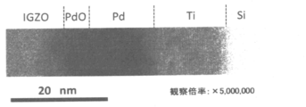
- FIG. 4 is a cross-sectional TEM image of a laminated electrode produced in Example 2.
- FIG. 6 is a cross-sectional view schematically showing elements produced in Examples 16 to 28.
- One embodiment of the laminate of the present invention includes a substrate, one or more layers selected from a contact resistance reduction layer and a reduction suppression layer, a Schottky electrode layer, and a metal oxide semiconductor layer in this order.
- the Schottky barrier diode can be formed regardless of the substrate and the base material.
- One or more layers selected from the contact resistance reduction layer and the reduction suppression layer are preferably in contact with the Schottky electrode layer, and the Schottky electrode layer and the metal oxide semiconductor layer are preferably in contact.
- Another embodiment of the laminate of the present invention has at least a Schottky electrode layer and a metal oxide semiconductor layer in this order on a conductive substrate, and reduces contact resistance between the conductive substrate and the Schottky electrode layer. It has one or more layers selected from a layer and a reduction suppression layer.
- the one embodiment of the laminate of the present invention and the other embodiment of the laminate of the invention are collectively referred to as the laminate of the present invention.
- the contact resistance reducing layer and the reduction suppressing layer may include both or only one of them.
- the laminated body of this invention may laminate
- the laminate according to the present invention has the above-described configuration, so that the on-resistance in the forward direction can be reduced when used in a semiconductor element. Further, the reverse leakage current can be reduced, the power loss can be reduced, and the current can be extracted.
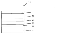
- Examples of the layer structure of the laminate of the present invention include the following structures. (1) substrate // contact resistance reduction layer / Schottky electrode layer / metal oxide semiconductor layer (2) substrate // reduction suppression layer / Schottky electrode layer / metal oxide semiconductor layer (3) substrate // contact resistance reduction Layer / reduction suppression layer / Schottky electrode layer / metal oxide semiconductor layer (“/” indicates that each layer is laminated adjacently) ("//" indicates that the layers are stacked without being adjacent to each other.)
- the following structure can be mentioned as a layer structure which laminated
- substrate // contact resistance reduction layer / Schottky electrode layer / metal oxide semiconductor layer / ohmic electrode layer (5) substrate // reduction suppression layer / Schottky electrode layer / metal oxide semiconductor layer / ohmic electrode layer ( 6)
- Substrate // Contact resistance reduction layer / Reduction suppression layer / Schottky electrode layer / Metal oxide semiconductor layer / Ohmic electrode layer
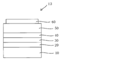
- the laminated structure (6) above is shown in FIG.
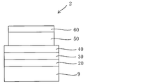
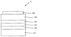
- the contact resistance reducing layer 20, the reduction suppressing layer 30, the Schottky electrode layer 40, the metal oxide semiconductor layer 50, and the ohmic electrode layer 60 are stacked in this order on the substrate 9.
- the outer edge (end part) of the metal oxide semiconductor layer 50 may be the same as the outer edge (end part) of the Schottky electrode layer 40 or may be located inside the outer edge of the Schottky electrode layer 40. Good. The latter case is shown as a laminate 2 in FIG.
- symbol shall mean the same structure.
- the outer edge (end portion) of the ohmic electrode layer 60 may be the same as the outer edge (end portion) of the metal oxide semiconductor layer 50 or may be positioned inside the outer edge of the metal oxide semiconductor layer 50. May be. The latter case is shown as a laminate 3 in FIG. Each configuration will be described later.
- conductive substrate / contact resistance reduction layer / Schottky electrode layer / metal oxide semiconductor layer (12) conductive substrate / reduction suppression layer / Schottky electrode layer / metal oxide semiconductor layer (13) conductive substrate / Contact resistance reduction layer / reduction suppression layer / Schottky electrode layer / metal oxide semiconductor layer (“/” indicates that each layer is laminated adjacently)
- the following structure can also be mentioned as a layer structure which laminated
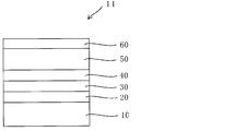
- Conductive substrate / contact resistance reduction layer / Schottky electrode layer / metal oxide semiconductor layer / ohmic electrode layer (15) Conductive substrate / reduction suppression layer / Schottky electrode layer / metal oxide semiconductor layer / ohmic electrode Layer (16) conductive substrate / contact resistance reduction layer / reduction suppression layer / Schottky electrode layer / metal oxide semiconductor layer / ohmic electrode layer
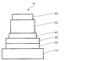
- FIG. 4 shows the layered structure (16) above.
- the contact resistance reducing layer 20, the reduction suppressing layer 30, the Schottky electrode layer 40, the metal oxide semiconductor layer 50, and the ohmic electrode layer 60 are stacked in this order on the conductive substrate 10.
- the outer edge (end part) of the metal oxide semiconductor layer 50 may be the same as the outer edge (end part) of the Schottky electrode layer 40 or may be located inside the outer edge of the Schottky electrode layer 40. Good. The latter case is shown as a laminate 12 in FIG. In this case, the Schottky electrode layer 40 covers the lower surface of the metal oxide semiconductor layer 50, that is, the entire lower surface of the metal oxide semiconductor layer 50 is in contact with the Schottky electrode layer 40.
- the end of the semiconductor is not in direct contact with the Schottky electrode in order to achieve a high withstand voltage.
- the metal oxide semiconductor since the metal oxide semiconductor has little leakage current at the film end, the end of the metal oxide semiconductor layer can be the same as or inside the end of the Schottky metal layer. Become. By doing so, it is possible to prevent the electric field from concentrating on the end portion of the semiconductor layer when a reverse bias is applied, and to realize a high withstand voltage.
- the outer edge (end portion) of the ohmic electrode layer 60 may be the same as the outer edge (end portion) of the metal oxide semiconductor layer 50 or may be positioned inside the outer edge of the metal oxide semiconductor layer 50. May be. The latter case is shown as a laminate 13 in FIG. In this case, the metal oxide semiconductor layer 50 is configured to cover the lower surface of the ohmic electrode layer 60.
- FIGS. 2 and 3 can be applied to a stacked configuration other than the stacked configuration of Formula (6). Moreover, the structure shown in FIG. 2 and FIG. 3 can also be provided simultaneously. 5 and FIG. 6 can also be applied to a stacked configuration other than the stacked configuration of Expression (16). Moreover, the structure shown in FIG. 5 and FIG. 6 can also be provided simultaneously.
- FIG. 7 shows another embodiment of the laminated structure (16).
- the laminated body 14 in FIG. 7 has a laminated structure in which the structures shown in FIGS. 5 and 6 are provided at the same time, and the outer edge (end part) of the Schottky electrode layer 40 is the outer edge (end part) of the reduction suppressing layer 30.
- the outer edge (end part) of the contact resistance reducing layer 20 is located inside the outer edge (end part) of the conductive substrate 10.
- the substrate is not particularly limited and a known material can be used, and examples thereof include a conductive substrate, a semiconductor substrate, and an insulating substrate.
- the conductive substrate examples include a silicon substrate and a metal substrate.
- a low-resistance silicon substrate having a high impurity doping concentration is preferable, and an n-type low-resistance silicon substrate is more preferable.
- Conventionally known B, P, Pb, As, etc. can be used as the dopant.
- the silicon substrate preferably has a low resistance.
- the volume resistivity ⁇ of the silicon substrate is preferably 100 m ⁇ cm or less, more preferably 10 m ⁇ cm or less, and further preferably 5 m ⁇ cm or less.
- the metal of the metal substrate examples include Cu, Al, Au, Cr, Fe, Ni, and W. These alloys can also be used. Preferably, Cu, Al, or an alloy thereof is low resistance, low cost, and excellent thermal conductivity. When a metal substrate is used as the conductive substrate, this metal substrate can also serve as a contact resistance reducing layer.
- the laminate of the present invention can provide a Schottky barrier diode that exhibits good diode characteristics even when an inexpensive silicon substrate or metal substrate is used as a conductive substrate.
- the thickness of the conductive substrate is usually 200 ⁇ m to 2 mm.
- the material of the semiconductor substrate is not particularly limited as long as the surface smoothness is maintained.
- a semiconductor substrate a Si substrate, a GaN substrate, a SiC substrate, a GaP substrate, a GaAs substrate, a ZnO substrate, a Ga 2 O 3 substrate, a GaSb substrate, an InP substrate, and an InAs whose carrier concentration is adjusted to 1 ⁇ 10 18 cm ⁇ 3 or less.
- Examples include a substrate, an InSb substrate, a ZnS substrate, a ZnTe substrate, and a diamond substrate.
- the semiconductor substrate may be single crystal or polycrystalline. Further, an amorphous substrate or a substrate partially containing amorphous may be used.
- a substrate in which a semiconductor film is formed using a technique such as CVD (chemical vapor deposition) on a conductor substrate, a semiconductor substrate, or an insulating substrate may be used.
- the thickness of the semiconductor substrate is usually 200 ⁇ m to 2 mm.
- the thickness is preferably 200 ⁇ m to 1 mm, more preferably 200 ⁇ m to 700 ⁇ m.
- the insulating substrate is not particularly limited as long as it is an insulating substrate, and a substrate generally used can be arbitrarily selected as long as the effects of the present invention are not lost.
- a substrate generally used can be arbitrarily selected as long as the effects of the present invention are not lost.
- the insulating substrate for example, quartz glass, barium borosilicate glass, aluminoborosilicate glass, aluminosilicate glass, etc., alkali-free glass substrate produced by the fusion method or float method, ceramic substrate, and processing temperature of this production process And a plastic substrate having heat resistance that can withstand heat.
- a dielectric substrate may also be used as the insulating substrate.
- the dielectric substrate include a lithium niobate substrate, a lithium tantalate substrate, a zinc oxide substrate, a quartz substrate, and a sapphire substrate.
- an insulating substrate or a dielectric substrate in which an insulating film or a dielectric film is provided on the surface of a metal substrate such as a stainless alloy may be used.
- an insulating film may be formed over the substrate as a base film.
- a single layer or a stacked layer such as a silicon oxide film, a silicon nitride film, a silicon oxynitride film, or a silicon nitride oxide film can be formed by a CVD method, a sputtering method, or the like.
- the thickness of the insulating substrate is not particularly limited, but is 2 ⁇ m to 2 mm, for example.
- the thickness is preferably 2 ⁇ m to 1 mm, more preferably 2 ⁇ m to 700 ⁇ m.
- a base material having an arbitrary structure, layer structure, circuit, wiring, electrode, or the like made of a plurality of materials may be used on the above-described conductive substrate, semiconductor substrate, or insulating substrate.
- Examples of materials having an arbitrary structure include composite materials of various metals and insulators such as a metal that forms a back end of line on a large scale integrated circuit (LSI), an interlayer insulating film, and the like.
- LSI large scale integrated circuit
- interlayer insulating film and the like.
- substrate is not specifically limited, Preferably it is 150 nm or less, More preferably, it is 50 nm or less, More preferably, it is 10 nm or less.
- the smoothness of the Schottky electrode layer is maintained when the contact resistance reduction layer, the reduction suppression layer, and the Schottky electrode layer are stacked, and the device is evaluated as an element. The leakage current in the reverse direction is kept low.
- the surface roughness of the substrate can be determined, for example, by the method described in the examples.
- the layer structure is not particularly limited, and is an electrode layer, an insulating layer, a semiconductor layer, a dielectric layer, a protective film layer, a stress buffer layer, a light shielding layer, an electron / hole injection layer, an electron / hole transport layer, a light emitting layer.
- Known layers such as an electron / hole blocking layer, a crystal growth layer, an adhesion improving layer, a memory layer, a liquid crystal layer, a capacitor layer, and a power storage layer can be used.
- an insulating layer generally Al, Si, Sc, Ti, V, Cr, Ni, Cu, Zn, Ga, Ge, Y, Zr, Nb, Mo, Tc, Ru, Rh, Pd, Ag, Cd, In, Examples thereof include an oxide insulating film and a nitride film containing one or more metals selected from the group consisting of Sn, Sb, Te, Hf, Ta, W, Re, Os, Ir, Pt, and Au.
- oxide semiconductor layers, organic semiconductor layers such as pentacene, and the like are widely used regardless of the crystalline state of single crystal, polycrystal, or amorphous.
- a lithium niobate layer As the dielectric layer, a lithium niobate layer, a lithium tantalate layer, a zinc oxide layer, a quartz substrate layer, a sapphire layer, a BaTiO 3 layer, a Pb (Zr, Ti) O 3 (PZT) layer, (Pb, La) ( Zr, Ti) O 3 (PLZT) layer, Pb (Zr, Ti, Nb) O 3 (PZTN) layer, Pb (Ni, Nb) O 3 —PbTiO 3 (PNN-PT) layer, Pb (Ni, Nb) O 3 —PbZnO 3 (PNN—PZ) layer, Pb (Mg, Nb) O 3 —PbTiO 3 (PMN—PT) layer, SrBi 2 Ta 2 O 9 (SBT) layer, (K, Na) TaO 3 layer, (K, Na) NbO 3 layer, BiFeO 3 layer, Bi (Nd, La
- the protective film layer As a film of the protective film layer, a film having excellent insulating properties regardless of inorganic materials and organic materials and low permeability of water or the like can be used.
- Examples of the stress buffer layer include an AlGaN layer.
- Examples of the light shielding layer include a black matrix layer containing a metal, a metal-organic material, and a color filter layer.
- Examples of the electron / hole injection layer include an oxide semiconductor layer and an organic semiconductor layer.
- Examples of the electron / hole transport layer include an oxide semiconductor layer and an organic semiconductor layer.
- Examples of the light emitting layer include an inorganic semiconductor layer and an organic semiconductor layer.
- Examples of the electron / hole blocking layer include an oxide semiconductor layer.
- Examples of the base material include a power generation device, a light emitting device, a sensor, a power conversion device, an arithmetic device, a protection device, an optoelectronic device, a display, a memory, a semiconductor device having a back end of line, and a power storage device.
- the layer having a layer structure may be a single layer or two or more layers.
- the contact resistance reducing layer plays a role of preventing the interaction between the base substrate and the Schottky electrode metal. In addition, it improves the adhesion of the Schottky electrode to the underlying substrate and improves the surface smoothness of the Schottky electrode. That is, it is a layer for reducing the contact resistance when the substrate and the Schottky electrode are directly laminated.
- the substrate and the Schottky electrode are directly laminated, for example, when an n-type low-resistance silicon substrate is used as the substrate and these are directly laminated using palladium oxide for the Schottky electrode, the palladium oxide and Si are in the opposite directions. A -n junction is formed and becomes a large resistance component in the forward direction. Further, the interface between Si and palladium oxide is not smooth, and as a result, the smoothness of the surface of the Schottky electrode is lost, and there is a possibility that the withstand voltage is lowered.
- one or more metals selected from Ti, Mo, Ag, In, Al, W, Co, and Ni, alloys thereof, or silicides thereof can be used.
- Ti, Mo, Ag, In, or Al that forms a low-resistance silicide and more preferably Ti or Mo that forms a good Schottky contact when combined with a low-resistance and Schottky metal.
- Mo has a high thermal conductivity. Since Mo is excellent in heat dissipation and has high thermal conductivity, element degradation is less likely to occur due to Joule heat due to current when the diode is driven.
- the thickness of the contact resistance reducing layer is usually 1 nm to 1 ⁇ m, preferably 2 nm to 500 nm, more preferably 5 nm to 500 nm. If it is this range, it has sufficient adhesiveness and there is little increase in resistance. More preferably, it is 10 nm to 500 nm.
- the in-plane coverage of the contact resistance reducing layer is high, and it is easy to obtain characteristics with small in-plane resistance variation in the forward direction when the diode is driven. Furthermore, when used as an element for taking out a current in the lateral direction, the wiring resistance is lowered and a high current value is easily obtained.
- the contact resistance reduction layer can be confirmed by cross-sectional TEM observation or secondary ion mass spectrometry. The same applies to the ohmic electrode, the metal oxide semiconductor layer, the reduction suppressing layer, the Schottky electrode layer, and the substrate.
- the reduction suppression layer is a layer that prevents reduction of the Schottky electrode layer. If the reduction suppressing layer is provided, the reduction of the Schottky electrode layer is suppressed, and the Schottky interface is formed without any problem.
- metal used for the reduction suppression layer one or more kinds selected from Pd, Mo, Pt, Ir, Ru, Au, Ni, W, Cr, Re, Te, Tc, Mn, Os, Fe, Rh, and Co. Element and these alloys are mentioned.
- the reduction suppressing layer that is, the metal oxide metal constituting the Schottky electrode layer.
- the combination of the reduction suppressing layer and the Schottky electrode layer include Pd / palladium oxide, Pt / platinum oxide, Ir / iridium oxide, Ru / ruthenium oxide, and the like.
- the thickness of the reduction suppressing layer is usually 1 nm to 1 ⁇ m, preferably 2 nm to 500 nm, more preferably 5 nm to 100 nm, and particularly preferably 10 nm to 50 nm. Within this range, since the reduction suppressing effect is excellent, the on-resistance during forward bias can be reduced. In addition, the flatness of the Schottky interface can be improved.
- the work function of the metal contained in the Schottky electrode layer is preferably 3.7 eV or more, more preferably 4.4 eV or more, and further preferably 4.7 eV or more.
- the upper limit of the work function is not particularly specified, but is usually 6.5 eV.
- Pd oxide, Pt oxide, Ir oxide or Ru oxide is preferable.
- a high Schottky barrier can be formed by a combination with a metal oxide semiconductor.
- the carrier concentration of the Schottky electrode layer is preferably 1 ⁇ 10 18 cm ⁇ 3 or more.
- the carrier concentration can be obtained, for example, by hole measurement.
- the thickness of the Schottky electrode layer is usually 1 nm to 1 ⁇ m, preferably 2 nm to 100 nm, more preferably 5 nm to 50 nm. Within this range, the on-resistance during forward bias is excellent. In addition, the flatness of the Schottky interface can be improved and the voltage resistance is excellent.
- the production method for obtaining the metal oxide of the Schottky electrode is not particularly limited, and examples thereof include a method of performing reactive sputtering of a metal target in an oxygen-containing atmosphere.
- the composition of the metal oxide semiconductor layer is not particularly limited as long as it is a metal oxide semiconductor.
- An oxide containing one or more elements selected from In, Ga, Zn, and Sn is preferable. Examples thereof include an oxide semiconductor (IGZO) of In, Ga, and Zn.
- IGZO oxide semiconductor
- Hydrogen concentration of the metal oxide semiconductor layer is preferably from 10 17 to 10 22 / cm 3, more preferable to be 10 19 to 10 22 / cm 3, more preferably 10 20 to 10 21 / cm 3.
- Oxide semiconductors easily form oxygen vacancies, and leakage current may flow through the vacancies. However, oxygen vacancies are terminated with hydroxyl groups by increasing the hydrogen atom concentration in the film to 10 20 atoms / cm 3 or more. Leakage current can be reduced.
- the hydrogen atom concentration is measured by secondary ion mass spectrometry.
- the method for adjusting the hydrogen atom concentration is not particularly limited, but can be adjusted by optimizing the atmosphere during film formation, annealing after film formation, and the atmosphere during film formation of the ohmic electrode.
- the free carrier concentration of the metal oxide semiconductor layer is usually 1 ⁇ 10 13 cm ⁇ 3 or more and less than 1 ⁇ 10 18 cm ⁇ 3 .
- the free carrier concentration can be obtained, for example, by hole measurement.
- the band gap of the metal oxide semiconductor layer is preferably 2.0 eV to 6.0 eV, more preferably 2.5 eV to 5.5 eV, and further preferably 3.0 eV to 5.0 eV.
- the band gap is measured by the method described in the examples.
- the thickness of the metal oxide semiconductor layer is usually 10 nm to 10 ⁇ m, preferably 50 nm to 7 ⁇ m, more preferably 100 nm to 5 ⁇ m.
- the film thickness can be selected so as to obtain a desired withstand voltage. If it is too thick, the resistance during forward bias may increase.
- the laminate of the present invention can provide a Schottky barrier diode that exhibits good diode characteristics even when a metal oxide semiconductor layer is formed by a method having excellent productivity such as sputtering.
- the material of the ohmic electrode layer is not particularly limited as long as a good ohmic connection with the metal oxide semiconductor layer can be achieved, but one or more elements selected from the group consisting of Mo, Ti, Au, Ag, and Al and alloys thereof Is mentioned.
- the ohmic electrode layer can be composed of a plurality of layers.
- a Mo electrode layer can be used on the side in contact with the metal oxide semiconductor layer, and a metal layer of Au or Al can be stacked. In this way, power loss can be reduced and current can be extracted.
- the thickness of the ohmic electrode layer is not particularly limited, but is usually 100 nm to 5 ⁇ m.
- the film forming method of each layer is not particularly limited, but the CVD method such as thermal CVD method, CAT-CVD method, photo CVD method, mist CVD method, MO-CVD method, plasma CVD method, atomic level control such as MBE, ALD, etc.
- CVD method such as thermal CVD method, CAT-CVD method, photo CVD method, mist CVD method, MO-CVD method, plasma CVD method, atomic level control such as MBE, ALD, etc.
- Conventionally known ceramic processes such as PVD methods such as film forming method, ion plating, ion beam sputtering, magnetron sputtering, doctor blade method, injection method, extrusion method, hot press method, sol-gel method, aerosol deposition method are used.
- a wet method such as a method, a coating method, a spin coating method, a printing method, a spray method, an electrodeposition method, a plating method, or a micellar electrolysis method can be used.
- the laminated body of the present invention includes a power semiconductor element, a (rectifier) diode element, a Schottky barrier diode element, an electrostatic discharge (ESD) protection diode, a transient voltage protection (TVS) protection diode, a light emitting diode, and a metal semiconductor field effect transistor (MESFET). ), Junction field effect transistor (JFET), metal oxide semiconductor field effect transistor (MOSFET), Schottky source / drain MOSFET, avalanche multiplication type photoelectric conversion element, solid-state imaging device, solar cell element, photosensor element, display It can be used for semiconductor elements such as elements and resistance change memories.
- the semiconductor element can be used for a Schottky barrier diode or a junction transistor.
- An electronic circuit using this element, a Schottky barrier diode, or a junction transistor can be used in an electric device, an electronic device, a vehicle, a power engine, and the like.
- Example 1 [Production of Schottky barrier diode] A Schottky barrier diode element was fabricated as follows. An n-type Si substrate (diameter 4 inches) having a resistivity of 1 m ⁇ ⁇ cm was mounted on a sputtering apparatus (manufactured by Anelva: E-200S), and Ti was deposited to a thickness of 15 nm as a contact resistance reducing layer. The film forming conditions were a DC 50 W, Ar atmosphere. Next, 10 nm of palladium oxide was deposited as a Schottky electrode layer (carrier concentration: 1 ⁇ 10 20 cm ⁇ 3 ). Film forming conditions, DC50W, and a mixed gas atmosphere of Ar and O 2.
- this substrate was set in a sputtering apparatus (ULVAC: CS-200) together with Area Max, and 200 nm of IGZO having the composition shown in Table 1 was formed as a metal oxide semiconductor layer (free carrier concentration: 5 ⁇ 10 16 cm ⁇ 3 ).
- the film forming conditions were DC 300 W and a gas flow rate ratio shown in Table 1.
- the substrate was taken out and annealed in an electric furnace at 300 ° C. for 1 hour in air.
- This substrate was set again in a sputtering apparatus together with Area Max, and then Mo was deposited to a thickness of 150 nm as an ohmic electrode layer.
- the film forming conditions were DC 100 W, Ar atmosphere.
- the free carrier concentration of the metal oxide semiconductor layer and the carrier concentration of the Schottky electrode layer were measured as follows. It performed through the metal oxide semiconductor layer film-forming process (or Schottky electrode layer film-forming process) with respect to the glass substrate. Then, each substrate was cut into 1 cm square, and In electrodes were provided at the four corners to obtain Hall effect measurement elements.
- the free carrier concentration (carrier concentration) is measured at room temperature using a Hall effect measuring device (manufactured by ACCENT: HL-5500PC), and the resulting free carrier amount (carrier amount) is measured on the metal semiconductor layer.
- the free carrier concentration (carrier concentration) was normalized by the volume (or the Schottky electrode volume).
- the band gap of the metal oxide semiconductor layer was evaluated as follows. The process up to the step of forming the metal oxide semiconductor layer in the above Schottky barrier diode manufacturing process was performed on the substrate, and the obtained laminate was cut into 1 cm square. Using a spectroscopic ellipsometry measuring device (manufactured by JA Woollam Japan Co., Ltd .: M-2000D) at room temperature, the incident angle of polarized light is changed to 50 °, 60 °, 70 ° from the direction perpendicular to the substrate, The measurement was performed at a measurement wavelength of 192.3 nm to 1689 nm and a measurement width of 3.4 nm.
- the absorption coefficient ⁇ was calculated.
- the spectrum of the absorption coefficient alpha of the metal oxide semiconductor layer, by plotting the alpha 2 relative to the energy range 2 eV ⁇ 5 eV of light was calculated intersection of the energy axis which is extended linearly as a band gap. The results are shown in Table 1.
- the hydrogen atom concentration of the metal oxide semiconductor layer was evaluated as follows. The measurement was carried out by a quadrupole secondary ion mass spectrometer (manufactured by ULVAC-PHI, Inc .: D-SIMS) under measurement conditions of a Cs ion source of 1 kV, a primary ion current of 100 nA, and a chamber vacuum degree of 5 ⁇ 10 ⁇ 10 torr.
- the hydrogen atom concentration of the metal oxide semiconductor layer is determined based on the hydrogen secondary ion intensity obtained by the quadrupole secondary ion mass spectrometer integrated with the thickness of the metal semiconductor thin film.
- the strength was normalized by using an In—Ga—Zn—O thin film with a known concentration and film thickness, and the hydrogen concentration was quantified. The obtained value was defined as the hydrogen atom concentration.
- Table 1 The results are shown in Table 1.
- Example 2 A device was fabricated in the same manner as in Example 1 except that 20 nm of Pd was deposited as a reduction suppressing layer following the formation of the contact resistance reducing layer.
- the film forming conditions were a DC 50 W, Ar atmosphere.
- a cross-sectional TEM image obtained by an electron microscope (manufactured by JEOL: JEM-2800) of the laminated electrode is shown in FIG.
- the obtained element Si / Ti / Pd / palladium oxide / IGZO / Mo
- the obtained element was evaluated in the same manner as in Example 1. The results are shown in Table 1.
- the obtained element has a structure shown in FIG.
- Example 3 Following the formation of the contact resistance reducing layer, a device was fabricated in the same manner as in Example 1 except that Ru was deposited to a thickness of 20 nm as a reduction suppressing layer and then ruthenium oxide was deposited to a thickness of 10 nm as a Schottky electrode.
- the Ru film formation conditions were DC 50 W, Ar atmosphere, and the ruthenium oxide film formation conditions were DC 50 W, a mixed gas atmosphere of Ar and O 2 (carrier concentration: 1 ⁇ 10 20 cm ⁇ 3 ).
- the obtained element Si / Ti / Ru / ruthenium oxide / IGZO / Mo
- the obtained element was evaluated in the same manner as in Example 1. The results are shown in Table 1.
- the obtained element has a structure shown in FIG.
- Example 4 Following the formation of the contact resistance reducing layer, a device was fabricated in the same manner as in Example 1 except that 20 nm of Pt was formed as a reduction suppressing layer and then 10 nm of platinum oxide was formed as a Schottky electrode.
- the Pt film formation conditions were DC 50 W and Ar atmosphere, and the platinum oxide film formation conditions were DC 50 W and a mixed gas atmosphere of Ar and O 2 (carrier concentration: 1 ⁇ 10 20 cm ⁇ 3 ).
- the obtained element Si / Ti / Pt / platinum oxide / IGZO / Mo
- the obtained element was evaluated in the same manner as in Example 1. The results are shown in Table 1.
- the obtained element has a structure shown in FIG.
- Example 5 Following the formation of the contact resistance reducing layer, an element was fabricated in the same manner as in Example 1 except that Ir was deposited to a thickness of 20 nm as a reduction suppression layer, and then iridium oxide was deposited to a thickness of 10 nm as a Schottky electrode.
- the Ir film formation conditions were DC 50 W and Ar atmosphere, and the iridium oxide film formation conditions were DC 50 W and a mixed gas atmosphere of Ar and O 2 (carrier concentration: 1 ⁇ 10 20 cm ⁇ 3 ).
- the obtained element Si / Ti / Ir / iridium oxide / IGZO / Mo
- the obtained element was evaluated in the same manner as in Example 1. The results are shown in Table 1.
- the obtained element has a structure shown in FIG.
- the devices obtained in Examples 2 to 5 exhibited good diode characteristics with an on-resistance Ron of less than 1 m ⁇ cm 2 and a leakage current Ir of 3 ⁇ 10 ⁇ 8 A / cm
- Comparative Example 1 A device was fabricated in the same manner as in Example 1 except that the contact resistance reducing layer was not formed.
- the obtained element Si / palladium oxide / IGZO / Mo
- the results are shown in Table 1.
- the device obtained in Comparative Example 1 had a high on-resistance Ron of 200 m ⁇ cm 2 or more, and the leakage current Ir was 2 ⁇ 10 ⁇ 3 A / cm 2 .
- Examples 6-9 A device was fabricated in the same manner as in Example 2 except that the reduction suppressing layer and the Schottky electrode layer were changed to the combinations shown in Table 2 with respect to Example 2. The obtained device was evaluated in the same manner as in Example 1. The results are shown in Table 2. The devices obtained in Examples 6 to 9 exhibited good diode characteristics with an on-resistance Ron of less than 10 m ⁇ cm 2 and a leakage current Ir of 5 ⁇ 10 ⁇ 8 A / cm 2 or less.
- Examples 10-12 A device was fabricated in the same manner as in Example 2 except that the thickness of the Schottky electrode layer was changed as described in Table 3 with respect to Example 2. The obtained device was evaluated in the same manner as in Example 1. The results are shown in Table 3.
- the devices obtained in Examples 10 and 11 had good diode characteristics with an on-resistance Ron of less than 1 m ⁇ cm 2 and a leakage current Ir of 1 ⁇ 10 ⁇ 7 A / cm 2 or less.
- the device obtained in Example 12 had an on-resistance Ron of less than 10 m ⁇ cm 2 and a leakage current Ir of 3 ⁇ 10 ⁇ 5 A / cm 2 or less.
- Examples 13-15 A device was fabricated in the same manner as in Example 2 except that the Schottky electrode layer and the reduction suppression layer were changed as described in Table 4 with respect to Example 2. The obtained device was evaluated in the same manner as in Example 1. The results are shown in Table 4.
- the device obtained in Example 13 had good diode characteristics with an on-resistance Ron of less than 1 m ⁇ cm 2 and a leakage current Ir of 5 ⁇ 10 ⁇ 7 A / cm 2 or less.
- the devices obtained in Examples 14 and 15 had a low on-resistance Ron of less than 1 m ⁇ cm 2 , and the leakage currents Ir were 2 ⁇ 10 ⁇ 3 A / cm 2 and 7 ⁇ 10 ⁇ 1 A / cm 2 , respectively. there were.
- Examples 16-19 An element was manufactured on a substrate shown in Table 5 using a photomask.
- the film forming conditions of Example 2 and each layer are the same.
- FIG. 9 shows the structure of the obtained element (laminated body) 15.
- Ti was sputtered on the one surface of the substrate 8 as the contact resistance reducing layer 20, and Pd was sputtered as the reduction suppressing layer 30 at 15 nm and 20 nm, respectively.
- the Ti / Pd laminated film was patterned using a photomask.
- AZ1500 manufactured by AZ Electronic Materials
- TMAH tetramethylammonium hydroxide
- AURUM-302 manufactured by Kanto Chemical
- AZ5214 manufactured by AZ Electronic Materials
- AZ5214 was exposed through a photomask, exposed on the entire surface after the reverse baking step, and developed with tetramethylammonium hydroxide (TMAH).
- TMAH tetramethylammonium hydroxide
- the interlayer insulating film 70 was patterned using a thermosetting non-photosensitive polyimide and a photomask. Specifically, first, a thermosetting non-photosensitive polyimide solution was applied on the entire surface of the substrate with a spin coater, and then patterned using AZ5214 and a photomask. AZ5214 was exposed through a photomask, exposed on the entire surface after the reverse baking step, and developed with tetramethylammonium hydroxide (TMAH). Subsequently, the thermosetting non-photosensitive polyimide was etched with TMAH and patterned. After patterning, the thermosetting non-photosensitive polyimide was heated and cured in the atmosphere at 200 ° C. for 1 hour.
- TMAH tetramethylammonium hydroxide
- the ohmic electrode layer 60 was patterned by a lift-off process using an image reversal resist AZ5214 and a photomask.
- AZ5214 was exposed through a photomask, exposed on the entire surface after the reverse baking step, and developed with tetramethylammonium hydroxide (TMAH).
- TMAH tetramethylammonium hydroxide
- Mo 150 nm was deposited as an ohmic electrode layer, and then an Au layer 80 was deposited to 500 nm. Thereafter, the ohmic electrode layer 60 was patterned by lifting off in acetone.
- the element was measured by grounding the probe on the ohmic electrode side and connecting it to the ground, grounding the probe in a region where the ohmic electrode and Au were directly laminated on the reduction suppression layer, and changing the voltage. Other evaluations were performed in the same manner as in Example 1. The results are shown in Table 5.
- the carrier concentration of the Schottky electrode layer was 1 ⁇ 10 20 cm ⁇ 3 .
- the devices obtained in Examples 16 to 18 had good diode characteristics with an on-resistance Ron of less than 1 m ⁇ cm 2 and a leakage current Ir of 5 ⁇ 10 ⁇ 8 A / cm 2 or less.
- the device obtained in Example 19 had a leakage current Ir of 1 ⁇ 10 ⁇ 1 A / cm, which was higher than those in Examples 16 to 18.
- the surface roughness of the substrate was measured by observing the fabricated device with a cross-sectional TEM (transmission electron microscope) image and EDX (energy dispersive X-ray spectroscopy). The specific procedure is shown below.
- the area where the constituent elements of each substrate shown in Table 5 were detected by EDX was defined as the substrate, and the interface was defined from the difference in contrast between the substrate and the ohmic electrode layer in the cross-sectional TEM image.
- the arithmetic average roughness Ra was calculated from the equation (1) with respect to the unevenness of the substrate interface to obtain surface roughness. The results are shown in Table 5.
- the crystallinity of the substrate was evaluated by an electron diffraction image obtained by an electron microscope (manufactured by JEOL: JEM-2800). In the electron beam irradiation area, a diffraction image was obtained from a region having a diameter of 10 nm or more with respect to the cross section of the substrate. Those in which the spot shape was observed in the diffraction image were judged as single crystals, and those in the ring shape were judged as polycrystalline. The results are shown in Table 5.
- Examples 20-23 A device was fabricated in the same manner as in Example 16 except that the insulating substrate shown in Table 6 was used. The obtained device was evaluated in the same manner as in Example 16. The results are shown in Table 6. The carrier concentration of the Schottky electrode layer was 1 ⁇ 10 20 cm ⁇ 3 . The devices obtained in Examples 20 to 23 exhibited good diode characteristics with an on-resistance Ron of less than 1 m ⁇ cm 2 and a leakage current Ir of 3 ⁇ 10 ⁇ 7 A / cm 2 or less.
- Examples 24-28 A device was fabricated in the same manner as in Example 2 except that the metal oxide semiconductor layer was formed with the metal composition shown in Table 7 and the ratio of the introduced gas during film formation. The obtained device was evaluated in the same manner as in Example 1. The results are shown in Table 7. The obtained element has a structure shown in FIG. The devices obtained in Examples 24 to 28 exhibited good diode characteristics with an on-resistance Ron of less than 1 m ⁇ cm 2 and a leakage current Ir of 2 ⁇ 10 ⁇ 6 A / cm 2 or less.
- Examples 29-33 A device was fabricated in the same manner as in Example 2 except that the metal oxide semiconductor layer was formed with the metal composition shown in Table 8 and the ratio of the introduced gas during film formation. The obtained device was evaluated in the same manner as in Example 1. The results are shown in Table 8. As a result of evaluating the hydrogen atom concentration of the devices obtained in Examples 29 to 31, they were 8 ⁇ 10 20 cm ⁇ 3 , 5 ⁇ 10 21 cm ⁇ 3 , and 5 ⁇ 10 20 cm, respectively. The devices obtained in Examples 29 to 31 exhibited good diode characteristics with an on-resistance Ron of less than 1 m ⁇ cm 2 and a leakage current Ir of 2 ⁇ 10 ⁇ 8 A / cm 2 or less.
- the hydrogen atom concentration of the devices obtained in Examples 32 and 33 were 4 ⁇ 10 15 cm ⁇ 3 and 8 ⁇ 10 16 cm ⁇ 3 , respectively.
- the devices obtained in Examples 32 and 33 had an on-resistance Ron of less than 1 m ⁇ cm 2 , but the leakage currents Ir were 9 ⁇ 10 ⁇ 1 A / cm 2 and 1 ⁇ 10 ⁇ 2 A / cm 2 , respectively. there were.
- Examples 34-35 A device was fabricated in the same manner as in Example 2 except that the contact resistance reducing layer or the ohmic electrode layer was changed to the material shown in Table 9. The obtained device was evaluated in the same manner as in Example 1. The results are shown in Table 9. The devices obtained in Examples 34 and 35 had an on-resistance Ron of less than 1 m ⁇ cm 2 , but the leakage currents Ir were 1 ⁇ 10 ⁇ 1 A / cm 2 and 3 ⁇ 10 ⁇ 8 A / cm 2 , respectively. There was good diode characteristics.
- the laminate of the present invention can be used for a semiconductor element such as a power semiconductor element, a diode element, and a Schottky barrier diode element, and an electronic circuit using the element is used for an electric device, an electronic device, an electric vehicle, and the like. Can do.
- a semiconductor element such as a power semiconductor element, a diode element, and a Schottky barrier diode element
Landscapes
- Engineering & Computer Science (AREA)
- Microelectronics & Electronic Packaging (AREA)
- Power Engineering (AREA)
- General Physics & Mathematics (AREA)
- Computer Hardware Design (AREA)
- Physics & Mathematics (AREA)
- Condensed Matter Physics & Semiconductors (AREA)
- Ceramic Engineering (AREA)
- Manufacturing & Machinery (AREA)
- Chemical & Material Sciences (AREA)
- Crystallography & Structural Chemistry (AREA)
- Electrodes Of Semiconductors (AREA)
- Laminated Bodies (AREA)
Priority Applications (4)
| Application Number | Priority Date | Filing Date | Title |
|---|---|---|---|
| JP2017558338A JP6976858B2 (ja) | 2015-12-25 | 2016-12-26 | 積層体 |
| CN201680075286.7A CN108475702B (zh) | 2015-12-25 | 2016-12-26 | 层叠体 |
| KR1020187016344A KR102382656B1 (ko) | 2015-12-25 | 2016-12-26 | 적층체 |
| US16/065,239 US11189737B2 (en) | 2015-12-25 | 2016-12-26 | Laminated body |
Applications Claiming Priority (4)
| Application Number | Priority Date | Filing Date | Title |
|---|---|---|---|
| JP2015254555 | 2015-12-25 | ||
| JP2015-254555 | 2015-12-25 | ||
| JP2016159352 | 2016-08-15 | ||
| JP2016-159352 | 2016-08-15 |
Publications (1)
| Publication Number | Publication Date |
|---|---|
| WO2017111174A1 true WO2017111174A1 (ja) | 2017-06-29 |
Family
ID=59090563
Family Applications (1)
| Application Number | Title | Priority Date | Filing Date |
|---|---|---|---|
| PCT/JP2016/088765 WO2017111174A1 (ja) | 2015-12-25 | 2016-12-26 | 積層体 |
Country Status (6)
| Country | Link |
|---|---|
| US (1) | US11189737B2 (zh) |
| JP (2) | JP6976858B2 (zh) |
| KR (1) | KR102382656B1 (zh) |
| CN (1) | CN108475702B (zh) |
| TW (1) | TWI795349B (zh) |
| WO (1) | WO2017111174A1 (zh) |
Cited By (5)
| Publication number | Priority date | Publication date | Assignee | Title |
|---|---|---|---|---|
| JP2019153743A (ja) * | 2018-03-06 | 2019-09-12 | 株式会社東芝 | 半導体装置、基板、半導体装置の製造方法、及び、基板の製造方法 |
| JP2021038112A (ja) * | 2019-09-02 | 2021-03-11 | 信越化学工業株式会社 | 積層構造体、半導体装置及び半導体システム |
| WO2021157719A1 (ja) * | 2020-02-07 | 2021-08-12 | 株式会社Flosfia | 半導体素子および半導体装置 |
| WO2021157720A1 (ja) * | 2020-02-07 | 2021-08-12 | 株式会社Flosfia | 半導体素子および半導体装置 |
| JP2022544979A (ja) * | 2019-09-20 | 2022-10-24 | 山東大学 | Igzoショットキーダイオードに基づくメタマテリアルの動的調整制御の方法 |
Families Citing this family (8)
| Publication number | Priority date | Publication date | Assignee | Title |
|---|---|---|---|---|
| KR102396806B1 (ko) | 2017-08-31 | 2022-05-12 | 마이크론 테크놀로지, 인크 | 반도체 장치, 하이브리드 트랜지스터 및 관련 방법 |
| EP3676877A4 (en) | 2017-08-31 | 2021-09-01 | Micron Technology, Inc. | SEMICONDUCTOR COMPONENTS, TRANSISTORS AND ASSOCIATED METHODS FOR CONTACTING METAL OXIDE SEMICONDUCTOR COMPONENTS |
| DE112019003606T5 (de) * | 2018-07-17 | 2021-06-02 | Sony Semiconductor Solutions Corporation | Bildaufnahmeelement, gestapeltes bildaufnahmeelement und festkörper-bildaufnahmeeinrichtung |
| CN110890280B (zh) * | 2019-11-27 | 2024-02-06 | 山东大学 | 一种利用钯/钯氧化物双层肖特基电极制备氧化物半导体肖特基二极管的方法 |
| CN111129166B (zh) * | 2019-12-13 | 2023-02-07 | 合肥中科微电子创新中心有限公司 | 氧化镓基半导体结构及其制备方法 |
| CN111081765B (zh) * | 2019-12-31 | 2021-06-29 | 山东大学 | 一种基于铟铝锌氧化物的肖特基二极管及其制备方法 |
| CN111081788B (zh) * | 2019-12-31 | 2021-06-29 | 山东大学 | 一种底部为肖特基接触的铟铝锌氧化物二极管及其制备方法 |
| JP2021195279A (ja) * | 2020-06-12 | 2021-12-27 | パナソニック株式会社 | Iii族窒化物結晶、iii族窒化物基板、及びiii族窒化物結晶の製造方法 |
Citations (4)
| Publication number | Priority date | Publication date | Assignee | Title |
|---|---|---|---|---|
| WO2015025500A1 (ja) * | 2013-08-19 | 2015-02-26 | 出光興産株式会社 | 酸化物半導体基板及びショットキーバリアダイオード |
| WO2015025499A1 (ja) * | 2013-08-19 | 2015-02-26 | 出光興産株式会社 | 酸化物半導体基板及びショットキーバリアダイオード |
| JP2015109315A (ja) * | 2013-12-03 | 2015-06-11 | 出光興産株式会社 | 薄膜トランジスタ、その製造方法、酸化物半導体層、表示装置及び半導体装置 |
| JP2015227279A (ja) * | 2014-05-08 | 2015-12-17 | 株式会社Flosfia | 結晶性積層構造体および半導体装置 |
Family Cites Families (15)
| Publication number | Priority date | Publication date | Assignee | Title |
|---|---|---|---|---|
| JPS5136878A (en) * | 1974-09-14 | 1976-03-27 | Tokyo Shibaura Electric Co | Handotaisochi no seizohoho |
| US5027166A (en) * | 1987-12-04 | 1991-06-25 | Sanken Electric Co., Ltd. | High voltage, high speed Schottky semiconductor device and method of fabrication |
| KR100348269B1 (ko) * | 2000-03-22 | 2002-08-09 | 엘지전자 주식회사 | 루데니움 산화물을 이용한 쇼트키 콘택 방법 |
| KR101796909B1 (ko) | 2009-10-30 | 2017-12-12 | 가부시키가이샤 한도오따이 에네루기 켄큐쇼 | 비선형 소자, 표시 장치, 및 전자 기기 |
| TWI446626B (zh) * | 2010-05-05 | 2014-07-21 | Yageo Corp | 寬頻行動通訊天線 |
| CN102959756A (zh) * | 2010-06-24 | 2013-03-06 | 默克专利股份有限公司 | 改性有机电子器件中的电极的方法 |
| JP5449094B2 (ja) * | 2010-09-07 | 2014-03-19 | 株式会社東芝 | 半導体装置 |
| JP2013102081A (ja) | 2011-11-09 | 2013-05-23 | Tamura Seisakusho Co Ltd | ショットキーバリアダイオード |
| JP6135487B2 (ja) * | 2013-12-09 | 2017-05-31 | 富士通株式会社 | 半導体装置及び半導体装置の製造方法 |
| JP6149786B2 (ja) * | 2014-04-11 | 2017-06-21 | 豊田合成株式会社 | 半導体装置および半導体装置の製造方法 |
| US10340356B2 (en) * | 2015-12-25 | 2019-07-02 | Idemitsu Kosan Co., Ltd. | Laminated article |
| JP6796086B2 (ja) * | 2016-02-05 | 2020-12-02 | 株式会社半導体エネルギー研究所 | 半導体装置 |
| US10804362B2 (en) * | 2016-08-31 | 2020-10-13 | Flosfia Inc. | Crystalline oxide semiconductor film, crystalline oxide semiconductor device, and crystalline oxide semiconductor system |
| WO2018128103A1 (ja) * | 2017-01-05 | 2018-07-12 | パナソニック株式会社 | 半導体リレー |
| TWI762467B (zh) * | 2017-02-22 | 2022-05-01 | 晶元光電股份有限公司 | 氮化物半導體磊晶疊層結構及其功率元件 |
-
2016
- 2016-12-26 JP JP2017558338A patent/JP6976858B2/ja active Active
- 2016-12-26 KR KR1020187016344A patent/KR102382656B1/ko active IP Right Grant
- 2016-12-26 CN CN201680075286.7A patent/CN108475702B/zh active Active
- 2016-12-26 US US16/065,239 patent/US11189737B2/en active Active
- 2016-12-26 WO PCT/JP2016/088765 patent/WO2017111174A1/ja active Application Filing
- 2016-12-26 TW TW105143250A patent/TWI795349B/zh active
-
2021
- 2021-06-07 JP JP2021095082A patent/JP2021141337A/ja not_active Withdrawn
Patent Citations (4)
| Publication number | Priority date | Publication date | Assignee | Title |
|---|---|---|---|---|
| WO2015025500A1 (ja) * | 2013-08-19 | 2015-02-26 | 出光興産株式会社 | 酸化物半導体基板及びショットキーバリアダイオード |
| WO2015025499A1 (ja) * | 2013-08-19 | 2015-02-26 | 出光興産株式会社 | 酸化物半導体基板及びショットキーバリアダイオード |
| JP2015109315A (ja) * | 2013-12-03 | 2015-06-11 | 出光興産株式会社 | 薄膜トランジスタ、その製造方法、酸化物半導体層、表示装置及び半導体装置 |
| JP2015227279A (ja) * | 2014-05-08 | 2015-12-17 | 株式会社Flosfia | 結晶性積層構造体および半導体装置 |
Cited By (6)
| Publication number | Priority date | Publication date | Assignee | Title |
|---|---|---|---|---|
| JP2019153743A (ja) * | 2018-03-06 | 2019-09-12 | 株式会社東芝 | 半導体装置、基板、半導体装置の製造方法、及び、基板の製造方法 |
| JP2021038112A (ja) * | 2019-09-02 | 2021-03-11 | 信越化学工業株式会社 | 積層構造体、半導体装置及び半導体システム |
| JP7093329B2 (ja) | 2019-09-02 | 2022-06-29 | 信越化学工業株式会社 | 積層構造体、半導体装置及び半導体システム |
| JP2022544979A (ja) * | 2019-09-20 | 2022-10-24 | 山東大学 | Igzoショットキーダイオードに基づくメタマテリアルの動的調整制御の方法 |
| WO2021157719A1 (ja) * | 2020-02-07 | 2021-08-12 | 株式会社Flosfia | 半導体素子および半導体装置 |
| WO2021157720A1 (ja) * | 2020-02-07 | 2021-08-12 | 株式会社Flosfia | 半導体素子および半導体装置 |
Also Published As
| Publication number | Publication date |
|---|---|
| CN108475702B (zh) | 2021-11-23 |
| US11189737B2 (en) | 2021-11-30 |
| JP6976858B2 (ja) | 2021-12-08 |
| US20200266304A1 (en) | 2020-08-20 |
| TWI795349B (zh) | 2023-03-11 |
| KR20180099655A (ko) | 2018-09-05 |
| KR102382656B1 (ko) | 2022-04-04 |
| TW201737485A (zh) | 2017-10-16 |
| CN108475702A (zh) | 2018-08-31 |
| JPWO2017111174A1 (ja) | 2018-10-18 |
| JP2021141337A (ja) | 2021-09-16 |
Similar Documents
| Publication | Publication Date | Title |
|---|---|---|
| WO2017111174A1 (ja) | 積層体 | |
| JP6749939B2 (ja) | 積層体 | |
| KR102413244B1 (ko) | 구조물, 그 제조 방법, 반도체 소자 및 전자 회로 | |
| JP7084465B2 (ja) | 酸化物半導体基板及びショットキーバリアダイオード | |
| CN108431963B (zh) | 半导体元件和使用该半导体元件的电气设备 | |
| TWI769929B (zh) | 半導體元件及使用其之電氣機器 | |
| KR101665863B1 (ko) | 정류 다이오드 및 그 제조방법 |
Legal Events
| Date | Code | Title | Description |
|---|---|---|---|
| 121 | Ep: the epo has been informed by wipo that ep was designated in this application |
Ref document number: 16879058 Country of ref document: EP Kind code of ref document: A1 |
|
| ENP | Entry into the national phase |
Ref document number: 2017558338 Country of ref document: JP Kind code of ref document: A |
|
| ENP | Entry into the national phase |
Ref document number: 20187016344 Country of ref document: KR Kind code of ref document: A |
|
| NENP | Non-entry into the national phase |
Ref country code: DE |
|
| 122 | Ep: pct application non-entry in european phase |
Ref document number: 16879058 Country of ref document: EP Kind code of ref document: A1 |