WO2017110262A1 - ウェーハの両面研磨方法及びこれを用いたエピタキシャルウェーハの製造方法並びにエピタキシャルウェーハ - Google Patents
ウェーハの両面研磨方法及びこれを用いたエピタキシャルウェーハの製造方法並びにエピタキシャルウェーハ Download PDFInfo
- Publication number
- WO2017110262A1 WO2017110262A1 PCT/JP2016/082764 JP2016082764W WO2017110262A1 WO 2017110262 A1 WO2017110262 A1 WO 2017110262A1 JP 2016082764 W JP2016082764 W JP 2016082764W WO 2017110262 A1 WO2017110262 A1 WO 2017110262A1
- Authority
- WO
- WIPO (PCT)
- Prior art keywords
- wafer
- epitaxial
- double
- carrier
- side polishing
- Prior art date
- Legal status (The legal status is an assumption and is not a legal conclusion. Google has not performed a legal analysis and makes no representation as to the accuracy of the status listed.)
- Ceased
Links
Images




Classifications
-
- H—ELECTRICITY
- H10—SEMICONDUCTOR DEVICES; ELECTRIC SOLID-STATE DEVICES NOT OTHERWISE PROVIDED FOR
- H10P—GENERIC PROCESSES OR APPARATUS FOR THE MANUFACTURE OR TREATMENT OF DEVICES COVERED BY CLASS H10
- H10P52/00—Grinding, lapping or polishing of wafers, substrates or parts of devices
-
- B—PERFORMING OPERATIONS; TRANSPORTING
- B24—GRINDING; POLISHING
- B24B—MACHINES, DEVICES, OR PROCESSES FOR GRINDING OR POLISHING; DRESSING OR CONDITIONING OF ABRADING SURFACES; FEEDING OF GRINDING, POLISHING, OR LAPPING AGENTS
- B24B37/00—Lapping machines or devices; Accessories
- B24B37/04—Lapping machines or devices; Accessories designed for working plane surfaces
- B24B37/07—Lapping machines or devices; Accessories designed for working plane surfaces characterised by the movement of the work or lapping tool
- B24B37/08—Lapping machines or devices; Accessories designed for working plane surfaces characterised by the movement of the work or lapping tool for double side lapping
-
- B—PERFORMING OPERATIONS; TRANSPORTING
- B24—GRINDING; POLISHING
- B24B—MACHINES, DEVICES, OR PROCESSES FOR GRINDING OR POLISHING; DRESSING OR CONDITIONING OF ABRADING SURFACES; FEEDING OF GRINDING, POLISHING, OR LAPPING AGENTS
- B24B37/00—Lapping machines or devices; Accessories
- B24B37/27—Work carriers
- B24B37/28—Work carriers for double side lapping of plane surfaces
-
- H—ELECTRICITY
- H10—SEMICONDUCTOR DEVICES; ELECTRIC SOLID-STATE DEVICES NOT OTHERWISE PROVIDED FOR
- H10P—GENERIC PROCESSES OR APPARATUS FOR THE MANUFACTURE OR TREATMENT OF DEVICES COVERED BY CLASS H10
- H10P14/00—Formation of materials, e.g. in the shape of layers or pillars
- H10P14/60—Formation of materials, e.g. in the shape of layers or pillars of insulating materials
- H10P14/63—Formation of materials, e.g. in the shape of layers or pillars of insulating materials characterised by the formation processes
- H10P14/6326—Deposition processes
- H10P14/6349—Deposition of epitaxial materials
-
- H—ELECTRICITY
- H10—SEMICONDUCTOR DEVICES; ELECTRIC SOLID-STATE DEVICES NOT OTHERWISE PROVIDED FOR
- H10P—GENERIC PROCESSES OR APPARATUS FOR THE MANUFACTURE OR TREATMENT OF DEVICES COVERED BY CLASS H10
- H10P90/00—Preparation of wafers not covered by a single main group of this subclass, e.g. wafer reinforcement
- H10P90/12—Preparing bulk and homogeneous wafers
- H10P90/123—Preparing bulk and homogeneous wafers by grinding or lapping
-
- H—ELECTRICITY
- H10—SEMICONDUCTOR DEVICES; ELECTRIC SOLID-STATE DEVICES NOT OTHERWISE PROVIDED FOR
- H10P—GENERIC PROCESSES OR APPARATUS FOR THE MANUFACTURE OR TREATMENT OF DEVICES COVERED BY CLASS H10
- H10P90/00—Preparation of wafers not covered by a single main group of this subclass, e.g. wafer reinforcement
- H10P90/12—Preparing bulk and homogeneous wafers
- H10P90/124—Preparing bulk and homogeneous wafers by processing the backside of the wafers
-
- H—ELECTRICITY
- H10—SEMICONDUCTOR DEVICES; ELECTRIC SOLID-STATE DEVICES NOT OTHERWISE PROVIDED FOR
- H10P—GENERIC PROCESSES OR APPARATUS FOR THE MANUFACTURE OR TREATMENT OF DEVICES COVERED BY CLASS H10
- H10P90/00—Preparation of wafers not covered by a single main group of this subclass, e.g. wafer reinforcement
- H10P90/12—Preparing bulk and homogeneous wafers
- H10P90/128—Preparing bulk and homogeneous wafers by edge treatment, e.g. chamfering
-
- H—ELECTRICITY
- H10—SEMICONDUCTOR DEVICES; ELECTRIC SOLID-STATE DEVICES NOT OTHERWISE PROVIDED FOR
- H10P—GENERIC PROCESSES OR APPARATUS FOR THE MANUFACTURE OR TREATMENT OF DEVICES COVERED BY CLASS H10
- H10P90/00—Preparation of wafers not covered by a single main group of this subclass, e.g. wafer reinforcement
- H10P90/12—Preparing bulk and homogeneous wafers
- H10P90/129—Preparing bulk and homogeneous wafers by polishing
-
- H—ELECTRICITY
- H10—SEMICONDUCTOR DEVICES; ELECTRIC SOLID-STATE DEVICES NOT OTHERWISE PROVIDED FOR
- H10P—GENERIC PROCESSES OR APPARATUS FOR THE MANUFACTURE OR TREATMENT OF DEVICES COVERED BY CLASS H10
- H10P14/00—Formation of materials, e.g. in the shape of layers or pillars
- H10P14/20—Formation of materials, e.g. in the shape of layers or pillars of semiconductor materials
- H10P14/24—Formation of materials, e.g. in the shape of layers or pillars of semiconductor materials using chemical vapour deposition [CVD]
-
- H—ELECTRICITY
- H10—SEMICONDUCTOR DEVICES; ELECTRIC SOLID-STATE DEVICES NOT OTHERWISE PROVIDED FOR
- H10P—GENERIC PROCESSES OR APPARATUS FOR THE MANUFACTURE OR TREATMENT OF DEVICES COVERED BY CLASS H10
- H10P14/00—Formation of materials, e.g. in the shape of layers or pillars
- H10P14/20—Formation of materials, e.g. in the shape of layers or pillars of semiconductor materials
- H10P14/29—Formation of materials, e.g. in the shape of layers or pillars of semiconductor materials characterised by the substrates
- H10P14/2901—Materials
- H10P14/2902—Materials being Group IVA materials
- H10P14/2905—Silicon, silicon germanium or germanium
-
- H—ELECTRICITY
- H10—SEMICONDUCTOR DEVICES; ELECTRIC SOLID-STATE DEVICES NOT OTHERWISE PROVIDED FOR
- H10P—GENERIC PROCESSES OR APPARATUS FOR THE MANUFACTURE OR TREATMENT OF DEVICES COVERED BY CLASS H10
- H10P14/00—Formation of materials, e.g. in the shape of layers or pillars
- H10P14/20—Formation of materials, e.g. in the shape of layers or pillars of semiconductor materials
- H10P14/34—Deposited materials, e.g. layers
- H10P14/3402—Deposited materials, e.g. layers characterised by the chemical composition
- H10P14/3404—Deposited materials, e.g. layers characterised by the chemical composition being Group IVA materials
- H10P14/3411—Silicon, silicon germanium or germanium
-
- H—ELECTRICITY
- H10—SEMICONDUCTOR DEVICES; ELECTRIC SOLID-STATE DEVICES NOT OTHERWISE PROVIDED FOR
- H10P—GENERIC PROCESSES OR APPARATUS FOR THE MANUFACTURE OR TREATMENT OF DEVICES COVERED BY CLASS H10
- H10P14/00—Formation of materials, e.g. in the shape of layers or pillars
- H10P14/20—Formation of materials, e.g. in the shape of layers or pillars of semiconductor materials
- H10P14/36—Formation of materials, e.g. in the shape of layers or pillars of semiconductor materials characterised by treatments done before the formation of the materials
Definitions
- the present invention relates to a double-side polishing carrier used in a double-side polishing process for a wafer and a double-side polishing method for a wafer using the same.
- the present invention also relates to an epitaxial wafer using a wafer polished by such a double-side polishing method as a substrate material, and a method for manufacturing the epitaxial wafer.
- Epitaxial silicon wafers are widely used as substrate materials for semiconductor devices.
- An epitaxial silicon wafer is obtained by forming an epitaxial silicon film on the surface of a bulk silicon wafer, and has high crystal perfection. Therefore, it is possible to manufacture a semiconductor device with high quality and high reliability.
- the double-side polishing step is a step necessary for processing the wafer into a predetermined thickness and increasing the flatness of the wafer, and is performed using a double-side polishing apparatus that simultaneously polishes both sides of the wafer.
- Patent Document 1 discloses that the flatness of the inner peripheral surface of the resin inserter of the carrier holding the wafer is 100 ⁇ m in order to suppress the deterioration of the flatness of the polished wafer such as outer peripheral sag The following describes that both surfaces of the wafer are polished while maintaining the perpendicularity of the inner peripheral surface at 5 ° or less. Further, in Patent Document 2, in order to reduce the peripheral sagging of the wafer after double-side polishing and increase the flatness, a carrier made of titanium is used as the carrier for the double-side polishing apparatus and the surface roughness Ra is set to 0.14 ⁇ m or more. It is described.
- Patent Document 4 in order to improve the flatness of the wafer by suppressing the adhesion of silicon to the end of the back surface of the wafer, electromagnetic waves from a heating lamp group in the epitaxial growth apparatus are guided to the end of the wafer. Thus, it is described that the inclination angle of the reflecting member is set.
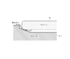
- the source gas supplied to the surface of the silicon wafer W in the epitaxial growth furnace passes through a slight gap between the edge on the back surface side of the silicon wafer W and the susceptor 33, so that the back surface of the wafer W is This causes silicon to deposit on the outer peripheral portion of the back surface of the silicon wafer W.
- the back surface silicon layer Eb is formed on the outer peripheral portion of the back surface S B of the silicon wafer W as shown in FIG. 12, the flatness of the outer peripheral portion of the back surface S B of the epitaxial silicon wafer EW is deteriorated.
- an object of the present invention is to provide an epitaxial wafer manufacturing method capable of easily manufacturing an epitaxial wafer having an improved back surface flatness.
- Another object of the present invention is to provide a double-side polishing method for a wafer capable of producing a silicon wafer suitable as a substrate material for such an epitaxial wafer and a double-side polishing carrier used therefor.
- the inventors of the present application have developed a method of preliminarily creating an edge roll-off on the back surface of the wafer in anticipation of the amount of epitaxial silicon deposited on the outer peripheral portion of the back surface of the wafer. It has been found that it is effective, and the deterioration of the flatness of the outer peripheral portion of the epitaxial wafer can be suppressed by offsetting the increase in the thickness of the outer peripheral portion of the wafer due to epitaxial growth with the edge roll-off.
- a method of adjusting the edge roll-off amount for example, a method of conditioning the polishing pad or changing the polishing pressure can be considered.
- the polishing pad conditioning or polishing pressure is changed to adjust the edge roll-off amount, it is also necessary to change the polishing recipe, and the polishing rate varies, so the global shape of the wafer changes and the desired quality Is difficult to secure, and has a negative effect on mass production.
- the present invention has been made on the basis of such technical knowledge, and the wafer double-side polishing method according to the present invention was disposed between an upper surface plate and a lower surface plate to which polishing cloths were respectively attached.
- a wafer is set in a holding hole of a double-side polishing carrier, and the upper and lower surface plates are rotated while the wafer and the double-side polishing carrier are sandwiched between the upper and lower surface plates.
- a method for polishing both sides of a wafer simultaneously wherein a chamfered portion is formed in at least one of an upper corner and a lower corner of the holding hole of the double-side polishing carrier,
- the edge roll-off on the back side of the wafer facing the direction where the chamfer is formed is larger than the edge roll-off on the front side of the wafer. Characterized by polishing the both sides of the wafer simultaneously.
- a desired edge roll-off can be intentionally formed on the back side of the wafer during the double-side polishing process of the wafer. Therefore, when this wafer is used as a substrate material for an epitaxial silicon wafer, the flatness of the final epitaxial wafer product after the formation of the epitaxial film can be increased.
- the height dimension of the chamfered portion of the double-side polishing carrier is preferably half or less of the thickness of the carrier.
- the width dimension of the chamfered portion of the double-sided polishing carrier is preferably equal to the height dimension of the chamfered portion, and both the height dimension and the width dimension of the chamfered portion are 0.2 mm or more and 0. It is especially preferable that it is 4 mm or less. According to this, a desired edge roll-off can be formed on the wafer while ensuring the wafer holding function of the carrier.
- the double-side polishing carrier includes a metal carrier body having a circular opening larger than the diameter of the wafer, and a ring-shaped resin inserter disposed along the inner periphery of the opening of the carrier body.
- the holding hole is an inner opening of the resin inserter, and the chamfered portion is formed in at least one of an upper corner and a lower corner of the inner opening of the resin inserter.
- the double-side polishing carrier comprises a resin carrier body having a circular opening, the opening of the carrier body serves as the holding hole, and the chamfered portion is formed in the opening.
- a desired edge roll-off can be formed on a wafer while ensuring a wafer holding function even in a resin-made double-side polishing carrier that does not use a resin inserter independent of the carrier body.
- the method for producing an epitaxial wafer according to the present invention includes forming a first epitaxial film on the entire surface of the wafer polished by the wafer double-side polishing method having the above characteristics, and A second epitaxial film is partially formed on the outer peripheral portion.
- the second epitaxial film preferably has a film thickness distribution that cancels edge roll-off on the back surface side of the wafer.
- the epitaxial wafer according to the present invention includes a wafer having a back surface side edge roll-off larger than the front surface side edge roll-off, a first epitaxial film formed on the entire surface of the wafer, and the back surface of the wafer. And the second epitaxial film partially formed on the outer peripheral portion of the wafer, and the flatness of the outer peripheral portion of the wafer on which the second epitaxial film is formed is such that the second epitaxial film is not formed. The flatness of the outer peripheral portion of the wafer is higher. ADVANTAGE OF THE INVENTION According to this invention, the epitaxial wafer with which the final flatness after film-forming of an epitaxial film was raised can be provided.
- the second epitaxial film preferably has a film thickness distribution that cancels edge roll-off on the back surface side of the wafer.
- the wafer is preferably a silicon wafer, and the first and second epitaxial films are preferably epitaxial silicon films. According to this, the flatness of the back surface of the epitaxial silicon wafer can be increased.
- the present invention it is possible to intentionally create a desired edge roll-off without greatly changing the polishing conditions, and thereby, near the edge of the final wafer product after the formation of the epitaxial film. It is possible to provide a double-side polishing carrier capable of increasing the flatness and a wafer polishing method using the same. Moreover, according to this invention, the manufacturing method of the epitaxial wafer which can raise the flatness of a back surface using the wafer grind
- FIG. 1 is a schematic side sectional view showing the structure of a double-side polishing apparatus according to an embodiment of the present invention.
- FIG. 2 is a plan view of the double-side polishing apparatus shown in FIG. 3A and 3B are diagrams showing the configuration of the carrier, where FIG. 3A is a plan view, FIG. 3B is a side sectional view, and FIG. 3C is a partially enlarged view near the inner peripheral surface of the holding hole.
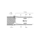
- FIG. 4 is a schematic diagram for explaining a mechanism for promoting edge roll-off by chamfering the carrier holding hole.
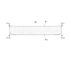
- FIG. 5 is a schematic cross-sectional view showing the shape of a silicon wafer after double-side polishing.
- FIG. 1 is a schematic side sectional view showing the structure of a double-side polishing apparatus according to an embodiment of the present invention.
- FIG. 2 is a plan view of the double-side polishing apparatus shown in FIG. 3A and 3B are diagrams showing the configuration of the carrier, where FIG. 3A is
- FIG. 6 is a schematic cross-sectional view showing an example of the configuration of an epitaxial growth apparatus used for manufacturing an epitaxial silicon wafer.
- FIG. 7 is a cross-sectional view of the epitaxial silicon wafer according to the present embodiment.
- FIG. 8 is a graph showing the relationship between the chamfered shape of the holding hole and the flatness of the wafer.
- FIGS. 9A and 9B are graphs showing the ZDD measurement results on the surface side of the sample wafer.
- FIGS. 10A and 10B are graphs showing the height profile on the back side of the epitaxial wafer.
- FIG. 11 is a schematic view for explaining the silicon deposition mechanism on the back side of the wafer in the epitaxial growth step.
- FIG. 12 is a schematic cross-sectional view showing the shape of a conventional epitaxial silicon wafer in which the flatness of the outer peripheral portion of the back surface has deteriorated.
- FIG. 1 is a schematic side sectional view showing a configuration of a double-side polishing apparatus according to an embodiment of the present invention.
- 2 is a plan view of the double-side polishing apparatus shown in FIG. 1, and
- FIG. 1 is a cross-sectional view taken along the line RR ′ of FIG.
- the double-side polishing apparatus 1 includes an upper surface plate 2 and a lower surface plate 3 that are provided facing each other in the vertical direction. Polishing cloths 4 and 5 are respectively attached to the upper surface. A sun gear 6 is provided at the center between the upper surface plate 2 and the lower surface plate 3, and an internal gear 7 is provided at the peripheral portion. The silicon wafer W is sandwiched between the upper surface plate 2 and the lower surface plate 3 while being set in the holding hole 10 a of the double-side polishing carrier 10.
- each carrier 10 is provided around the sun gear 6, and the outer peripheral teeth 10 b of each carrier 10 are engaged with the tooth portions of the sun gear 6 and the internal gear 7.
- Each of the carriers 10 revolves around the sun gear 6 while rotating as the board 2 and the lower platen 3 are driven to rotate by a drive source (not shown).
- the silicon wafer W set in the holding hole 10a of the carrier 10 is held by the carrier 10, and both surfaces thereof are simultaneously polished by contact with the upper and lower polishing cloths 4 and 5.
- a polishing liquid is supplied from a nozzle (not shown).
- the polishing liquid for example, an alkaline solution in which colloidal silica is dispersed can be used.
- FIG. 3A and 3B are diagrams illustrating the configuration of the carrier 10, where FIG. 3A is a plan view, FIG. 3B is a side cross-sectional view, and FIG. .
- the carrier 10 includes a metal carrier body 11 having a circular opening 11 a larger than the silicon wafer W, and an inner periphery of the opening 11 a of the carrier body 11.
- a ring-shaped resin inserter 12 is provided.
- the carrier body 11 is a disk-shaped member, and outer peripheral teeth 11b are provided on the outer peripheral portion.
- a typical material of the carrier body 11 is SUS, but other metal materials such as titanium may be used.
- the thickness D of the carrier body 11 is set based on the target thickness of the wafer W after double-side polishing. For example, the thickness of the carrier 10 for a 300 mm diameter wafer is set to 0.8 mm, and the thickness of the wafer W before processing is about 1 mm. Sizing is performed to reduce the thickness of the carrier to the same level as the carrier 10. Since the center position of the opening 11 a is offset from the center position of the carrier body 11, the wafer W set in the opening 11 a moves eccentrically with the center of the carrier body 11 as the rotation axis. Uniformity is improved.
- the resin inserter 12 is interposed between the outer peripheral surface of the wafer W and the inner peripheral surface of the opening 11a of the carrier body 11, and plays a role of preventing contact between the two.
- the inner opening 12 a of the resin inserter 12 forms a holding hole 10 a (see FIG. 2) of the carrier 10, and the outer peripheral surface of the wafer W is in contact with the inner peripheral surface of the resin inserter 12.
- the lateral width (ring width) of the resin inserter 12 is 1.5 mm, for example, and is determined in consideration of the size of the opening 11a of the carrier body 11 and the size of the wafer W.
- the thickness of the resin inserter 12 is preferably the same as the thickness D of the carrier body 11.
- chamfered portion 12c is formed in the lower corner C CB of the inner peripheral portion of the inner opening 12a of the resin inserter 12 .
- the lower corner C CB of the inner peripheral surface of the inner opening 12a of the resin inserter 12 is chamfered, only the upper corner C CF may be chamfered. That is, it is only necessary that the chamfered portion 12 c is formed at one of the upper and lower corners of the inner peripheral portion of the wafer holding hole 10 a of the carrier 10.
- the edge roll-off on one side of the wafer W can be intentionally increased by providing such a chamfer in the wafer holding hole 10a.
- height h 1 and width h 2 of the chamfered portion 12c is both 0.1mm or more.
- the height h 1 and width h 2 is less than 0.1mm can not be obtained the effect of providing the chamfered portion 12c, moreover chamfering from the viewpoint of processing accuracy because very difficult.
- the height h 1 of the chamfered portion 12c is preferably a half or less of the thickness D of the carrier 10 (D ⁇ h 1/2 ), the width h 2 is equal to or less than the width of the resin inserter 12 .
- the height h 1 of the chamfered portion 12c when the thickness of the carrier 10 is 0.8mm is 0.4mm or less
- the chamfered portion when the width of the resin inserter 12 is 1.5mm width h 2 of 12c is preferably at 1.5mm or less.
- the height h 1 of the chamfered portion 12c is larger than half the thickness D of the carrier 10 is too edge roll-off amount is large after the formation of the epitaxial film is because not be ensured a desired flatness, This is because the function of holding the wafer W may be hindered.
- the width h 2 of the chamfered portion 12c is larger than the width of the resin inserter 12 is decreased the thickness of the resin inserter 12, thereby because the edge roll off of the wafer W is increased.
- the chamfered portion 12c is particularly preferably a C0.2 to C0.4 chamfer.
- the chamfer angle 45 degrees to align the chamfer height h 1 and width h 2 of 12c it is possible to enhance the machining accuracy and ease of chamfering.
- the amount of silicon deposited on the back surface of the wafer in the epitaxial process is offset. A large edge roll-off can be created.
- FIG. 4 is a schematic diagram for explaining a mechanism for promoting edge roll-off by chamfering the holding hole 10 a of the carrier 10.
- the edge roll-off of the wafer W is improved by the retainer effect (reaction force against the polishing cloth) of the carrier 10 as in the case of the conventional carrier.
- the flatness of the outer peripheral part is increased.
- the retainer effect is reduced by the presence of the chamfered portion 12c, the effect of improving the edge roll-off is suppressed, the outer peripheral portion of the wafer W
- the flatness of the is reduced.
- the upward arrow in the figure indicates that the reaction force of the carrier 10 with respect to the polishing cloth 4 is large, and the downward arrow indicates that the reaction force of the carrier 10 with respect to the polishing cloth 5 is small.
- FIG. 5 is a schematic cross-sectional view showing the shape of the silicon wafer W after double-side polishing.
- the outer peripheral portion shape of the silicon wafer W after the double-side polishing As shown in FIG. 5, the outer peripheral portion shape of the silicon wafer W after the double-side polishing, the surface S F side corner C WF edge roll-off of small, large roll-off corner C WB of the back S B side.
- a wafer W as a substrate material for epitaxial silicon wafer, it is possible to offset the increase in thickness of silicon is deposited on the outer periphery of the rear surface S B of the wafer W, the outer peripheral portion of the back surface of the epitaxial silicon wafer The flatness of can be increased.
- FIG. 6 is a schematic cross-sectional view showing an example of the configuration of an epitaxial growth apparatus used for manufacturing an epitaxial silicon wafer.
- the epitaxial growth apparatus 30 is a single-wafer type apparatus that processes silicon wafers W one by one, and includes a chamber 31 made of quartz glass and a lid member 32 that covers the top of the chamber 31. I have.
- a susceptor 33 and a preheating ring 34 for supporting a wafer are provided in the chamber 31, and the susceptor 33 is supported by a support shaft 35.
- a gas inlet 36, a baffle 37, and a rectifying member 38 are provided on one side of the chamber 31, and a gas outlet 39 is provided on the other end facing the chamber 31.
- An upper lamp 40 for heating the silicon wafer W placed on the susceptor 33 is provided above the lid member 32.
- a lower lamp 41 that heats the silicon wafer W from below is provided below the susceptor 33.
- a source gas such as trichlorosilane (SiHCl 3 ) or dichlorosilane (SiH 2 Cl 2 ) is introduced into the chamber 31 from the gas inlet 36 while exhausting from the gas outlet 39.
- the raw material gas flows from the gas introduction port 36 through the baffle 37 and the rectifying member 38 into the upper space 31 a of the chamber 31.
- the wafer W, the susceptor 33 and the preheating ring 34 are heated by the upper lamp 40 and the lower lamp 41, and the source gas flows in a laminar state along the surface of the heated wafer W, so that the epitaxial growth occurs on the surface of the wafer W. Occurs and an epitaxial film is formed.
- the edge on the back surface side of the silicon wafer W is in line contact with the surface of the susceptor 33, but there is a very small gap formed by slight unevenness between them.
- silicon is deposited on the outer periphery of the back side of the wafer W.
- the silicon deposition on the outer peripheral portion of the wafer W is offset by the edge roll-off on the rear surface of the wafer, and the outer peripheral portion of the rear surface becomes a flat shape. Therefore, even when silicon is deposited on the outer peripheral portion of the rear surface of the wafer W, The flatness of the back surface does not deteriorate.
- FIG. 7 is a cross-sectional view of the epitaxial silicon wafer according to the present embodiment.
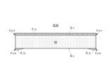
- an epitaxial silicon wafer EW includes a back surface S B side of the edge roll-off surface S F greater than side silicon wafer W (see FIG. 5), formed on the entire surface S F of the silicon wafer W
- the epitaxial silicon film Ea is provided. Also on the outer peripheral portion of the back surface S B of the silicon wafer W backside silicon film Eb it is partially deposited.
- backside silicon film Eb to offset the rear surface S B side of the edge roll-off of the silicon wafer W is formed with a suitable thickness distribution, the flatness of the outer peripheral portion of the back surface side of the epitaxial silicon wafer EW Enhanced.
- the double-side polishing carrier 10 is provided with the chamfered portion 12c at the corner of the holding hole 10a, and therefore, a predetermined amount of edge roll-off is applied to the outer peripheral portion of the wafer W after double-side polishing. Can be deliberately built.
- the epitaxial wafer EW is manufactured using the wafer W whose edge roll-off on one side is adjusted in this way, a phenomenon in which epitaxial silicon is deposited on the outer peripheral portion of the back surface and the thickness of the outer peripheral portion increases more than necessary. And the flatness of the outer peripheral portion of the back surface of the epitaxial silicon wafer EW can be increased.
- the carrier 10 is configured by the metal carrier body 11 and the resin inserter 12 has been described as an example.
- the carrier body 11 is made of resin and the resin inserter 12 is omitted. May be.
- the opening 11a of the carrier body 11 becomes the wafer holding hole 10a, and the corner of the opening 11a of the carrier body 11 is chamfered.
- one carrier 10 has one holding hole 10a and holds one wafer W, but one carrier 10 may have a plurality of holding holes. In this case, chamfering is performed on each of the plurality of holding holes.
- the configuration of the double-side polishing apparatus 1 according to the present embodiment is an example, and various types can be employed.
- the present invention is limited to double-side polishing of a silicon wafer. It can be used for double-side polishing of various wafers.
- GBIR is an index indicating the global flatness of the wafer
- ESFQD is an index indicating the site flatness at the outer peripheral portion (edge) of the wafer.
- ESFQD divides the outer periphery of a wafer into a large number (for example, 72) of fan-shaped regions (sites), and uses the in-site plane calculated from the data in the site by the method of least squares as a reference. Each site has one data. That is, ESFQD is the SFQD value of each site (positive or negative larger deviation from the least square surface in the region).
- the ESFQD site excludes a region 2 mm in the diametrical direction from the outermost periphery, two straight lines with a sector length of 30 mm extending from the inner peripheral reference end to the radially central side, and a wafer outer peripheral direction of 5 °. This is a substantially rectangular area surrounded by an arc corresponding to ( ⁇ 2.5 °).
- FIG. 8 is a graph showing the relationship between the chamfered shape of the holding hole and the flatness of the wafer, where the horizontal axis represents the global shape (Global shape) and the vertical axis represents the ESFQD.
- the squares in the figure indicate regions that satisfy both the global shape and ESFQD target ranges.
- the global shape is a GBIR value considering the concept of unevenness. That is, looking at the profile (overall shape) of GBIR measurement results, the value of GBIR is plotted on the horizontal axis as a plus side if it is a convex shape (Convex) and as a minus side if it is a concave shape (Concave). is there.
- ZDD Z-height double differential
- 9 (a) and 9 (b) are graphs showing the measurement results of the ZDD on the front side and the back side of the sample wafer.
- the ZDD on the front side of the wafer was the same in all of the comparative example, the example 1, and the example 2, and the results were almost unchanged.
- FIG. 9B it was found that the ZDD on the back surface side of the wafer was the smallest in the comparative example and increased in the order of Example 1 and Example 2.
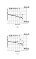
- FIGS. 10A and 10B are graphs showing the height profile on the back side of the epitaxial wafer EW, where the horizontal axis is the radial distance (mm) from the wafer center, and the vertical axis is the height from the reference plane. (Nm) is shown respectively.
- FIG. 10A shows the flatness of the wafer of the comparative example
- FIG. 10B shows the flatness of the wafer of Example 1.
- the line A is the height profile on the back side of the wafer EW before epitaxial growth
- the line B is the height profile on the back side of the wafer EW after epitaxial growth
- the line C is the wafer after epitaxial growth.
- the profile of the silicon deposition amount on the back side of the EW is shown.
- the height profile A on the back side of the wafer EW before the formation of the epitaxial film is higher than that of the comparative example (FIG. 10A) in Example 1 (FIG. 10B).
- the height profile B on the back surface side of the wafer EW after the formation of the epitaxial film is a comparative example (FIG. 10A) because the deposition of the back surface epitaxial film offsets the edge roll-off. ))
- the flatness of Example 1 (FIG. 10B) was higher.
Landscapes
- Engineering & Computer Science (AREA)
- Mechanical Engineering (AREA)
- Mechanical Treatment Of Semiconductor (AREA)
- Finish Polishing, Edge Sharpening, And Grinding By Specific Grinding Devices (AREA)
Abstract
Description
2 上定盤
3 下定盤
4 研磨布
5 研磨布
6 サンギヤ
7 インターナルギヤ
10 両面研磨用キャリア
10a 保持孔(ウェーハ保持孔)
10bキャリアの外周歯
11 キャリア本体
11a キャリア本体の開口
11b キャリア本体の外周歯(キャリアの外周歯)
12 樹脂インサータ
12a 樹脂インサータの内側開口
12c 面取り部
30 エピタキシャル成長装置
31 チャンバー
31a 上部空間
32 蓋部材
33 サセプター
34 予熱リング
35 支持シャフト
36 ガス導入口
37 バッフル
38 整流部材
39 ガス排出口
40 上部ランプ
41 下部ランプ
CCB 保持孔の下側コーナー
CCF 保持孔の上側コーナー
CWB ウェーハの上側コーナー
CWF ウェーハの下側コーナー
Ea エピタキシャルシリコン膜
Eb 裏面シリコン膜
EW エピタキシャルシリコンウェーハ(エピタキシャルウェーハ)
h1 面取り部の高さ寸法
h2 面取り部の幅寸法
SB ウェーハの裏面
SF ウェーハの表面
W シリコンウェーハ(基板材料)
Claims (12)
- 研磨布がそれぞれ貼り付けられた上定盤と下定盤との間に配設された両面研磨用キャリアの保持孔内にウェーハをセットし、前記ウェーハおよび前記両面研磨用キャリアを前記上定盤と前記下定盤で挟み込んだ状態で前記上定盤および前記下定盤を回転させて前記ウェーハの両面を同時に研磨するウェーハの両面研磨方法であって、
前記両面研磨用キャリアの前記保持孔の上側コーナーおよび下側コーナーの少なくとも一方に面取り部が形成されており、
前記両面研磨用キャリアの前記面取り部が形成されている方を向いた前記ウェーハの裏面側のエッジロールオフが前記ウェーハの表面側のエッジロールオフよりも大きくなるように前記ウェーハの両面を同時に研磨することを特徴とするウェーハの両面研磨方法。 - 前記両面研磨用キャリアの前記面取り部の高さ寸法は当該キャリアの厚みの半分以下である、請求項1に記載のウェーハの両面研磨方法。
- 前記両面研磨用キャリアの前記面取り部の幅寸法は前記面取り部の前記高さ寸法と等しい、請求項2に記載のウェーハの両面研磨方法。
- 前記両面研磨用キャリアの前記面取り部の前記高さ寸法および前記幅寸法はともに0.2mm以上0.4mm以下である、請求項3に記載のウェーハの両面研磨方法。
- 前記両面研磨用キャリアは、
前記ウェーハの直径よりも大きな円形の開口を有する金属製のキャリア本体と、
前記キャリア本体の前記開口の内周に沿って配置されたリング状の樹脂インサータとを備え、
前記保持孔は前記樹脂インサータの内側開口からなり、
前記樹脂インサータに前記面取り部が形成されている、請求項1ないし4のいずれか一項に記載のウェーハの両面研磨方法。 - 前記両面研磨用キャリアは、
円形の開口を有する樹脂製のキャリア本体からなり、前記キャリア本体の前記開口が前記保持孔となり、前記開口に前記面取り部が形成されている、請求項1ないし4のいずれか一項に記載のウェーハの両面研磨方法。 - 請求項1乃至6のいずれか一項に記載のウェーハの両面研磨方法によって研磨加工された前記ウェーハの前記表面の全面に第1のエピタキシャル膜を形成すると共に、前記ウェーハの前記裏面の外周部に第2のエピタキシャル膜を部分的に形成することを特徴とするエピタキシャルウェーハの製造方法。
- 前記第2のエピタキシャル膜は、前記ウェーハの裏面側のエッジロールオフを相殺する膜厚分布を有する、請求項7に記載のエピタキシャルウェーハの製造方法。
- 前記ウェーハはシリコンウェーハであり、
前記第1及び第2のエピタキシャル膜はエピタキシャルシリコン膜である、請求項7又は8に記載のエピタキシャルウェーハの製造方法。 - 裏面側のエッジロールオフが表面側のエッジロールオフよりも大きいウェーハと、
前記ウェーハの表面の全面に形成された第1のエピタキシャル膜と、
前記ウェーハの裏面の外周部に部分的に形成された第2のエピタキシャル膜とを備え、
前記第2のエピタキシャル膜が形成された前記ウェーハの外周部の平坦度は、前記第2のエピタキシャル膜が形成されていない前記ウェーハの外周部の平坦度よりも高いことを特徴とするエピタキシャルウェーハ。 - 前記第2のエピタキシャル膜は、前記ウェーハの裏面側のエッジロールオフを相殺する膜厚分布を有する、請求項10に記載のエピタキシャルウェーハ。
- 前記ウェーハはシリコンウェーハであり、
前記第1及び第2のエピタキシャル膜はエピタキシャルシリコン膜である、請求項10又は11に記載のエピタキシャルウェーハ。
Priority Applications (3)
| Application Number | Priority Date | Filing Date | Title |
|---|---|---|---|
| CN201680075581.2A CN108602173B (zh) | 2015-12-22 | 2016-11-04 | 晶圆的双面抛光方法及使用该双面抛光方法的外延晶圆的制造方法以及外延晶圆 |
| DE112016005920.5T DE112016005920B4 (de) | 2015-12-22 | 2016-11-04 | Verfahren zum beidseitigen Polieren eines Wafers, Verfahren zum Herstellen eines Epitaxialwafers und Verwendung desselben sowie Epitaxialwafer |
| KR1020187017434A KR102090588B1 (ko) | 2015-12-22 | 2016-11-04 | 웨이퍼의 양면 연마 방법 및 이것을 이용한 에피택셜 웨이퍼의 제조 방법 그리고 에피택셜 웨이퍼 |
Applications Claiming Priority (2)
| Application Number | Priority Date | Filing Date | Title |
|---|---|---|---|
| JP2015249312A JP6128198B1 (ja) | 2015-12-22 | 2015-12-22 | ウェーハの両面研磨方法及びこれを用いたエピタキシャルウェーハの製造方法 |
| JP2015-249312 | 2015-12-22 |
Publications (1)
| Publication Number | Publication Date |
|---|---|
| WO2017110262A1 true WO2017110262A1 (ja) | 2017-06-29 |
Family
ID=58714814
Family Applications (1)
| Application Number | Title | Priority Date | Filing Date |
|---|---|---|---|
| PCT/JP2016/082764 Ceased WO2017110262A1 (ja) | 2015-12-22 | 2016-11-04 | ウェーハの両面研磨方法及びこれを用いたエピタキシャルウェーハの製造方法並びにエピタキシャルウェーハ |
Country Status (6)
| Country | Link |
|---|---|
| JP (1) | JP6128198B1 (ja) |
| KR (1) | KR102090588B1 (ja) |
| CN (1) | CN108602173B (ja) |
| DE (1) | DE112016005920B4 (ja) |
| TW (1) | TWI618601B (ja) |
| WO (1) | WO2017110262A1 (ja) |
Cited By (1)
| Publication number | Priority date | Publication date | Assignee | Title |
|---|---|---|---|---|
| CN110350020A (zh) * | 2018-04-03 | 2019-10-18 | 环球晶圆股份有限公司 | 外延基板 |
Families Citing this family (16)
| Publication number | Priority date | Publication date | Assignee | Title |
|---|---|---|---|---|
| JP6579056B2 (ja) * | 2016-07-29 | 2019-09-25 | 株式会社Sumco | ウェーハの両面研磨方法 |
| DE102017210423A1 (de) * | 2017-06-21 | 2018-12-27 | Siltronic Ag | Verfahren, Steuerungssystem und Anlage zum Bearbeiten einer Halbleiterscheibe sowie Halbleiterscheibe |
| DE102018202059A1 (de) * | 2018-02-09 | 2019-08-14 | Siltronic Ag | Verfahren zum Polieren einer Halbleiterscheibe |
| DE112019004610T5 (de) * | 2018-09-14 | 2021-09-02 | Sumco Corporation | Waferhochglanzabschrägverfahren, verfahren zur herstellung von wafern und wafer |
| CN109551311A (zh) * | 2018-12-12 | 2019-04-02 | 大连理工大学 | 一种机械研磨或抛光过程中减小塌边现象的方法 |
| CN109514370B (zh) * | 2018-12-20 | 2020-04-14 | 象山谢海家具有限公司 | 木床用板材表面打磨装置 |
| CN110010458B (zh) * | 2019-04-01 | 2021-08-27 | 徐州鑫晶半导体科技有限公司 | 控制半导体晶圆片表面形貌的方法和半导体晶片 |
| CN113644017B (zh) * | 2020-04-27 | 2024-07-09 | 上海新昇半导体科技有限公司 | 一种对晶圆进行定位的方法和半导体制造设备 |
| CN111599673A (zh) * | 2020-06-03 | 2020-08-28 | 福建阿石创新材料股份有限公司 | 一种钼晶圆片的磨抛方法 |
| JP2023061759A (ja) * | 2021-10-20 | 2023-05-02 | スピードファム株式会社 | ワークキャリア |
| CN218351409U (zh) * | 2022-06-30 | 2023-01-20 | 苏州晶湛半导体有限公司 | 一种半导体结构 |
| CN115847281A (zh) * | 2022-12-07 | 2023-03-28 | 西安奕斯伟材料科技有限公司 | 一种硅片的双面抛光用的载具以及装置 |
| CN115990825A (zh) * | 2022-12-27 | 2023-04-21 | 西安奕斯伟材料科技股份有限公司 | 一种硅片双面抛光用的载具、双面抛光装置及硅片 |
| CN115816267B (zh) * | 2022-12-29 | 2025-03-21 | 西安奕斯伟材料科技股份有限公司 | 硅片双面抛光装置的承载件及硅片双面抛光装置 |
| CN116551559B (zh) * | 2023-02-28 | 2023-12-12 | 名正(浙江)电子装备有限公司 | 一种带压力传感系统的晶圆研磨抛光机 |
| CN118700014A (zh) * | 2024-07-16 | 2024-09-27 | 河北同光半导体股份有限公司 | 一种晶圆研磨抛光设备及研磨抛光方法 |
Citations (4)
| Publication number | Priority date | Publication date | Assignee | Title |
|---|---|---|---|---|
| JPH07156062A (ja) * | 1993-11-30 | 1995-06-20 | Kyushu Komatsu Denshi Kk | ラッピングキャリア |
| WO2006001340A1 (ja) * | 2004-06-23 | 2006-01-05 | Komatsu Denshi Kinzoku Kabushiki Kaisha | 両面研磨用キャリアおよびその製造方法 |
| JP2012109310A (ja) * | 2010-11-15 | 2012-06-07 | Sumco Corp | エピタキシャルウェーハの製造方法およびエピタキシャルウェーハ |
| JP2015104771A (ja) * | 2013-11-29 | 2015-06-08 | Hoya株式会社 | 磁気ディスク用ガラス基板の製造方法及び研磨処理用キャリア |
Family Cites Families (7)
| Publication number | Priority date | Publication date | Assignee | Title |
|---|---|---|---|---|
| JP3791302B2 (ja) * | 2000-05-31 | 2006-06-28 | 株式会社Sumco | 両面研磨装置を用いた半導体ウェーハの研磨方法 |
| JP4904960B2 (ja) | 2006-07-18 | 2012-03-28 | 信越半導体株式会社 | 両面研磨装置用キャリア及びこれを用いた両面研磨装置並びに両面研磨方法 |
| JP5151800B2 (ja) * | 2008-08-20 | 2013-02-27 | 信越半導体株式会社 | 両面研磨装置用キャリア及びこれを用いた両面研磨装置並びに両面研磨方法 |
| JP5326888B2 (ja) | 2009-07-13 | 2013-10-30 | 株式会社Sumco | エピタキシャルウェーハの製造方法 |
| JP5402657B2 (ja) * | 2010-01-14 | 2014-01-29 | 株式会社Sumco | エピタキシャル成長装置 |
| JP5648623B2 (ja) * | 2011-12-01 | 2015-01-07 | 信越半導体株式会社 | 両面研磨装置用キャリア及びこれを用いた両面研磨装置並びに両面研磨方法 |
| JP5748717B2 (ja) * | 2012-09-06 | 2015-07-15 | 信越半導体株式会社 | 両面研磨方法 |
-
2015
- 2015-12-22 JP JP2015249312A patent/JP6128198B1/ja active Active
-
2016
- 2016-11-04 WO PCT/JP2016/082764 patent/WO2017110262A1/ja not_active Ceased
- 2016-11-04 CN CN201680075581.2A patent/CN108602173B/zh active Active
- 2016-11-04 KR KR1020187017434A patent/KR102090588B1/ko active Active
- 2016-11-04 DE DE112016005920.5T patent/DE112016005920B4/de active Active
- 2016-11-07 TW TW105136097A patent/TWI618601B/zh active
Patent Citations (4)
| Publication number | Priority date | Publication date | Assignee | Title |
|---|---|---|---|---|
| JPH07156062A (ja) * | 1993-11-30 | 1995-06-20 | Kyushu Komatsu Denshi Kk | ラッピングキャリア |
| WO2006001340A1 (ja) * | 2004-06-23 | 2006-01-05 | Komatsu Denshi Kinzoku Kabushiki Kaisha | 両面研磨用キャリアおよびその製造方法 |
| JP2012109310A (ja) * | 2010-11-15 | 2012-06-07 | Sumco Corp | エピタキシャルウェーハの製造方法およびエピタキシャルウェーハ |
| JP2015104771A (ja) * | 2013-11-29 | 2015-06-08 | Hoya株式会社 | 磁気ディスク用ガラス基板の製造方法及び研磨処理用キャリア |
Cited By (2)
| Publication number | Priority date | Publication date | Assignee | Title |
|---|---|---|---|---|
| CN110350020A (zh) * | 2018-04-03 | 2019-10-18 | 环球晶圆股份有限公司 | 外延基板 |
| CN110350020B (zh) * | 2018-04-03 | 2022-11-08 | 环球晶圆股份有限公司 | 外延基板 |
Also Published As
| Publication number | Publication date |
|---|---|
| JP2017113816A (ja) | 2017-06-29 |
| KR20180084126A (ko) | 2018-07-24 |
| DE112016005920B4 (de) | 2025-06-12 |
| TW201729941A (zh) | 2017-09-01 |
| CN108602173B (zh) | 2020-08-11 |
| JP6128198B1 (ja) | 2017-05-17 |
| DE112016005920T5 (de) | 2018-09-13 |
| TWI618601B (zh) | 2018-03-21 |
| CN108602173A (zh) | 2018-09-28 |
| KR102090588B1 (ko) | 2020-03-18 |
Similar Documents
| Publication | Publication Date | Title |
|---|---|---|
| JP6128198B1 (ja) | ウェーハの両面研磨方法及びこれを用いたエピタキシャルウェーハの製造方法 | |
| KR101077324B1 (ko) | 에피택셜 코팅 실리콘 웨이퍼의 제조 방법 | |
| CN1936110B (zh) | 外延涂覆的硅晶片以及制造外延涂覆的硅晶片的方法 | |
| TWI424476B (zh) | 磊晶塗覆的矽晶圓及製造磊晶塗覆的矽晶圓的方法 | |
| TWI420003B (zh) | 經磊晶塗覆的矽晶圓的製造方法 | |
| CN104756244A (zh) | 用于外延生长的衬托器和用于外延生长的方法 | |
| JP6697558B2 (ja) | 半導体ウェハをエピタキシャル被覆するための方法 | |
| US10513797B2 (en) | Manufacturing method of epitaxial silicon wafer | |
| TWI419255B (zh) | Epitaxial growth | |
| WO2018020798A1 (ja) | ウェーハの両面研磨方法 | |
| CN111295737B (zh) | 基座、外延生长装置、外延硅晶片的制造方法及外延硅晶片 | |
| JP5472073B2 (ja) | 半導体ウェーハ及びその製造方法 | |
| JP5326888B2 (ja) | エピタキシャルウェーハの製造方法 | |
| TWI445053B (zh) | Epitaxy growth method | |
| JP4899445B2 (ja) | エピタキシャルウェーハの製造方法及びエピタキシャルウェーハ | |
| WO2019098033A1 (ja) | サセプタ、エピタキシャルウェーハの製造方法 | |
| JP2020191346A (ja) | サセプタおよびエピタキシャル成長装置 | |
| CN207362367U (zh) | 外延涂覆的硅晶片 | |
| US8664123B2 (en) | Method for manufacturing nitride semiconductor substrate | |
| JP2010040574A (ja) | エピタキシャルウェーハの製造方法およびエピタキシャルウェーハ | |
| JP5206613B2 (ja) | エピタキシャルウェーハ用サセプタ、およびその製造方法、並びにそれを用いたエピタキシャル成長装置 |
Legal Events
| Date | Code | Title | Description |
|---|---|---|---|
| 121 | Ep: the epo has been informed by wipo that ep was designated in this application |
Ref document number: 16878160 Country of ref document: EP Kind code of ref document: A1 |
|
| ENP | Entry into the national phase |
Ref document number: 20187017434 Country of ref document: KR Kind code of ref document: A |
|
| WWE | Wipo information: entry into national phase |
Ref document number: 1020187017434 Country of ref document: KR |
|
| WWE | Wipo information: entry into national phase |
Ref document number: 112016005920 Country of ref document: DE |
|
| 122 | Ep: pct application non-entry in european phase |
Ref document number: 16878160 Country of ref document: EP Kind code of ref document: A1 |
|
| WWG | Wipo information: grant in national office |
Ref document number: 112016005920 Country of ref document: DE |