WO2017086112A1 - 導電性高分子用インビジブルエッチングインクおよび導電性高分子のパターニング方法 - Google Patents
導電性高分子用インビジブルエッチングインクおよび導電性高分子のパターニング方法 Download PDFInfo
- Publication number
- WO2017086112A1 WO2017086112A1 PCT/JP2016/081798 JP2016081798W WO2017086112A1 WO 2017086112 A1 WO2017086112 A1 WO 2017086112A1 JP 2016081798 W JP2016081798 W JP 2016081798W WO 2017086112 A1 WO2017086112 A1 WO 2017086112A1
- Authority
- WO
- WIPO (PCT)
- Prior art keywords
- conductive polymer
- etching
- ink
- invisible
- film
- Prior art date
- Legal status (The legal status is an assumption and is not a legal conclusion. Google has not performed a legal analysis and makes no representation as to the accuracy of the status listed.)
- Ceased
Links
Classifications
-
- C—CHEMISTRY; METALLURGY
- C09—DYES; PAINTS; POLISHES; NATURAL RESINS; ADHESIVES; COMPOSITIONS NOT OTHERWISE PROVIDED FOR; APPLICATIONS OF MATERIALS NOT OTHERWISE PROVIDED FOR
- C09D—COATING COMPOSITIONS, e.g. PAINTS, VARNISHES OR LACQUERS; FILLING PASTES; CHEMICAL PAINT OR INK REMOVERS; INKS; CORRECTING FLUIDS; WOODSTAINS; PASTES OR SOLIDS FOR COLOURING OR PRINTING; USE OF MATERIALS THEREFOR
- C09D11/00—Inks
- C09D11/02—Printing inks
- C09D11/10—Printing inks based on artificial resins
-
- C—CHEMISTRY; METALLURGY
- C09—DYES; PAINTS; POLISHES; NATURAL RESINS; ADHESIVES; COMPOSITIONS NOT OTHERWISE PROVIDED FOR; APPLICATIONS OF MATERIALS NOT OTHERWISE PROVIDED FOR
- C09D—COATING COMPOSITIONS, e.g. PAINTS, VARNISHES OR LACQUERS; FILLING PASTES; CHEMICAL PAINT OR INK REMOVERS; INKS; CORRECTING FLUIDS; WOODSTAINS; PASTES OR SOLIDS FOR COLOURING OR PRINTING; USE OF MATERIALS THEREFOR
- C09D11/00—Inks
- C09D11/02—Printing inks
- C09D11/10—Printing inks based on artificial resins
- C09D11/106—Printing inks based on artificial resins containing macromolecular compounds obtained by reactions only involving carbon-to-carbon unsaturated bonds
- C09D11/107—Printing inks based on artificial resins containing macromolecular compounds obtained by reactions only involving carbon-to-carbon unsaturated bonds from unsaturated acids or derivatives thereof
-
- C—CHEMISTRY; METALLURGY
- C09—DYES; PAINTS; POLISHES; NATURAL RESINS; ADHESIVES; COMPOSITIONS NOT OTHERWISE PROVIDED FOR; APPLICATIONS OF MATERIALS NOT OTHERWISE PROVIDED FOR
- C09D—COATING COMPOSITIONS, e.g. PAINTS, VARNISHES OR LACQUERS; FILLING PASTES; CHEMICAL PAINT OR INK REMOVERS; INKS; CORRECTING FLUIDS; WOODSTAINS; PASTES OR SOLIDS FOR COLOURING OR PRINTING; USE OF MATERIALS THEREFOR
- C09D11/00—Inks
- C09D11/02—Printing inks
- C09D11/03—Printing inks characterised by features other than the chemical nature of the binder
-
- H—ELECTRICITY
- H01—ELECTRIC ELEMENTS
- H01B—CABLES; CONDUCTORS; INSULATORS; SELECTION OF MATERIALS FOR THEIR CONDUCTIVE, INSULATING OR DIELECTRIC PROPERTIES
- H01B1/00—Conductors or conductive bodies characterised by the conductive materials; Selection of materials as conductors
- H01B1/06—Conductors or conductive bodies characterised by the conductive materials; Selection of materials as conductors mainly consisting of other non-metallic substances
- H01B1/12—Conductors or conductive bodies characterised by the conductive materials; Selection of materials as conductors mainly consisting of other non-metallic substances organic substances
- H01B1/124—Intrinsically conductive polymers
- H01B1/127—Intrinsically conductive polymers comprising five-membered aromatic rings in the main chain, e.g. polypyrroles, polythiophenes
-
- H—ELECTRICITY
- H01—ELECTRIC ELEMENTS
- H01B—CABLES; CONDUCTORS; INSULATORS; SELECTION OF MATERIALS FOR THEIR CONDUCTIVE, INSULATING OR DIELECTRIC PROPERTIES
- H01B1/00—Conductors or conductive bodies characterised by the conductive materials; Selection of materials as conductors
- H01B1/06—Conductors or conductive bodies characterised by the conductive materials; Selection of materials as conductors mainly consisting of other non-metallic substances
- H01B1/12—Conductors or conductive bodies characterised by the conductive materials; Selection of materials as conductors mainly consisting of other non-metallic substances organic substances
- H01B1/124—Intrinsically conductive polymers
- H01B1/128—Intrinsically conductive polymers comprising six-membered aromatic rings in the main chain, e.g. polyanilines, polyphenylenes
-
- H—ELECTRICITY
- H01—ELECTRIC ELEMENTS
- H01B—CABLES; CONDUCTORS; INSULATORS; SELECTION OF MATERIALS FOR THEIR CONDUCTIVE, INSULATING OR DIELECTRIC PROPERTIES
- H01B13/00—Apparatus or processes specially adapted for manufacturing conductors or cables
Definitions
- the present invention relates to an invisible etching ink for a conductive polymer and a conductive polymer patterning method using the ink.
- ITO indium tin oxide
- indium is a rare element
- Conductive polymers are characterized by conductivity, light transmission, light emission, and flexibility after film formation, and can be applied to transparent conductive films, electrolytic capacitors, antistatic agents, batteries, and organic EL devices. Expected.
- the conductive polymer is a useful material for the electronics industry, and is particularly expected as a transparent material for the sensor part of touch panels and touch switches. Therefore, the method of etching the conductive polymer and patterning the conductive polymer film is an important technique in using the conductive polymer.
- Resistive touch panels for consumer use are mainly resistive and capacitive, and are further subdivided according to the detection method. It is necessary to form an electrode pattern for detection on the digital type resistive touch panel and the projection type capacitive touch panel. Since the transparent conductive material containing ITO is not completely colorless, the formed pattern is visible on the screen, which affects the color tone of the image.
- the etched part is required to maintain the color tone before etching.
- the PEDOT / PSS film is light blue, if the etched portion can maintain the original color tone of the film, there is an advantage that a pattern cannot be seen on the screen even if it is mounted on a capacitive touch panel.
- a layer containing 10 to 5000 mg / m 2 of a conductive polymer is applied on a support to form a conductive layer.
- ClO -, BrO - method for printing an electrode pattern on said layer using a printing solution containing an oxidizing agent, such as is disclosed Patent Document 1.
- a method of patterning a conductive polymer using a conductive polymer etching ink containing a conductive polymer etching agent, a thickener, and an aqueous medium is disclosed (Patent Document 2).
- the present invention is not only excellent in drying resistance and cleaning properties when etching a conductive polymer film, but is also prevented from excessive decomposition of the conductive polymer in the etched portion.
- An object of the present invention is to provide an invisible etching ink that maintains the original color tone of a film when a part of the film is etched, and to provide a method for patterning a conductive polymer using the invisible etching ink.
- the present inventor has added polyacrylic acid or a salt thereof as a polymer electrolyte, so that the water retention power of the ink is increased, so that it becomes difficult to dry.
- Acrylic acid or its salt acts as a cleaning agent to improve cleaning properties
- the combination of inorganic particles and polyacrylic acid provides viscosity characteristics suitable for printing.
- the pH of the ink is in a specific range. It was found that the decomposition of the conductive film is suppressed, and an ink containing a conductive polymer etching agent, inorganic particles, polyacrylic acid or a salt thereof, and an aqueous medium and having a pH adjusted to 3 to 7 is provided.
- the inventors have completed the present invention, which is an invisible etching ink for a conductive polymer excellent in drying resistance, cleaning properties, printing characteristics, and invisibility.
- the first embodiment according to the present invention includes a conductive polymer etching agent (A), inorganic particles (B), polyacrylic acid or a salt thereof (C), and an aqueous medium (D), and has a pH of 3 It is an invisible etching ink for conductive polymer adjusted to ⁇ 7. Furthermore, in the first embodiment, the embodiments (A) to (C), which are constituent components of the invisible etching ink for conductive polymer, are limited to specific preferred compounds, and the components (A) to (D) In addition, embodiments including an anion exchanger (E) are included.
- the second embodiment of the present invention is a film forming step for forming a conductive polymer film on a substrate, and the invisible etching ink for the conductive polymer in a region where the conductive polymer is inactivated in the film.
- a conductive polymer patterning method comprising a removal step of removing an etching residual liquid from a substrate.
- the conductive polymer is limited to polyanilines, polypyrroles, or polythiophenes, and the conductive polymer film is immersed in an acid before the printing step, or the conductive polymer is highly conductive.
- An embodiment in which a water-soluble resin protective film is formed on the molecular film is also included.
- the invisible etching ink for a conductive polymer of the present invention has an excellent inactivation ability with respect to the conductive polymer, and not only has excellent drying resistance and cleaning properties, but also has little deterioration in ink performance. Even when printing is performed, it is possible to maintain printing accuracy. Furthermore, the decomposition of the inactive portion of the conductive polymer is suppressed, and the original color tone of the film can be maintained. Accordingly, the invisible etching ink for conductive polymer and the patterning method of the conductive polymer using the ink are excellent inventions particularly in applications such as a projection capacitive touch panel.
- the conductive polymer invisible etching ink of the present invention includes a conductive polymer etching agent (A), inorganic particles (B), polyacrylic acid or a salt thereof.
- the ink is characterized in that it contains (C) and an aqueous medium (D) and has a pH adjusted to 3-7.
- the ink of this invention can inactivate the conductive polymer of the said contact part by contacting with a conductive polymer. That is, the conductive polymer can be patterned into a desired shape by applying the ink of the present invention onto the conductive polymer in a desired shape and inactivating it.
- a conventional conductive polymer patterning method a method using a resist film is known. By using the ink of the present invention, the conductive polymer patterning can be easily performed without using a resist film. Can be performed.
- the etching agent (A) for the conductive polymer in the ink of the present invention is not particularly limited as long as it is a compound that inactivates the conductive polymer, but is an oxidizing agent that inactivates the conductive polymer. preferable.
- Examples of the conductive polymer etching agent (A) that can be used in the present invention include (NH 4 ) 2 Ce (NO 3 ) 6 , Ce (SO 4 ) 2 , (NH 4 ) 4 Ce (SO 4 ) 4.
- Nitrosyl chloride bromic acid compound, chloric acid compound, permanganic acid compound, hexavalent chromium compound, sodium dichloroisocyanurate, trichloroisocyanuric acid, bleaching powder, chloramine, chloramine T, 1,3-dichloro-5,5-dimethylhydantoin, Chlorite, hypochlorite, hypochlorite pentahydrate, and the like.
- sodium dichloroisocyanurate, bleached powder, hypochlorite and hypochlorite Chlorite pentahydrate is preferable, and hypochlorite and hypochlorite pentahydrate are particularly preferable from the viewpoint of cost and versatility.
- hypochlorite pentahydrate an effect of reducing the amount of chloride ions mixed as impurities can be expected.
- Hypochlorite can be produced by absorbing chlorine into an alkali metal hydroxide or alkaline earth metal hydroxide, and in that case, it is affected by the unreacted alkali metal hydroxide or alkaline earth metal hydroxide.
- the aqueous solution is strongly alkaline.
- the effective chlorine concentration is 0.06 to the total mass of the ink.
- the range is preferably 3.0% by mass, more preferably 0.1 to 2.0% by mass, and still more preferably 0.1 to 1.4% by mass.
- the effective chlorine concentration is within the above range, the conductive polymer can be etched efficiently.
- the effective chlorine concentration of hypochlorite and hypochlorite pentahydrate is measured by a titration method with Na 2 SO 3 .
- the measurement method is as follows. Collect W grams of the sample to be measured and add ion exchange water to 250 ml. 10 ml of this sample solution is collected, and 10 ml of a 10% aqueous solution of potassium iodide is added. Then, 10 ml of acetic acid (1: 2) is added to make the pH acidic, and measurement is performed with a 0.1 N aqueous sodium thiosulfate solution. In order to make it easier to determine the end point during the titration, soluble starch may be added. The effective chlorine concentration is determined from the titration amount of the 0.1 normal concentration Na 2 SO 3 and the sampling fee W and the following formula.
- f (factor) in the equation is a correction coefficient of 0.1 normal concentration Na 2 SO 3 , that is, a difference between an actually used Na 2 SO 3 aqueous solution and a 0.1 normal concentration Na 2 SO 3 aqueous solution. Indicates the coefficient to be corrected.
- the inorganic particles (B) in the ink of the present invention are used for thickening the ink.
- the inorganic particles include silica, alumina, titania, zirconia, germania, cerium oxide, zinc oxide, silicon carbide, talc, smectite, mica, bentonite, sepilite, and kaolin.
- a shape of an inorganic particle Although spherical shape, flat shape, needle shape, a fiber shape, an indefinite shape, etc. are mentioned, Flat shape inorganic particles are preferable among these, and bentonite and mica are especially preferable. By using flat inorganic particles, the change in ink viscosity with time is reduced.
- the average primary particle size of the inorganic particles is preferably 3 nm to 100 ⁇ m, more preferably 3 nm to 50 ⁇ m, still more preferably 3 nm to 20 ⁇ m, and particularly preferably 3 nm to 15 ⁇ m.
- the polyacrylic acid or its salt (C) in the ink of the present invention is added to increase the water retention of the ink to make it difficult to dry the ink and to improve cleaning properties because it functions as a cleaning agent. Therefore, by adding polyacrylic acid or a salt thereof, the cleaning property is improved and the ink is difficult to dry. Therefore, even if the ink is left for a long time, the inorganic particles are not scattered and the cleaning property is improved. As a result, not only continuous processing for mass production such as roll-to-roll, but also single-sheet processing for small quantities such as arranging a series of cut conductive films continuously printed on a rack and then cleaning them at once. It can also be applied to.
- polyacrylic acid or a salt thereof examples include those obtained by polymerizing acrylic acid or an alkali metal salt thereof, and sodium alkali acrylate is preferred as the alkali metal salt.
- the polyacrylic acid or a salt thereof may be linear or crosslinked, and a methacrylic acid-acrylic acid copolymer can also be used.
- the weight average molecular weight of polyacrylic acid or a salt thereof is preferably from 1,000 to 500,000, more preferably from 1,000 to 200,000, and particularly preferably from 2,000 to 20,000.
- the weight average molecular weight (Mw) of polyacrylic acid or a salt thereof is measured by gel permeation chromatography (GPC).
- GPC gel permeation chromatography
- the measurement conditions of GPC are HLC8020 system (manufactured by Tosoh Corporation), detection is performed by RI, columns are G4000PW ⁇ 1, G3000PW ⁇ 1, G2500PW ⁇ 1 connected, and the solution is 0. .1M NaCl + phosphate buffer (pH 7), and a calibration curve is prepared using sodium polyacrylate.
- the aqueous medium (D) used in the ink of the present invention is not particularly limited as long as it is a medium that does not affect the etching process, but it is preferable to use water.
- the ink of the present invention contains the essential components (A) to (D), and the blending ratio thereof is 0.06 to 7.0% by mass of the conductive polymer etching agent (A),
- the inorganic particles (B) are preferably 3 to 30% by mass, the polyacrylic acid or its salt (C) is 0.1 to 30% by mass, and the aqueous medium (D) is preferably 33 to 96% by mass.
- acid or alkali is used.
- the acid to be used any of inorganic acid and organic acid can be used, and hydrochloric acid, sulfuric acid, nitric acid, phosphoric acid, acetic acid, citric acid and the like can be mentioned.
- acetic acid is preferable.
- the alkali include caustic soda, caustic potash, sodium carbonate, potassium carbonate and the like, and among these, caustic soda is preferable.
- the ink of the present invention has an excellent invisible property when the pH is adjusted to 3 to 7 is presumed as follows.
- hypochlorite when used as an etching agent for conductive polymers, it is an equilibrium state of chlorine, hypochlorous acid and hypochlorite ions, and it is known that their fraction changes depending on pH. It has been.
- hypochlorous acid in the region of pH 3-7, it exists mainly as hypochlorous acid, and hypochlorous acid penetrates into the conductive film more easily than hypochlorous acid ions, so the degradability is suppressed and patterning is performed. After that, it becomes possible to inactivate the conductive film while maintaining the original color tone.
- the pH of the ink of the present invention is preferably 4 to 5.5 from the viewpoint of suppressing the generation of chlorine gas and the degradability of the conductive film. Is more preferably 4.5 to 5.0.
- the pH of the ink of the present invention can be measured using a commercially available pH meter. If the pH is less than 3, the chlorine odor is strong, so that it is difficult to handle in a normal atmosphere, and if the pH exceeds 7, the invisible property is lowered.
- the ink of the present invention preferably contains an anion exchanger (E) as a component other than the components (A) to (D).
- an anion exchanger (E) as a component other than the components (A) to (D).
- chlorine is volatilized from the ink during printing, the effective chlorine concentration gradually decreases, and the printed portion cannot be sufficiently inactivated.
- the fraction of chlorine in the ink may be lowered, and for this purpose, the chloride ion concentration is preferably lowered.
- chloride ions exist as impurities in the ink of the present invention, and some are generated by self-decomposition of hypochlorous acid during screen printing. It is preferable to add an exchanger.
- the addition amount of the anion exchanger is preferably 1 to 10% by mass of the whole ink.
- anion exchanger examples include bismuth oxide compounds, bismuth hydroxide compounds, hydrotalsart, composite oxides of magnesium and aluminum, yttrium oxide, lead calcium phosphate, lanthanum oxide, neodymium oxide, and silver compounds.
- bismuth oxide compounds, bismuth hydroxide compounds hydrotalsart and lead calcium phosphate are preferable.
- the ink of the present invention can contain the following compounds in addition to the components (A) to (E).
- surfactants, antifoaming agents, surface conditioning agents, leveling agents, lubricants, anti-drying agents, pH adjusting agents (caustic soda, caustic potash, etc.), hypochlorite stabilizers, etc. will affect the performance of the ink of the present invention. Can be used within the range not giving
- Examples of the method for preparing the ink of the present invention include the following methods, but are not limited to this method. After dispersing inorganic particles, polyacrylic acid or a sodium salt thereof, and other components other than the conductive polymer etching agent, if necessary, in water and adjusting the pH to 3 to 7 with acid and / or alkali, A mixing process is performed with three rolls until the inorganic particles are uniformly dispersed. Furthermore, the ink of this invention is prepared by adding the etching agent for conductive polymers.
- the conductive polymer exhibits conductivity by movement of ⁇ electrons.
- Examples of such conductive polymers include polyaniline, polythiophene, polypyrrole, polyphenylene, polyfluorene, polybithiophene, polyisothiophene, poly (3,4-ethylenedioxythiophene), polyisothianaphthene, polyisonaphthothiophene.
- polyanilines, polypyrroles and polythiophenes are preferable, polypyrroles and polythiophenes are more preferable, and poly (3,4-ethylenedioxythiophene excellent in electrical conductivity, stability in air and heat resistance. ) Is most preferred.
- a dopant called a dopant can be used in combination for the purpose of expressing higher electrical conductivity when using a conductive polymer.
- a known dopant can be used.
- halogens bromine, iodine, chlorine tower
- Lewis acid BF 3 , PF 5 etc.
- proton acid HNO 3 , H 2 SO 4 etc.
- transition metal halides FeCl 3 , MoCl 5 etc.
- alkali metals Li, Na etc.
- organic substances as amino acids, nucleic acids, surfactants, dyes, alkylammonium ions, chloranil, Tetracyanoethylene
- a self-doped conductive polymer having a doping effect on the conductive polymer itself may be used.
- polystyrene sulfonic acid it is preferable to use polystyrene sulfonic acid as a dopant.
- the conductivity of the conductive polymer in the present invention is not particularly limited as long as it is within the range indicating conductivity, but is preferably 10 ⁇ 6 to 10 4 S / cm, and is preferably 10 ⁇ 5.5 to 10 4 S / cm. / Cm is more preferable, and 10 ⁇ 5 to 10 4 S / cm is even more preferable.
- the conductivity of the conductive polymer in the present invention is in the above range, it is preferable in patterning the connection portion.
- the conductive polymer in the present invention preferably has a high transmittance in the visible light region when used.
- the transmittance is preferably 60 to 98% at a wavelength of 550 nm, more preferably 70 to 98%, and still more preferably 80 to 98%. It can use suitably for uses, such as a display, as the transmittance
- the visible light region is 400 to 700 nm, and the transmittance can be measured with a spectrophotometer.
- conductive polymers can be used.
- “Panipol” (trade name) manufactured by Panipol is an organic solvent-soluble polyaniline doped with functional sulfonic acid.
- Organic acid (trade name) manufactured by Ormecon is a solvent-dispersed ponianiline using an organic acid as a dopant.
- “Baytron” (trade name) manufactured by Bayer is poly (3,4-ethylenedioxythiophene), and polystyrene sulfonic acid is used as a dopant.
- ST Poly (trade name) manufactured by Achilles is polypyrrole
- PETMAX (trade name) manufactured by Toyobo is sulfonated polyaniline
- SCS-NEO (trade name) manufactured by Maruai ) Is polyaniline, which can also be used in the present invention.
- the conductive polymer patterning method of the present invention (hereinafter also referred to as “patterning method of the present invention”) is a method performed using the ink of the present invention.
- the contact portion can be inactivated by bringing the ink of the present invention into contact with a conductive polymer, and the shape of the conductive polymer is not particularly limited and may be any shape, but is a film shape. It is preferable.
- the patterning method of the present invention comprises a film forming step of forming a conductive polymer film on a substrate, a printing step of applying the ink of the present invention to a region of the film that inactivates the conductive polymer,
- the method includes an etching step of etching the conductive polymer in the region to be inactivated by the ink of the invention, and a removing step of removing the remaining etching residue of the ink of the present invention and the conductive polymer from the substrate.
- the substrate in the film forming step is not particularly limited and can be selected according to the intended use. Specifically, glass, quartz, polyester (for example, polyethylene terephthalate, polyethylene naphthalate, etc.), polyolefin ( For example, polyethylene, polypropylene, polystyrene, cyclic olefin, etc.), polyimide, polyacrylate, polymethacrylate, polycarbonate and the like can be mentioned.
- the thickness of the conductive polymer film in the film forming step may be a desired thickness, but is preferably 1 nm to 100 ⁇ m, more preferably 2 nm to 1 ⁇ m, and even more preferably 5 to 500 nm.
- the method for forming a conductive polymer film on the substrate in the film forming step is not particularly limited, and may be formed by a known method. Specifically, a method in which a conductive polymer solution is spin-coated or dip-coated on a substrate and then dried. If necessary, another layer may be provided between the base material and the conductive polymer film. Moreover, you may form another layer on the film
- the conductive polymer film formed on the substrate may be a uniform film or a part of which is already patterned by the patterning method of the present invention or another method.
- examples of the method for applying the ink of the present invention to the region for inactivating the conductive polymer include stencil printing, letterpress printing, intaglio printing, and lithographic printing.
- stencil printing is preferable because the amount of ink can be easily adjusted.
- screen printing, stencil printing, and pad printing are more preferable, and screen printing is particularly preferable.
- the amount of ink applied in the printing process may be a constant amount per film area, or the amount of ink in one part may be increased or decreased relative to the amount of ink in other parts.
- membrane does not have a restriction
- the patterning method of the present invention can be suitably used for etching with a line width of nano-order to centimeter order, and can be suitably used for etching with a line width of micro-order to millimeter order.
- any of inorganic and organic acids can be used, such as hydrochloric acid, sulfuric acid, nitric acid, phosphoric acid, acetic acid, oxalic acid, citric acid, and P-toluenesulfonic acid.
- sulfuric acid and nitric acid are preferable.
- the conductive polymer protective film can be prepared by immersing a conductive polymer film (film) in the acid aqueous solution, wiping off moisture, and naturally drying.
- the water-soluble resin used for the conductive polymer protective film include polyvinyl alcohol resin and water-soluble polyester resin.
- it can be prepared by applying the resin aqueous solution to a conductive polymer film (film) and then naturally drying it.
- the portion of the conductive polymer film that is in contact with the ink of the present invention is inactivated, so that the time required for etching the region to be inactivated can be allowed to elapse after the printing step. That's fine.
- the elapsed time (etching time) in the etching process is not particularly limited, and should be appropriately selected according to the composition of the ink, conductive polymer material and film thickness, etching temperature, etching depth, and the like. Can do.
- the temperature at the time of etching is not particularly limited. For example, the etching can be performed at room temperature (10 to 30 ° C.).
- the substrate having the etching atmosphere and / or the conductive polymer film may be heated or cooled.
- the base material having the conductive polymer film may be left standing, or the base material having the conductive polymer film may be moved within a range not affecting the etching. Good.
- the region to be removed may be removed by penetrating the film and completely etching if necessary, or a part of the region (in the thickness direction without penetrating the film). It may be an embodiment in which only a part (when viewed) is etched.
- Examples of the etching residue to be removed from the substrate in the removing step include a decomposition product of the conductive polymer by the ink of the present invention, a conductive polymer fine powder generated by etching, and the like. From the viewpoint, it is preferable to remove the etching residue of the ink and the conductive polymer of the present invention remaining by washing with water.
- the amount of water used for washing is not particularly limited as long as it is an amount necessary for removal.
- Examples of the water washing method include a method of washing a substrate having a patterned conductive polymer with running water, a method of immersing a substrate having a patterned conductive polymer film in water, and the like.
- the patterning method of the present invention preferably includes a step of drying the patterned conductive polymer film after the removing step.
- a drying method Drying with heat, air drying, drying with warm air, etc. can be utilized.
- the patterning method of the present invention may include other steps as necessary. After performing or before performing the patterning method of the present invention, the patterning method of the present invention can be performed by a patterning method other than the present invention. Patterning may be performed, and the patterning method of the present invention may be performed twice or more. In the patterning method of the present invention, two or more of the inks of the present invention may be used in combination.
- Example 1 5 g of inorganic particles Kunipia F (trade name, manufactured by Kunimine Kogyo Co., Ltd.), 10 g of NTS-10% sol (trade name, manufactured by Topy Kogyo Co., Ltd.) and 0.5 g of polyacrylic acid having a weight average molecular weight of 20000 are added to water. And stirred. 3 g of acetic acid was added, water was added so that the whole became 92.3 g, and then kneaded with a three-roll roll until uniform, to prepare a paste.
- Kunipia F trade name, manufactured by Kunimine Kogyo Co., Ltd.
- NTS-10% sol trade name, manufactured by Topy Kogyo Co., Ltd.
- etching ink 7.7 g of 13% by mass sodium hypochlorite (Na hypochlorite) was mixed with the paste to obtain an etching ink.
- the effective chlorine concentration of the ink was 1.0% by mass and the pH was 4.
- 100 g of the etching ink was placed on a screen plate, and screen printing was performed on a conductive film (manufactured by Denka Kagaku Co., Ltd., surface resistance 250 ⁇ / ⁇ ) coated with a polythiophene-based conductive polymer.
- the etching ink on the conductive film was washed with a large amount of water and dried to inactivate the portion where the etching ink was printed, and the patterning of the conductive polymer according to the screen pattern was completed.
- the above operations from screen printing to washing were repeated continuously.
- the above screen printing operation was repeated at a rate of 20 seconds / sheet to obtain the number of sheets that can be continuously printed.
- Example 2 to 13 the inorganic fine particles, polyacrylic acid Na or other polymer shown in Table 1 were used, and the pH was adjusted as shown in Table 1 with acetic acid. Furthermore, in Example 10, Example 11 and Example 13, an anion exchanger is added. In Examples 2 to 13, an etching ink was prepared and screen printing was performed in the same manner as in Example 1 except for these. The results of evaluating the cleaning properties, invisibility, presence / absence of chlorine odor, printing accuracy during continuous processing (L / S 500 ⁇ m) and the number of sheets that can be continuously printed by the methods shown below, were as follows. Is shown in Table 1.
- Comparative Example 1 and Comparative Example 2 did not add polyacrylic acid Na
- Comparative Example 3 used polyvinylpyrrolidone instead of polyacrylic acid Na
- Comparative Example 4 adjusted pH to 2
- Comparative Example 5 adjusted pH to 8 Etching ink was prepared and screen printing was performed in the same manner as in Example 1 except that the above was adjusted.
- the results of evaluating the cleaning properties, invisibility, presence / absence of chlorine odor, printing accuracy during continuous processing (L / S 500 ⁇ m) and the number of sheets that can be continuously printed by the methods shown below, were as follows. Is shown in Table 1.
- Etching ink was prepared in the same manner as in Example 1 except that sodium dichloroisocyanurate (sodium dichloroisocyanurate) or bleaching powder was used instead of sodium hypochlorite as an etching agent, and screen printing was performed. Went.
- the same conductive film as in Example 1 was immersed in a 1% sulfuric acid aqueous solution for 1 hour, then wiped off water and then dried at room temperature for 12 hours. Was used.
- the same conductive film as in Example 1 was coated with a 10% aqueous solution of Gohsenol NL-05 (manufactured by Nippon Synthetic Chemical Industry Co., Ltd., polyvinyl alcohol) and then dried at room temperature for 12 hours. A coated conductive film was used.
- Evaluation criteria of each test at the time of the screen printing are as follows. Evaluation criteria for detergency ⁇ : The ink can be washed away cleanly even after 30 minutes of printing. X: Ink adheres and remains on the film even after washing 5 minutes after printing. Evaluation criteria for invisibility Visually compare the etched and unetched areas to see if the color of the pattern has changed. ⁇ : The pattern is almost invisible visually. (Triangle
- Criteria for evaluating printing accuracy during continuous processing x: When five sheets are continuously printed, blurring or blurring of the pattern occurs. (Triangle
- the ink of the present invention and the patterning method of the present invention can be applied to etching of conductive polymers used for electrolytic capacitors, batteries, touch panels, liquid crystal panels, organic EL elements and the like. In particular, since it is excellent in invisibility, it can be applied to a capacitive touch panel.
- the conductive polymer and peripheral circuit of the display pixel portion of the display represented by the polymer organic EL display and the patterning of the connection portion of the conductive polymer, the conductive polymer and peripheral circuit of the detection portion of the touch panel and the conductivity It is expected that the use of the conductive polymer is promoted in applications that require etching such as patterning of the connecting portion of the polymer and removal of the conductive polymer adhering to the unnecessary portion at the time of manufacturing the capacitor.
Landscapes
- Chemical & Material Sciences (AREA)
- Engineering & Computer Science (AREA)
- Life Sciences & Earth Sciences (AREA)
- Materials Engineering (AREA)
- Wood Science & Technology (AREA)
- Organic Chemistry (AREA)
- Manufacturing & Machinery (AREA)
- Chemical Kinetics & Catalysis (AREA)
- Physics & Mathematics (AREA)
- Spectroscopy & Molecular Physics (AREA)
- General Chemical & Material Sciences (AREA)
- Inks, Pencil-Leads, Or Crayons (AREA)
- Manufacturing Of Electric Cables (AREA)
- Weting (AREA)
- Laminated Bodies (AREA)
Abstract
Description
導電性高分子は、導電性、光の透過性、発光性、成膜後もフレキシブルであるという特徴があり、透明導電膜、電解コンデンサー、帯電防止剤、電池および有機EL素子等への応用が期待されている。
り、特に、タッチパネル、タッチスイッチのセンサー部の透明性材料として期待されている。そのため、導電性高分子をエッチングして、導電性高分子膜をパターニングする方法は、導電性高分子を使用するにあたり重要な技術となっている。
また、導電性高分子用エッチング剤、増粘剤および水系媒体を含む導電性高分子エッチング用インクを使用して、導電性高分子をパターニングする方法が開示されている(特許文献2)。
また、例示されているシリカや高分子増粘剤を使用するとエッチング成分と反応したり、粘度の経時変化を起こしたりするという問題がある。
また、増粘剤に球状のシリカ粒子やアルミナ粒子が使用されているため、インクの粘度の経時変化が大きく、また、印刷して間もなく乾燥してこれらの粒子が飛散するため、クリーンルーム内のパーティクル濃度が上昇する。また、印刷中に乾燥してスクリーン版のメッシュやノズルに詰まるため、連続処理性に劣る。さらに、インクの洗浄性が悪いために、フィルム上にこれらの粒子が残り、光学特性を悪化させる原因となる。
さらに、上記第1形態において、導電性高分子用インビジブルエッチングイン
クの構成成分である前記(A)~(C)を特定の好ましい化合物に限定する実施態様、および(A)~(D)成分に加えてさらに陰イオン交換体(E)を含む実施態様などが含まれる。
したがって、この導電性高分子用インビジブルエッチングインクおよびこれを使用した導電性高分子のパターニング方法は特に投影型静電容量式タッチパネルなどの用途において優れた発明である。
本発明の導電性高分子用インビジブルエッチングインク(以下、単に「本発明のインク」ともいう。)は、導電性高分子用エッチング剤(A)、無機粒子(B)、ポリアクリル酸またはその塩(C)および水系媒体(D)を含み、pHが3~7に調整されたインクであることが特徴である。
本発明のインクは、導電性高分子に接触することにより、当該接触部分の導電性高分子を不活化させることができる。すなわち、本発明のインクを所望の形状で導電性高分子上に付与し、不活化することで、所望の形状に導電性高分子をパターニングすることができる。
従来の導電性高分子のパターニング方法としては、レジスト膜を使用する方法が知られているが、本発明のインクを用いることにより、レジスト膜を使用することなく、簡便に導電性高分子のパターニングを行なうことができる。
本発明に用いることができる導電性高分子用エッチング剤(A)としては、(NH4)2Ce(NO3)6、Ce(SO4)2、(NH4)4Ce(SO4)4、塩化ニトロシル、臭素酸化合物、塩素酸化合物、過マンガン酸化合物、6価クロム化合物、ジクロロイソシアヌル酸ナトリウム、トリクロロイソシアヌル酸、さらし粉、クロラミン、クロラミンT、1,3-ジクロロー5,5-ジメチルヒダントイン、亜塩素酸塩、次亜塩素酸塩および次亜塩素酸塩5水和物などが挙げられ、これらの中でも、エッチング性の観点からは、ジクロロイソシアヌル酸ナトリウム、さらし粉、次亜塩素酸塩および次亜塩素酸塩5水和物が好ましく、コストおよび汎用性の観点から次亜塩素酸塩および次亜塩素酸塩5水和物が特に好ましい。
なお、次亜塩素酸塩5水和物の場合は、不純物として混入する塩化物イオンの量を減らす効果も期待できる。
測定する試料をWグラム採取し、イオン交換水を加え250mlとする。この試料液10mlを分取し、ヨウ化カリウム10%水溶液10mlを加える。そして、酢酸(1:2)10mlを加えpHを酸性にし、0.1規定濃度チオ硫酸ナトリウム水溶液で測定する。なお、滴定の途中で終点を判定しやすくするため可溶性でんぷんを加えてもよい。0.1規定濃度Na2SO3の滴定量および試料採取料Wと次式から有効塩素濃度を求める。

無機粒子の形状としては、特に制限がなく、球状、平板状、針状、繊維状、不定形状など挙げられるが、これらの中でも平板状の無機粒子が好ましく、ベントナイトおよびマイカが特に好ましい。
平板状の無機粒子を用いることでインク粘度の経時変化が小さくなる効果がある。
無機粒子の平均一次粒径としては、3nm~100μmであることが好ましく、3nm~50μmであることがより好ましく、3nm~20μmであることが更に好ましく、3nm~15μmであることが特に好ましい。
したがって、ポリアクリル酸またはその塩を添加することで、洗浄性が向上し、インクが乾燥し難くなるため、長時間放置しても無機粒子が飛散することなく、洗浄性も改良される。その結果、ロール・ツー・ロールのような量産向けの連続処理だけでなく、カットした導電フィルムを数十枚連続印刷したものをラックに並べ、その後一度に洗浄するなどの少量向けの枚葉処理にも適用できる。
また、乾燥しにくいことで、スクリーンメッシュへの詰まりを抑えて連続処理可能となること、さらに、ポリアクリル酸と無機粒子の組み合わせで、スクリーン印刷に適した粘度特性に調節することが可能になる効果も発現する。
ポリアクリル酸またはその塩の重量平均分子量としては、1000~50万であることが好ましく、1000~20万であることが更に好ましく、2000~20000であることが特に好ましい。
例えば、導電性高分子用エッチング剤に次亜塩素酸塩を使用した場合、塩素、次亜塩素酸および次亜塩素酸イオンの平衡状態であり、それらの分率はpHによって変化することが知られている。そして、pHが3~7の領域では、主に次亜塩素酸として存在し、次亜塩素酸は次亜塩素酸イオンに比べて導電膜へ浸透しやすいため、分解性が抑制され、パターニングした後も導電性フィルムの元の色調が維持された状態で不活化することが可能となる。
pHが3未満であると塩素臭が強いため通常の雰囲気では取扱いが困難であり、pHが7を超えるとインビジブル性が低下する。
本発明の(A)~(D)の成分を含むインクを用いてパターニングを行うと、印刷中にインクから塩素が揮発して有効塩素濃度が次第に低下し、印刷箇所を十分に不活化できなくなる懸念がある。インクから揮発する塩素を減少させるにはインク中の塩素の分率を下げればよく、そのために塩化物イオン濃度を低下させることが好ましい。
陰イオン交換体の添加量としては、インク全体の1~10質量%となるように添加することが好ましい。
ビスマス系化合物の市販品であるIXE-500、IXE-530、IXE-550(いずれも商品名、東亞合成社製)、ハイドロタルサルトの市販品であるDHT-4A(商品名、協和化学工業社製)、鉛リン酸カルシウムの市販品であるIXE-1000(商品名、東亜合成社製)などを使用することができる。
例えば、界面活性剤、消泡剤、表面調整剤、レベリング剤、潤滑剤、乾き防止剤、pH調整剤(苛性ソーダ、苛性カリなど)、次亜塩素酸塩安定剤など本発明のインクの性能に影響を与えない範囲で使用することができる。
無機粒子、ポリアクリル酸またはそのナトリウム塩、および必要に応じて導電性高分子用エッチング剤以外のその他の成分を水に分散させ、酸および/またはアルカリによりpHを3~7に調整した後、無機粒子が均一に分散するまで三本ロールで混合処理を行う。さらに、導電性高分子用エッチング剤を添加することで、本発明のインクを調製する。
導電性高分子は、π電子が移動して導電性を示す。このような導電性高分子としては、ポリアニリン、ポリチオフェン、ポリピロール、ポリフェニレン、ポリフルオレン、ポリビチオフェン、ポリイソチオフェン、ポリ(3,4-エチレンジオキシチオフェン)、ポリイソチアナフテン、ポリイソナフトチオフェン、ポリアセチレン、ポリジアセチレン、ポリパラフェニレンビニレン、ポリアセン、ポリチアジル、ポリエチレンビニレン、ポリパラフェニレン、ポリドデシルチオフェン、ポリフェニレンビニレン、ポリエチレンビニレン、ポリフェニレンスルフィドなどおよびこれらの誘導体が挙げられる。
これらの中でも、ポリアニリン類、ポリピロール類およびポリチオフェン類が好ましく、ポリピロール類およびポリチオフェン類がより好ましく、電気伝導度、空気中での安定性および耐熱性に優れたポリ(3,4-エチレンジオキシチオフェン)が最も好ましい。
併用するドーパントとしては、公知のドーパントを用いることができ、導電性高分子の種類に応じて、ハロゲン類(臭素、ヨウ素、塩素塔)、ルイス酸(BF3、PF5など)、プロトン酸(HNO3、H2SO4など)、遷移金属ハライド(FeCl3、MoCl5など)、アルカリ金属(Li、Naなど)、有機物質(アミノ酸、核酸、界面活性剤、色素、アルキルアンモニウムイオン、クロラニル、テトラシアノエチレン)などが挙げられる。導電性高分子自体にドーピング効果を持つ自己ドープ型導電性高分子であってもよい。また、ポリトフェン類を用いる場合、ドーパントとしてはポリスチレンスルホン酸を用いることが好ましい。
前記可視光域とは400~700nmであり、透過率の測定は、分光光度計により測定することができる。
その他、アキレス社製の「STポリ」(商品名)はポリピロールであり、東洋紡績社製の「PETMAX」(商品名)はスルホン化ポリアニリンであり、マルアイ社製の「SCS-NEO」(商品名)はポリアニリンであり、これらも本発明に使用できる。
本発明のインクを導電性高分子に接触させることにより、当該接触部分を不活化することができ、導電性高分子の形状は、特に制限はなく、任意の形状でよいが、膜状であることが好ましい。
成膜工程における導電性高分子の膜の厚さが、所望の厚さでよいが、1nm~100μmが好ましく、2nm~1μmがより好ましく、5~500nmであることが更に好ましい。
基材と導電性高分子の膜との間には、必要に応じ、他の層を有していてもよい。また、前記印刷工程の前に、導電性高分子の膜上に他の層を形成してもよい。
基材上に形成する導電性高分子の膜は、一様な膜であっても、一部が既に本発明のパターニング方法または他の方法によりパターニングされた膜でもよい。
印刷工程におけるインクの付与量は、膜の面積当たり一定の量を付与してもよいし、一部分のインク量をその他の部分のインク量に対して増減させてもよい。
また、前記膜における導電性高分子を不活化させる領域の形状は、特に制限はなく、必要に応じた形状であればよい。本発明のパターニング方法はナノオーダーからセンチオーダーの線幅のエッチングに好適に用いることができ、マイクロオーダーからミリオーダーの線幅のエッチングにより好適に用いることができる。
導電性高分子の膜を浸透させる酸としては、無機酸および有機酸のいずれも使用することができ、塩酸、硫酸、硝酸、リン酸、酢酸、シュウ酸、クエン酸およびP-トルエンスルホン酸などが挙げられ、これらの中でも硫酸および硝酸が好ましい。例えば、導電性高分子膜(フィルム)を前記酸水溶液に浸漬させ、水気をふき取った後に自然乾燥させることで調製できる。
また、導電性高分子の保護膜に使用する水溶性樹脂としては、ポリビニルアルコール樹脂、水溶性ポリエステル樹脂などが挙げられる。
例えば、導電性高分子膜(フィルム)に前記樹脂水溶液を塗布した後に自然乾燥させて調製できる。
エッチング工程における経過時間(エッチング時間)は、特に制限はなく、インクの組成、導電性高分子の材質や膜の厚さ、エッチングを行う温度、エッチングを行う深さ等に応じ、適時選択することができる。
エッチング時の温度は特に制限はないが、例えば、常温(10~30℃)で行うことができる。また、エッチング速度の調製等のため、エッチング雰囲気および/または導電性高分子の膜を有する基材を加熱または冷却してもよい。
また、エッチング工程においては、前記導電性高分子の膜を有する基材を静置しておいてもよいし、エッチングに影響しない範囲で導電性高分子の膜を有する基材を動かしていてもよい。
エッチング工程においては、除去すべき領域の除去は、必要に応じ、膜を貫通させ完全にエッチングする態様であってもよいし、あるいは膜を貫通させずに前記領域の一部(厚さ方向で見たときの一部)のみをエッチングする態様であってもよい。
水洗に使用する水の量としては、除去に必要な量であればよく、特に制限はない。また、水洗方法としては、パターニングされた導電性高分子を有する基材を流水により洗浄する方法、パターニングされた導電性高分子の膜を有する基材を水に浸漬する方法などが挙げられる。
また、本発明のパターニング方法においては、本発明のインクを2種以上併用してもよい。
<実施例1>
無機粒子であるクニピアF(商品名、クニミネ工業社製)5g、NTS-10%ゾル(商品名、トピー工業社製)10gおよび重量平均分子量が20000であるポリアクリル酸0.5gを水に加えて撹拌した。酢酸3gを加え、全体が92.3gになるように水を追加した後、三本ロールで均一になるまで混練しペーストを作製した。一方、13質量%の次亜塩素酸ナトリウム(次亜塩素酸Na)7.7gを前記ペーストと混合してエッチングインクを得た。この時のインクの有効塩素濃度は1.0質量%であり、pHは4であった。
前記エッチングインクをスクリーン版に100g載せて、ポリチオフェン系導電性高分子が塗工された導電フィルム(電子化工社製、表面抵抗250Ω/□)にスクリーン印刷を行った。
印刷終了1分後に導電フィルム上のエッチングインクを大量の水で洗い流し乾燥することで、エッチングインクが印刷された部分が不活化し、スクリーンパターンに従った導電性高分子のパターニングが完成した。(上記スクリーン印刷から洗浄までの操作を連続で繰り返し行った。)
エッチングインクを用いた連続印刷は、上記スクリーン印刷動作を20秒/枚の速さで繰り返し、連続印刷処理可能枚数を求めた。
なお、上記エッチングインクを用いたスクリーン印刷時における洗浄性、インビジブル性、塩素臭の有無、連続処理時の印刷精度(L/S500μm)および連続印刷処理可能枚数を下記に示す方法で評価して、その結果を表1に示す。
実施例2~13においては、表1に示す無機微粒子、ポリアクリル酸Naまたは他のポリマーを用い、また酢酸によりpHを表1に示すように調整している。
さらに、実施例10、実施例11および実施例13においては、陰イオン交換体を添加している。実施例2~13においては、これら以外は、実施例1と同様にエッチングインクを調製して、スクリーン印刷を行った。各エッチングインクを用いたスクリーン印刷時における洗浄性、インビジブル性、塩素臭の有無、連続処理時の印刷精度(L/S500μm)および連続印刷処理可能枚数を下記に示す方法で評価して、その結果を表1に示す。
比較例1および比較例2はポリアクリル酸Naを添加せず、比較例3はポリアクリル酸Naの代わりにポリビニルピロリドンを用い、比較例4はpHを2に調整、比較例5はpHを8に調整した以外は、実施例1と同様にエッチングインクを調製して、スクリーン印刷を行った。各エッチングインクを用いたスクリーン印刷時における洗浄性、インビジブル性、塩素臭の有無、連続処理時の印刷精度(L/S500μm)および連続印刷処理可能枚数を下記に示す方法で評価して、その結果を表1に示す。

エッチング剤として次亜塩素酸ナトリウムの代わりにジクロロイソシアヌル酸ナトリウム(ジクロロイソシアヌル酸Na)またはさらし粉を用いた以外は、表2に示す割合で実施例1と同様にエッチングインクを調製して、スクリーン印刷を行った。各エッチングインクを用いたスクリーン印刷時における洗浄性、インビジブル性、塩素臭の有無、連続処理時の印刷精度(L/S500μm)および連続印刷処理可能枚数を下記に示す方法で評価して、その結果を表2に示す。
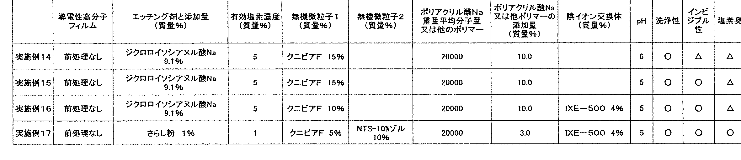
表3に示す割合で実施例1と同様にエッチングインクを調製して、スクリーン印刷を行った。
なお、実施例18、20、22および24では、実施例1と同じ導電フィルムを1%の硫酸水溶液に1時間浸漬させた後、水気をふき取ってから室温で12時間乾燥させた酸処理導電フィルムを用いた。
また、実施例19、21、23および25では、実施例1と同じ導電フィルムをゴーセノールNL-05(日本合成化学工業社製、ポリビニルアルコール)の10%水溶液を塗布した後、室温で12時間乾燥させた被膜付導電フィルムを用いた。

表4の結果から明らかなように、導電フィルムの酸処理および被膜付処理を行うことで、未印刷部分の抵抗上昇が抑制される。

洗浄性の評価基準
○:印刷30分後に洗浄してもインクが綺麗に洗い流せる。
×:印刷5分後に洗浄してもインクが固着してフィルム上に残る。
インビジブル性の評価基準
目視でエッチング部分と未エッチング部分を比べて、パターンの色が変化しているかを確認する。
○:目視でパターンがほとんど見えない。
△:目視でパターンが若干見える。
×:目視でパターンが見える。
塩素臭の評価基準
○:塩素臭が殆どない。
△:多少塩素臭があるが、通常の実験室雰囲気下での取り扱いが可能である。
×:塩素臭が強く、通常の実験室雰囲気下での取り扱いが不可である。
連続処理時の印刷精度の評価基準
×:5枚連続印刷するとパターンのかすれやにじみが生じる。
△:25枚連続印刷するとパターンのかすれやにじみが生じる。
○:50枚連続印刷してもパターン通りに印刷できる。
連続印刷処理可能枚数
インク印刷箇所の表面抵抗が109Ω/□以上に上昇し、かつ、インビジブル性を維持した枚数を示す。
揮発有効塩素による未印刷部分の抵抗上昇
印刷中にインクから揮発した有効塩素による、インク未印刷部の抵抗の上昇を比較する。
○:抵抗変化が20%未満である。
△:抵抗変化が20%~50%である。
×:抵抗変化が50%を超える。
なお、表4では評価区分である△に該当する評価はなかった。
・クニピアF(商品名):クニミネ工業社製、平板状ベントナイト
・ベンゲルHVP(商品名):ホージュン社製、平板状ベントナイト
・NTS-10%ゾル:トピー工業社製、平板状マイカ
・アロエジルCOK84(商品名):日本アロエジル社製、球状でシリカ:アルミナ=5:1の混合物
他のポリマーの略号は以下のとおりである。
・AA-MAA共重合体:アクリル酸とメタクリル酸の共重合体であり、実施例8では、アクリル酸/メタクリル酸=5/2(質量比)を使用している。
また、陰イオン交換体は以下のとおりである。
・IXE-500(商品名):東亜合成社製、ビスマス系陰イオン交換体
したがって、高分子有機ELディスプレイに代表されるディスプレイの表示画素部分の導電性高分子および周辺回路と導電性高分子の接続部分のパターニング、タッチパネルの検出部分の導電性高分子および周辺回路と導電性高分子の接続部分のパターニング、コンデンサー製造時に不要部分に付着した導電性高分子の除去などのエッチングが必要な用途において導電性高分子の利用が促進されることが期待される。
Claims (10)
- 導電性高分子用エッチング剤(A)、無機粒子(B)、ポリアクリル酸またはその塩(C)および水系媒体(D)を含み、pHが3~7に調整された導電性高分子用インビジブルエッチングインク。
- 導電性高分子用エッチング剤(A)が次亜塩素酸塩および/または次亜塩素酸塩5水和物である請求項1に記載の導電性高分子用インビジブルエッチングインク。
- 無機粒子(B)の一次粒子形状が平板状である請求項1または請求項2に記載の導電性高分子用インビジブルエッチングインク。
- 無機粒子がベントナイトおよび/またはマイカである請求項1~3のいずれかに記載の導電性高分子用インビジブルエッチングインク。
- ポリアクリル酸またはその塩の重量平均分子量が1000~50万である請求項1~4のいずれかに記載の導電性高分子用インビジブルエッチングインク。
- さらに、陰イオン交換体(E)を含む請求項1~5のいずれかに記載の導電性高分子用インビジブルエッチングインク。
- 陰イオン交換体(E)がビスマス系化合物またはハイドロタルサルトである請求項6に記載の導電性高分子用インビジブルエッチングインク。
- 基材上に導電性高分子の膜を形成する成膜工程、
前記膜における導電性高分子を除去する領域に請求項1~7のいずれか1つに記載の導電性高分子用インビジブルエッチングインクを付与する印刷工程、
前記導電性高分子用インビジブルエッチングインクにより前記除去する領域の導電性高分子をエッチングするエッチング工程、並びに、
残存する導電性高分子用インビジブルエッチングインクおよび導電性高分子のエッチング残液を基板上より除去する除去工程を含むことを特徴とする導電性高分子のパターニング方法。 - 前記導電性高分子が、ポリアニリン類、ポリピロール類またはポリチオフェン類である請求項8に記載の導電性高分子のパターニング方法。
- 印刷工程の前に、導電性高分子の膜を酸に浸漬させる、または導電性高分子の膜に水溶性樹脂の保護膜を形成させる工程を含む請求項8または請求項9に記載の導電性高分子のパターニング方法。
Priority Applications (3)
| Application Number | Priority Date | Filing Date | Title |
|---|---|---|---|
| KR1020177037611A KR20180084017A (ko) | 2015-11-20 | 2016-10-27 | 도전성 고분자용 인비저블 에칭 잉크 및 도전성 고분자의 패터닝 방법 |
| JP2017551796A JP6443563B2 (ja) | 2015-11-20 | 2016-10-27 | 導電性高分子用インビジブルエッチングインクおよび導電性高分子のパターニング方法 |
| CN201680041158.0A CN107849378A (zh) | 2015-11-20 | 2016-10-27 | 导电性高分子用隐形蚀刻墨液和导电性高分子的图案化方法 |
Applications Claiming Priority (2)
| Application Number | Priority Date | Filing Date | Title |
|---|---|---|---|
| JP2015-227464 | 2015-11-20 | ||
| JP2015227464 | 2015-11-20 |
Publications (1)
| Publication Number | Publication Date |
|---|---|
| WO2017086112A1 true WO2017086112A1 (ja) | 2017-05-26 |
Family
ID=58718734
Family Applications (1)
| Application Number | Title | Priority Date | Filing Date |
|---|---|---|---|
| PCT/JP2016/081798 Ceased WO2017086112A1 (ja) | 2015-11-20 | 2016-10-27 | 導電性高分子用インビジブルエッチングインクおよび導電性高分子のパターニング方法 |
Country Status (5)
| Country | Link |
|---|---|
| JP (1) | JP6443563B2 (ja) |
| KR (1) | KR20180084017A (ja) |
| CN (1) | CN107849378A (ja) |
| TW (1) | TW201730292A (ja) |
| WO (1) | WO2017086112A1 (ja) |
Cited By (2)
| Publication number | Priority date | Publication date | Assignee | Title |
|---|---|---|---|---|
| WO2022196049A1 (ja) * | 2021-03-19 | 2022-09-22 | 株式会社Screenホールディングス | 基板処理方法、および、基板処理装置 |
| WO2022196077A1 (ja) * | 2021-03-19 | 2022-09-22 | 株式会社Screenホールディングス | 基板処理方法、および、基板処理装置 |
Citations (5)
| Publication number | Priority date | Publication date | Assignee | Title |
|---|---|---|---|---|
| JP2001035276A (ja) * | 1999-05-20 | 2001-02-09 | Agfa Gevaert Nv | 導電性ポリマーの層のパターン化方法 |
| JP2007503697A (ja) * | 2003-08-26 | 2007-02-22 | イーストマン コダック カンパニー | 支持体上の導電性層のパターン形成 |
| WO2008041461A1 (en) * | 2006-09-29 | 2008-04-10 | Tsurumi Soda Co., Ltd. | Etching liquid for conductive polymer and method for patterning conductive polymer |
| JP2008088231A (ja) * | 2006-09-29 | 2008-04-17 | Tsurumi Soda Co Ltd | 導電性高分子用エッチング液および導電性高分子をパターニングする方法 |
| WO2011125603A1 (ja) * | 2010-04-09 | 2011-10-13 | 鶴見曹達株式会社 | 導電性高分子エッチング用インク及び導電性高分子のパターニング方法 |
Family Cites Families (4)
| Publication number | Priority date | Publication date | Assignee | Title |
|---|---|---|---|---|
| JP5724213B2 (ja) | 2010-05-13 | 2015-05-27 | セイコーエプソン株式会社 | 検出装置 |
| WO2013007362A1 (en) * | 2011-07-08 | 2013-01-17 | Heraeus Precious Metals Gmbh & Co. Kg | Process for the production of a layered body and layered bodies obtainable therefrom |
| US9017927B2 (en) * | 2013-02-25 | 2015-04-28 | Eastman Kodak Company | Patterning of transparent conductive coatings |
| WO2014150577A1 (en) * | 2013-03-15 | 2014-09-25 | Sinovia Technologies | Photoactive transparent conductive films, method of making them and touch sensitive device comprising said films |
-
2016
- 2016-10-14 TW TW105133263A patent/TW201730292A/zh unknown
- 2016-10-27 JP JP2017551796A patent/JP6443563B2/ja active Active
- 2016-10-27 CN CN201680041158.0A patent/CN107849378A/zh active Pending
- 2016-10-27 WO PCT/JP2016/081798 patent/WO2017086112A1/ja not_active Ceased
- 2016-10-27 KR KR1020177037611A patent/KR20180084017A/ko not_active Withdrawn
Patent Citations (5)
| Publication number | Priority date | Publication date | Assignee | Title |
|---|---|---|---|---|
| JP2001035276A (ja) * | 1999-05-20 | 2001-02-09 | Agfa Gevaert Nv | 導電性ポリマーの層のパターン化方法 |
| JP2007503697A (ja) * | 2003-08-26 | 2007-02-22 | イーストマン コダック カンパニー | 支持体上の導電性層のパターン形成 |
| WO2008041461A1 (en) * | 2006-09-29 | 2008-04-10 | Tsurumi Soda Co., Ltd. | Etching liquid for conductive polymer and method for patterning conductive polymer |
| JP2008088231A (ja) * | 2006-09-29 | 2008-04-17 | Tsurumi Soda Co Ltd | 導電性高分子用エッチング液および導電性高分子をパターニングする方法 |
| WO2011125603A1 (ja) * | 2010-04-09 | 2011-10-13 | 鶴見曹達株式会社 | 導電性高分子エッチング用インク及び導電性高分子のパターニング方法 |
Non-Patent Citations (1)
| Title |
|---|
| TAKASHI IHARA ET AL.: "Patterning Chemicals for conductive Polymer "CLEARIMAJU"", TOA GOSEI GROUP KENKYU NENPO, vol. 17, 2014, pages 15 - 19, XP055596216 * |
Cited By (7)
| Publication number | Priority date | Publication date | Assignee | Title |
|---|---|---|---|---|
| WO2022196049A1 (ja) * | 2021-03-19 | 2022-09-22 | 株式会社Screenホールディングス | 基板処理方法、および、基板処理装置 |
| WO2022196077A1 (ja) * | 2021-03-19 | 2022-09-22 | 株式会社Screenホールディングス | 基板処理方法、および、基板処理装置 |
| JP2022145165A (ja) * | 2021-03-19 | 2022-10-03 | 株式会社Screenホールディングス | 基板処理方法、および、基板処理装置 |
| JP2022145166A (ja) * | 2021-03-19 | 2022-10-03 | 株式会社Screenホールディングス | 基板処理方法、および、基板処理装置 |
| TWI813155B (zh) * | 2021-03-19 | 2023-08-21 | 日商斯庫林集團股份有限公司 | 基板處理方法以及基板處理裝置 |
| JP7606896B2 (ja) | 2021-03-19 | 2024-12-26 | 株式会社Screenホールディングス | 基板処理方法、および、基板処理装置 |
| JP7682656B2 (ja) | 2021-03-19 | 2025-05-26 | 株式会社Screenホールディングス | 基板処理方法、および、基板処理装置 |
Also Published As
| Publication number | Publication date |
|---|---|
| JP6443563B2 (ja) | 2018-12-26 |
| KR20180084017A (ko) | 2018-07-24 |
| CN107849378A (zh) | 2018-03-27 |
| JPWO2017086112A1 (ja) | 2018-05-24 |
| TW201730292A (zh) | 2017-09-01 |
Similar Documents
| Publication | Publication Date | Title |
|---|---|---|
| KR101872040B1 (ko) | 도전성 고분자 에칭용 잉크 및 도전성 고분자의 패터닝 방법 | |
| CN103456626B (zh) | 导电性高分子用蚀刻液、及将导电性高分子图案化的方法 | |
| KR20010020856A (ko) | 전도성 중합체 층을 패턴화하는 방법 | |
| KR20110086707A (ko) | 패터닝된 도전성 고분자막을 갖는 기판의 제조 방법 및 패터닝된 도전성 고분자막을 갖는 기판 | |
| JP6443563B2 (ja) | 導電性高分子用インビジブルエッチングインクおよび導電性高分子のパターニング方法 | |
| JP5080180B2 (ja) | 導電性高分子用エッチング液、及び、導電性高分子をパターニングする方法 | |
| JP5303994B2 (ja) | エッチング方法、及び、導電性高分子を有する基板 | |
| JP6477420B2 (ja) | 導電性高分子用エッチングインクおよび導電性高分子のパターニング方法 | |
| JP5943195B2 (ja) | 導電性高分子のエッチング液、およびエッチング液を用いた導電性高分子パターンの形成方法。 | |
| JP5688395B2 (ja) | 導電性パターンの形成方法、および透明導電性フィルム | |
| JP5020591B2 (ja) | 導電性高分子用エッチング液および導電性高分子をパターニングする方法 | |
| JP4881689B2 (ja) | 導電性高分子用エッチング液、及び、導電性高分子をパターニングする方法 | |
| JP2013120811A (ja) | 導電性樹脂パターンを有する積層体の製造方法および積層体 | |
| CN103772727B (zh) | 钝化组合物及其应用 | |
| JP2008115310A (ja) | 導電性高分子用エッチング液及び導電性高分子をパターニングする方法 | |
| KR101330064B1 (ko) | 전도성 고분자 막용 에칭 페이스트 조성물 및 이를 이용하여 전도성 고분자 막을 패터닝하는 방법 |
Legal Events
| Date | Code | Title | Description |
|---|---|---|---|
| 121 | Ep: the epo has been informed by wipo that ep was designated in this application |
Ref document number: 16866114 Country of ref document: EP Kind code of ref document: A1 |
|
| ENP | Entry into the national phase |
Ref document number: 2017551796 Country of ref document: JP Kind code of ref document: A |
|
| ENP | Entry into the national phase |
Ref document number: 20177037611 Country of ref document: KR Kind code of ref document: A |
|
| NENP | Non-entry into the national phase |
Ref country code: DE |
|
| 122 | Ep: pct application non-entry in european phase |
Ref document number: 16866114 Country of ref document: EP Kind code of ref document: A1 |