WO2017082029A1 - 多層基板、部品実装基板及び部品実装基板の製造方法 - Google Patents
多層基板、部品実装基板及び部品実装基板の製造方法 Download PDFInfo
- Publication number
- WO2017082029A1 WO2017082029A1 PCT/JP2016/081426 JP2016081426W WO2017082029A1 WO 2017082029 A1 WO2017082029 A1 WO 2017082029A1 JP 2016081426 W JP2016081426 W JP 2016081426W WO 2017082029 A1 WO2017082029 A1 WO 2017082029A1
- Authority
- WO
- WIPO (PCT)
- Prior art keywords
- external electrode
- dummy conductor
- dummy
- multilayer substrate
- conductor
- Prior art date
- Legal status (The legal status is an assumption and is not a legal conclusion. Google has not performed a legal analysis and makes no representation as to the accuracy of the status listed.)
- Ceased
Links
Images










Classifications
-
- H—ELECTRICITY
- H10—SEMICONDUCTOR DEVICES; ELECTRIC SOLID-STATE DEVICES NOT OTHERWISE PROVIDED FOR
- H10W—GENERIC PACKAGES, INTERCONNECTIONS, CONNECTORS OR OTHER CONSTRUCTIONAL DETAILS OF DEVICES COVERED BY CLASS H10
- H10W70/00—Package substrates; Interposers; Redistribution layers [RDL]
- H10W70/60—Insulating or insulated package substrates; Interposers; Redistribution layers
- H10W70/67—Insulating or insulated package substrates; Interposers; Redistribution layers characterised by their insulating layers or insulating parts
- H10W70/68—Shapes or dispositions thereof
- H10W70/685—Shapes or dispositions thereof comprising multiple insulating layers
-
- H—ELECTRICITY
- H05—ELECTRIC TECHNIQUES NOT OTHERWISE PROVIDED FOR
- H05K—PRINTED CIRCUITS; CASINGS OR CONSTRUCTIONAL DETAILS OF ELECTRIC APPARATUS; MANUFACTURE OF ASSEMBLAGES OF ELECTRICAL COMPONENTS
- H05K1/00—Printed circuits
- H05K1/02—Details
-
- H—ELECTRICITY
- H05—ELECTRIC TECHNIQUES NOT OTHERWISE PROVIDED FOR
- H05K—PRINTED CIRCUITS; CASINGS OR CONSTRUCTIONAL DETAILS OF ELECTRIC APPARATUS; MANUFACTURE OF ASSEMBLAGES OF ELECTRICAL COMPONENTS
- H05K1/00—Printed circuits
- H05K1/02—Details
- H05K1/0296—Conductive pattern lay-out details not covered by sub groups H05K1/02 - H05K1/0295
- H05K1/0298—Multilayer circuits
-
- H—ELECTRICITY
- H05—ELECTRIC TECHNIQUES NOT OTHERWISE PROVIDED FOR
- H05K—PRINTED CIRCUITS; CASINGS OR CONSTRUCTIONAL DETAILS OF ELECTRIC APPARATUS; MANUFACTURE OF ASSEMBLAGES OF ELECTRICAL COMPONENTS
- H05K3/00—Apparatus or processes for manufacturing printed circuits
- H05K3/30—Assembling printed circuits with electric components, e.g. with resistors
- H05K3/32—Assembling printed circuits with electric components, e.g. with resistors electrically connecting electric components or wires to printed circuits
-
- H—ELECTRICITY
- H05—ELECTRIC TECHNIQUES NOT OTHERWISE PROVIDED FOR
- H05K—PRINTED CIRCUITS; CASINGS OR CONSTRUCTIONAL DETAILS OF ELECTRIC APPARATUS; MANUFACTURE OF ASSEMBLAGES OF ELECTRICAL COMPONENTS
- H05K3/00—Apparatus or processes for manufacturing printed circuits
- H05K3/46—Manufacturing multilayer circuits
-
- H—ELECTRICITY
- H10—SEMICONDUCTOR DEVICES; ELECTRIC SOLID-STATE DEVICES NOT OTHERWISE PROVIDED FOR
- H10W—GENERIC PACKAGES, INTERCONNECTIONS, CONNECTORS OR OTHER CONSTRUCTIONAL DETAILS OF DEVICES COVERED BY CLASS H10
- H10W70/00—Package substrates; Interposers; Redistribution layers [RDL]
- H10W70/01—Manufacture or treatment
- H10W70/05—Manufacture or treatment of insulating or insulated package substrates, or of interposers, or of redistribution layers
-
- H—ELECTRICITY
- H10—SEMICONDUCTOR DEVICES; ELECTRIC SOLID-STATE DEVICES NOT OTHERWISE PROVIDED FOR
- H10W—GENERIC PACKAGES, INTERCONNECTIONS, CONNECTORS OR OTHER CONSTRUCTIONAL DETAILS OF DEVICES COVERED BY CLASS H10
- H10W70/00—Package substrates; Interposers; Redistribution layers [RDL]
- H10W70/01—Manufacture or treatment
- H10W70/05—Manufacture or treatment of insulating or insulated package substrates, or of interposers, or of redistribution layers
- H10W70/093—Connecting or disconnecting other interconnections thereto or therefrom, e.g. connecting bond wires or bumps
-
- H—ELECTRICITY
- H10—SEMICONDUCTOR DEVICES; ELECTRIC SOLID-STATE DEVICES NOT OTHERWISE PROVIDED FOR
- H10W—GENERIC PACKAGES, INTERCONNECTIONS, CONNECTORS OR OTHER CONSTRUCTIONAL DETAILS OF DEVICES COVERED BY CLASS H10
- H10W70/00—Package substrates; Interposers; Redistribution layers [RDL]
- H10W70/60—Insulating or insulated package substrates; Interposers; Redistribution layers
- H10W70/62—Insulating or insulated package substrates; Interposers; Redistribution layers characterised by their interconnections
- H10W70/63—Vias, e.g. via plugs
- H10W70/635—Through-vias
-
- H—ELECTRICITY
- H10—SEMICONDUCTOR DEVICES; ELECTRIC SOLID-STATE DEVICES NOT OTHERWISE PROVIDED FOR
- H10W—GENERIC PACKAGES, INTERCONNECTIONS, CONNECTORS OR OTHER CONSTRUCTIONAL DETAILS OF DEVICES COVERED BY CLASS H10
- H10W70/00—Package substrates; Interposers; Redistribution layers [RDL]
- H10W70/60—Insulating or insulated package substrates; Interposers; Redistribution layers
- H10W70/62—Insulating or insulated package substrates; Interposers; Redistribution layers characterised by their interconnections
- H10W70/65—Shapes or dispositions of interconnections
-
- H—ELECTRICITY
- H10—SEMICONDUCTOR DEVICES; ELECTRIC SOLID-STATE DEVICES NOT OTHERWISE PROVIDED FOR
- H10W—GENERIC PACKAGES, INTERCONNECTIONS, CONNECTORS OR OTHER CONSTRUCTIONAL DETAILS OF DEVICES COVERED BY CLASS H10
- H10W70/00—Package substrates; Interposers; Redistribution layers [RDL]
- H10W70/60—Insulating or insulated package substrates; Interposers; Redistribution layers
- H10W70/67—Insulating or insulated package substrates; Interposers; Redistribution layers characterised by their insulating layers or insulating parts
- H10W70/69—Insulating materials thereof
- H10W70/695—Organic materials
-
- H—ELECTRICITY
- H10—SEMICONDUCTOR DEVICES; ELECTRIC SOLID-STATE DEVICES NOT OTHERWISE PROVIDED FOR
- H10W—GENERIC PACKAGES, INTERCONNECTIONS, CONNECTORS OR OTHER CONSTRUCTIONAL DETAILS OF DEVICES COVERED BY CLASS H10
- H10W90/00—Package configurations
- H10W90/701—Package configurations characterised by the relative positions of pads or connectors relative to package parts
-
- H—ELECTRICITY
- H05—ELECTRIC TECHNIQUES NOT OTHERWISE PROVIDED FOR
- H05K—PRINTED CIRCUITS; CASINGS OR CONSTRUCTIONAL DETAILS OF ELECTRIC APPARATUS; MANUFACTURE OF ASSEMBLAGES OF ELECTRICAL COMPONENTS
- H05K2201/00—Indexing scheme relating to printed circuits covered by H05K1/00
- H05K2201/01—Dielectrics
- H05K2201/0137—Materials
- H05K2201/0141—Liquid crystal polymer [LCP]
-
- H—ELECTRICITY
- H05—ELECTRIC TECHNIQUES NOT OTHERWISE PROVIDED FOR
- H05K—PRINTED CIRCUITS; CASINGS OR CONSTRUCTIONAL DETAILS OF ELECTRIC APPARATUS; MANUFACTURE OF ASSEMBLAGES OF ELECTRICAL COMPONENTS
- H05K2201/00—Indexing scheme relating to printed circuits covered by H05K1/00
- H05K2201/01—Dielectrics
- H05K2201/0137—Materials
- H05K2201/0154—Polyimide
-
- H—ELECTRICITY
- H05—ELECTRIC TECHNIQUES NOT OTHERWISE PROVIDED FOR
- H05K—PRINTED CIRCUITS; CASINGS OR CONSTRUCTIONAL DETAILS OF ELECTRIC APPARATUS; MANUFACTURE OF ASSEMBLAGES OF ELECTRICAL COMPONENTS
- H05K2201/00—Indexing scheme relating to printed circuits covered by H05K1/00
- H05K2201/09—Shape and layout
- H05K2201/09209—Shape and layout details of conductors
- H05K2201/095—Conductive through-holes or vias
- H05K2201/09536—Buried plated through-holes, i.e. plated through-holes formed in a core before lamination
-
- H—ELECTRICITY
- H05—ELECTRIC TECHNIQUES NOT OTHERWISE PROVIDED FOR
- H05K—PRINTED CIRCUITS; CASINGS OR CONSTRUCTIONAL DETAILS OF ELECTRIC APPARATUS; MANUFACTURE OF ASSEMBLAGES OF ELECTRICAL COMPONENTS
- H05K2201/00—Indexing scheme relating to printed circuits covered by H05K1/00
- H05K2201/09—Shape and layout
- H05K2201/09209—Shape and layout details of conductors
- H05K2201/09654—Shape and layout details of conductors covering at least two types of conductors provided for in H05K2201/09218 - H05K2201/095
- H05K2201/09781—Dummy conductors, i.e. not used for normal transport of current; Dummy electrodes of components
-
- H—ELECTRICITY
- H05—ELECTRIC TECHNIQUES NOT OTHERWISE PROVIDED FOR
- H05K—PRINTED CIRCUITS; CASINGS OR CONSTRUCTIONAL DETAILS OF ELECTRIC APPARATUS; MANUFACTURE OF ASSEMBLAGES OF ELECTRICAL COMPONENTS
- H05K2201/00—Indexing scheme relating to printed circuits covered by H05K1/00
- H05K2201/10—Details of components or other objects attached to or integrated in a printed circuit board
- H05K2201/10613—Details of electrical connections of non-printed components, e.g. special leads
- H05K2201/10621—Components characterised by their electrical contacts
- H05K2201/10674—Flip chip
-
- H—ELECTRICITY
- H05—ELECTRIC TECHNIQUES NOT OTHERWISE PROVIDED FOR
- H05K—PRINTED CIRCUITS; CASINGS OR CONSTRUCTIONAL DETAILS OF ELECTRIC APPARATUS; MANUFACTURE OF ASSEMBLAGES OF ELECTRICAL COMPONENTS
- H05K2203/00—Indexing scheme relating to apparatus or processes for manufacturing printed circuits covered by H05K3/00
- H05K2203/02—Details related to mechanical or acoustic processing, e.g. drilling, punching, cutting, using ultrasound
- H05K2203/0285—Using ultrasound, e.g. for cleaning, soldering or wet treatment
-
- H—ELECTRICITY
- H05—ELECTRIC TECHNIQUES NOT OTHERWISE PROVIDED FOR
- H05K—PRINTED CIRCUITS; CASINGS OR CONSTRUCTIONAL DETAILS OF ELECTRIC APPARATUS; MANUFACTURE OF ASSEMBLAGES OF ELECTRICAL COMPONENTS
- H05K3/00—Apparatus or processes for manufacturing printed circuits
- H05K3/46—Manufacturing multilayer circuits
- H05K3/4611—Manufacturing multilayer circuits by laminating two or more circuit boards
- H05K3/4626—Manufacturing multilayer circuits by laminating two or more circuit boards characterised by the insulating layers or materials
- H05K3/4635—Manufacturing multilayer circuits by laminating two or more circuit boards characterised by the insulating layers or materials laminating flexible circuit boards using additional insulating adhesive materials between the boards
-
- H—ELECTRICITY
- H10—SEMICONDUCTOR DEVICES; ELECTRIC SOLID-STATE DEVICES NOT OTHERWISE PROVIDED FOR
- H10W—GENERIC PACKAGES, INTERCONNECTIONS, CONNECTORS OR OTHER CONSTRUCTIONAL DETAILS OF DEVICES COVERED BY CLASS H10
- H10W72/00—Interconnections or connectors in packages
- H10W72/071—Connecting or disconnecting
- H10W72/072—Connecting or disconnecting of bump connectors
-
- H—ELECTRICITY
- H10—SEMICONDUCTOR DEVICES; ELECTRIC SOLID-STATE DEVICES NOT OTHERWISE PROVIDED FOR
- H10W—GENERIC PACKAGES, INTERCONNECTIONS, CONNECTORS OR OTHER CONSTRUCTIONAL DETAILS OF DEVICES COVERED BY CLASS H10
- H10W72/00—Interconnections or connectors in packages
- H10W72/071—Connecting or disconnecting
- H10W72/072—Connecting or disconnecting of bump connectors
- H10W72/07231—Techniques
- H10W72/07232—Compression bonding, e.g. thermocompression bonding
- H10W72/07233—Ultrasonic bonding, e.g. thermosonic bonding
-
- H—ELECTRICITY
- H10—SEMICONDUCTOR DEVICES; ELECTRIC SOLID-STATE DEVICES NOT OTHERWISE PROVIDED FOR
- H10W—GENERIC PACKAGES, INTERCONNECTIONS, CONNECTORS OR OTHER CONSTRUCTIONAL DETAILS OF DEVICES COVERED BY CLASS H10
- H10W72/00—Interconnections or connectors in packages
- H10W72/071—Connecting or disconnecting
- H10W72/072—Connecting or disconnecting of bump connectors
- H10W72/07251—Connecting or disconnecting of bump connectors characterised by changes in properties of the bump connectors during connecting
- H10W72/07254—Connecting or disconnecting of bump connectors characterised by changes in properties of the bump connectors during connecting changes in dispositions
-
- H—ELECTRICITY
- H10—SEMICONDUCTOR DEVICES; ELECTRIC SOLID-STATE DEVICES NOT OTHERWISE PROVIDED FOR
- H10W—GENERIC PACKAGES, INTERCONNECTIONS, CONNECTORS OR OTHER CONSTRUCTIONAL DETAILS OF DEVICES COVERED BY CLASS H10
- H10W72/00—Interconnections or connectors in packages
- H10W72/20—Bump connectors, e.g. solder bumps or copper pillars; Dummy bumps; Thermal bumps
- H10W72/241—Dispositions, e.g. layouts
-
- H—ELECTRICITY
- H10—SEMICONDUCTOR DEVICES; ELECTRIC SOLID-STATE DEVICES NOT OTHERWISE PROVIDED FOR
- H10W—GENERIC PACKAGES, INTERCONNECTIONS, CONNECTORS OR OTHER CONSTRUCTIONAL DETAILS OF DEVICES COVERED BY CLASS H10
- H10W72/00—Interconnections or connectors in packages
- H10W72/20—Bump connectors, e.g. solder bumps or copper pillars; Dummy bumps; Thermal bumps
- H10W72/241—Dispositions, e.g. layouts
- H10W72/244—Dispositions, e.g. layouts relative to underlying supporting features, e.g. bond pads, RDLs or vias
-
- H—ELECTRICITY
- H10—SEMICONDUCTOR DEVICES; ELECTRIC SOLID-STATE DEVICES NOT OTHERWISE PROVIDED FOR
- H10W—GENERIC PACKAGES, INTERCONNECTIONS, CONNECTORS OR OTHER CONSTRUCTIONAL DETAILS OF DEVICES COVERED BY CLASS H10
- H10W72/00—Interconnections or connectors in packages
- H10W72/20—Bump connectors, e.g. solder bumps or copper pillars; Dummy bumps; Thermal bumps
- H10W72/241—Dispositions, e.g. layouts
- H10W72/247—Dispositions of multiple bumps
-
- H—ELECTRICITY
- H10—SEMICONDUCTOR DEVICES; ELECTRIC SOLID-STATE DEVICES NOT OTHERWISE PROVIDED FOR
- H10W—GENERIC PACKAGES, INTERCONNECTIONS, CONNECTORS OR OTHER CONSTRUCTIONAL DETAILS OF DEVICES COVERED BY CLASS H10
- H10W72/00—Interconnections or connectors in packages
- H10W72/20—Bump connectors, e.g. solder bumps or copper pillars; Dummy bumps; Thermal bumps
- H10W72/251—Materials
- H10W72/252—Materials comprising solid metals or solid metalloids, e.g. PbSn, Ag or Cu
-
- H—ELECTRICITY
- H10—SEMICONDUCTOR DEVICES; ELECTRIC SOLID-STATE DEVICES NOT OTHERWISE PROVIDED FOR
- H10W—GENERIC PACKAGES, INTERCONNECTIONS, CONNECTORS OR OTHER CONSTRUCTIONAL DETAILS OF DEVICES COVERED BY CLASS H10
- H10W90/00—Package configurations
- H10W90/701—Package configurations characterised by the relative positions of pads or connectors relative to package parts
- H10W90/721—Package configurations characterised by the relative positions of pads or connectors relative to package parts of bump connectors
- H10W90/724—Package configurations characterised by the relative positions of pads or connectors relative to package parts of bump connectors between a chip and a stacked insulating package substrate, interposer or RDL
Definitions
- the present invention relates to a multilayer board made of a thermoplastic resin, a component mounting board, and a method for manufacturing the component mounting board.
- the semiconductor mounting method is a method of mounting bumps of a semiconductor bare chip on the wiring of a flexible wiring board using a liquid crystal polymer film by an ultrasonic flip chip bonding technique. By applying ultrasonic vibration to the semiconductor chip in substantially the same direction of the liquid crystal polymer, the wiring and the bump are joined.
- the semiconductor bare chip may have a dense region where bumps are densely present and a sparse region where bumps are sparsely present.
- the flexible wiring board has a dense region where the wiring to which the bumps of the semiconductor bare chip are bonded is dense and a sparse region where the wiring is sparse. Therefore, at the time of mounting, relatively many bumps and wirings are in contact with each other in the dense area, and relatively few bumps and wirings are in contact with each other in the sparse area.
- the semiconductor bare chip when applying ultrasonic vibration to the semiconductor bare chip, the semiconductor bare chip is pressed against the flexible wiring board by pressing the upper surface of the semiconductor bare chip with a mounting machine. Therefore, force is applied from the semiconductor bare chip to the flexible wiring board. Since a relatively large number of bumps and wirings are in contact with each other in the dense region and a relatively small number of bumps and wirings are in contact with each other in the sparse region, the force applied to the dense region is larger than the force applied to the sparse region. As a result, the wiring in the dense region sinks more than the wiring in the sparse region, and the semiconductor bare chip is tilted.
- an object of the present invention is to provide a multilayer substrate, a component mounting substrate, and a method for manufacturing the component mounting substrate that can suppress the mounting component from being inclined on the multilayer substrate.
- a multilayer substrate has a principal surface and a flexible element body, a first external electrode or a first external electrode provided on the principal surface and used for mounting a mounting component.
- the external electrode closest to the mth external electrode from the first external electrode to the nth external electrode from the mth external electrode (m is an integer of 1 to n)
- a distance Dm is defined as a distance Dm
- an average of the distances D1 to Dn is defined as an average Dave, and when viewed from the normal direction, a circular shape having a center at the mth external electrode and a distance Dm as a radius.
- a region is defined as a region Am, and the first dummy conductor is in the normal direction. When viewed al, that are provided within at least a portion of the area Am of the one or more regions Am to the small distance Dm radius than the average Dave, characterized.
- a component mounting board includes the multilayer board and first to nth (n is an integer of 3 or more) bumps, and is mounted on the main surface.
- the mounting component wherein the first external electrode to the nth external electrode are ultrasonically bonded to the first bump to the nth bump, respectively. .
- a method for manufacturing a component mounting board includes a flexible body having a main surface and a first external electrode or nth (nth) n provided on the main surface. Is an integer of 3 or more) and at least one or more first dummy conductors provided in the element body and in a floating state, when viewed from the normal direction of the main surface And the distance from the m-th external electrode (m is an integer of 1 to n) to the external electrode closest to the m-th external electrode among the first external electrode to the n-th external electrode.
- a distance Dm is defined, an average of the distances D1 to Dn is defined as an average Dave, and when viewed from the normal direction, a circular area centered on the mth external electrode and having a radius of the distance Dm is defined as the area Am.
- a multilayer substrate provided in at least a part of the region Am having a radius Dm smaller than the average Dave, and a first bump to an nth (n is an integer of 3 or more)
- a component mounting board comprising: a mounting part having a bump; and forming the multilayer board including the first external electrode to the nth external electrode and the first dummy conductor. And a step of ultrasonically welding each of the first external electrode to the nth external electrode to the first bump to the nth bump.
- the present invention it is possible to suppress the mounting component from being inclined on the multilayer substrate.
- FIG. 1 is an external perspective view of a component mounting board 10 according to an embodiment of the present invention.
- FIG. 2 is an external perspective view of the mounting component 14.
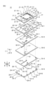
- FIG. 3 is an exploded perspective view of the multilayer substrate 12.
- FIG. 4 is a view of the insulator sheet 16-1 as viewed from above.
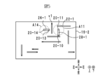
- FIG. 5 is a view of the insulator sheet 16-2 as viewed from above.
- FIG. 6 is a sectional structural view taken along the line AA in FIG.
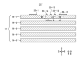
- FIG. 7 is a cross-sectional structure diagram of the component mounting board 10 at the time of manufacturing.
- FIG. 8 is a cross-sectional structure diagram of the component mounting board 10 at the time of manufacturing.
- FIG. 9 is a cross-sectional structure diagram of the component mounting board 10 at the time of manufacturing.
- FIG. 1 is an external perspective view of a component mounting board 10 according to an embodiment of the present invention.
- FIG. 2 is an external perspective view of the mounting component 14.
- FIG. 3 is an exploded perspective view of
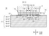
- FIG. 10 is a cross-sectional structure diagram of the component mounting board 10 at the time of manufacturing.
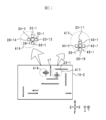
- FIG. 11 is a view of the insulator sheet 16-2 of the multilayer substrate 12a according to the first modification as viewed from above.
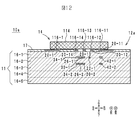
- FIG. 12 is a sectional structural view of a component mounting board 10a according to the first modification.
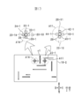
- FIG. 13 is a view of the insulator sheet 16-2 of the multilayer substrate 12b according to the second modification as viewed from above.
- FIG. 14 is a sectional structural view of a component mounting board 10b according to a second modification.
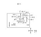
- FIG. 15 is a view of the insulator sheet 16-2 of the multilayer substrate 12c according to the third modification as viewed from above.
- FIG. 11 is a view of the insulator sheet 16-2 of the multilayer substrate 12a according to the first modification as viewed from above.
- FIG. 12 is a sectional structural view of a component mounting board 10a according to the first modification.
- FIG. 13 is a view of the
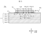
- FIG. 16 is a sectional structural view of a component mounting board 10c according to a third modification.
- FIG. 17 is a sectional structural view of a component mounting board 10d according to a fourth modification.
- FIG. 18 is a cross-sectional structure diagram of a component mounting board 10e according to a fifth modification.
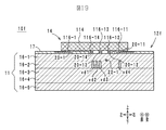
- FIG. 19 is a cross-sectional structure diagram of a component mounting board 10f according to a sixth modification.
- FIG. 20 is a cross-sectional structure diagram of a component mounting board 10g according to a seventh modification.
- FIG. 1 is an external perspective view of a component mounting board 10 according to an embodiment of the present invention.
- FIG. 2 is an external perspective view of the mounting component 14.
- FIG. 3 is an exploded perspective view of the multilayer substrate 12.
- FIG. 4 is a view of the insulator sheet 16-1 as viewed from above.
- FIG. 5 is a view of the insulator sheet 16-2 as viewed from above.
- FIG. 6 is a sectional structural view taken along the line AA in FIG.
- the stacking direction of the multilayer substrate 12 is defined as the vertical direction (an example of the normal direction of the main surface of the element body). Further, the longitudinal direction when the multilayer substrate 12 is viewed from the upper side is defined as the left-right direction, and the short direction when the multilayer substrate 12 is viewed from the upper side is defined as the front-rear direction.
- the up-down direction, the left-right direction, and the front-rear direction are orthogonal to each other.
- the component mounting board 10 is a module including a semiconductor integrated circuit provided in an electronic device such as a mobile phone. As shown in FIG. 1, the component mounting board 10 includes a multilayer board 12 and a mounting part 14.
- the mounting component 14 is, for example, a semiconductor integrated circuit such as an image sensor such as an RFIC or a CCD, and includes a main body 114 and bumps 116-1 to 116-14 as shown in FIG.
- the main body 114 has a rectangular plate shape when viewed from above.
- the upper main surface of the main body 114 is referred to as a front surface
- the lower main surface of the main body 114 is referred to as a back surface.
- Bumps 116-1 to 116-14 are provided on the back surface of the main body 114 and are external terminals used for connection to the multilayer substrate 12.
- the bumps 116-1 to 116-14 are made of, for example, a metal such as gold, and are spherical or hemispherical before mounting.
- the bumps 116-1 to 116-14 are arranged along the outer edge of the back surface of the main body 114. Specifically, the bumps 116-1 to 116-4 are arranged in this order from the rear side to the front side along the left side of the back surface of the main body 114.
- the bumps 116-4 to 116-7 are arranged in this order from the left side to the right side along the front side of the back surface of the main body 114.
- the bumps 116-7 to 116-11 are arranged in this order from the front side to the rear side along the right side of the back surface of the main body 114.
- the bumps 116-11 to 116-14 are arranged in this order from the right side to the left side along the rear side of the back surface of the main body 114.
- the intervals between the bumps 116-1 to 116-14 in the left-right direction and the front-rear direction are not uniform. As a result, there are areas where the bumps 116-1 to 116-14 are densely arranged and areas where the bumps 116-1 to 116-14 are sparsely arranged.
- the multilayer substrate 12 is a flexible substrate on which the mounting component 14 is mounted. As shown in FIG. 3, the multilayer substrate 12 includes an element body 11, a protective layer 17, external electrodes 20-1 to 20-14, 24-1 to 24-14, wiring conductor layers 22-1 to 22-3, dummy Conductor layers 26-1, 28-1 and via-hole conductors v1-v4 are provided.
- the wiring conductor layers are provided in addition to the wiring conductor layers 22-1 to 22-3, but the wiring conductor layers other than the wiring conductor layers 22-1 to 22-3 are omitted in FIG.
- the via hole conductors are provided in addition to the via hole conductors v1 to v4, but the via hole conductors other than the via hole conductors v1 to v4 are omitted in FIG. Further, in FIG. 3, only the representative wiring conductor layers and via-hole conductors are provided with reference numerals.
- the element body 11 is a flexible plate-like member that forms a rectangle when viewed from above.
- the long side of the element body 11 is parallel to the left-right direction.
- the element body 11 is a laminated body in which insulator sheets 16-1 to 16-5 (an example of a plurality of insulator layers) are laminated in this order from the upper side to the lower side. is there.
- the upper main surface of the element body 11 is referred to as a front surface
- the lower main surface of the element body 11 is referred to as a back surface.
- the insulator sheets 16-1 to 16-5 have a rectangular shape when viewed from above, and have the same shape as the element body 11.
- the long sides of the insulator sheets 16-1 to 16-5 are parallel to the left-right direction.
- the insulator sheets 16-1 to 16-5 are insulator layers made of a flexible thermoplastic resin such as polyimide or liquid crystal polymer.
- the upper main surface of the insulator sheets 16-1 to 16-5 is referred to as a front surface
- the lower main surface of the insulator sheets 16-1 to 16-5 is referred to as a back surface.
- the external electrodes 20-1 to 20-14 are rectangular conductor layers, and bumps 116-1 to 116 are formed on the surface of the insulator sheet 16-1. It is provided to correspond to -14. Hereinafter, the arrangement of the external electrodes 20-1 to 20-14 will be described in more detail.
- an area overlapping with the mounting component 14 when viewed from above is referred to as an area A0.
- the external electrodes 20-1 to 20-14 are arranged along the outer edge of the region A0 in the region A0. Specifically, the external electrodes 20-1 to 20-4 are arranged in this order from the rear side to the front side along the left side of the region A0.
- the external electrodes 20-4 to 20-7 are arranged in this order from the left side to the right side along the front side of the region A0.
- the external electrodes 20-7 to 20-11 are arranged in this order from the front side to the rear side along the right side of the region A0.
- the external electrodes 20-11 to 20-14 are arranged in this order from the right side to the left side along the rear side of the region A0.
- the distances D1 to D14 are defined as follows (see FIG. 4).
- Distance D1 When viewed from above, from the external electrode 20-1 to the external electrode (external electrode 20-2) closest to the external electrode 20-1 among the external electrodes 20-1 to 20-14 Distance (2) Distance D2: From the external electrode 20-2 to the external electrode closest to the external electrode 20-2 among the external electrodes 20-1 to 20-14 (external electrode 20-3) when viewed from above (3) Distance D3: External electrode closest to the external electrode 20-3 among the external electrodes 20-1 to 20-14 when viewed from above (external electrode 20-4) (4) Distance D4: When viewed from above, the external electrode closest to the external electrode 20-4 among the external electrodes 20-1 to 20-14 from the external electrode 20-4 (external electrode 20-3) (5) Distance D5: When viewed from above, the external electrode 20- Distance from the external electrode 20-1 to 20-14 to the external electrode (external electrode 20-4) closest to the external electrode 20-5 (6) Distance D6: When viewed from above, the external electrode 20- 6 to the external electrode (external electrode 20-7) closest to the external electrode
- the average of the distances D1 to D14 is defined as the average Dave.
- the following equation (1) is established between the distances D1 to D14 and the average Dave.
- the external electrodes 20-1 to 20-14 arranged as described above are used for mounting the mounting component 14. Specifically, the external electrodes 20-1 to 20-14 are bonded to the bumps 116-1 to 116-14 by ultrasonic welding (also referred to as ultrasonic bonding). During ultrasonic welding, the lower ends of the bumps 116-1 to 116-14 are slightly crushed as shown in FIG. That is, the bumps 116-1 to 116-14 are not in contact with the external electrodes 20-1 to 20-14 at points, but are in contact with the external electrodes 20-1 to 20-14 at the surface.
- ultrasonic welding also referred to as ultrasonic bonding
- the protective layer 17 is a resin layer that covers substantially the entire surface of the insulator sheet 16-1. However, the protective layer 17 is provided with rectangular openings 21-1 to 21-14 as shown in FIG. The openings 21-1 to 21-14 are portions where the protective layer 17 is not provided. The external electrodes 20-1 to 20-14 are exposed to the outside of the multilayer substrate 12 through the openings 21-1 to 21-14, respectively.
- the external electrodes 24-1 to 24-14 have a rectangular shape when viewed from above, and are used for mounting on a circuit board (not shown) such as a printed wiring board and the external electrodes 24-1 to 24-14. At least a portion of 24-14 is electrically connected to the circuit board.
- the external electrodes 24-1 to 24-14 are arranged along the outer edge of the back surface of the insulating sheet 16-5. Specifically, the external electrodes 24-1 to 24-4 are arranged in this order from the rear side to the front side along the left side of the back surface of the insulator sheet 16-5.
- the external electrodes 24-4 to 24-8 are arranged in this order from the left side to the right side along the front side of the back surface of the insulator sheet 16-5.
- the external electrodes 24-8 to 24-10 are arranged in this order from the front side to the rear side along the right side of the back surface of the insulating sheet 16-5.
- the external electrodes 24-10 to 24-14 are arranged in this order from the right side to the left side along the rear side of the back surface of the insulating sheet 16-5.
- the wiring conductor layers 22-1 to 22-3 are linear planar conductors provided on the surfaces of the insulator sheets 16-2 to 16-4, respectively. That is, the wiring conductor layers 22-1 to 22-3 are provided in the element body 11.
- the via-hole conductors v1 to v4 penetrate the insulator sheets 16-2 to 16-5 in the vertical direction, respectively.
- the via-hole conductor v1 connects the wiring conductor layer 22-1 and the wiring conductor layer 22-2.
- the via-hole conductor v2 connects the wiring conductor layer 22-2 and the wiring conductor layer 22-3.
- the via-hole conductors v3 and v4 connect the wiring conductor layer 22-3 and the external electrodes 24-1 to 24-14.
- the insulator sheet 16-1 is also provided with a via-hole conductor and a wiring conductor layer, which are omitted in FIG. Via the wiring conductor layers 22-1 to 22-3, the via-hole conductors v1 to v4, the wiring conductor layer (not shown), and the via-hole conductor (not shown), the external electrodes 20-1 to 20-14 and the external electrode 24-1 To 24-14 are electrically connected.
- the multilayer substrate 12 includes dummy conductor layers 26-1 and 28-1 (an example of a first dummy conductor and a first planar conductor). .
- the dummy conductor layers 26-1 and 28-1 will be described in more detail.
- the distances D1 to D14 are centered on the respective gravity centers of the external electrodes 20-1 to 20-14 (an example of the mth external electrode).
- regions A1 to A14 are defined as regions A1 to A14 (an example of the region Am) (only the regions A11 and A14 are shown in FIG. 5).
- Each of the dummy conductor layers 26-1 and 28-1 is a rectangular planar conductor provided on the surface of the insulating sheet 16-2 (that is, in the element body 11), and is connected to other conductors. It is in a floating state due to the absence.
- the floating state means a state where the conductor is not connected to a power supply potential or the like.
- the dummy conductor layers 26-1 and 28-1 are provided in the regions A14 and A11, respectively, when viewed from above.
- the dummy conductor layer 26-1 has a strip shape extending in the left-right direction, and overlaps the external electrodes 20-13 and 20-14 when viewed from above.
- the dummy conductor layer 28-1 has a strip shape extending in the front-rear direction, and overlaps the external electrodes 20-10 and 20-11 when viewed from above.
- the areas A14 and A11 are at least a part of the areas A3 to A5 and A8 to A14 whose radii are distances D3 to D5 and D8 to D14 smaller than the average Dave.
- the regions A3 to A5, A8 to A14 are external electrodes. Is a densely arranged region. Therefore, dummy conductor layers 26-1 and 28-1 are arranged in at least some of the regions A14 and A11 in the regions A3 to A5 and A8 to A14 where the external electrodes are densely arranged.
- the region A14 where the dummy conductor layer 26-1 is provided is a region having a radius of the smallest distance D14.
- the region A11 where the dummy conductor layer 28-1 is provided is a region having a radius of the sixth smallest distance D11.
- FIG. 7 to 10 are cross-sectional structure diagrams of the component mounting board 10 at the time of manufacturing.
- a case where one multilayer substrate 12 is manufactured will be described as an example, but actually, a plurality of multilayer substrates 12 are manufactured simultaneously by laminating and cutting large-sized insulator sheets.
- insulator sheets 16-1 to 16-5 made of a liquid crystal polymer are prepared.
- a copper foil is formed on the entire main surface of one of the insulator sheets 16-1 to 16-5.
- copper foil is attached to the surfaces of the insulating sheets 16-1 to 16-4.
- a copper foil is pasted on the back surface of the insulating sheet 16-5.
- the surface of the copper foil of the insulating sheets 16-1 to 16-5 is smoothed by applying, for example, zinc plating for rust prevention.
- metal foils other than copper foil may be used.
- the external electrodes 20-1 to 20-14 and a wiring conductor layer are formed on the insulator sheet as shown in FIG. Formed on the surface of 16-1.
- a resist having the same shape as the external electrodes 20-1 to 20-14 shown in FIG. 3 and a wiring conductor layer (not shown) is printed on the copper foil on the surface of the insulating sheet 16-1.
- the copper foil of the part which is not covered with the resist is removed by performing an etching process with respect to copper foil. Thereafter, the resist is removed by spraying a cleaning liquid (resist removing liquid).
- a cleaning liquid resist removing liquid
- wiring conductor layers 22-1 to 22-3 and dummy conductor layers 26-1 and 28-1 are formed on the surfaces of the insulating sheets 16-2 to 16-4, respectively. Further, as shown in FIG. 3, external electrodes 24-1 to 24-14 are formed on the back surface of the insulating sheet 16-5.
- the formation process of the wiring conductor layers 22-1 to 22-3, the external electrodes 24-1 to 24-14, and the dummy conductor layers 26-1 and 28-1 is not shown in the drawings. Since it is the same as the formation process of a wiring conductor layer, description is abbreviate
- through holes are formed by irradiating laser beams to positions where via-hole conductors v1 to v4 and via-hole conductors (not shown) of the insulating sheets 16-1 to 16-5 are formed. Then, the through hole is filled with a conductive paste mainly composed of a metal such as copper or silver.
- the multilayer substrate 12 is formed by thermocompression bonding. Specifically, as shown in FIG. 7, after the insulating sheets 16-1 to 16-5 are stacked, the insulating sheets 16-1 to 16-5 are subjected to pressure treatment and heat treatment (ie, heat treatment). Apply crimping. The pressurizing process is performed by sandwiching the insulator sheets 16-1 to 16-5 from above and below. By applying pressure treatment and heat treatment to the insulating sheets 16-1 to 16-5, the insulating sheets 16-1 to 16-5 are softened and the conductive paste in the through holes is solidified. As a result, the insulator sheets 16-1 to 16-5 are joined and the via-hole conductors v1 to v4 are formed. Through the above steps, the element body 11 is formed as shown in FIG.
- a protective layer 17 is formed on the surface of the insulator sheet 16-1 by applying a resin (resist) paste by screen printing.
- the multilayer substrate 12 is completed through the above steps.
- the mounting component 14 is mounted on the multilayer substrate 12. Specifically, the mounting component 14 is arranged on the multilayer substrate 12 so that the external electrodes 20-1 to 20-14 and the bumps 116-1 to 116-14 are in contact with each other. Thereafter, the ultrasonic bonding machine T is pressed against the upper surface of the mounting component 14 to operate the ultrasonic bonding machine T. As a result, the ultrasonic vibration is transmitted to the bumps 116-1 to 116-14 and the external electrodes 20-1 to 20-14 via the main body 114. The external electrodes 20-1 to 20-14 and the bumps 116-1 to 116-14 are metallurgically bonded by ultrasonic vibration. Through the above steps, the component mounting board 10 is completed.
- the mounting component 14 can be prevented from being inclined on the multilayer substrate 12.
- a multilayer substrate according to a comparative example of the multilayer substrate 12 a multilayer substrate that does not include the dummy conductor layers 26-1 and 28-1 will be described as an example.
- the reference numerals of the components of the multilayer board according to the comparative example the reference numerals of the multilayer board 12 are used.
- regions A3 to A5 and A8 to A14 are regions having a radius D3 to D5 and D8 to D14 smaller than the average Dave. Since the external electrodes exist near the external electrodes 20-3 to 20-5 and 20-8 to 20-14 corresponding to the regions A3 to A5, A8 to A14, the regions A3 to A5, A8 to A14 Is a region where external electrodes are densely arranged. On the other hand, regions A1, A2, A6, and A7 are regions where external electrodes are sparsely arranged.
- the force applied to the regions A3 to A5, A8 to A14 is larger than the force applied to the regions A1, A2, A6, and A7 during ultrasonic bonding.
- the regions A3 to A5, A8 to A14 sink more than the regions A1, A2, A6, and A7, and the mounting component 14 tilts.
- the dummy conductor layers 26-1 and 28-1 are provided in a part of the regions A14 and A11 in the regions A3 to A5 and A8 to A14 when viewed from above. .
- the dummy conductor layers 26-1 and 28-1 are less likely to be deformed than the insulator sheets 16-1 to 16-5. Therefore, the dummy conductor layers 26-1 and 28-1 prevent the areas A14 and A11 from sinking.
- the mounting component 14 can be prevented from being inclined on the multilayer substrate 12. When the mounting component 14 is prevented from being tilted, problems such as damage to the mounting component 14 are suppressed.
- the region A14 is a region having the smallest distance D14 as a radius. Therefore, when the mounting component 14 is mounted, the amount that the area A14 sinks is the largest of the amounts that the areas A1 to A14 sink. However, the amounts of sinking of the regions A3, A4, A12, A13, A14 are substantially equal to each other. Therefore, in the multilayer substrate 12, the dummy conductor layer 26-1 is provided in the region A14 when viewed from above. As a result, the number of areas where the sinking is large is reduced, and the mounting component 14 is more effectively suppressed from being inclined on the multilayer substrate 12. Most preferably, dummy conductor layers are provided in all of the regions A3, A4, A12, A13, and A14 where the sinking is large.
- the dummy conductor layers 26-1 and 28-1 are insulated from the insulating sheet 16-1 provided with the external electrodes 20-1 to 20-14.
- the body sheet 16-2 is provided. Therefore, short circuit between dummy conductor layers 26-1 and 28-1 and external electrodes 20-1 to 20-14 is suppressed.
- FIG. 11 is a view of the insulator sheet 16-2 of the multilayer substrate 12a according to the first modification as viewed from above.
- FIG. 12 is a sectional structural view of a component mounting board 10a according to the first modification.
- the multilayer substrate 12a is different from the multilayer substrate 12 in the following two points.
- the first difference is the shape and position of the dummy conductor layers 26-1 and 28-1.
- the second difference is that the dummy conductor layers 26-2, 28-2, 30-1, 32-1, 34-1, 36-1, 30-2, 32-2, 34-2, 36-2, 40-1, 42-1, 44-1, 46-1, 40-2, 42-2, 44-2, 46-2 (an example of a second dummy conductor) (dummy conductor layers 30-2, 34- 2, 40-2, 42-2, 44-2, and 46-2 are the presence or absence of not shown in FIGS.
- the multilayer substrate 12a and the component mounting substrate 10a will be described focusing on the first difference and the second difference.
- the dummy conductor layers 26-1 and 28-1 have a rectangular shape when viewed from above.
- the dummy conductor layer 26-1 is located between the external electrode 20-13 and the external electrode 20-14 when viewed from above, and does not overlap the external electrodes 20-13 and 20-14. .
- the dummy conductor layers 26-2 and 28-2 are different from the insulator sheet 16-2 on which the dummy conductor layers 26-1 and 28-1 are provided (that is, the surface of the insulator sheet 16-3). 11), and is in a floating state because it is not connected to other conductors.
- the dummy conductor layer 26-2 has the same shape as the dummy conductor layer 26-1, and overlaps with the dummy conductor layer 26-1 when viewed from above.
- the dummy conductor layer 28-2 has the same shape as the dummy conductor layer 28-1, and overlaps with the dummy conductor layer 28-1 when viewed from above.
- the dummy conductor layers 30-1, 32-1, 34-1 and 36-1 are respectively provided on the surface of the insulating sheet 16-2 on which the dummy conductor layer 26-1 is provided. It is arranged so as to surround the periphery of -1. That is, the dummy conductor layers 30-1, 32-1, 34-1 and 36-1 do not overlap the dummy conductor layer 26-1 when viewed from above. Specifically, the dummy conductor layer 30-1 is disposed on the right side with respect to the dummy conductor layer 26-1. The dummy conductor layer 32-1 is disposed behind the dummy conductor layer 26-1. The dummy conductor layer 34-1 is disposed on the left side with respect to the dummy conductor layer 26-1. The dummy conductor layer 36-1 is disposed in front of the dummy conductor layer 26-1. However, the centers of the dummy conductor layers 30-1, 32-1, 34-1 and 36-1 are arranged in the region A14 when viewed from above.
- the dummy conductor layers 30-2, 32-2, 34-2, and 36-2 are respectively provided on the surface of the insulator sheet 16-3 on which the dummy conductor layer 26-2 is provided. -2 is arranged so as to surround the periphery. That is, the dummy conductor layers 30-2, 32-2, 34-2, and 36-2 do not overlap the dummy conductor layers 26-1 and 26-2. Specifically, the dummy conductor layer 30-2 is disposed on the right side with respect to the dummy conductor layer 26-2. The dummy conductor layer 32-2 is disposed behind the dummy conductor layer 26-2. The dummy conductor layer 34-2 is disposed on the left side with respect to the dummy conductor layer 26-2. The dummy conductor layer 36-2 is disposed in front of the dummy conductor layer 26-2. However, the centers of the dummy conductor layers 30-2, 32-2, 34-2, and 36-2 are disposed in the region A14 when viewed from above.
- the dummy conductor layers 40-1, 42-1, 44-1 and 46-1 are respectively provided on the surface of the insulator sheet 16-2 on which the dummy conductor layer 28-1 is provided. It is arranged so as to surround the periphery of -1. That is, the dummy conductor layers 40-1, 42-1, 44-1 and 46-1 do not overlap the dummy conductor layer 28-1. Specifically, the dummy conductor layer 40-1 is disposed on the right side with respect to the dummy conductor layer 28-1. The dummy conductor layer 42-1 is disposed behind the dummy conductor layer 28-1. The dummy conductor layer 44-1 is arranged on the left side with respect to the dummy conductor layer 28-1. The dummy conductor layer 46-1 is disposed in front of the dummy conductor layer 28-1. However, the centers of the dummy conductor layers 40-1, 42-1, 44-1 and 46-1 are arranged in the region A11 when viewed from above.
- the dummy conductor layers 40-2, 42-2, 44-2, and 46-2 are respectively provided on the surface of the insulator sheet 16-3 on which the dummy conductor layer 28-2 is provided. -2 is arranged so as to surround the periphery. That is, the dummy conductor layers 40-2, 42-2, 44-2, and 46-2 do not overlap the dummy conductor layers 28-1 and 28-2. Specifically, the dummy conductor layer 40-2 is disposed on the right side with respect to the dummy conductor layer 28-2. The dummy conductor layer 42-2 is disposed behind the dummy conductor layer 28-2. The dummy conductor layer 44-2 is arranged on the left side with respect to the dummy conductor layer 28-2. The dummy conductor layer 46-2 is disposed in front of the dummy conductor layer 28-2. However, the centers of the dummy conductor layers 40-2, 42-2, 44-2, and 46-2 are disposed in the region A11 when viewed from above.
- the multilayer substrate 12a and the component mounting substrate 10a configured as described above can achieve the same effects as the multilayer substrate 12 and the component mounting substrate 10.
- dummy conductor layers 30-1, 32-1, 34-1 and 36-1 are provided around the dummy conductor layer 26-1.
- the dummy conductor layers 30-1, 32-1, 34-1 and 36-1 prevent the dummy conductor layer 26-1 from being displaced in the front-rear and left-right directions when the multilayer substrate 12a is crimped.
- the dummy conductor layers 26-2, 28-1, and 28-2 are also prevented from shifting in the front-rear and left-right directions for the same reason. Therefore, the dummy conductor layers 26-1, 26-2, 28-1, and 28-2 can be effectively functioned, and the mounting component 14 is effectively suppressed from being inclined on the multilayer substrate 12.
- FIG. 13 is a view of the insulator sheet 16-2 of the multilayer substrate 12b according to the second modification as viewed from above.
- FIG. 14 is a sectional structural view of a component mounting board 10b according to a second modification.
- the multilayer substrate 12b includes dummy conductor layers 26-1, 26-2, 28-1, 28-2, 30-1, 32-1, 34-1, 36-1, 30-2. , 32-2, 34-2, 36-2, 40-1, 42-1, 44-1, 46-1, 40-2, 42-2, 44-2, 46-2 are provided. However, it differs from the multilayer substrate 12a. More specifically, the dummy conductor layers 26-1 and 26-2 overlap the external electrode 20-14 when viewed from above. The dummy conductor layers 28-1 and 28-2 overlap with the external electrode 20-11 when viewed from above.
- the multilayer substrate 12b and the component mounting substrate 10b configured as described above can achieve the same effects as the multilayer substrate 12b and the component mounting substrate 10b.
- the dummy conductor layers 26-1 and 26-2 are located immediately below the external electrode 20-1. Therefore, when the mounting component 14 is mounted, the dummy conductor layers 26-1 and 26-2 effectively suppress the external electrode 20-1 from being pushed down and sinking. For the same reason, the external electrode 20-6 is also prevented from sinking downward. As a result, the mounting component 14 can be more effectively suppressed from tilting on the multilayer substrate 12.
- the dummy conductor layer 26-1 is located immediately below the external electrode 20-14. Therefore, the dummy conductor layer 26-1 is pressed downward by the external electrode 20-14 with a large force when the mounting component 14 is mounted. As a result, the dummy conductor layer 26-1 may be displaced in the front-rear and left-right directions.
- dummy conductor layers 30-1, 32-1, 34-1 and 36-1 are provided around the dummy conductor layer 26-1.
- the dummy conductor layers 30-1, 32-1, 34-1 and 36-1 prevent the dummy conductor layers 26-1 from being displaced in the front-rear and right-and-left directions when the multilayer substrate 12b is crimped.
- the dummy conductor layers 30-1, 32-1, 34-1 and 36-1 may be provided. preferable.
- the dummy conductor layers 26-2, 28-1, and 28-2 are also prevented from shifting in the front-rear and left-right directions for the same reason.
- the amount by which the external electrode sinks can be adjusted by adjusting the number of dummy conductor layers arranged vertically and the number of dummy conductor layers arranged in the front-rear direction or the left-right direction.
- FIG. 15 is a view of the insulator sheet 16-2 of the multilayer substrate 12c according to the third modification as viewed from above.
- FIG. 16 is a sectional structural view of a component mounting board 10c according to a third modification.
- the multilayer substrate 12c includes dummy conductor layers 30-1, 30-2, 32-1, 32-2, 34-1, 34-2, 36-1, 36-2, 40-1, 40-2, 42-1, 42-2, 44-1, 44-2, 46-1, 46-2 are different from the multilayer substrate 12a in that they are not provided.
- the dummy conductor layers 30-1, 30-2, 32-1, 32-2, 34-1, 34-2, 36-1, 36-2, 40-1, 40-2, 42-1 , 42-2, 44-1, 44-2, 46-1, 46-2 are not essential.
- FIG. 17 is a sectional structural view of a component mounting board 10d according to a fourth modification.
- the multilayer substrate 12d is different from the multilayer substrate 12c in the arrangement of the dummy conductor layer 26-2.
- the dummy conductor layer 26-2 (an example of the second dummy conductor) does not overlap the dummy conductor layer 26-1 (an example of the first dummy conductor) when viewed from above,
- it is provided on an insulator sheet 16-3 different from the insulator sheet 16-2 on which the dummy conductor layer 26-1 is provided.
- the dummy conductor layer 26-1 and the dummy conductor layer 26-2 do not have to overlap when viewed from above.
- the dummy conductor layer 28-2 does not overlap the dummy conductor layer 28-1 when viewed from above, and the dummy conductor layer 28-1 is provided.
- the insulating sheet 16-3 is different from the insulating sheet 16-2.
- the dummy conductor layers 28-1 and 28-2 are located on the front side with respect to the external electrode 20-11 when viewed from above, they are not shown in FIG.
- FIG. 18 is a cross-sectional structure diagram of a component mounting board 10e according to a fifth modification.
- the multilayer substrate 12e is different from the multilayer substrate 12d in the arrangement of the dummy conductor layer 26-2.
- the dummy conductor layer 26-2 (an example of the second dummy conductor) does not overlap the dummy conductor layer 26-1 (an example of the first dummy conductor) when viewed from above, Further, it is provided on the insulator sheet 16-2 on which the dummy conductor layer 26-1 is provided.
- the dummy conductor layer 26-2 is located on the right side with respect to the dummy conductor layer 26-1.
- the dummy conductor layer 28-2 does not overlap the dummy conductor layer 28-1 when viewed from above, and the dummy conductor layer 28-1 is provided.
- the insulating sheet 16-2 is provided. However, since the dummy conductor layers 28-1 and 28-2 are located on the front side with respect to the external electrode 20-11 when viewed from above, they are not shown in FIG.
- FIG. 19 is a cross-sectional structure diagram of a component mounting board 10f according to a sixth modification.
- the multilayer substrate 12f includes dummy via-hole conductors vd1 to vd3 (an example of a first dummy conductor / first via-hole conductor) instead of the dummy conductor layer 26-1, and instead of the dummy conductor layer 28-1.
- the dummy via hole conductors vd4 to vd6 are different from the multilayer substrate 12.
- the dummy via-hole conductors vd1 to vd3 are provided in the region A14 when viewed from the upper side, and are arranged in this order from the left side to the right side.
- the dummy via-hole conductors vd4 to vd6 are provided in the region A11 when viewed from the upper side, and are arranged in this order from the rear side to the front side. Therefore, the dummy via hole conductors vd5 and vd6 are not shown in FIG.
- the dummy via-hole conductors vd1 to vd6 penetrate the insulator sheet 16-2 in the vertical direction and are in a floating state because they are not connected to other conductors.
- the materials of the dummy via-hole conductors vd1 to vd6 can be formed in the same process as the other via-hole conductors v1 to v4 (an example of the second via-hole conductor). Preferably they are the same.
- the multilayer substrate 12f and the component mounting substrate 10f configured as described above can achieve the same effects as the multilayer substrate 12 and the component mounting substrate 10.
- FIG. 20 is a cross-sectional structure diagram of a component mounting board 10g according to a seventh modification.
- the multilayer substrate 12g is different from the multilayer substrate 12f in that it further includes dummy conductor layers 26-1, 26-2, 28-1, and 28-2. Since the dummy conductor layers 26-1 and 28-1 of the multilayer substrate 12f have the same shape as the dummy conductor layers 26-1 and 28-1 of the multilayer substrate 12, the description thereof is omitted. Further, the dummy conductor layers 26-2 and 28-2 have the same shape as the dummy conductor layers 26-1 and 28-1, and overlap in a matched state when viewed from above. The dummy conductor layers 26-2 and 28-2 are provided on the insulator sheet 16-3.
- the dummy via-hole conductors vd1 to vd3 pass through the insulator sheet 16-2 in the vertical direction, and the dummy conductor layer 26-1 (an example of the first dummy conductor) and the dummy conductor layer 26-2 (the second dummy conductor). An example of a conductor).
- the dummy via-hole conductors vd1 to vd3 and the dummy conductor layers 26-1 and 26-2 are not connected to other conductor layers and are in a floating state.
- the dummy via-hole conductors vd4 to vd6 penetrate the insulator sheet 16-2 in the vertical direction, and connect the dummy conductor layer 28-1 and the dummy conductor layer 28-2.
- the dummy via-hole conductors vd4 to vd6 and the dummy conductor layers 28-1 and 28-2 are not connected to other conductor layers and are in a floating state.
- the multilayer substrate 12g and the component mounting substrate 10g configured as described above can achieve the same effects as the multilayer substrate 12f and the component mounting substrate 10f.
- the dummy conductor layer 26-1 and the dummy conductor layer 26-2 are connected by the dummy via-hole conductors vd1 to vd3.
- the dummy conductor layer 26-1 and the dummy conductor layer 26-2 are prevented from shifting in the front-rear and left-right directions. It can be said that the dummy conductor layers 28-1 and 28-2 are the same as the dummy conductor layers 26-1 and 26-2.
- the dummy conductor layers 26-1 and 26-2 and the dummy via-hole conductors vd1 to vd3 have a three-dimensional structure, so that the external electrodes 20-3 and 20-14 sink. Is suppressed more effectively.
- the multilayer board, the component mounting board, and the method for manufacturing the component mounting board according to the present invention are not limited to the manufacturing method of the multilayer boards 12, 12a to 12g, the component mounting boards 10, 10a to 10g, and the component mounting boards 10, 10a to 10g. Changes can be made within the scope of the gist.
- the dummy conductor layer and the dummy via-hole conductor are provided in the regions A11 and A14 when viewed from above, but may be provided in all of the regions A3 to A5 and A8 to A14. That is, the dummy conductor layer and the dummy via-hole conductor are provided in at least a part of the regions A3 to A5 and A8 to A14 having a radius D3 to D5 and D8 to D14 smaller than the average Dave. Good. However, the dummy conductor layer and the dummy via-hole conductor are preferably provided preferentially with respect to a region having a radius of a small distance in order to effectively suppress the sinking of the region.
- the dummy conductor layer and the dummy via-hole conductor are not provided in one or more regions A1, A2, A6, A7 having a radius D1, D2, D6, D7 larger than the average Dave. However, it is provided in at least some of the regions A1, A2, A6, A7 among the one or more regions A1, A2, A6, A7 having a radius D1, D2, D6, D7 larger than the average Dave. May be.
- the density per unit volume of the dummy conductor layer and the dummy via-hole conductor in at least some of the regions A3 to A5 and A8 to A14 in the regions A3 to A5 and A8 to A14 is that of the regions A1, A2, A6, and A7. It is higher than the density per unit volume of the dummy conductor layer and the dummy via-hole conductor in at least some of A1, A2, A6, and A7.
- a dummy layer made of a material other than metal such as resin May be used.
- Dummy conductor layers 26-1, 26-2, 28-1, 28-2, 30-1, 30-2, 32-1, 32-2, 34-1, 34-2, 36-1, 36-2 , 40-1, 40-2, 42-1, 42-2, 44-1, 44-2, 46-1, 46-2 are the same as the materials of the wiring conductor layers 22-1 to 22-3.
- the dummy conductor layers 26-1, 26-2, 28-1, 28-2, 30-1, 30-2, 32-1, 32-2, 34-1, 34-2, 36-1, 36 -2, 40-1, 40-2, 42-1, 42-2, 44-1, 44-2, 46-1, 46-2 are the materials of the insulator sheets 16-1 to 16-5 It is preferable that it is harder. Hard means that Young's modulus is large.
- the external electrodes 20-1 to 20-14 are arranged along the outer edge of the region A0, but are not limited to the vicinity of the outer edge of the region A0, and may be provided, for example, near the center of the region A0.
- the present invention is useful for a multilayer board, a component mounting board, and a method for manufacturing the component mounting board, and is particularly excellent in that the mounting component can be prevented from being inclined on the multilayer board.
- 10, 10a to 10g Component mounting substrate 11: Element body 12, 12a to 12g: Multilayer substrate 14: Mounting component 16-1 to 16-5: Insulator sheet 17: Protective layers 20-1 to 20-14, 24- 1 to 24-14: external electrodes 22-1 to 22-3: wiring conductor layers 26-1, 26-2, 28-1, 28-2, 30-1, 30-2, 32-1, 32-2 , 34-1, 34-2, 36-1, 36-2, 40-1, 40-2, 42-1, 42-2, 44-1, 44-2, 46-1, 46-2: dummy Conductor layer 114: body 116-1 to 116-14: bump T: ultrasonic bonding machine v1-v4: via-hole conductor vd1-vd6: dummy via-hole conductor
Landscapes
- Engineering & Computer Science (AREA)
- Microelectronics & Electronic Packaging (AREA)
- Manufacturing & Machinery (AREA)
- Production Of Multi-Layered Print Wiring Board (AREA)
- Wire Bonding (AREA)
- Structures For Mounting Electric Components On Printed Circuit Boards (AREA)
- Structure Of Printed Boards (AREA)
- Physics & Mathematics (AREA)
- Geometry (AREA)
Abstract
実装部品が多層基板上において傾くことを抑制する。 本発明に係る多層基板は、主面を有する素体と、主面に設けられ、かつ、第1の外部電極ないし第nの外部電極と、素体内に設けられ、他の導体とは接続されていない第1のダミー層と、を備えており、主面の法線方向から見たときに、第mの外部電極から第1の外部電極ないし第nの外部電極の内の第mの外部電極に最も近い外部電極までの距離を距離Dmと定義し、距離D1ないし距離Dnの平均を平均Daveと定義し、法線方向から見たときに、第mの外部電極を中心とし距離Dmを半径とする円形の領域を領域(Am)と定義し、第1のダミー層は、法線方向から見たときに、平均Daveよりも小さな距離Dmを半径とする領域(Am)の内の少なくとも一部の領域(Am)内に設けられていること、を特徴とする。
Description
本発明は、熱可塑性樹脂により作製された多層基板、部品実装基板及び部品実装基板の製造方法に関する。
従来の多層基板に関する発明としては、例えば、特許文献1に記載の半導体実装方法が知られている。該半導体実装方法は、液晶ポリマのフィルムを用いたフレキシブル配線板の配線に半導体ベアチップのバンプを超音波フリップチップ接合技術により実装する方法である。半導体チップに液晶ポリマの略同方向に超音波振動を加えることにより、配線とバンプとを接合する。
しかしながら、本願発明者は、特許文献1に記載の半導体実装方法では、半導体ベアチップが実装中に傾くおそれがあることを発見した。そして、本願発明者は、半導体ベアチップが傾く理由を以下のように考察した。
半導体ベアチップは、バンプが密に存在する密領域と、該バンプが疎に存在する疎領域とを有する場合がある。この場合、フレキシブル配線板は、半導体ベアチップのバンプが接合される配線が密に存在する密領域と、該配線が疎に存在する疎領域とを有する。そのため、実装時には、密領域では相対的に多くのバンプ及び配線が接触し、疎領域では相対的に少ないバンプ及び配線が接触する。
ここで、半導体ベアチップに超音波振動を加える際には、半導体ベアチップの上面を実装機により押さえつけることで、半導体ベアチップをフレキシブル配線板に押しつける。そのため、半導体ベアチップからフレキシブル配線板に力が加わる。密領域では相対的に多くのバンプ及び配線が接触し、疎領域では相対的に少ないバンプ及び配線が接触しているので、密領域に加わる力は疎領域に加わる力よりも大きくなる。これにより、密領域における配線が疎領域における配線よりも大きく沈み込み、半導体ベアチップが傾く。半導体ベアチップが傾いた状態で実装機により半導体ベアチップの上面を押さえて超音波振動を加えると、半導体ベアチップの上面の一部に力が集中する。その結果、半導体ベアチップの破損が生じるおそれがある。
そこで、本発明の目的は、実装部品が多層基板上において傾くことを抑制できる多層基板、部品実装基板及び部品実装基板の製造方法を提供することである。
本発明の一形態に係る多層基板は、主面を有し、かつ、可撓性を有する素体と、前記主面に設けられ、かつ、実装部品の実装に用いられる第1の外部電極ないし第n(nは、3以上の整数)の外部電極と、前記素体内に設けられ、フローティング状態である少なくとも1以上の第1のダミー導体と、を備えており、前記主面の法線方向から見たときに、第m(mは、1以上n以下の整数)の外部電極から前記第1の外部電極ないし前記第nの外部電極の内の該第mの外部電極に最も近い外部電極までの距離を距離Dmと定義し、距離D1ないし距離Dnの平均を平均Daveと定義し、前記法線方向から見たときに、第mの外部電極を中心とし距離Dmを半径とする円形の領域を領域Amと定義し、前記第1のダミー導体は、前記法線方向から見たときに、平均Daveよりも小さな距離Dmを半径とする1以上の領域Amの内の少なくとも一部の領域Am内に設けられていること、を特徴とする。
本発明の一形態に係る部品実装基板は、前記多層基板と、第1のバンプないし第n(nは、3以上の整数)のバンプを備えており、かつ、前記主面上に実装される前記実装部品と、を備えており、前記第1の外部電極ないし前記第nの外部電極はそれぞれ、前記第1のバンプないし前記第nのバンプと超音波接合されていること、を特徴とする。
本発明の一形態に係る部品実装基板の製造方法は、主面を有し、かつ、可撓性を有する素体と、前記主面に設けられている第1の外部電極ないし第n(nは、3以上の整数)の外部電極と、前記素体内に設けられ、フローティング状態である少なくとも1以上の第1のダミー導体と、を備えており、前記主面の法線方向から見たときに、第m(mは、1以上n以下の整数)の外部電極から前記第1の外部電極ないし前記第nの外部電極の内の該第mの外部電極に最も近い外部電極までの距離を距離Dmと定義し、距離D1ないし距離Dnの平均を平均Daveと定義し、前記法線方向から見たときに、第mの外部電極を中心とし距離Dmを半径とする円形の領域を領域Amと定義し、前記第1のダミー導体は、前記法線方向から見たときに、平均Daveよりも小さな距離Dmを半径とする領域Amの内の少なくとも一部の領域Am内に設けられている、多層基板と、第1のバンプないし第n(nは、3以上の整数)のバンプを備えている実装部品と、を備えた部品実装基板の製造方法であって、前記第1の外部電極ないし前記第nの外部電極及び前記第1のダミー導体を備える前記多層基板を形成する工程と、前記第1の外部電極ないし前記第nの外部電極のそれぞれを前記第1のバンプないし前記第nのバンプに超音波溶接させる工程と、を備えていること、を特徴とする。
本発明によれば、実装部品が多層基板上において傾くことを抑制できる。
(実施形態)
<多層基板及び部品実装基板の構成>
以下に、本発明の一実施形態に係る多層基板及び部品実装基板の構成について図面を参照しながら説明する。図1は、本発明の一実施形態に係る部品実装基板10の外観斜視図である。図2は、実装部品14の外観斜視図である。図3は、多層基板12の分解斜視図である。図4は、絶縁体シート16-1を上側から見た図である。図5は、絶縁体シート16-2を上側から見た図である。図6は、図1のA-Aにおける断面構造図である。以下では、多層基板12の積層方向を上下方向(素体の主面の法線方向の一例)と定義する。また、多層基板12を上側から見たときの長手方向を左右方向と定義し、多層基板12を上側から見たときの短手方向を前後方向と定義する。上下方向、左右方向及び前後方向は互いに直交している。
<多層基板及び部品実装基板の構成>
以下に、本発明の一実施形態に係る多層基板及び部品実装基板の構成について図面を参照しながら説明する。図1は、本発明の一実施形態に係る部品実装基板10の外観斜視図である。図2は、実装部品14の外観斜視図である。図3は、多層基板12の分解斜視図である。図4は、絶縁体シート16-1を上側から見た図である。図5は、絶縁体シート16-2を上側から見た図である。図6は、図1のA-Aにおける断面構造図である。以下では、多層基板12の積層方向を上下方向(素体の主面の法線方向の一例)と定義する。また、多層基板12を上側から見たときの長手方向を左右方向と定義し、多層基板12を上側から見たときの短手方向を前後方向と定義する。上下方向、左右方向及び前後方向は互いに直交している。
部品実装基板10は、例えば、携帯電話等の電子機器内に設けられる半導体集積回路を含むモジュールである。部品実装基板10は、図1に示すように、多層基板12及び実装部品14を備えている。
実装部品14は、例えば、RFIC又はCCD等の撮像素子といった半導体集積回路であり、図2に示すように、本体114及びバンプ116-1~116-14を備えている。本体114は、上側から見たときに、長方形をなす板状をなしている。以下では、本体114の上側の主面を表面と呼び、本体114の下側の主面を裏面と呼ぶ。
バンプ116-1~116-14(第1のバンプないし第nのバンプの一例)は、本体114の裏面上に設けられており、多層基板12との接続に用いられる外部端子である。バンプ116-1~116-14は、例えば、金等の金属により作製されており、実装前の状態で球状又は半球状をなしている。バンプ116-1~116-14は、本体114の裏面の外縁に沿って並んでいる。具体的には、バンプ116-1~116-4は、本体114の裏面の左側の辺に沿って後ろ側から前側へとこの順に並んでいる。バンプ116-4~116-7は、本体114の裏面の前側の辺に沿って左側から右側へとこの順に並んでいる。バンプ116-7~116-11は、本体114の裏面の右側の辺に沿って前側から後ろ側へとこの順に並んでいる。バンプ116-11~116-14は、本体114の裏面の後ろ側の辺に沿って右側から左側へとこの順に並んでいる。バンプ116-1~116-14は、左右方向および前後方向において隣り合うもの同士の間隔は不均一である。これにより、バンプ116-1~116-14が密に配置されている領域とバンプ116-1~116-14が疎に配置されている領域とが存在している。
多層基板12は、実装部品14が実装されるフレキシブル基板である。多層基板12は、図3に示すように、素体11、保護層17、外部電極20-1~20-14,24-1~24-14、配線導体層22-1~22-3、ダミー導体層26-1,28-1及びビアホール導体v1~v4を備えている。なお、配線導体層は、配線導体層22-1~22-3以外にも設けられているが、配線導体層22-1~22-3以外の配線導体層については図3では省略した。同様に、ビアホール導体は、ビアホール導体v1~v4以外にも設けられているが、ビアホール導体v1~v4以外のビアホール導体については図3では省略した。また、図3では、代表的な配線導体層及びビアホール導体にのみ参照符号を付してある。
素体11は、図3に示すように、上側から見たときに、長方形をなす可撓性の板状部材である。素体11の長辺は、左右方向と平行である。素体11は、図3に示すように、絶縁体シート16-1~16-5(複数の絶縁体層の一例)が上側から下側へとこの順に積層されて構成されている積層体である。以下では、素体11の上側の主面を表面と称し、素体11の下側の主面を裏面と称す。
絶縁体シート16-1~16-5は、図3に示すように、上側から見たときに、長方形状をなしており、素体11と同じ形状をなしている。絶縁体シート16-1~16-5の長辺は、左右方向と平行である。絶縁体シート16-1~16-5は、ポリイミドや液晶ポリマ等の可撓性を有する熱可塑性樹脂により作製されている絶縁体層である。以下では、絶縁体シート16-1~16-5の上側の主面を表面と称し、絶縁体シート16-1~16-5の下側の主面を裏面と称す。
外部電極20-1~20-14(第1の外部電極ないし第nの外部電極の一例)は、長方形状の導体層であり、絶縁体シート16-1の表面において、バンプ116-1~116-14に対応するように設けられている。以下に、外部電極20-1~20-14の配置についてより詳細に説明する。
多層基板12において、上側から見たときに、実装部品14と重なる領域を領域A0と呼ぶ。外部電極20-1~20-14は、領域A0内において領域A0の外縁に沿って並んでいる。具体的には、外部電極20-1~20-4は、領域A0の左側の辺に沿って後ろ側から前側へとこの順に並んでいる。外部電極20-4~20-7は、領域A0の前側の辺に沿って左側から右側へとこの順に並んでいる。外部電極20-7~20-11は、領域A0の右側の辺に沿って前側から後ろ側へとこの順に並んでいる。外部電極20-11~20-14は、領域A0の後ろ側の辺に沿って右側から左側へとこの順に並んでいる。
ところで、外部電極20-1~20-14において隣り合うもの同士の左右方向および前後方向の間隔は不均一である。これにより、外部電極20-1~20-14が密に配置されている領域と外部電極20-1~20-14が疎に配置されている領域とが存在している。その結果、上側から見たときに、外部電極20-1~20-14のそれぞれから最も近い外部電極までの距離も不均一である。そこで、以下のように距離D1~D14を定義する(図4参照)。
(1)距離D1:上側から見たときに、外部電極20-1から外部電極20-1~20-14の内の外部電極20-1に最も近い外部電極(外部電極20-2)までの距離
(2)距離D2:上側から見たときに、外部電極20-2から外部電極20-1~20-14の内の外部電極20-2に最も近い外部電極(外部電極20-3)までの距離
(3)距離D3:上側から見たときに、外部電極20-3から外部電極20-1~20-14の内の外部電極20-3に最も近い外部電極(外部電極20-4)までの距離
(4)距離D4:上側から見たときに、外部電極20-4から外部電極20-1~20-14の内の外部電極20-4に最も近い外部電極(外部電極20-3)までの距離
(5)距離D5:上側から見たときに、外部電極20-5から外部電極20-1~20-14の内の外部電極20-5に最も近い外部電極(外部電極20-4)までの距離
(6)距離D6:上側から見たときに、外部電極20-6から外部電極20-1~20-14の内の外部電極20-6に最も近い外部電極(外部電極20-7)までの距離
(7)距離D7:上側から見たときに、外部電極20-7から外部電極20-1~20-14の内の外部電極20-7に最も近い外部電極(外部電極20-8)までの距離
(8)距離D8:上側から見たときに、外部電極20-8から外部電極20-1~20-14の内の外部電極20-8に最も近い外部電極(外部電極20-9)までの距離
(9)距離D9:上側から見たときに、外部電極20-9から外部電極20-1~20-14の内の外部電極20-9に最も近い外部電極(外部電極20-10)までの距離
(10)距離D10:上側から見たときに、外部電極20-10から外部電極20-1~20-14の内の外部電極20-10に最も近い外部電極(外部電極20-11)までの距離
(11)距離D11:上側から見たときに、外部電極20-11から外部電極20-1~20-14の内の外部電極20-11に最も近い外部電極(外部電極20-10)までの距離
(12)距離D12:上側から見たときに、外部電極20-12から外部電極20-1~20-14の内の外部電極20-12に最も近い外部電極(外部電極20-13)までの距離
(13)距離D13:上側から見たときに、外部電極20-13から外部電極20-1~20-14の内の外部電極20-13に最も近い外部電極(外部電極20-14)までの距離
(14)距離D14:上側から見たときに、外部電極20-14から外部電極20-1~20-14の内の外部電極20-14に最も近い外部電極(外部電極20-13)までの距離
(2)距離D2:上側から見たときに、外部電極20-2から外部電極20-1~20-14の内の外部電極20-2に最も近い外部電極(外部電極20-3)までの距離
(3)距離D3:上側から見たときに、外部電極20-3から外部電極20-1~20-14の内の外部電極20-3に最も近い外部電極(外部電極20-4)までの距離
(4)距離D4:上側から見たときに、外部電極20-4から外部電極20-1~20-14の内の外部電極20-4に最も近い外部電極(外部電極20-3)までの距離
(5)距離D5:上側から見たときに、外部電極20-5から外部電極20-1~20-14の内の外部電極20-5に最も近い外部電極(外部電極20-4)までの距離
(6)距離D6:上側から見たときに、外部電極20-6から外部電極20-1~20-14の内の外部電極20-6に最も近い外部電極(外部電極20-7)までの距離
(7)距離D7:上側から見たときに、外部電極20-7から外部電極20-1~20-14の内の外部電極20-7に最も近い外部電極(外部電極20-8)までの距離
(8)距離D8:上側から見たときに、外部電極20-8から外部電極20-1~20-14の内の外部電極20-8に最も近い外部電極(外部電極20-9)までの距離
(9)距離D9:上側から見たときに、外部電極20-9から外部電極20-1~20-14の内の外部電極20-9に最も近い外部電極(外部電極20-10)までの距離
(10)距離D10:上側から見たときに、外部電極20-10から外部電極20-1~20-14の内の外部電極20-10に最も近い外部電極(外部電極20-11)までの距離
(11)距離D11:上側から見たときに、外部電極20-11から外部電極20-1~20-14の内の外部電極20-11に最も近い外部電極(外部電極20-10)までの距離
(12)距離D12:上側から見たときに、外部電極20-12から外部電極20-1~20-14の内の外部電極20-12に最も近い外部電極(外部電極20-13)までの距離
(13)距離D13:上側から見たときに、外部電極20-13から外部電極20-1~20-14の内の外部電極20-13に最も近い外部電極(外部電極20-14)までの距離
(14)距離D14:上側から見たときに、外部電極20-14から外部電極20-1~20-14の内の外部電極20-14に最も近い外部電極(外部電極20-13)までの距離
距離D1~D14の平均を平均Daveと定義する。この場合、距離D1~D14及び平均Daveの間には以下の式(1)が成立している。
D1>D2=D6>D7>Dave>D5=D8=D9=D10=D11>D3=D4=D12=D13=D14・・・(1)
以上のように配置された外部電極20-1~20-14は、実装部品14の実装に用いられる。具体的には、外部電極20-1~20-14はそれぞれ、バンプ116-1~116-14と超音波溶接により接合(超音波接合ともいう)される。超音波溶接の際に、図6に示すように、バンプ116-1~116-14の下端はわずかにつぶれる。すなわち、バンプ116-1~116-14は、点で外部電極20-1~20-14と接触しているのではなく、面で外部電極20-1~20-14と接触している。
保護層17は、絶縁体シート16-1の表面の略全面を覆う樹脂層である。ただし、保護層17には、図3に示すように、長方形状の開口21-1~21-14が設けられている。開口21-1~21-14とは、保護層17が設けられていない部分である。外部電極20-1~20-14はそれぞれ、開口21-1~21-14を介して多層基板12の外部に露出している。
外部電極24-1~24-14は、上側から見たときに、長方形状をなしており、プリント配線板等の回路基板(図示せず)への実装に用いられると共に外部電極24-1~24-14の内の少なくとも一部は回路基板と電気的に接続されている。外部電極24-1~24-14は、絶縁体シート16-5の裏面の外縁に沿って並んでいる。具体的には、外部電極24-1~24-4は、絶縁体シート16-5の裏面の左側の辺に沿って後ろ側から前側へとこの順に並んでいる。外部電極24-4~24-8は、絶縁体シート16-5の裏面の前側の辺に沿って左側から右側へとこの順に並んでいる。外部電極24-8~24-10は、絶縁体シート16-5の裏面の右側の辺に沿って前側から後ろ側へとこの順に並んでいる。外部電極24-10~24-14は、絶縁体シート16-5の裏面の後ろ側の辺に沿って右側から左側へとこの順に並んでいる。
配線導体層22-1~22-3(第2の平面導体の一例)はそれぞれ、絶縁体シート16-2~16-4の表面に設けられている線状の平面導体である。すなわち、配線導体層22-1~22-3は、素体11内に設けられている。ビアホール導体v1~v4はそれぞれ、絶縁体シート16-2~16-5を上下方向に貫通している。ビアホール導体v1は、配線導体層22-1と配線導体層22-2とを接続している。ビアホール導体v2は、配線導体層22-2と配線導体層22-3とを接続している。ビアホール導体v3,v4は、配線導体層22-3と外部電極24-1~24-14とを接続している。なお、絶縁体シート16-1にもビアホール導体及び配線導体層が設けられているが、図3では省略されている。以上のような配線導体層22-1~22-3、ビアホール導体v1~v4、図示しない配線導体層及び図示しないビアホール導体を介して、外部電極20-1~20-14と外部電極24-1~24-14とが電気的に接続されている。
ところで、実装部品が多層基板上において傾くことを抑制するために、多層基板12はダミー導体層26-1,28-1(第1のダミー導体・第1の平面導体の一例)を備えている。以下に、ダミー導体層26-1,28-1についてより詳細に説明する。
まず、図5に示すように、上側から見たときに、外部電極20-1~20-14(第mの外部電極の一例)のそれぞれの重心を中心とし距離D1~D14(距離Dmの一例)のそれぞれを半径とする円形の領域を領域A1~A14(領域Amの一例)(図5では、領域A11,A14のみを図示)と定義する。
ダミー導体層26-1,28-1はそれぞれ、絶縁体シート16-2の表面(すなわち、素体11内)に設けられている長方形状の平面導体であり、他の導体とは接続されていないことによりフローティング状態となっている。フローティング状態とは、導体が電源電位等に接続されていない状態を意味する。ダミー導体層26-1,28-1はそれぞれ、上側から見たときに、領域A14,A11内に設けられている。本実施形態では、ダミー導体層26-1は、左右方向に延在する帯状をなしており、上側から見たときに、外部電極20-13,20-14と重なっている。また、ダミー導体層28-1は、前後方向に延在する帯状をなしており、上側から見たときに、外部電極20-10,20-11と重なっている。領域A14,A11は、平均Daveよりも小さな距離D3~D5,D8~D14を半径とする領域A3~A5,A8~A14の内の少なくとも一部の領域である。
領域A3~A5,A8~A14に対応する外部電極20-3~20-5,20-8~20-14の近くには外部電極が存在するため、領域A3~A5,A8~A14は外部電極が密に配置された領域である。そこで、外部電極が密に配置された領域A3~A5,A8~A14の内の少なくとも一部の領域A14,A11内のそれぞれにダミー導体層26-1,28-1が配置されている。特に、ダミー導体層26-1が設けられている領域A14は、最も小さな距離D14を半径とする領域である。ダミー導体層28-1が設けられている領域A11は、6番目に小さな距離D11を半径とする領域である。
<部品実装基板の製造方法>
以下に、部品実装基板10の製造方法について図面を参照しながら説明する。図7~図10は、部品実装基板10の製造時の断面構造図である。以下では、一つの多層基板12が作製される場合を例にとって説明するが、実際には、大判の絶縁体シートが積層及びカットされることにより、同時に複数の多層基板12が作製される。
以下に、部品実装基板10の製造方法について図面を参照しながら説明する。図7~図10は、部品実装基板10の製造時の断面構造図である。以下では、一つの多層基板12が作製される場合を例にとって説明するが、実際には、大判の絶縁体シートが積層及びカットされることにより、同時に複数の多層基板12が作製される。
まず、液晶ポリマにより作製された絶縁体シート16-1~16-5を準備する。次に、絶縁体シート16-1~16-5の一方の主面の全面に銅箔を形成する。具体的には、絶縁体シート16-1~16-4の表面に銅箔を張り付ける。絶縁体シート16-5の裏面に銅箔を張り付ける。更に、絶縁体シート16-1~16-5の銅箔の表面に、例えば、防錆のための亜鉛鍍金を施して、平滑化する。なお、銅箔以外の金属箔が用いられてもよい。
次に、絶縁体シート16-1の表面上に形成された銅箔をパターニングすることにより、図3に示すように、外部電極20-1~20-14及び図示しない配線導体層を絶縁体シート16-1の表面上に形成する。具体的には、絶縁体シート16-1の表面の銅箔上に、図3に示す外部電極20-1~20-14及び図示しない配線導体層と同じ形状のレジストを印刷する。そして、銅箔に対してエッチング処理を施すことにより、レジストにより覆われていない部分の銅箔を除去する。その後、洗浄液(レジスト除去液)を吹き付けてレジストを除去する。これにより、図3に示すような、外部電極20-1~20-14及び図示しない配線導体層が絶縁体シート16-1の表面上にフォトリソグラフィ工程により形成される。
次に、図3に示すように、配線導体層22-1~22-3及びダミー導体層26-1,28-1を絶縁体シート16-2~16-4の表面上にそれぞれ形成する。また、図3に示すように、外部電極24-1~24-14を絶縁体シート16-5の裏面上に形成する。なお、配線導体層22-1~22-3、外部電極24-1~24-14及びダミー導体層26-1,28-1の形成工程は、外部電極20-1~20-14及び図示しない配線導体層の形成工程と同じであるので説明を省略する。
次に、絶縁体シート16-1~16-5のビアホール導体v1~v4及び図示しないビアホール導体が形成される位置にレーザービームを照射することによって貫通孔を形成する。そして、貫通孔に銅や銀等の金属を主成分とする導電性ペーストを充填する。
次に、熱圧着により多層基板12を形成する。具体的には、図7に示すように、絶縁体シート16-1~16-5を積層した後、絶縁体シート16-1~16-5に対して加圧処理及び加熱処理(すなわち、熱圧着)を施す。加圧処理は、上下方向から絶縁体シート16-1~16-5を挟むことにより行う。絶縁体シート16-1~16-5に対して加圧処理及び加熱処理を施すことにより、絶縁体シート16-1~16-5が軟化すると共に、貫通孔内の導電性ペーストが固化する。これにより、絶縁体シート16-1~16-5が接合されると共に、ビアホール導体v1~v4が形成される。以上の工程により、図8に示すように、素体11が形成される。
次に、図9に示すように、樹脂(レジスト)ペーストをスクリーン印刷により塗布することにより、絶縁体シート16-1の表面上に保護層17を形成する。以上の工程を経て、多層基板12が完成する。
次に、図10に示すように、多層基板12に実装部品14を実装する。具体的には、外部電極20-1~20-14とバンプ116-1~116-14とが接触するように、実装部品14を多層基板12上に配置する。その後、超音波接合機Tを実装部品14の上面に押し当てて、超音波接合機Tを作動させる。これにより、超音波振動が本体114を介してバンプ116-1~116-14及び外部電極20-1~20-14に伝わる。そして、外部電極20-1~20-14とバンプ116-1~116-14とが超音波振動により冶金結合する。以上の工程を経て、部品実装基板10が完成する。
<効果>
以上のように構成された部品実装基板10及び多層基板12によれば、実装部品14が多層基板12上において傾くことを抑制できる。多層基板12の比較例に係る多層基板として、ダミー導体層26-1,28-1を備えていない多層基板を例に挙げる。比較例に係る多層基板の各構成の参照符号については、多層基板12の参照符号を流用する。
以上のように構成された部品実装基板10及び多層基板12によれば、実装部品14が多層基板12上において傾くことを抑制できる。多層基板12の比較例に係る多層基板として、ダミー導体層26-1,28-1を備えていない多層基板を例に挙げる。比較例に係る多層基板の各構成の参照符号については、多層基板12の参照符号を流用する。
比較例に係る多層基板において、領域A3~A5,A8~A14は、平均Daveよりも小さな距離D3~D5,D8~D14を半径とする領域である。このような領域A3~A5,A8~A14に対応する外部電極20-3~20-5,20-8~20-14の近くには外部電極が存在するため、領域A3~A5,A8~A14は外部電極が密に配置された領域である。一方、領域A1,A2,A6,A7は外部電極が疎に配置された領域である。したがって、比較例に係る多層基板では、超音波接合の際に、領域A3~A5,A8~A14に加わる力が領域A1,A2,A6,A7に加わる力よりも大きくなる。その結果、領域A3~A5,A8~A14が領域A1,A2,A6,A7よりも大きく沈みこみ、実装部品14が傾く。
そこで、多層基板12では、ダミー導体層26-1,28-1が、上側から見たときに、領域A3~A5,A8~A14の内の一部の領域A14,A11内に設けられている。ダミー導体層26-1,28-1は、絶縁体シート16-1~16-5よりも変形しにくい。そのため、ダミー導体層26-1,28-1は、領域A14,A11が沈み込むことを抑制する。その結果、部品実装基板10及び多層基板12によれば、実装部品14が多層基板12上において傾くことを抑制できる。そして、実装部品14が傾くことが抑制されると、実装部品14が破損する等の問題が生じることが抑制される。
また、部品実装基板10及び多層基板12によれば、以下の理由によっても、実装部品14が多層基板12上において傾くことをより効果的に抑制できる。領域A14は、最も小さな距離D14を半径とする領域である。したがって、実装部品14の実装時において、領域A14が沈み込む量は、領域A1~A14が沈み込む量の中で最大である。ただし、領域A3,A4,A12,A13,A14が沈み込む量は互いに実質的に等しい。そこで、多層基板12では、ダミー導体層26-1は、上側から見たときに、領域A14内に設けられている。これにより、沈み込みが大きな領域の数が減るので、実装部品14が多層基板12上において傾くことがより効果的に抑制される。なお、沈み込みが大きな領域A3,A4,A12,A13,A14内の全てにダミー導体層が設けられることが最も好ましい。
また、部品実装基板10及び多層基板12によれば、ダミー導体層26-1,28-1は、外部電極20-1~20-14が設けられている絶縁体シート16-1とは異なる絶縁体シート16-2に設けられている。したがって、ダミー導体層26-1,28-1と外部電極20-1~20-14とが短絡することが抑制される。
(第1の変形例)
以下に、第1の変形例に係る多層基板及び部品実装基板について図面を参照しながら説明する。図11は、第1の変形例に係る多層基板12aの絶縁体シート16-2を上側から見た図である。図12は、第1の変形例に係る部品実装基板10aの断面構造図である。
以下に、第1の変形例に係る多層基板及び部品実装基板について図面を参照しながら説明する。図11は、第1の変形例に係る多層基板12aの絶縁体シート16-2を上側から見た図である。図12は、第1の変形例に係る部品実装基板10aの断面構造図である。
多層基板12aは、以下の2点において多層基板12と相違する。第1の相違点は、ダミー導体層26-1,28-1の形状及び位置である。第2の相違点は、ダミー導体層26-2,28-2,30-1,32-1,34-1,36-1,30-2,32-2,34-2,36-2,40-1,42-1,44-1,46-1,40-2,42-2,44-2,46-2(第2のダミー導体の一例)(ダミー導体層30-2,34-2,40-2,42-2,44-2,46-2については図11及び図12に図示せず)の有無である。以下に係る第1の相違点及び第2の相違点を中心に多層基板12a及び部品実装基板10aについて説明する。
まず、第1の相違点について説明する。ダミー導体層26-1,28-1は、上側から見たときに、長方形状をなしている。また、ダミー導体層26-1は、上側から見たときに、外部電極20-13と外部電極20-14との間に位置しており、外部電極20-13,20-14と重なっていない。
次に、第2の相違点について説明する。ダミー導体層26-2,28-2はそれぞれ、ダミー導体層26-1,28-1が設けられている絶縁体シート16-2とは異なる絶縁体シート16-3の表面(すなわち、素体11内)に設けられている長方形状の導体層であり、他の導体とは接続されていないことによりフローティング状態となっている。ダミー導体層26-2は、ダミー導体層26-1と同じ形状をなしており、上側から見たときに、ダミー導体層26-1と一致した状態で重なっている。ダミー導体層28-2は、ダミー導体層28-1と同じ形状をなしており、上側から見たときに、ダミー導体層28-1と一致した状態で重なっている。
ダミー導体層30-1,32-1,34-1,36-1はそれぞれ、ダミー導体層26-1が設けられている絶縁体シート16-2の表面に設けられており、ダミー導体層26-1の周囲を囲むように配置されている。すなわち、ダミー導体層30-1,32-1,34-1,36-1は、上側から見たときに、ダミー導体層26-1とは重なっていない。具体的には、ダミー導体層30-1は、ダミー導体層26-1に対して右側に配置されている。ダミー導体層32-1は、ダミー導体層26-1に対して後ろ側に配置されている。ダミー導体層34-1は、ダミー導体層26-1に対して左側に配置されている。ダミー導体層36-1は、ダミー導体層26-1に対して前側に配置されている。ただし、ダミー導体層30-1,32-1,34-1,36-1の中心は、上側から見たときに、領域A14内に配置されている。
ダミー導体層30-2,32-2,34-2,36-2はそれぞれ、ダミー導体層26-2が設けられている絶縁体シート16-3の表面に設けられており、ダミー導体層26-2の周囲を囲むように配置されている。すなわち、ダミー導体層30-2,32-2,34-2,36-2は、ダミー導体層26-1,26-2とは重なっていない。具体的には、ダミー導体層30-2は、ダミー導体層26-2に対して右側に配置されている。ダミー導体層32-2は、ダミー導体層26-2に対して後ろ側に配置されている。ダミー導体層34-2は、ダミー導体層26-2に対して左側に配置されている。ダミー導体層36-2は、ダミー導体層26-2に対して前側に配置されている。ただし、ダミー導体層30-2,32-2,34-2,36-2の中心は、上側から見たときに、領域A14内に配置されている。
ダミー導体層40-1,42-1,44-1,46-1はそれぞれ、ダミー導体層28-1が設けられている絶縁体シート16-2の表面に設けられており、ダミー導体層28-1の周囲を囲むように配置されている。すなわち、ダミー導体層40-1,42-1,44-1,46-1は、ダミー導体層28-1とは重なっていない。具体的には、ダミー導体層40-1は、ダミー導体層28-1に対して右側に配置されている。ダミー導体層42-1は、ダミー導体層28-1に対して後ろ側に配置されている。ダミー導体層44-1は、ダミー導体層28-1に対して左側に配置されている。ダミー導体層46-1は、ダミー導体層28-1に対して前側に配置されている。ただし、ダミー導体層40-1,42-1,44-1,46-1の中心は、上側から見たときに、領域A11内に配置されている。
ダミー導体層40-2,42-2,44-2,46-2はそれぞれ、ダミー導体層28-2が設けられている絶縁体シート16-3の表面に設けられており、ダミー導体層28-2の周囲を囲むように配置されている。すなわち、ダミー導体層40-2,42-2,44-2,46-2は、ダミー導体層28-1,28-2とは重なっていない。具体的には、ダミー導体層40-2は、ダミー導体層28-2に対して右側に配置されている。ダミー導体層42-2は、ダミー導体層28-2に対して後ろ側に配置されている。ダミー導体層44-2は、ダミー導体層28-2に対して左側に配置されている。ダミー導体層46-2は、ダミー導体層28-2に対して前側に配置されている。ただし、ダミー導体層40-2,42-2,44-2,46-2の中心は、上側から見たときに、領域A11内に配置されている。
以上のように構成された多層基板12a及び部品実装基板10aは、多層基板12及び部品実装基板10と同じ作用効果を奏することができる。
また、多層基板12a及び部品実装基板10aでは、ダミー導体層26-1の周囲にダミー導体層30-1,32-1,34-1,36-1が設けられている。これにより、多層基板12aの圧着時等において、ダミー導体層26-1が前後左右方向にずれることがダミー導体層30-1,32-1,34-1,36-1により妨げられる。ダミー導体層26-2,28-1,28-2についても同じ理由により前後左右方向にずれることが妨げられる。したがって、ダミー導体層26-1,26-2,28-1,28-2を効果的に機能させることができ、実装部品14が多層基板12上で傾くことが効果的に抑制される。
(第2の変形例)
以下に、第2の変形例に係る多層基板及び部品実装基板について図面を参照しながら説明する。図13は、第2の変形例に係る多層基板12bの絶縁体シート16-2を上側から見た図である。図14は、第2の変形例に係る部品実装基板10bの断面構造図である。
以下に、第2の変形例に係る多層基板及び部品実装基板について図面を参照しながら説明する。図13は、第2の変形例に係る多層基板12bの絶縁体シート16-2を上側から見た図である。図14は、第2の変形例に係る部品実装基板10bの断面構造図である。
多層基板12bは、図13に示すように、ダミー導体層26-1,26-2,28-1,28-2,30-1,32-1,34-1,36-1,30-2,32-2,34-2,36-2,40-1,42-1,44-1,46-1,40-2,42-2,44-2,46-2が設けられている位置において多層基板12aと相違する。より詳細には、ダミー導体層26-1,26-2は、上側から見たときに、外部電極20-14と重なっている。また、ダミー導体層28-1,28-2は、上側から見たときに、外部電極20-11と重なっている。多層基板12bにおけるダミー導体層26-1,26-2,28-1,28-2とダミー導体層30-1,32-1,34-1,36-1,30-2,32-2,34-2,36-2,40-1,42-1,44-1,46-1,40-2,42-2,44-2,46-2との位置関係については、多層基板12aのこれらの位置関係と同じであるので説明を省略する。
以上のように構成された多層基板12b及び部品実装基板10bは、多層基板12b及び部品実装基板10bと同じ作用効果を奏することができる。
また、ダミー導体層26-1,26-2は、外部電極20-1の直下に位置している。そのため、実装部品14の実装時に、外部電極20-1が下側に押されて沈むことがダミー導体層26-1,26-2によって効果的に抑制される。同じ理由により外部電極20-6も下側に沈むことが抑制される。その結果、実装部品14が多層基板12上において傾くことをより効果的に抑制できる。
また、多層基板12bでは、ダミー導体層26-1が外部電極20-14の直下に位置している。そのため、ダミー導体層26-1は、実装部品14の実装時に、外部電極20-14により大きな力で下側に押される。これにより、ダミー導体層26-1が前後左右方向にずれるおそれがある。
そこで、多層基板12b及び部品実装基板10bでは、ダミー導体層26-1の周囲にダミー導体層30-1,32-1,34-1,36-1が設けられている。これにより、多層基板12bの圧着時等において、ダミー導体層26-1が前後左右方向にずれることがダミー導体層30-1,32-1,34-1,36-1により妨げられる。このように、外部電極20-1の直下にダミー導体層26-1が配置された多層基板12bでは、ダミー導体層30-1,32-1,34-1,36-1を設けることがより好ましい。なお、ダミー導体層26-2,28-1,28-2についても同じ理由により前後左右方向にずれることが抑制される。
以上のように、上下に配置するダミー導体層の数や、前後方向又は左右方向に配置するダミー導体層の数を調整することにより、外部電極が沈み込む量を調整することが可能である。
(第3の変形例)
以下に、第3の変形例に係る多層基板及び部品実装基板について図面を参照しながら説明する。図15は、第3の変形例に係る多層基板12cの絶縁体シート16-2を上側から見た図である。図16は、第3の変形例に係る部品実装基板10cの断面構造図である。
以下に、第3の変形例に係る多層基板及び部品実装基板について図面を参照しながら説明する。図15は、第3の変形例に係る多層基板12cの絶縁体シート16-2を上側から見た図である。図16は、第3の変形例に係る部品実装基板10cの断面構造図である。
多層基板12cは、図15及び図16に示すように、ダミー導体層30-1,30-2,32-1,32-2,34-1,34-2,36-1,36-2,40-1,40-2,42-1,42-2,44-1,44-2,46-1,46-2が設けられていない点において多層基板12aと相違する。このように、ダミー導体層30-1,30-2,32-1,32-2,34-1,34-2,36-1,36-2,40-1,40-2,42-1,42-2,44-1,44-2,46-1,46-2は必須ではない。
(第4の変形例)
以下に、第4の変形例に係る多層基板について図面を参照しながら説明する。図17は、第4の変形例に係る部品実装基板10dの断面構造図である。
以下に、第4の変形例に係る多層基板について図面を参照しながら説明する。図17は、第4の変形例に係る部品実装基板10dの断面構造図である。
多層基板12dは、ダミー導体層26-2の配置において多層基板12cと相違する。多層基板12dでは、ダミー導体層26-2(第2のダミー導体の一例)は、上から見たときに、ダミー導体層26-1(第1のダミー導体の一例)と重なっておらず、かつ、ダミー導体層26-1が設けられている絶縁体シート16-2と異なる絶縁体シート16-3に設けられている。このように、ダミー導体層26-1とダミー導体層26-2とは、上から見たときに、重なっていなくてよい。
また、図17では示されていないが、ダミー導体層28-2は、上から見たときに、ダミー導体層28-1と重なっておらず、かつ、ダミー導体層28-1が設けられている絶縁体シート16-2と異なる絶縁体シート16-3に設けられている。ただし、ダミー導体層28-1,28-2は、上側から見たときに、外部電極20-11に対して前側に位置しているので、図17には表記されていない。
(第5の変形例)
以下に、第5の変形例に係る多層基板について図面を参照しながら説明する。図18は、第5の変形例に係る部品実装基板10eの断面構造図である。
以下に、第5の変形例に係る多層基板について図面を参照しながら説明する。図18は、第5の変形例に係る部品実装基板10eの断面構造図である。
多層基板12eは、ダミー導体層26-2の配置において多層基板12dと相違する。多層基板12eでは、ダミー導体層26-2(第2のダミー導体の一例)は、上から見たときに、ダミー導体層26-1(第1のダミー導体の一例)と重なっておらず、かつ、ダミー導体層26-1が設けられている絶縁体シート16-2に設けられている。本実施形態では、ダミー導体層26-2は、ダミー導体層26-1に対して右側に位置している。
また、図18では示されていないが、ダミー導体層28-2は、上から見たときに、ダミー導体層28-1と重なっておらず、かつ、ダミー導体層28-1が設けられている絶縁体シート16-2に設けられている。ただし、ダミー導体層28-1,28-2は、上側から見たときに、外部電極20-11に対して前側に位置しているので、図18には表記されていない。
(第6の変形例)
以下に、第6の変形例に係る多層基板について図面を参照しながら説明する。図19は、第6の変形例に係る部品実装基板10fの断面構造図である。
以下に、第6の変形例に係る多層基板について図面を参照しながら説明する。図19は、第6の変形例に係る部品実装基板10fの断面構造図である。
多層基板12fは、ダミー導体層26-1の代わりに、ダミービアホール導体vd1~vd3(第1のダミー導体・第1のビアホール導体の一例)を備えており、ダミー導体層28-1の代わりに、ダミービアホール導体vd4~vd6(ダミービアホール導体vd5,vd6については図示せず)を備えている点において、多層基板12と相違する。
ダミービアホール導体vd1~vd3は、上側から見たときに、領域A14内に設けられており、左側から右側へとこの順に並んでいる。ダミービアホール導体vd4~vd6は、上側から見たときに、領域A11内に設けられており、後ろ側から前側へとこの順に並んでいる。そのため、ダミービアホール導体vd5,vd6は、図19では表記されていない。ダミービアホール導体vd1~vd6は、絶縁体シート16-2を上下方向に貫通しており、他の導体とは接続されていないことによりフローティング状態となっている。ダミービアホール導体vd1~vd6の材料は、他のビアホール導体v1~v4(第2のビアホール導体の一例)と同じ工程で形成できるという観点から、フローティング状態ではない他のビアホール導体v1~v4の材料と同じであることが好ましい。
以上のように構成された多層基板12f及び部品実装基板10fは、多層基板12及び部品実装基板10と同じ作用効果を奏することができる。
(第7の変形例)
以下に、第7の変形例に係る多層基板について図面を参照しながら説明する。図20は、第7の変形例に係る部品実装基板10gの断面構造図である。
以下に、第7の変形例に係る多層基板について図面を参照しながら説明する。図20は、第7の変形例に係る部品実装基板10gの断面構造図である。
多層基板12gは、ダミー導体層26-1,26-2,28-1,28-2を更に備えている点において、多層基板12fと相違する。多層基板12fのダミー導体層26-1,28-1は、多層基板12のダミー導体層26-1,28-1と同じ形状であるので説明を省略する。また、ダミー導体層26-2,28-2は、ダミー導体層26-1,28-1と同じ形状をなしており、上側から見たときに、一致した状態で重なっている。ダミー導体層26-2,28-2は、絶縁体シート16-3に設けられている。
ダミービアホール導体vd1~vd3は、絶縁体シート16-2を上下方向に貫通しており、ダミー導体層26-1(第1のダミー導体の一例)とダミー導体層26-2(第2のダミー導体の一例)とを接続している。ダミービアホール導体vd1~vd3及びダミー導体層26-1,26-2は、他の導体層とは接続されず、フローティング状態となっている。
ダミービアホール導体vd4~vd6は、絶縁体シート16-2を上下方向に貫通しており、ダミー導体層28-1とダミー導体層28-2とを接続している。ダミービアホール導体vd4~vd6及びダミー導体層28-1,28-2は、他の導体層とは接続されず、フローティング状態となっている。
以上のように構成された多層基板12g及び部品実装基板10gは、多層基板12f及び部品実装基板10fと同じ作用効果を奏することができる。
また、多層基板12g及び部品実装基板10gでは、ダミー導体層26-1とダミー導体層26-2とがダミービアホール導体vd1~vd3により接続されている。これにより、ダミー導体層26-1とダミー導体層26-2とが前後左右方向にずれることが抑制される。ダミー導体層28-1,28-2についても、ダミー導体層26-1,26-2と同じことが言える。
また、多層基板12g及び部品実装基板10gでは、ダミー導体層26-1,26-2及びダミービアホール導体vd1~vd3が立体構造をなしているので、外部電極20-3,20-14が沈み込むことがより効果的に抑制される。
(その他の実施形態)
本発明に係る多層基板、部品実装基板及び部品実装基板の製造方法は、多層基板12,12a~12g、部品実装基板10,10a~10g及び部品実装基板10,10a~10gの製造方法に限らずその要旨の範囲内において変更可能である。
本発明に係る多層基板、部品実装基板及び部品実装基板の製造方法は、多層基板12,12a~12g、部品実装基板10,10a~10g及び部品実装基板10,10a~10gの製造方法に限らずその要旨の範囲内において変更可能である。
なお、多層基板12,12a~12g、部品実装基板10,10a~10g及び部品実装基板10,10a~10gの製造方法の各構成を任意に組み合わせてもよい。
なお、ダミー導体層及びダミービアホール導体は、上から見たときに、領域A11,A14内に設けられているが、領域A3~A5,A8~A14の全てに設けられていてもよい。すなわち、ダミー導体層及びダミービアホール導体は、平均Daveよりも小さな距離D3~D5,D8~D14を半径とする領域A3~A5,A8~A14の内の少なくとも一部の領域に設けられていればよい。ただし、ダミー導体層及びダミービアホール導体は、領域の沈み込みを効果的に抑制するために、小さな距離を半径とする領域に対して優先的に設けられることが好ましい。
なお、ダミー導体層及びダミービアホール導体は、平均Daveよりも大きな距離D1,D2,D6,D7を半径とする1以上の領域A1,A2,A6,A7には、設けられていないことが好ましい。ただし、平均Daveよりも大きな距離D1,D2,D6,D7を半径とする1以上の領域A1,A2,A6,A7の内の少なくとも一部の領域A1,A2,A6,A7内に設けられていてもよい。この場合、領域A3~A5,A8~A14の内の少なくとも一部のA3~A5,A8~A14におけるダミー導体層及びダミービアホール導体の単位体積当たりの密度が、領域A1,A2,A6,A7の内の少なくとも一部のA1,A2,A6,A7におけるダミー導体層及びダミービアホール導体の単位体積当たりの密度よりも高くなっている。
なお、ダミー導体層26-1,26-2,28-1,28-2,30-1,30-2,32-1,32-2,34-1,34-2,36-1,36-2,40-1,40-2,42-1,42-2,44-1,44-2,46-1,46-2の代わりに樹脂等の金属以外の材料により作製されたダミー層が用いられてもよい。ダミー導体層26-1,26-2,28-1,28-2,30-1,30-2,32-1,32-2,34-1,34-2,36-1,36-2,40-1,40-2,42-1,42-2,44-1,44-2,46-1,46-2の材料は、配線導体層22-1~22-3の材料と同じであることが好ましい。更に、ダミー導体層26-1,26-2,28-1,28-2,30-1,30-2,32-1,32-2,34-1,34-2,36-1,36-2,40-1,40-2,42-1,42-2,44-1,44-2,46-1,46-2の材料は、絶縁体シート16-1~16-5の材料よりも硬いことが好ましい。硬いとは、ヤング率が大きいことを意味する。
なお、外部電極20-1~20-14は、領域A0の外縁に沿って並んでいるが、領域A0の外縁近傍に限らず、例えば、領域A0の中心近傍に設けられていてもよい。
以上のように、本発明は、多層基板、部品実装基板及び部品実装基板の製造方法に有用であり、特に、実装部品が多層基板上において傾くことを抑制できる点において優れている。
10,10a~10g:部品実装基板
11:素体
12,12a~12g:多層基板
14:実装部品
16-1~16-5:絶縁体シート
17:保護層
20-1~20-14,24-1~24-14:外部電極
22-1~22-3:配線導体層
26-1,26-2,28-1,28-2,30-1,30-2,32-1,32-2,34-1,34-2,36-1,36-2,40-1,40-2,42-1,42-2,44-1,44-2,46-1,46-2:ダミー導体層
114:本体
116-1~116-14:バンプ
T:超音波接合機
v1~v4:ビアホール導体
vd1~vd6:ダミービアホール導体
11:素体
12,12a~12g:多層基板
14:実装部品
16-1~16-5:絶縁体シート
17:保護層
20-1~20-14,24-1~24-14:外部電極
22-1~22-3:配線導体層
26-1,26-2,28-1,28-2,30-1,30-2,32-1,32-2,34-1,34-2,36-1,36-2,40-1,40-2,42-1,42-2,44-1,44-2,46-1,46-2:ダミー導体層
114:本体
116-1~116-14:バンプ
T:超音波接合機
v1~v4:ビアホール導体
vd1~vd6:ダミービアホール導体
Claims (14)
- 主面を有し、かつ、可撓性を有する素体と、
前記主面に設けられ、かつ、実装部品の実装に用いられる第1の外部電極ないし第n(nは、3以上の整数)の外部電極と、
前記素体内に設けられ、フローティング状態である少なくとも1以上の第1のダミー導体と、
を備えており、
前記主面の法線方向から見たときに、第m(mは、1以上n以下の整数)の外部電極から前記第1の外部電極ないし前記第nの外部電極の内の該第mの外部電極に最も近い外部電極までの距離を距離Dmと定義し、
距離D1ないし距離Dnの平均を平均Daveと定義し、
前記法線方向から見たときに、第mの外部電極を中心とし距離Dmを半径とする円形の領域を領域Amと定義し、
前記第1のダミー導体は、前記法線方向から見たときに、平均Daveよりも小さな距離Dmを半径とする1以上の領域Amの内の少なくとも一部の領域Am内に設けられていること、
を特徴とする多層基板。 - 前記第1のダミー導体は、前記法線方向から見たときに、平均Daveよりも大きな距離Dmを半径とする1以上の領域Amの内の少なくとも一部の領域Am内に設けられていないこと、
を特徴とする請求項1に記載の多層基板。 - 前記第1のダミー導体は、前記法線方向から見たときに、最も小さな距離Dmを半径とする領域Am内に設けられていること、
を特徴とする請求項1又は請求項2のいずれかに記載の多層基板。 - 前記第1のダミー導体は、前記法線方向から見たときに、平均Daveよりも小さな距離Dmを半径とする領域Amに対応する第mの外部電極と重なっていること、
を特徴とする請求項1ないし請求項3のいずれかに記載の多層基板。 - 前記素体は、複数の絶縁体層が前記法線方向に積層されて構成されており、
前記多層基板は、
第2のダミー導体を、
更に備えており、
前記第1のダミー導体及び前記第2のダミー導体は、第1の平面導体であり、
前記第2のダミー導体は、前記法線方向から見たときに、平均Daveよりも小さな距離Dmを半径とする領域Am内に設けられていると共に前記第1のダミー導体と重なっておらず、かつ、該第1のダミー導体が設けられている前記絶縁体層と異なる前記絶縁体層に設けられていること、
を特徴とする請求項1ないし請求項4のいずれかに記載の多層基板。 - 前記素体は、複数の絶縁体層が前記法線方向に積層されて構成されており、
前記多層基板は、
第2のダミー導体を、
更に備えており、
前記第1のダミー導体及び前記第2のダミー導体は、第1の平面導体であり、
前記第2のダミー導体は、前記法線方向から見たときに、平均Daveよりも小さな距離Dmを半径とする領域Am内に設けられていると共に前記第1のダミー導体と重なっており、かつ、該第1のダミー導体が設けられている前記絶縁体層と異なる前記絶縁体層に設けられていること、
を特徴とする請求項1ないし請求項4のいずれかに記載の多層基板。 - 前記多層基板は、
前記絶縁体層を前記法線方向に貫通するダミービアホール導体であって、前記第1のダミー導体と前記第2のダミー導体とを接続するダミービアホール導体を、
更に備えていること、
を特徴とする請求項6に記載の多層基板。 - 前記素体は、複数の絶縁体層が前記法線方向に積層されて構成されており、
前記多層基板は、
第2のダミー導体を、
更に備えており、
前記第1のダミー導体及び前記第2のダミー導体は、第1の平面導体であり、
前記第2のダミー導体は、前記法線方向から見たときに、平均Daveよりも小さな距離Dmを半径とする領域Am内に設けられていると共に前記第1のダミー導体と重なっておらず、かつ、該第1のダミー導体が設けられている前記絶縁体層に設けられていること、
を特徴とする請求項1ないし請求項4のいずれかに記載の多層基板。 - 前記第1のダミー導体は、第1の平面導体であること、
を特徴とする請求項1ないし請求項4のいずれかに記載の多層基板。 - 前記第1のダミー導体は、第1のビアホール導体であること、
を特徴とする請求項1ないし請求項4のいずれかに記載の多層基板。 - 前記多層基板は、
前記素体内に設けられている第2の平面導体と、
前記第2の平面導体に接続されている第2のビアホール導体と、
を更に備えており、
前記第1のビアホール導体の材料と前記第2のビアホール導体の材料とは同じであること、
を特徴とする請求項10に記載の多層基板。 - 前記多層基板は、
前記素体内に設けられている第2の平面導体を、
更に備えており、
前記第1の平面導体の材料は、前記第2の平面導体の材料と同じであること、
を特徴とする請求項9に記載の多層基板。 - 請求項1ないし請求項12のいずれかに記載の多層基板と、
第1のバンプないし第n(nは、3以上の整数)のバンプを備えており、かつ、前記主面上に実装される前記実装部品と、
を備えており、
前記第1の外部電極ないし前記第nの外部電極はそれぞれ、前記第1のバンプないし前記第nのバンプと超音波接合されていること、
を特徴とする部品実装基板。 - 主面を有し、かつ、可撓性を有する素体と、前記主面に設けられている第1の外部電極ないし第n(nは、3以上の整数)の外部電極と、前記素体内に設けられ、フローティング状態である少なくとも1以上の第1のダミー導体と、を備えており、前記主面の法線方向から見たときに、第m(mは、1以上n以下の整数)の外部電極から前記第1の外部電極ないし前記第nの外部電極の内の該第mの外部電極に最も近い外部電極までの距離を距離Dmと定義し、距離D1ないし距離Dnの平均を平均Daveと定義し、前記法線方向から見たときに、第mの外部電極を中心とし距離Dmを半径とする円形の領域を領域Amと定義し、前記第1のダミー導体は、前記法線方向から見たときに、平均Daveよりも小さな距離Dmを半径とする領域Amの内の少なくとも一部の領域Am内に設けられている、多層基板と、第1のバンプないし第n(nは、3以上の整数)のバンプを備えている実装部品と、を備えた部品実装基板の製造方法であって、
前記第1の外部電極ないし前記第nの外部電極及び前記第1のダミー導体を備える前記多層基板を形成する工程と、
前記第1の外部電極ないし前記第nの外部電極のそれぞれを前記第1のバンプないし前記第nのバンプに超音波溶接させる工程と、
を備えていること、
を特徴とする部品実装基板の製造方法。
Priority Applications (3)
| Application Number | Priority Date | Filing Date | Title |
|---|---|---|---|
| CN201690000516.9U CN207458915U (zh) | 2015-11-10 | 2016-10-24 | 多层基板、部件安装基板 |
| JP2017530365A JP6197980B1 (ja) | 2015-11-10 | 2016-10-24 | 多層基板、部品実装基板及び部品実装基板の製造方法 |
| US15/673,451 US10103092B2 (en) | 2015-11-10 | 2017-08-10 | Multilayer substrate, component mounted board, and method for producing component mounted board |
Applications Claiming Priority (2)
| Application Number | Priority Date | Filing Date | Title |
|---|---|---|---|
| JP2015220255 | 2015-11-10 | ||
| JP2015-220255 | 2015-11-10 |
Related Child Applications (1)
| Application Number | Title | Priority Date | Filing Date |
|---|---|---|---|
| US15/673,451 Continuation US10103092B2 (en) | 2015-11-10 | 2017-08-10 | Multilayer substrate, component mounted board, and method for producing component mounted board |
Publications (1)
| Publication Number | Publication Date |
|---|---|
| WO2017082029A1 true WO2017082029A1 (ja) | 2017-05-18 |
Family
ID=58695121
Family Applications (1)
| Application Number | Title | Priority Date | Filing Date |
|---|---|---|---|
| PCT/JP2016/081426 Ceased WO2017082029A1 (ja) | 2015-11-10 | 2016-10-24 | 多層基板、部品実装基板及び部品実装基板の製造方法 |
Country Status (4)
| Country | Link |
|---|---|
| US (1) | US10103092B2 (ja) |
| JP (1) | JP6197980B1 (ja) |
| CN (1) | CN207458915U (ja) |
| WO (1) | WO2017082029A1 (ja) |
Families Citing this family (6)
| Publication number | Priority date | Publication date | Assignee | Title |
|---|---|---|---|---|
| CN209731748U (zh) * | 2016-06-22 | 2019-12-03 | 株式会社村田制作所 | 多层基板 |
| JP2018032848A (ja) * | 2016-08-25 | 2018-03-01 | 株式会社村田製作所 | 半導体装置 |
| TWI681524B (zh) * | 2017-01-27 | 2020-01-01 | 日商村田製作所股份有限公司 | 半導體晶片 |
| KR102059478B1 (ko) * | 2017-09-15 | 2019-12-26 | 스템코 주식회사 | 회로 기판 및 그 제조 방법 |
| US11556691B2 (en) * | 2018-09-28 | 2023-01-17 | Taiwan Semiconductor Manufacturing Company, Ltd. | Track-based fill (TBF) method for metal patterning |
| JP7587574B2 (ja) * | 2020-05-07 | 2024-11-20 | 株式会社村田製作所 | 多層基板モジュール |
Citations (4)
| Publication number | Priority date | Publication date | Assignee | Title |
|---|---|---|---|---|
| JPH10294397A (ja) * | 1997-04-18 | 1998-11-04 | Sony Corp | フリップチップ搭載用基板 |
| JP2000068328A (ja) * | 1998-08-21 | 2000-03-03 | Olympus Optical Co Ltd | フリップチップ実装用配線基板 |
| JP2004327721A (ja) * | 2003-04-24 | 2004-11-18 | Shinko Electric Ind Co Ltd | 配線基板及び電子部品実装構造 |
| JP2014241388A (ja) * | 2013-05-16 | 2014-12-25 | 太陽誘電株式会社 | 電子部品、及び電子部品の製造方法 |
Family Cites Families (6)
| Publication number | Priority date | Publication date | Assignee | Title |
|---|---|---|---|---|
| US5804771A (en) * | 1996-09-26 | 1998-09-08 | Intel Corporation | Organic substrate (PCB) slip plane "stress deflector" for flip chip deivces |
| JP2002093853A (ja) * | 2000-09-07 | 2002-03-29 | Internatl Business Mach Corp <Ibm> | プリント配線板およびフリップチップ実装方法 |
| US7656677B2 (en) * | 2004-01-27 | 2010-02-02 | Murata Manufacturing Co., Ltd. | Multilayer electronic component and structure for mounting multilayer electronic component |
| JP3909772B2 (ja) | 2004-10-19 | 2007-04-25 | 日本アビオニクス株式会社 | 半導体実装方法およびフレキシブル配線板 |
| WO2007105763A1 (ja) * | 2006-03-14 | 2007-09-20 | Sharp Kabushiki Kaisha | 回路基板、電子回路装置及び表示装置 |
| US7907801B2 (en) * | 2007-01-17 | 2011-03-15 | Ibiden Co., Ltd. | Optical element, package substrate and device for optical communication |
-
2016
- 2016-10-24 JP JP2017530365A patent/JP6197980B1/ja active Active
- 2016-10-24 WO PCT/JP2016/081426 patent/WO2017082029A1/ja not_active Ceased
- 2016-10-24 CN CN201690000516.9U patent/CN207458915U/zh active Active
-
2017
- 2017-08-10 US US15/673,451 patent/US10103092B2/en active Active
Patent Citations (4)
| Publication number | Priority date | Publication date | Assignee | Title |
|---|---|---|---|---|
| JPH10294397A (ja) * | 1997-04-18 | 1998-11-04 | Sony Corp | フリップチップ搭載用基板 |
| JP2000068328A (ja) * | 1998-08-21 | 2000-03-03 | Olympus Optical Co Ltd | フリップチップ実装用配線基板 |
| JP2004327721A (ja) * | 2003-04-24 | 2004-11-18 | Shinko Electric Ind Co Ltd | 配線基板及び電子部品実装構造 |
| JP2014241388A (ja) * | 2013-05-16 | 2014-12-25 | 太陽誘電株式会社 | 電子部品、及び電子部品の製造方法 |
Also Published As
| Publication number | Publication date |
|---|---|
| CN207458915U (zh) | 2018-06-05 |
| JP6197980B1 (ja) | 2017-09-20 |
| US20170338172A1 (en) | 2017-11-23 |
| US10103092B2 (en) | 2018-10-16 |
| JPWO2017082029A1 (ja) | 2017-11-16 |
Similar Documents
| Publication | Publication Date | Title |
|---|---|---|
| JP6197980B1 (ja) | 多層基板、部品実装基板及び部品実装基板の製造方法 | |
| JP5195422B2 (ja) | 配線基板、実装基板及び電子装置 | |
| US8198140B2 (en) | Wiring substrate for mounting semiconductors, method of manufacturing the same, and semiconductor package | |
| US10813209B2 (en) | Multilayer substrate, electronic device, and a method for manufacturing a multilayer substrate | |
| CN100424866C (zh) | 带式电路基板及使用该带式电路基板的半导体芯片封装 | |
| US20110241203A1 (en) | Semiconductor module, method for manufacturing semiconductor module, and portable apparatus | |
| JP2004343030A (ja) | 配線回路基板とその製造方法とその配線回路基板を備えた回路モジュール | |
| WO2001026155A1 (fr) | Dispositif a semi-conducteur, procede et dispositif permettant d'obtenir ce dernier, carte de circuit imprime et equipement electronique | |
| WO2014065035A1 (ja) | 電子部品内蔵モジュール | |
| CN103367302A (zh) | 基板装置 | |
| KR101477818B1 (ko) | 배선 회로 기판 및 그 제조 방법 | |
| JP6150030B1 (ja) | 多層基板、部品実装基板及び部品実装基板の製造方法 | |
| US6369331B1 (en) | Printed circuit board for semiconductor package and method of making same | |
| JP5394603B2 (ja) | 非対称に配置されたダイとモールド体とを具備するスタックされたパッケージを備えるマルチパッケージモジュール。 | |
| CN205881894U (zh) | 多层基板及元器件安装基板 | |
| JP5114239B2 (ja) | ウェハーをパッケージングする方法 | |
| JP2010232616A (ja) | 半導体装置及び配線基板 | |
| JP2001015629A (ja) | 半導体装置及びその製造方法 | |
| JP2004266271A (ja) | 電子部品の実装体及びその製造方法 | |
| JP2008141036A (ja) | プリント基板およびその製造方法 | |
| JP3844079B2 (ja) | 半導体装置の製造方法 | |
| JP4364181B2 (ja) | 半導体装置の製造方法 | |
| JP4310631B2 (ja) | 半導体装置、回路基板並びに電子機器 | |
| JP2005129838A (ja) | 回路基板、電子モジュール、回路基板の製造方法および電子モジュールの製造方法 | |
| JP2008124107A (ja) | 配線基板、半導体部品及び配線基板の製造方法 |
Legal Events
| Date | Code | Title | Description |
|---|---|---|---|
| ENP | Entry into the national phase |
Ref document number: 2017530365 Country of ref document: JP Kind code of ref document: A |
|
| 121 | Ep: the epo has been informed by wipo that ep was designated in this application |
Ref document number: 16863993 Country of ref document: EP Kind code of ref document: A1 |
|
| NENP | Non-entry into the national phase |
Ref country code: DE |
|
| 122 | Ep: pct application non-entry in european phase |
Ref document number: 16863993 Country of ref document: EP Kind code of ref document: A1 |