WO2017068809A1 - 圧電振動子 - Google Patents
圧電振動子 Download PDFInfo
- Publication number
- WO2017068809A1 WO2017068809A1 PCT/JP2016/066781 JP2016066781W WO2017068809A1 WO 2017068809 A1 WO2017068809 A1 WO 2017068809A1 JP 2016066781 W JP2016066781 W JP 2016066781W WO 2017068809 A1 WO2017068809 A1 WO 2017068809A1
- Authority
- WO
- WIPO (PCT)
- Prior art keywords
- electrode
- electrodes
- substrate
- mounting surface
- ground
- Prior art date
- Legal status (The legal status is an assumption and is not a legal conclusion. Google has not performed a legal analysis and makes no representation as to the accuracy of the status listed.)
- Ceased
Links
Images




Classifications
-
- H—ELECTRICITY
- H03—ELECTRONIC CIRCUITRY
- H03H—IMPEDANCE NETWORKS, e.g. RESONANT CIRCUITS; RESONATORS
- H03H9/00—Networks comprising electromechanical or electro-acoustic elements; Electromechanical resonators
- H03H9/02—Details
- H03H9/02007—Details of bulk acoustic wave devices
- H03H9/02086—Means for compensation or elimination of undesirable effects
-
- H—ELECTRICITY
- H03—ELECTRONIC CIRCUITRY
- H03H—IMPEDANCE NETWORKS, e.g. RESONANT CIRCUITS; RESONATORS
- H03H9/00—Networks comprising electromechanical or electro-acoustic elements; Electromechanical resonators
- H03H9/02—Details
- H03H9/02007—Details of bulk acoustic wave devices
- H03H9/02015—Characteristics of piezoelectric layers, e.g. cutting angles
- H03H9/02023—Characteristics of piezoelectric layers, e.g. cutting angles consisting of quartz
-
- H—ELECTRICITY
- H03—ELECTRONIC CIRCUITRY
- H03H—IMPEDANCE NETWORKS, e.g. RESONANT CIRCUITS; RESONATORS
- H03H9/00—Networks comprising electromechanical or electro-acoustic elements; Electromechanical resonators
- H03H9/02—Details
- H03H9/05—Holders or supports
- H03H9/0504—Holders or supports for bulk acoustic wave devices
- H03H9/0509—Holders or supports for bulk acoustic wave devices consisting of adhesive elements
-
- H—ELECTRICITY
- H03—ELECTRONIC CIRCUITRY
- H03H—IMPEDANCE NETWORKS, e.g. RESONANT CIRCUITS; RESONATORS
- H03H9/00—Networks comprising electromechanical or electro-acoustic elements; Electromechanical resonators
- H03H9/02—Details
- H03H9/05—Holders or supports
- H03H9/0504—Holders or supports for bulk acoustic wave devices
- H03H9/0514—Holders or supports for bulk acoustic wave devices consisting of mounting pads or bumps
- H03H9/0519—Holders or supports for bulk acoustic wave devices consisting of mounting pads or bumps for cantilever
-
- H—ELECTRICITY
- H03—ELECTRONIC CIRCUITRY
- H03H—IMPEDANCE NETWORKS, e.g. RESONANT CIRCUITS; RESONATORS
- H03H9/00—Networks comprising electromechanical or electro-acoustic elements; Electromechanical resonators
- H03H9/02—Details
- H03H9/05—Holders or supports
- H03H9/10—Mounting in enclosures
- H03H9/1007—Mounting in enclosures for bulk acoustic wave [BAW] devices
- H03H9/1014—Mounting in enclosures for bulk acoustic wave [BAW] devices the enclosure being defined by a frame built on a substrate and a cap, the frame having no mechanical contact with the BAW device
- H03H9/1021—Mounting in enclosures for bulk acoustic wave [BAW] devices the enclosure being defined by a frame built on a substrate and a cap, the frame having no mechanical contact with the BAW device the BAW device being of the cantilever type
-
- H—ELECTRICITY
- H03—ELECTRONIC CIRCUITRY
- H03H—IMPEDANCE NETWORKS, e.g. RESONANT CIRCUITS; RESONATORS
- H03H9/00—Networks comprising electromechanical or electro-acoustic elements; Electromechanical resonators
- H03H9/02—Details
- H03H9/125—Driving means, e.g. electrodes, coils
- H03H9/13—Driving means, e.g. electrodes, coils for networks consisting of piezoelectric or electrostrictive materials
- H03H9/132—Driving means, e.g. electrodes, coils for networks consisting of piezoelectric or electrostrictive materials characterized by a particular shape
-
- H—ELECTRICITY
- H03—ELECTRONIC CIRCUITRY
- H03H—IMPEDANCE NETWORKS, e.g. RESONANT CIRCUITS; RESONATORS
- H03H9/00—Networks comprising electromechanical or electro-acoustic elements; Electromechanical resonators
- H03H9/15—Constructional features of resonators consisting of piezoelectric or electrostrictive material
- H03H9/17—Constructional features of resonators consisting of piezoelectric or electrostrictive material having a single resonator
- H03H9/19—Constructional features of resonators consisting of piezoelectric or electrostrictive material having a single resonator consisting of quartz
-
- H—ELECTRICITY
- H10—SEMICONDUCTOR DEVICES; ELECTRIC SOLID-STATE DEVICES NOT OTHERWISE PROVIDED FOR
- H10W—GENERIC PACKAGES, INTERCONNECTIONS, CONNECTORS OR OTHER CONSTRUCTIONAL DETAILS OF DEVICES COVERED BY CLASS H10
- H10W70/00—Package substrates; Interposers; Redistribution layers [RDL]
- H10W70/60—Insulating or insulated package substrates; Interposers; Redistribution layers
Definitions
- the present invention relates to a piezoelectric vibrator.
- Patent Document 1 discloses a substrate on which a crystal resonator element is mounted and a metal cover formed on the substrate so as to cover the crystal resonator element. A surface-mount crystal resonator comprising the same is disclosed.
- a metal cover and a ground terminal formed on the back surface of the substrate are connected to the substrate.
- the present invention has been made in view of such circumstances, and assures mountability, noise received by the signal electrode from the outside of the piezoelectric vibrator, and noise generated by the signal electrode to the outside of the piezoelectric vibrator.
- An object of the present invention is to provide a piezoelectric vibrator that reduces the influence of the above.
- a piezoelectric vibrator includes a piezoelectric vibration element, a mounting surface on which the piezoelectric vibration element is mounted, a mounting surface opposite to the mounting surface, and a base having an electrode pattern formed on the mounting surface.
- the electrode pattern includes a ground electrode and a signal electrode electrically connected to the piezoelectric vibration element, the mounting surface of the base member is formed in a rectangular shape, and the signal electrode and the ground electrode are The distance between the outer edge of the signal electrode and one side of the mounting surface is longer than the distance from the outer edge of the ground electrode to one side of the mounting surface.
- the present invention it is possible to secure mountability and reduce the influence of noise that the signal electrode receives from the outside of the piezoelectric vibrator and noise that the signal electrode emits to the outside of the piezoelectric vibrator.
- FIG. 1 is an exploded perspective view of the piezoelectric vibrator according to the first embodiment of the present invention.
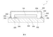
- 2 is a cross-sectional view taken along line II-II in FIG.
- FIG. 3 is a plan view of the mounting surface of the base member according to the first embodiment of the present invention.
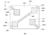
- FIG. 4 is a plan view of the mounting surface of the base member according to the modification of the first embodiment of the present invention.
- FIG. 5 is a cross-sectional view of a piezoelectric vibrator according to a second embodiment of the present invention.
- FIG. 6 is a plan view of the mounting surface of the base member according to the second embodiment of the present invention.
- FIG. 1 is an exploded perspective view of the piezoelectric vibrator
- FIG. 2 is a sectional view taken along line II-II in FIG. In FIG. 2, illustration of various electrodes of the piezoelectric vibration element is omitted.
- the piezoelectric vibrator 1 includes a piezoelectric vibration element 100, a cap 200 that is an example of a lid member, and a substrate 300 that is an example of a base member.
- the cap 200 and the substrate 300 are part of the configuration of a case or package for housing the piezoelectric vibration element 100.
- the piezoelectric vibration element 100 includes a piezoelectric substrate 110 and first and second excitation electrodes 120 and 130 formed on the piezoelectric substrate 110.
- the first excitation electrode 120 is formed on the first surface 112 of the piezoelectric substrate 110
- the second excitation electrode 130 is formed on the second surface 114 opposite to the first surface 112 of the piezoelectric substrate 110.
- the piezoelectric vibration element 100 is formed from a given piezoelectric material, and the material is not particularly limited.
- the piezoelectric vibrating element 100 is an AT-cut quartz crystal substrate and is a quartz crystal vibrating element having a rectangular piezoelectric substrate 110.
- the AT-cut quartz substrate has an X-axis, a Y-axis, and a Z-axis which are crystal axes of the artificial quartz, and the Y-axis and the Z-axis are 35 degrees 15 minutes ⁇ 1 in the direction from the Y-axis to the Z-axis around the X-axis.
- the piezoelectric substrate 110 that is an AT-cut quartz substrate has a longitudinal direction parallel to the Z′-axis direction, a short direction parallel to the X-axis direction, and a thickness direction parallel to the Y′-axis direction. And has a substantially rectangular shape on the XZ ′ plane.
- a quartz resonator element using an AT-cut quartz substrate has extremely high frequency stability over a wide temperature range, is excellent in aging characteristics, and can be manufactured at low cost.
- the AT-cut crystal resonator element often uses a thickness shear vibration mode as a main vibration.
- the piezoelectric substrate according to the present embodiment is not limited to the above-described configuration.
- a rectangular AT cut having a longitudinal direction parallel to the X-axis direction and a short direction parallel to the Z′-axis direction is used.
- a quartz substrate may be applied, a quartz substrate with a different cut other than the AT cut may be used, or other piezoelectric materials such as ceramics other than quartz may be applied.
- the piezoelectric substrate 110 has a connection electrode 124 electrically connected to the first excitation electrode 120 via the extraction electrode 122, and a connection electrode 134 electrically connected to the second excitation electrode 130 via the extraction electrode 132. And are formed. Specifically, the extraction electrode 122 is extracted from the first excitation electrode 120 toward the short side on the Z′-axis negative direction side on the first surface 112 and further passes through the side surface of the piezoelectric substrate 110 on the Z′-axis negative direction side. The connection electrode 124 formed on the second surface 114 is connected.
- the extraction electrode 132 is extracted from the second excitation electrode 130 toward the short side of the Z′-axis negative direction on the second surface 114, and is connected to the connection electrode 134 formed on the second surface 114.
- the connection electrodes 124 and 134 are disposed along the short side on the Z′-axis negative direction side, and these connection electrodes 124 and 134 are electrically connected to the substrate 300 via conductive support members 340 and 342 described later. And mechanically held.
- the arrangement and pattern shape of the connection electrodes 124 and 134 and the extraction electrodes 122 and 132 are not limited, and can be appropriately changed in consideration of electrical connection with other members.
- Each of the electrodes including the first and second excitation electrodes 120 and 130 may be formed, for example, by forming a base with a chromium (Cr) layer and forming a gold (Au) layer on the surface of the chromium layer. It is not limited.
- the cap 200 has a recess 204 that opens to face the first surface 302 of the substrate 300.
- the concave portion 204 is provided with a side wall portion 202 formed so as to rise from the bottom surface of the concave portion 204 over the entire periphery of the opening, and the side wall portion 202 is opposed to the first surface 302 of the substrate 300.
- the end surface 205 may be a front end surface of the side wall portion 202 protruding so as to rise substantially vertically from the bottom surface of the recess 204.
- the cap 200 may be formed of a conductive material such as metal, or may be formed of an insulating material such as ceramic or quartz. If the cap 200 is a conductive material, a shielding effect can be achieved by supplying a ground potential to the cap 200.
- the cap 200 may be formed of a metal, for example, the cap 200 may be formed of an alloy (for example, 42 alloy) containing iron (Fe) and nickel (Ni).
- a surface layer such as a gold (Au) layer may be further formed on the surface of the cap 200. By forming a gold layer on the surface, it is possible to prevent the cap 200 from being oxidized.
- the cap 200 may have a flange portion that protrudes further outward from the side wall portion 202. According to this, since the joint area of both can be enlarged by joining a flange part and the board
- the piezoelectric vibration element 100 is mounted on the first surface 302 (mounting surface) of the substrate 300.
- the substrate 300 has a longitudinal direction parallel to the Z′-axis direction, a short direction parallel to the X-axis direction, and a thickness direction parallel to the Y′-axis direction. It has a substantially rectangular shape on the ′ surface.
- the substrate 300 may be formed of, for example, an insulating ceramic.
- the substrate 300 may be formed of a glass material, a quartz material, a glass epoxy resin, or the like.
- the substrate 300 is preferably made of a heat resistant material.
- the substrate 300 may be a single layer or a plurality of layers.
- the substrate 300 may include an insulating layer formed on the outermost layer of the first surface 302.
- the substrate 300 may have a flat plate shape, or may have a concave shape opened in a direction facing the cap 200.
- both the cap 200 and the substrate 300 are bonded via a bonding material 350, so that the piezoelectric vibration element 100 is surrounded by an inner space (cavity) surrounded by the concave portion 204 of the cap 200 and the substrate 300. ) 206 is hermetically sealed.
- the bonding material 350 is provided over the entire circumference of the cap 200 or the substrate 300, and is interposed between the end surface 205 of the side wall 202 of the cap 200 and the first surface 302 of the substrate 300.
- the bonding material 350 includes an insulating material.
- a glass material for example, low-melting glass
- a resin material for example, an epoxy resin
- the cost is lower than that of metal bonding, the heating temperature can be suppressed, and the manufacturing process can be simplified.
- the piezoelectric vibration element 100 has one end (the end on the conductive support members 340 and 342 side) as a fixed end and the other end as a free end.
- the piezoelectric vibration element 100 may be fixed to the substrate 300 at both ends in the longitudinal direction.
- an electrode pattern 310 is formed on the first surface 302 of the substrate 300.
- the electrode pattern 310 includes connection electrodes 320 and 322 to which the piezoelectric vibration element 100 is connected, and lead electrodes 320 a and 322 a that are drawn from the connection electrodes 320 and 322 toward the outer edge of the first surface 302.
- the connection electrodes 320 and 322 are disposed on the inner side of the outer edge of the substrate 300 so that the piezoelectric vibration element 100 can be disposed substantially at the center of the first surface 302 of the substrate 300.
- connection electrode 320 is connected to the connection electrode 124 of the piezoelectric vibration element 100 via the conductive support member 340, while the connection electrode 322 is connected to the piezoelectric vibration element 100 via the conductive support member 342.
- the electrode 134 is connected.
- the conductive support members 340 and 342 support the piezoelectric vibration element 100.
- the conductive support members 340 and 342 are formed by curing a conductive adhesive.
- the extraction electrode 320a is extracted from the connection electrode 320 toward any one corner portion of the substrate 300, while the extraction electrode 322a is extracted from the connection electrode 322 toward another corner portion of the substrate 300. Yes.
- a plurality of side electrodes 330, 332, 334, and 336 are formed at each corner of the substrate 300.
- the extraction electrode 320a is in the negative X-axis direction and the negative Z′-axis direction.
- the lead electrode 322a is connected to the side electrode 332 formed in the corner portion on the X-axis positive direction side and the Z′-axis positive direction side.
- the electrode pattern 310 further includes a dummy pattern 312.
- the dummy pattern 312 is a pattern that is not electrically connected to the first and second excitation electrodes 120 and 130 of the piezoelectric vibration element 100 and is formed of the same conductive material as the other electrodes.
- the dummy pattern 312 is formed in the vicinity of the remaining corner portion (a corner portion other than the corner portion where the side electrodes 330 and 332 electrically connected to the piezoelectric vibration element 100 are disposed).
- the dummy pattern 312 it becomes easy to apply a conductive material for forming the side electrode, and the side electrode can be formed at all corners. A processing step of electrically connecting to the member is also facilitated.
- the dummy pattern 312 functions as a ground electrode to which a ground potential is supplied.
- a ground potential is supplied to the dummy pattern 312 via the side electrodes 334 and 336, and a conductive cap 200 is electrically connected to the dummy pattern 312 to provide a shielding function to the cap 200. is doing.
- the dummy pattern 312 may be connected to a terminal (terminal not connected to any other electronic element) provided on a mounting substrate (not shown) on which the piezoelectric vibrator 1 is mounted.
- the corner portion of the substrate 300 has a cut-out side surface formed by cutting a part of the corner portion into a cylindrical curved surface shape (also referred to as a castellation shape). 332, 334, and 336 are continuously formed over such a cut-out side surface and the second surface 304 (mounting surface). Note that the shape of the corner portion of the substrate 300 is not limited to this, and the shape of the cutout may be planar, or the corner of the corner portion may remain without being cutout.
- substrate 300, an extraction electrode, and a side part electrode is not limited to the above-mentioned example, It can apply in various deformation
- the connection electrodes 320 and 322 are arranged on different sides on the first surface 302 of the substrate 300 such that one is formed on the Z′-axis positive direction side and the other is formed on the Z′-axis negative direction side. It may be.
- the piezoelectric vibration element 100 is supported by the substrate 300 at both one end and the other end in the longitudinal direction.
- the number of side electrodes is not limited to four.
- a total of three side electrodes including two side electrodes electrically connected to the piezoelectric vibration element and one side electrode serving as a ground electrode. Two side electrodes may be applied.
- the side electrodes are not limited to those arranged at the corner portions, and may be formed on any side surface of the substrate 300 excluding the corner portions. In this case, as already described, a cut-out side surface obtained by cutting a part of the side surface into a cylindrical curved surface may be formed, and the side electrode may be formed on the side surface excluding the corner portion.
- FIG. 3 is a plan view of the second surface 304 of the substrate 300.
- the electrode pattern 310 has two signal electrodes (for input and output) and two ground electrodes will be described.
- the electrode pattern 310 includes signal electrodes 360 and 362, ground electrodes 364 and 366, and lead electrodes 360a, 362a, 364a, and 466a electrically connected to the electrodes.
- the signal electrodes 360 and 362 are electrically connected to the first and second excitation electrodes 120 and 130 of the piezoelectric vibrating element 100 and propagate input / output signals to the piezoelectric vibrator 1. That is, the signal electrodes 360 and 362 function as input / output electrodes of the piezoelectric vibrator 1.
- the signal electrodes 360 and 362 are disposed in a region on the second surface 304 on the side of a pair of opposing corners. Specifically, the signal electrode 360 is arranged in a region on the corner C1 side on the X-axis negative direction and the Z′-axis negative direction side, and the signal electrode 362 is a corner on the X-axis positive direction and the Z′-axis positive direction side. It is arranged in the area on the part C2 side.
- the area on the corner part C1 side is an area including the corner part C1 among four areas obtained by dividing the second surface 304 of the substrate 300 by virtual center lines 390 and 392 orthogonal to each other. Point to. The same applies to the other corner area regions.
- the signal electrode 360 is electrically connected to the side electrode 330 via an extraction electrode 360a that is extracted toward the corner portion C1 on the X-axis negative direction and the Z′-axis negative direction side.
- the signal electrode 362 is electrically connected to the side electrode 332 via an extraction electrode 362a that is extracted toward the corner portion C2 on the X-axis positive direction and the Z′-axis positive direction side.
- the signal electrodes 360 and 362 can be electrically connected to the first surface 302 side of the substrate 300 via the extraction electrodes 360 a and 362 a and the side electrodes 330 and 332, and are connected on the first surface 302.
- the first and second excitation electrodes 120 and 130 are electrically connected via the electrodes 320 and 322.
- the ground electrodes 364 and 366 are electrodes that are not electrically connected to the first and second excitation electrodes 120 and 130 of the piezoelectric vibration element 100 and are supplied with a ground potential from the outside. That is, the ground electrodes 364 and 366 function as the ground electrode of the piezoelectric vibrator 1.
- the ground electrodes 364 and 366 are arranged in a region on the other surface of the other pair of corners on the second surface 304. Specifically, the ground electrode 364 is disposed in a region on the corner portion C3 side on the X-axis negative direction and the Z′-axis positive direction side, and the ground electrode 366 is a corner on the X-axis positive direction and the Z′-axis negative direction side. It is arranged in the area on the part C4 side.
- the ground electrode 364 is electrically connected to the side electrode 334 via an extraction electrode 364a that is extracted toward the corner portion C3 on the X-axis negative direction and the Z′-axis positive direction side.
- the ground electrode 366 is electrically connected to the side electrode 336 via an extraction electrode 366a that is extracted toward the corner portion C4 on the X-axis positive direction and Z′-axis negative direction side. In this way, the ground electrodes 364 and 366 can be electrically connected to the first surface 302 side of the substrate 300 via the extraction electrodes 364a and 366a and the side electrodes 334 and 336.
- the pattern 312 is electrically connected.
- the thickness is obtained by applying an AC voltage between the pair of first and second excitation electrodes 120 and 130 in the piezoelectric vibration element 100 via the signal electrodes 360 and 362.
- the piezoelectric substrate 110 vibrates in a predetermined vibration mode such as a sliding vibration mode, and resonance characteristics associated with the vibration are obtained.
- the signal electrode 360 and the ground electrode 364 are disposed in the region on the side (first side 370) side parallel to the Z ′ axis on the X axis negative direction side, while the Z ′ on the X axis positive direction side.
- a signal electrode 362 and a ground electrode 366 are arranged in a region on the side parallel to the axis. Further, the signal electrode 360 and the ground electrode 366 are disposed in a region on the side (second side 372) parallel to the X axis on the Z ′ axis negative direction side, and on the other hand, parallel to the X axis on the Z ′ axis positive direction side.
- a signal electrode 362 and a ground electrode 364 are disposed in the side region.
- the region on the first side 370 side means that the first side 370 of the two regions obtained by dividing the second surface 304 of the substrate 300 by a virtual center line 390 parallel to the first side 370 is the first side 370. Refers to the included area. The same applies to the other side regions.
- the signal electrode 360 is a rectangular electrode, and two orthogonal sides of the signal electrode 360 are provided in parallel with the sides of the substrate 300 adjacent thereto.
- a region on the first side 370 side parallel to the Z ′ axis on the X axis negative direction side and a second side parallel to the X axis on the Z ′ axis negative direction side It is arranged in the region on the 372 side.
- the distance between the outer edge of the rectangular signal electrode 360 and the first side 370 is LX1
- the distance between the outer edge of the rectangular ground electrode 364 and the first side 370 is LX2.
- the signal electrode 360 and the ground electrode 364 are arranged so as to satisfy LX1> LX2.
- the distance between the outer edge of the signal electrode 360 and the second side 372 is LZ′1
- the distance between the outer edge of the ground electrode 366 and the second side 372 is LZ′2.
- the signal electrode 360 and the ground electrode 366 are disposed so as to satisfy LZ′1> LZ′2. That is, the signal electrode 360 is disposed on the inner side of the substrate 300 with respect to the X-axis direction and is disposed on the inner side of the substrate 300 with respect to the Z′-axis direction.
- the signal electrode 360 is disposed inside the substrate 300 with respect to the ground electrodes 364 and 366. Accordingly, even if there is a noise generation source around the piezoelectric vibrator 1, it is possible to ensure a long distance between the noise generation source and the signal electrode 360. The influence of the received noise is reduced. In addition, the influence of noise generated by the signal electrode 360 to the outside of the piezoelectric vibrator 1 can be similarly reduced.
- the signal electrode 362 is also formed on the inner side of the substrate 300 than the ground electrodes 364 and 366 in the same manner as the signal electrode 360, and the same effects as those described for the signal electrode 360 are obtained. be able to.
- the ground electrodes 364 and 366 are disposed outside the signal electrodes 360 and 362, for example, all four electrodes are uniformly disposed in the vicinity of the center of the substrate 300. As compared with the above, it is possible to suppress the occurrence of the positional deviation of the substrate 300 in the Y′-axis rotation direction and the XZ ′ plane direction and the deviation of the inclination in the Y′-axis direction when the piezoelectric vibrator 1 is mounted. Therefore, it is possible to ensure the stability when the piezoelectric vibrator 1 is mounted.
- both of the signal electrodes 360 and 362 are arranged on the inner side of the substrate 300 than the ground electrodes 364 and 366, but only one of the signal electrodes 360 and 362 is on the substrate 300. You may arrange
- the signal electrodes 360 and 362 are arranged on the inner side of the substrate 300 from the ground electrodes 364 and 366 in both the X-axis direction and the Z′-axis direction. It may be arranged inside the substrate 300 only in any one direction.
- substrate 300, a ground electrode, and an extraction electrode is not limited to the above-mentioned example, It can apply in various deformation
- the signal electrodes 360 and 362 and the ground electrodes 364 and 366 are not limited to a rectangular shape, and may have other shapes such as a circle and a polygon. The sizes of the signal electrode and the ground electrode may be different from each other.
- the signal electrode may be arranged inside the substrate with respect to the ground electrode by making the outer shape of the signal electrode smaller than the outer shape of the ground electrode.
- the total number of signal electrodes and ground electrodes is not limited to four. For example, a total of three electrodes including two signal electrodes and one ground electrode may be applied.
- the lead-out electrodes on the mounting surface side are not limited to those drawn to the corner portions, but can be appropriately changed depending on the arrangement of the side electrodes. It may be pulled out to the side electrode.
- FIG. 4 is a plan view of the second surface 304 of the substrate 303 according to a modification of the first embodiment of the present invention.
- the electrode pattern 311 further includes a connection electrode 380 on the second surface 304.
- the connection electrode 380 is formed across the signal electrode 360 and the signal electrode 362, and electrically connects the ground electrode 364 and the ground electrode 366.
- connection electrode 380 is formed by connecting the ground electrode 364 and the ground electrode 366 so as to connect the diagonal lines of the second surface 304.
- the signal electrode 360 and the signal electrode 362 are shielded by the connection electrode 380 having a ground potential, and thus one of the signal electrode 360 and the signal electrode 362 exerts on the other electrode.
- the influence of noise is reduced. Therefore, the effect of reducing the influence of noise is further improved as compared with the embodiment shown in FIG.
- FIG. 5 is a cross-sectional view of the piezoelectric vibrator 3 according to the second embodiment of the present invention
- FIG. 6 is a plan view of the base member according to the second embodiment of the present invention.
- the signal electrode 460 and the ground electrode 464 will be described as examples.
- a through electrode 490 that penetrates from the first surface 402 to the second surface 404 of the substrate 400 in a region inside the cap 200 on the substrate 400 that is an example of the base member. 492 is formed.
- the signal electrode 460 can be electrically connected to the piezoelectric vibration element 100 without using the extraction electrode on the second surface 404 of the substrate 400, for example.
- the ground electrode 464 may be electrically connected to the dummy pattern 312 on the first surface 402 of the substrate 400 via the through electrode 492.
- the signal electrode 462 and the ground electrode 466 may also be electrically connected to the first surface 402 through the through electrode, similarly to the signal electrode 460 and the ground electrode 464.
- the signal electrode and the ground electrode can be electrically connected to the piezoelectric vibrating element 100 and the dummy pattern 312 by the through electrode. Therefore, as shown in FIG. 6, the second surface 404 of the substrate 400 can be configured to have no extraction electrode corresponding to the signal electrode and the ground electrode.
- the signal electrode 360 or 362 is disposed inside the substrate 300 with respect to the ground electrode 364 or 366.
- the noise generation source around the piezoelectric vibrator 1
- the influence of is reduced.
- the influence by the noise which a signal electrode emits outside the piezoelectric vibrator 1 can be reduced similarly.
- the ground electrodes 364 and 366 are disposed outside the signal electrodes 360 and 362, the stability when the piezoelectric vibrator 1 is mounted can be ensured.
- connection electrode 380 that electrically connects the ground electrode 364 and the ground electrode 366 crosses between the signal electrode 360 and the signal electrode 362 on the second surface 304 of the substrate 300. Formed. Thereby, since the signal electrode 360 and the signal electrode 362 are shielded by the connection electrode 380 having a ground potential, the effect of reducing the influence of noise is further improved as compared with the first embodiment.
- a through electrode penetrating from the first surface 402 of the substrate 400 to the second surface 404 is formed, and the signal electrode and the ground electrode are formed on the first surface 402 of the substrate 400 through the through electrode. It is electrically connected to each electrode.
- the crystal resonator element has been described as an example of the piezoelectric resonator element.
- the present invention is not limited to this, and other piezoelectric materials such as a piezoelectric ceramic (for example, PZT) and zinc oxide are used. Also good.
- the piezoelectric vibration element may be, for example, a MEMS (Micro Electro Mechanical Systems), and may be, for example, a piezoelectric MEMS using a given piezoelectric material such as Si-MEMS, AlN, LT, or PZT. .
- the cap 200 when the cap 200 is formed of a conductive material such as metal, the cap may be maintained at the ground potential by electrically connecting the cap 200 to the ground electrode.
- a concave cap is shown as an example of the lid member.
- the present invention is not limited to this, and a flat plate-shaped lid member may be applied.
- an internal space for disposing the piezoelectric vibration element may be formed by forming the base member substrate in a concave shape.
- each embodiment described above is for facilitating understanding of the present invention, and is not intended to limit the present invention.
- the present invention can be changed / improved without departing from the spirit thereof, and the present invention includes equivalents thereof. That is, those in which the person skilled in the art appropriately changes the design of each embodiment is also included in the scope of the present invention as long as the features of the present invention are included.
- each element included in each embodiment and its arrangement, material, condition, shape, size, and the like are not limited to those illustrated, and can be changed as appropriate.
- each element included in each embodiment can be combined as much as technically possible, and combinations thereof are included in the scope of the present invention as long as they include the features of the present invention.
- 1,3 Piezoelectric vibrator 100 Piezoelectric vibration element 200 Cap (lid member) 300,400 substrate (base member) 310, 311 Electrode pattern 312 Dummy pattern 320, 322, 380 Connection electrode 320a, 322a, 360a, 362a, 364a, 366a Lead electrode 350 Bonding material 360, 362, 460, 462 Signal electrode 364, 366, 464, 466 Ground electrode 490 , 492 Through electrode
Landscapes
- Physics & Mathematics (AREA)
- Acoustics & Sound (AREA)
- Piezo-Electric Or Mechanical Vibrators, Or Delay Or Filter Circuits (AREA)
Abstract
圧電振動子(1)は、圧電振動素子(100)と、圧電振動素子(100)が搭載された搭載面(302)及び搭載面(302)とは反対の実装面(304)を有し、実装面(304)に形成された電極パターン(310)を有するベース部材(300)と、を備え、電極パターン(310)は、接地電極(364)と、圧電振動素子(100)に電気的に接続された信号電極(360)とを有し、ベース部材(300)の実装面(304)は矩形状に形成され、信号電極(360)及び接地電極(364)は、実装面(304)の外縁のうちいずれか一辺(370)側の領域に配置され、信号電極(360)の外縁から実装面(304)の一辺(370)までの距離(LX1)が、接地電極(364)の外縁から実装面(304)の一辺(370)までの距離(LX2)よりも長い。
Description
本発明は、圧電振動子に関する。
発振装置や帯域フィルタなどに用いられる圧電振動子の一態様として、例えば特許文献1には、水晶振動素子が搭載された基板と、水晶振動素子を覆うように基板に形成された金属カバーとを備える表面実装水晶振動子が開示されている。圧電振動子においては、外部からのノイズによる影響を抑えることが求められることから、特許文献1に開示される表面実装水晶振動子では、金属カバーと基板裏面に形成されたグランド端子とを、基板内に形成された貫通電極により電気的に接続して金属カバーを接地電位に保つことによって、水晶振動素子に対する外部からのノイズによる影響を抑制している。
しかし、このような従来の圧電振動子においては、金属カバーの外側からのノイズの影響を防止することはできても、基板裏面に形成された信号線端子が外部からノイズを受けたり、また、この信号線端子から外部へとノイズを発し得るという問題がある。さらに、圧電振動子においては例えば回路基板への実装性を確保することも要求される。
本発明は、このような事情に鑑みてなされたものであり、実装性を確保するとともに、信号電極が圧電振動子の外部から受けるノイズ、及び、圧電振動子の外部へと信号電極が発するノイズの影響を低減させる圧電振動子を提供することを目的とする。
本発明の一側面に係る圧電振動子は、圧電振動素子と、圧電振動素子が搭載された搭載面及び搭載面とは反対の実装面を有し、実装面に形成された電極パターンを有するベース部材と、を備え、電極パターンは、接地電極と、圧電振動素子に電気的に接続された信号電極とを有し、ベース部材の実装面は矩形状に形成され、信号電極及び接地電極は、実装面の外縁のうちいずれか一辺側の領域に配置され、信号電極の外縁から実装面の一辺までの距離が、接地電極の外縁から実装面の一辺までの距離よりも長い。
本発明によれば、実装性を確保するとともに、信号電極が圧電振動子の外部から受けるノイズ、及び、圧電振動子の外部へと信号電極が発するノイズの影響を低減させることができる。
以下に本発明の実施の形態を説明する。以下の図面の記載において、同一又は類似の構成要素は同一又は類似の符号で表している。図面は例示であり、各部の寸法や形状は模式的なものであり、本願発明の技術的範囲を当該実施の形態に限定して解するべきではない。
図1及び図2を参照しつつ、本発明の第1実施形態に係る圧電振動子を説明する。
ここで、図1は、圧電振動子の分解斜視図であり、図2は図1のII-II線断面図である。なお、図2において、圧電振動素子の各種電極の図示は省略している。
図1に示すように、本実施形態に係る圧電振動子1は、圧電振動素子100と、リッド部材の一例であるキャップ200と、ベース部材の一例である基板300と、を備える。キャップ200及び基板300は、圧電振動素子100を収容するためのケース又はパッケージの構成の一部である。
圧電振動素子100は、圧電基板110と、圧電基板110に形成された第1及び第2励振電極120,130とを含む。第1励振電極120は、圧電基板110の第1面112に形成され、また、第2励振電極130は、圧電基板110の第1面112とは反対の第2面114に形成されている。
圧電振動素子100は、所与の圧電材料から形成され、その材料は特に限定されるものではない。図1に示す例では、圧電振動素子100は、ATカット水晶基板であり、矩形状の圧電基板110を有する水晶振動素子である。ATカットの水晶基板は、人工水晶の結晶軸であるX軸、Y軸、Z軸のうち、Y軸及びZ軸をX軸の周りにY軸からZ軸の方向に35度15分±1分30秒回転させた軸をそれぞれY´軸及びZ´軸とした場合、X軸及びZ´軸によって特定される面(以下、「XZ´面」と呼ぶ。他の軸によって特定される面についても同様である。)と平行な面を主面として切り出されたものである。図1に示す例では、ATカット水晶基板である圧電基板110は、Z´軸方向に平行な長手方向と、X軸方向に平行な短手方向と、Y´軸方向に平行な厚さ方向を有しており、XZ´面において略矩形形状をなしている。ATカット水晶基板を用いた水晶振動素子は、広い温度範囲で極めて高い周波数安定性を有し、また、経時変化特性にも優れている上、低コストで製造することが可能である。また、ATカット水晶振動素子は、厚みすべり振動モード(Thickness Shear Mode)を主振動として用いられることが多い。
なお、本実施形態に係る圧電基板は上記構成に限定されるものではなく、例えば、X軸方向に平行な長手方向と、Z´軸方向に平行な短手方向とを有する矩形状のATカット水晶基板を適用してもよいし、ATカット以外の異なるカットの水晶基板であってもよいし、又は、水晶以外のセラミックなどのその他の圧電材料を適用してもよい。
第1励振電極120は、圧電基板110の第1面112(Y´軸正方向側のXZ´面)に形成され、また、第2励振電極130は、圧電基板110の第1面112とは反対の第2面114(すなわち、Y´軸負方向側のXZ´面)に形成されている。第1及び第2励振電極120,130は一対の電極であり、XZ´面の平面視において互いに重なり部分を有している。
圧電基板110には、第1励振電極120に引出電極122を介して電気的に接続された接続電極124と、第2励振電極130に引出電極132を介して電気的に接続された接続電極134とが形成されている。具体的には、引出電極122は、第1面112において第1励振電極120からZ´軸負方向側短辺に向かって引き出され、さらに圧電基板110のZ´軸負方向側の側面を通って、第2面114に形成された接続電極124に接続されている。他方、引出電極132は、第2面114において第2励振電極130からZ´軸負方向側短辺に向かって引き出され、第2面114に形成された接続電極134に接続されている。接続電極124,134は、Z´軸負方向側の短辺に沿って配置され、これらの接続電極124,134は、後述する導電性支持部材340,342を介して基板300に電気的導通を図るとともに機械的に保持される。なお、本実施形態において、接続電極124,134及び引出電極122,132の配置やパターン形状は限定されるものではなく、他の部材との電気的接続を考慮して適宜変更することができる。
第1及び第2励振電極120,130を含む上記各電極は、例えば、下地をクロム(Cr)層で形成し、クロム層の表面に金(Au)層を形成してもよく、その材料は限定されるものではない。
キャップ200は、基板300の第1面302に対向して開口した凹部204を有する。凹部204には、開口の全周に亘って、凹部204の底面から立ち上がるように形成された側壁部202が設けられており、側壁部202は、基板300の第1面302に対向する端面205を有する。図2に示すように、この端面205は、凹部204の底面から略垂直に立ち上がるように突出する側壁部202の先端面であってもよい。
キャップ200は、金属などの導電性材料によって形成されてもよいし、あるいはセラミックや水晶などの絶縁性材料によって形成されてもよい。キャップ200が導電性材料であれば、キャップ200に接地電位を供給することによってシールド効果を奏することができる。キャップ200が金属によって形成される場合、例えば、鉄(Fe)及びニッケル(Ni)を含む合金(例えば42アロイ)で形成されていてもよい。あるいは、キャップ200の表面にさらに金(Au)層などの表面層が形成されていてもよい。表面に金層を形成することによって、キャップ200の酸化防止を図ることができる。
なお、変形例として、キャップ200は、側壁部202からさらに開口外方向へ突出するフランジ部を有してもよい。これによれば、フランジ部と基板300を接合することによって、両者の接合面積を大きくすることができるため、両者の接合強度の向上を図ることができる。
基板300の第1面302(搭載面)には、圧電振動素子100が搭載される。図1に示す例では、基板300は、Z´軸方向に平行な長手方向と、X軸方向に平行な短手方向と、Y´軸方向に平行な厚さ方向を有しており、XZ´面において略矩形形状をなしている。基板300は、例えば絶縁性セラミックで形成されてもよい。あるいは、基板300は、ガラス材料、水晶材料又はガラスエポキシ樹脂などで形成してもよい。基板300は耐熱性材料から構成されることが好ましい。基板300は、単層であっても複数層であってもよく、複数層である場合、第1面302の最表層に形成された絶縁層を含んでもよい。また、基板300は、平板な板状をなしてもよいし、あるいは、キャップ200に対向する向きに開口した凹状をなしてもよい。図2に示すように、キャップ200及び基板300の両者が接合材350を介して接合されることによって、圧電振動素子100が、キャップ200の凹部204と基板300とによって囲まれた内部空間(キャビティ)206に密封封止される。
接合材350は、キャップ200又は基板300の全周に亘って設けられており、キャップ200の側壁部202の端面205と、基板300の第1面302との間に介在している。接合材350は絶縁性材料を有する。絶縁性材料としては、例えばガラス材料(例えば低融点ガラス)であってもよく、あるいは、樹脂材料(例えばエポキシ系樹脂)であってもよい。これらの絶縁性材料によれば、金属接合に比べて低コストであり、また加熱温度を抑えることができ、製造プロセスの簡易化を図ることができる。
図2に示す例では、圧電振動素子100は、その一方端(導電性支持部材340,342側の端部)が固定端であり、その他方端が自由端となっている。なお、変形例として、圧電振動素子100は、長手方向の両端において基板300に固定されていてもよい。
図1に示すように、基板300の第1面302には、電極パターン310が形成されている。電極パターン310は、圧電振動素子100が接続される接続電極320,322と、接続電極320,322から第1面302の外縁に向かって引き出される引出電極320a,322aとを含む。接続電極320,322は、圧電振動素子100が基板300の第1面302の略中央に配置することができるように、基板300の外縁よりも内側に配置されている。
接続電極320には、導電性支持部材340を介して、圧電振動素子100の接続電極124が接続され、他方、接続電極322には、導電性支持部材342を介して、圧電振動素子100の接続電極134が接続される。導電性支持部材340,342は圧電振動素子100を支持する。導電性支持部材340,342は導電性接着剤が硬化したものである。
引出電極320aは、接続電極320から基板300のいずれか1つのコーナー部に向かって引き出され、他方、引出電極322aは、接続電極322から基板300の他の1つのコーナー部に向かって引き出されている。また、基板300の各コーナー部には、複数の側部電極330,332,334,336が形成されており、図1に示す例では、引出電極320aがX軸負方向及びZ´軸負方向側のコーナー部に形成された側部電極330に接続され、他方、引出電極322aがX軸正方向及びZ´軸正方向側のコーナー部に形成された側部電極332に接続されている。
本実施形態では、電極パターン310は、ダミーパターン312をさらに含む。ダミーパターン312は、圧電振動素子100の第1及び第2励振電極120,130とは電気的に接続されることがないパターンであり、他の電極と同じ導電材料によって形成されている。ダミーパターン312は、残りのコーナー部(圧電振動素子100と電気的に接続された側部電極330,332が配置されたコーナー部以外のコーナー部)付近に形成されている。ダミーパターン312を形成することにより、側部電極を形成するための導電材料の付与が容易になり、また、全てのコーナー部に側部電極を形成することができるため、圧電振動子を他の部材に電気的に接続する処理工程も容易となる。ダミーパターン312は、接地電位が供給される接地電極として機能する。この場合、側部電極334,336を経由してダミーパターン312に接地電位を供給するとともに、かかるダミーパターン312に導電性のキャップ200を電気的に接続することによって、キャップ200にシールド機能を付与している。なお、ダミーパターン312は、圧電振動子1が実装される実装基板(図示しない)に設けられた端子(他のいずれの電子素子とも接続されない端子)に接続されてもよい。
図1に示す例では、基板300のコーナー部は、その一部が円筒曲面状(キャスタレーション形状とも呼ばれる。)に切断して形成された切り欠き側面を有しており、側部電極330,332,334,336は、このような切り欠き側面及び第2面304(実装面)にかけて連続的に形成されている。なお、基板300のコーナー部の形状はこれに限定されるものではなく、切り欠きの形状は平面状であってもよいし、切り欠きがなく、コーナー部の角が残っていてもよい。
なお、基板300の接続電極、引出電極及び側部電極の各構成は上述の例に限定されるものではなく、様々に変形して適用することができる。例えば、接続電極320,322は、一方がZ´軸正方向側に形成され、他方がZ´軸負方向側に形成されるなど、基板300の第1面302上において互いに異なる側に配置されていてもよい。このような構成においては、圧電振動素子100が、長手方向の一方端及び他方端の両方において基板300に支持されることになる。また、側部電極の個数は4つに限るものではなく、例えば圧電振動素子に電気的に接続された2つの側部電極と、接地用の電極である1つの側部電極とを有する合計3つの側部電極を適用してもよい。また、側部電極はコーナー部に配置されたものに限らず、コーナー部を除く基板300のいずれかの側面に形成されてもよい。この場合、既に説明したとおり、側面の一部を円筒曲面状に切断した切り欠き側面を形成し、コーナー部を除く当該側面に側部電極を形成してもよい。
次に、図3を参照して、基板300の第2面304(実装面)に形成された電極パターン310の構成についてさらに詳述する。ここで、図3は、基板300の第2面304の平面図である。なお、以下では、電極パターン310が2つの信号電極(入力用及び出力用)及び2つの接地電極を有する態様を説明する。
図3に示すように、電極パターン310は、信号電極360,362と、接地電極364,366、及び、各電極に電気的に接続された引出電極360a,362a,364a,466aを有する。
信号電極360,362は、圧電振動素子100の第1及び第2励振電極120,130に電気的に接続されており、圧電振動子1に対する入出力信号を伝搬するものである。すなわち、信号電極360,362は、圧電振動子1の入出力電極として機能する。
信号電極360,362は、第2面304上の対向する一対のコーナー部側の領域に配置されている。具体的には、信号電極360はX軸負方向及びZ´軸負方向側のコーナー部C1側の領域に配置され、また、信号電極362はX軸正方向及びZ´軸正方向側のコーナー部C2側の領域に配置されている。ここで、例えば、コーナー部C1側の領域とは、基板300の第2面304を、互いに直交する仮想中心線390,392によって分割した4つの領域のうち、当該コーナー部C1が含まれる領域を指す。このことは他のコーナー部側の領域についても同様である。
信号電極360は、X軸負方向及びZ´軸負方向側のコーナー部C1に向かって引き出された引出電極360aを介して側部電極330に電気的に接続されている。また、信号電極362は、X軸正方向及びZ´軸正方向側のコーナー部C2に向かって引き出された引出電極362aを介して側部電極332に電気的に接続されている。こうして、信号電極360,362は、引出電極360a,362a及び側部電極330,332を介して、基板300の第1面302側に電気的に導通可能となっており、第1面302において接続電極320,322を介して第1及び第2励振電極120,130に電気的に接続されている。
接地電極364,366は、圧電振動素子100の第1及び第2励振電極120,130とは電気的に接続されておらず、外部から接地電位が供給されるための電極である。すなわち、接地電極364,366は、圧電振動子1の接地電極として機能する。
接地電極364,366は、第2面304上の対向する他の一対のコーナー部側の領域に配置されている。具体的には、接地電極364はX軸負方向及びZ´軸正方向側のコーナー部C3側の領域に配置され、また、接地電極366はX軸正方向及びZ´軸負方向側のコーナー部C4側の領域に配置されている。
接地電極364は、X軸負方向及びZ´軸正方向側のコーナー部C3に向かって引き出された引出電極364aを介して側部電極334に電気的に接続されている。また、接地電極366は、X軸正方向及びZ´軸負方向側のコーナー部C4に向かって引き出された引出電極366aを介して側部電極336に電気的に接続されている。こうして、接地電極364,366は、引出電極364a,366a及び側部電極334,336を介して、基板300の第1面302側に電気的に導通可能となっており、第1面302においてダミーパターン312と電気的に接続されている。
本実施形態に係る圧電振動子1においては、信号電極360,362を介して、圧電振動素子100における一対の第1及び第2励振電極120,130の間に交流電圧を印加することにより、厚みすべり振動モードなどの所定の振動モードで圧電基板110が振動し、該振動に伴う共振特性が得られる。
本実施形態においては、X軸負方向側のZ´軸と平行する辺(第1辺370)側の領域に信号電極360及び接地電極364が配置され、他方、X軸正方向側のZ´軸と平行する辺側の領域に信号電極362及び接地電極366が配置されている。また、Z´軸負方向側のX軸と平行する辺(第2辺372)側の領域に信号電極360及び接地電極366が配置され、他方、Z´軸正方向側のX軸と平行する辺側の領域に信号電極362及び接地電極364が配置されている。なお、例えば、第1辺370側の領域とは、基板300の第2面304を、当該第1辺370と平行な仮想中心線390によって分割した2つの領域のうち、当該第1辺370が含まれる領域を指す。このことは他の辺側の領域についても同様である。
次に、接地電極に対する信号電極の相対的な配置について、信号電極360を例として説明する。図3に示されるように、信号電極360は矩形状の電極であって、信号電極360の直交する2辺はそれぞれと隣接する基板300の辺と平行に設けられている。基板300の第2面304の外縁のうち、X軸負方向側のZ´軸と平行する第1辺370側の領域であって、Z´軸負方向側のX軸と平行する第2辺372側の領域に配置される。ここで、X軸方向について、矩形状の信号電極360の外縁と第1辺370との距離をLX1、矩形状の接地電極364の外縁と第1辺370との距離をLX2とする。このとき、LX1>LX2を満たすように信号電極360及び接地電極364が配置されている。また、Z´軸方向について、信号電極360の外縁と第2辺372との距離をLZ´1、接地電極366の外縁と第2辺372との距離をLZ´2とする。このとき、LZ´1>LZ´2を満たすように信号電極360及び接地電極366が配置されている。すなわち、信号電極360は、X軸方向について接地電極364よりも基板300の内側に配置され、また、Z´軸方向について接地電極366よりも基板300の内側に配置されている。
以上のとおり、本実施形態においては、信号電極360が接地電極364,366よりも基板300の内側に配置されている。これによって、圧電振動子1の周囲にノイズの発生源が存在しても、ノイズの発生源と信号電極360との距離を長く確保することができ、信号電極360が圧電振動子1の外部から受けるノイズの影響が低減される。また、信号電極360が圧電振動子1の外部へと発するノイズによる影響も、同様に低減させることができる。
なお、本実施形態においては、信号電極362についても信号電極360と同様に、接地電極364,366よりも基板300の内側に形成されており、信号電極360について説明した内容と同様の効果を得ることができる。
また、本実施形態においては、接地電極364,366が信号電極360,362よりも外側に配置されることになるため、例えば4つ全ての電極を基板300の中央近辺に一様に配置する態様と比べて、圧電振動子1の実装時における基板300のY´軸回転方向及びXZ´平面方向の位置ずれ、及びY´軸方向の傾きのずれが発生することを抑制することができる。従って、圧電振動子1の実装時の安定性を確保することができる。
図3に示す例においては、信号電極360,362のいずれもが接地電極364,366より基板300の内側に配置されているが、信号電極360,362のいずれか一方の電極のみが基板300の内側に配置されていてもよい。また、図3に示す例においては、信号電極360,362について、X軸方向及びZ´軸方向ともに接地電極364,366より基板300の内側に配置されているが、X軸方向又はZ´軸方向のいずれか一方向についてのみ基板300の内側に配置されていてもよい。
なお、基板300の信号電極、接地電極及び引出電極の各構成は、上述の例に限定されるものではなく、様々に変形して適用することができる。例えば、信号電極360,362及び接地電極364,366は、矩形状に限らず、円形や多角形等の他の形状であってもよい。また、信号電極及び接地電極の大きさがそれぞれ異なっても良い。例えば、信号電極の外形を接地電極の外形よりも小さいサイズにすることによって、信号電極を接地電極よりも基板の内側に配置してもよい。さらに、信号電極及び接地電極の個数は合計4つに限るものではなく、例えば2つの信号電極と1つの接地電極から成る合計3つの電極を適用してもよい。また、実装面側の引出電極はコーナー部に引き出されたものに限らず、側部電極の配置によって適宜変更することが可能であり、例えばコーナー部を除く基板300のいずれかの側面に形成された側部電極に引き出されてもよい。
次に、図4を参照して、第1実施形態に係る圧電振動子の変形例を説明する。なお、以降の変形例及び実施形態においては、第1実施形態と共通の事柄についての記述を省略し、異なる点についてのみ説明する。特に、同様の構成による同様の作用効果については実施形態毎には逐次言及しない。
図4は、本発明の第1実施形態の変形例に係る基板303の第2面304の平面図である。本実施例では、電極パターン311は、第2面304上に接続電極380をさらに有する。接続電極380は、信号電極360と信号電極362の間を横切って形成され、接地電極364と接地電極366を電気的に接続する。
本変形例では図4に示すように、接続電極380は、接地電極364と接地電極366を第2面304の対角線で結ぶように接続して形成されている。
これにより、第2面304上において、信号電極360と信号電極362が、接地電位を帯びた接続電極380によって遮蔽されるため、信号電極360と信号電極362の一方の電極が他方の電極に及ぼすノイズの影響が低減される。従って、図3に示す態様に比べて、ノイズの影響を低減する効果がより向上する。
次に、図5、図6を参照して、本発明の第2実施形態に係る圧電振動子3を説明する。
図5は、本発明の第2実施形態に係る圧電振動子3の断面図であり、また、図6は、本発明の第2実施形態に係るベース部材の平面図である。以下に、信号電極460及び接地電極464を例として説明する。
本実施形態では、図5に示されるように、ベース部材の一例である基板400に、キャップ200の内側の領域において、基板400の第1面402から第2面404へ貫通する貫通電極490,492が形成されている。これにより、圧電振動素子100が搭載された第1面402から、第1面402とは反対の面である第2面404へ電気的導通が図られている。これによれば、信号電極460を、例えば、基板400の第2面404における引出電極を介さずに、圧電振動素子100に電気的に接続することができる。また、接地電極464についても、貫通電極492を介して基板400の第1面402上のダミーパターン312に電気的に接続してもよい。なお、信号電極462及び接地電極466についても信号電極460及び接地電極464と同様に、貫通電極を介して第1面402への電気的導通を図ってもよい。
本実施形態においては、上記貫通電極によって信号電極及び接地電極を圧電振動素子100及びダミーパターン312と電気的に接続することができる。そのため、図6に示されるように、基板400の第2面404において、信号電極及び接地電極に対応する引出電極を有さない構成とすることができる。
本実施形態においても、第1実施形態と同様の効果を得ることができる。
以上、本発明の例示的な実施形態について説明した。圧電振動子1では、信号電極360又は362が、接地電極364又は366よりも基板300の内側に配置される。これにより、圧電振動子1の周囲にノイズの発生源が存在しても、ノイズの発生源と信号電極との距離を長く確保することができ、信号電極が圧電振動子1の外部から受けるノイズの影響が低減される。また、信号電極が圧電振動子1の外部へと発するノイズによる影響も同様に低減させることができる。また、接地電極364,366が信号電極360,362よりも外側に配置されることになるため、圧電振動子1の実装時の安定性を確保することができる。
また、第1実施形態の変形例では、基板300の第2面304上において、接地電極364と接地電極366を電気的に接続する接続電極380が、信号電極360と信号電極362の間を横切って形成される。これにより、信号電極360と信号電極362が、接地電位を帯びた接続電極380によって遮蔽されるため、第1実施形態に比べてノイズの影響を低減する効果がより向上する。
また、第2実施形態では、基板400の第1面402から第2面404へ貫通する貫通電極が形成され、貫通電極を介して、信号電極及び接地電極が基板400の第1面402上の各電極に電気的に接続される。これにより、例えば第2面404に引出電極を形成することなく、第1実施形態と同様の効果を得ることができる。
なお、上記実施形態では圧電振動素子の一例として水晶振動素子を説明したが、本発明はこれに限定されるものではなく、圧電セラミック(例えばPZT)や酸化亜鉛などのその他の圧電材料を用いてもよい。また、圧電振動素子は、例えばMEMS(Micro Electro Mechanical Systems)であってもよく、例えば、Si-MEMSや、AlN、LT、PZTなどの所与の圧電材料を用いた圧電MEMSであってもよい。
また、上記全ての実施形態において、キャップ200が金属などの導電性材料によって形成された場合、キャップ200を接地電極と電気的に接続することでキャップを接地電位に維持してもよい。
また、上記実施形態ではリッド部材の一例として、凹状のキャップを示したが、本発明はこれに限定されず、平板な板状のリッド部材を適用してもよい。この場合、ベース部材の基板を凹状に形成することによって圧電振動素子を配置するための内部空間を形成するようにしてもよい。
なお、以上説明した各実施形態は、本発明の理解を容易にするためのものであり、本発明を限定して解釈するためのものではない。本発明は、その趣旨を逸脱することなく、変更/改良され得るととともに、本発明にはその等価物も含まれる。すなわち、各実施形態に当業者が適宜設計変更を加えたものも、本発明の特徴を備えている限り、本発明の範囲に包含される。例えば、各実施形態が備える各要素およびその配置、材料、条件、形状、サイズなどは、例示したものに限定されるわけではなく適宜変更することができる。また、各実施形態が備える各要素は、技術的に可能な限りにおいて組み合わせることができ、これらを組み合わせたものも本発明の特徴を含む限り本発明の範囲に包含される。
1,3 圧電振動子
100 圧電振動素子
200 キャップ(リッド部材)
300,400 基板(ベース部材)
310,311 電極パターン
312 ダミーパターン
320,322,380 接続電極
320a,322a,360a,362a,364a,366a 引出電極
350 接合材
360,362,460,462 信号電極
364,366,464,466 接地電極
490,492 貫通電極
100 圧電振動素子
200 キャップ(リッド部材)
300,400 基板(ベース部材)
310,311 電極パターン
312 ダミーパターン
320,322,380 接続電極
320a,322a,360a,362a,364a,366a 引出電極
350 接合材
360,362,460,462 信号電極
364,366,464,466 接地電極
490,492 貫通電極
Claims (9)
- 圧電振動素子と、
前記圧電振動素子が搭載された搭載面及び前記搭載面とは反対の実装面を有し、前記実装面に形成された電極パターンを有するベース部材と、
を備え、
前記電極パターンは、接地電極と、前記圧電振動素子に電気的に接続された信号電極とを有し、
前記ベース部材の前記実装面は矩形状に形成され、
前記信号電極及び前記接地電極は、前記実装面の外縁のうちいずれか一辺側の領域に配置され、
前記信号電極の外縁から前記実装面の前記一辺までの距離が、前記接地電極の外縁から前記実装面の前記一辺までの距離よりも長い、
圧電振動子。 - 前記電極パターンは、第1及び第2の接地電極を前記接地電極として有し、第1及び第2の信号電極の少なくとも一方を前記信号電極として有する、
請求項1に記載の圧電振動子。 - 前記第1及び第2の接地電極は、前記実装面の対向する一対のコーナー部側の領域に配置され、
前記第1及び第2の信号電極は、前記実装面の対向する他の一対のコーナー部側の領域に配置された、
請求項2に記載の圧電振動子。 - 前記電極パターンは、前記第1及び第2の接地電極と前記第1及び第2の信号電極のうち、少なくとも一つの電極に電気的に接続された引出電極をさらに有する、
請求項2又は3に記載の圧電振動子。 - 前記電極パターンは、前記第1及び第2の接地電極と前記第1及び第2の信号電極のうち、少なくとも一つの電極を、前記ベース部材の前記搭載面側に電気的に導通させる貫通電極をさらに有する、
請求項2又は3に記載の圧電振動子。 - 前記電極パターンは、前記第1の接地電極と前記第2の接地電極を電気的に接続する接続電極をさらに有し、
前記接続電極は、前記実装面上において前記第1の信号電極と前記第2の信号電極の間を横切って形成された、
請求項2~5のいずれか一項に記載の圧電振動子。 - 前記圧電振動素子を封止するように前記ベース部材の前記搭載面に接合されたリッド部材をさらに備えた、
請求項2~6のいずれか一項に記載の圧電振動子。 - 前記リッド部材は金属によって形成され、
前記第1及び第2の接地電極は、前記リッド部材に電気的に接続された、
請求項7に記載の圧電振動子。 - 前記圧電振動素子は水晶振動素子である、
請求項1~8のいずれか一項に記載の圧電振動子。
Priority Applications (2)
| Application Number | Priority Date | Filing Date | Title |
|---|---|---|---|
| JP2017546418A JP6739759B2 (ja) | 2015-10-21 | 2016-06-06 | 圧電振動子 |
| US15/948,228 US10985727B2 (en) | 2015-10-21 | 2018-04-09 | Piezoelectric vibrator |
Applications Claiming Priority (2)
| Application Number | Priority Date | Filing Date | Title |
|---|---|---|---|
| JP2015207239 | 2015-10-21 | ||
| JP2015-207239 | 2015-10-21 |
Related Child Applications (1)
| Application Number | Title | Priority Date | Filing Date |
|---|---|---|---|
| US15/948,228 Continuation US10985727B2 (en) | 2015-10-21 | 2018-04-09 | Piezoelectric vibrator |
Publications (1)
| Publication Number | Publication Date |
|---|---|
| WO2017068809A1 true WO2017068809A1 (ja) | 2017-04-27 |
Family
ID=58557210
Family Applications (1)
| Application Number | Title | Priority Date | Filing Date |
|---|---|---|---|
| PCT/JP2016/066781 Ceased WO2017068809A1 (ja) | 2015-10-21 | 2016-06-06 | 圧電振動子 |
Country Status (3)
| Country | Link |
|---|---|
| US (1) | US10985727B2 (ja) |
| JP (1) | JP6739759B2 (ja) |
| WO (1) | WO2017068809A1 (ja) |
Cited By (1)
| Publication number | Priority date | Publication date | Assignee | Title |
|---|---|---|---|---|
| DE112022004421T5 (de) | 2021-11-29 | 2024-07-04 | Misumi Corporation | Abschätzungssystem, abschätzungsprogramm und steuerungsverfahren für abschätzungssystem |
Families Citing this family (2)
| Publication number | Priority date | Publication date | Assignee | Title |
|---|---|---|---|---|
| JP6075701B1 (ja) * | 2015-09-11 | 2017-02-08 | 株式会社安川電機 | 電気機器及び電力変換装置 |
| CN113654583B (zh) * | 2021-08-31 | 2022-05-06 | 西安交通大学 | 剪切式振动-超声复合传感器及测量装置 |
Citations (3)
| Publication number | Priority date | Publication date | Assignee | Title |
|---|---|---|---|---|
| JP2000165086A (ja) * | 1998-11-30 | 2000-06-16 | Kinseki Ltd | 電子部品容器 |
| JP2010073907A (ja) * | 2008-09-19 | 2010-04-02 | Daishinku Corp | 電子部品用パッケージ、電子部品用パッケージのベース |
| JP2014030079A (ja) * | 2012-07-31 | 2014-02-13 | Daishinku Corp | 圧電発振器 |
Family Cites Families (8)
| Publication number | Priority date | Publication date | Assignee | Title |
|---|---|---|---|---|
| JPH11298281A (ja) * | 1998-04-16 | 1999-10-29 | Toyo Commun Equip Co Ltd | 表面実装型圧電デバイス及び圧電ユニット |
| JP2008104095A (ja) * | 2006-10-20 | 2008-05-01 | Epson Toyocom Corp | 圧電振動子、圧電デバイスおよび電子機器 |
| CN101790787B (zh) * | 2007-08-23 | 2012-07-18 | 株式会社大真空 | 电子部件用封装、电子部件用封装的基底、以及电子部件用封装与电路基板的接合结构 |
| JP4744578B2 (ja) * | 2008-09-24 | 2011-08-10 | 日本電波工業株式会社 | 恒温型の水晶発振器 |
| JP2013192052A (ja) * | 2012-03-14 | 2013-09-26 | Nippon Dempa Kogyo Co Ltd | 水晶デバイス及びその製造方法。 |
| JP2015128276A (ja) * | 2013-11-29 | 2015-07-09 | 日本電波工業株式会社 | 表面実装水晶振動子及びその製造方法 |
| JP6309757B2 (ja) * | 2013-12-26 | 2018-04-11 | 京セラ株式会社 | 水晶デバイス |
| JP6819528B2 (ja) * | 2017-09-26 | 2021-01-27 | トヨタ自動車株式会社 | ロータ |
-
2016
- 2016-06-06 JP JP2017546418A patent/JP6739759B2/ja not_active Expired - Fee Related
- 2016-06-06 WO PCT/JP2016/066781 patent/WO2017068809A1/ja not_active Ceased
-
2018
- 2018-04-09 US US15/948,228 patent/US10985727B2/en active Active
Patent Citations (3)
| Publication number | Priority date | Publication date | Assignee | Title |
|---|---|---|---|---|
| JP2000165086A (ja) * | 1998-11-30 | 2000-06-16 | Kinseki Ltd | 電子部品容器 |
| JP2010073907A (ja) * | 2008-09-19 | 2010-04-02 | Daishinku Corp | 電子部品用パッケージ、電子部品用パッケージのベース |
| JP2014030079A (ja) * | 2012-07-31 | 2014-02-13 | Daishinku Corp | 圧電発振器 |
Cited By (1)
| Publication number | Priority date | Publication date | Assignee | Title |
|---|---|---|---|---|
| DE112022004421T5 (de) | 2021-11-29 | 2024-07-04 | Misumi Corporation | Abschätzungssystem, abschätzungsprogramm und steuerungsverfahren für abschätzungssystem |
Also Published As
| Publication number | Publication date |
|---|---|
| US20180234077A1 (en) | 2018-08-16 |
| JPWO2017068809A1 (ja) | 2018-08-09 |
| JP6739759B2 (ja) | 2020-08-12 |
| US10985727B2 (en) | 2021-04-20 |
Similar Documents
| Publication | Publication Date | Title |
|---|---|---|
| JP6338205B2 (ja) | 圧電発振器及び圧電発振デバイス | |
| JP6562320B2 (ja) | 水晶振動子及びその温度制御方法、並びに水晶発振器 | |
| CN109314502B (zh) | 水晶振动元件、水晶振子以及水晶振动元件的制造方法 | |
| JP6281734B2 (ja) | 圧電振動子及びその製造方法 | |
| JP6663599B2 (ja) | 圧電振動子及び圧電振動子の製造方法 | |
| CN108352820B (zh) | 压电振动器件 | |
| JP6739759B2 (ja) | 圧電振動子 | |
| JP6288533B2 (ja) | 圧電振動子 | |
| JP2015173366A (ja) | 圧電振動片及び圧電デバイス | |
| US11233497B2 (en) | Piezoelectric vibrator | |
| CN109690940B (zh) | 水晶振子及其制造方法 | |
| JP2017038227A (ja) | 電子部品及びその製造方法 | |
| WO2016132766A1 (ja) | 水晶振動子及び水晶振動デバイス | |
| JP6555500B2 (ja) | 圧電振動素子及び圧電振動子 | |
| WO2020195818A1 (ja) | 振動素子、振動子及び振動素子の製造方法 | |
| JP7061275B2 (ja) | 水晶振動素子および水晶振動子 | |
| WO2017213163A1 (ja) | 圧電振動素子 | |
| JP4833716B2 (ja) | 圧電発振器 | |
| WO2017169864A1 (ja) | 圧電振動子 | |
| WO2016181882A1 (ja) | 水晶振動素子及び水晶振動子 | |
| JP2017123616A (ja) | 圧電振動子 |
Legal Events
| Date | Code | Title | Description |
|---|---|---|---|
| 121 | Ep: the epo has been informed by wipo that ep was designated in this application |
Ref document number: 16857127 Country of ref document: EP Kind code of ref document: A1 |
|
| ENP | Entry into the national phase |
Ref document number: 2017546418 Country of ref document: JP Kind code of ref document: A |
|
| NENP | Non-entry into the national phase |
Ref country code: DE |
|
| 122 | Ep: pct application non-entry in european phase |
Ref document number: 16857127 Country of ref document: EP Kind code of ref document: A1 |