WO2017065019A1 - 固体撮像素子、および電子装置 - Google Patents
固体撮像素子、および電子装置 Download PDFInfo
- Publication number
- WO2017065019A1 WO2017065019A1 PCT/JP2016/078982 JP2016078982W WO2017065019A1 WO 2017065019 A1 WO2017065019 A1 WO 2017065019A1 JP 2016078982 W JP2016078982 W JP 2016078982W WO 2017065019 A1 WO2017065019 A1 WO 2017065019A1
- Authority
- WO
- WIPO (PCT)
- Prior art keywords
- solid
- photoelectric conversion
- charge
- holding
- state imaging
- Prior art date
- Legal status (The legal status is an assumption and is not a legal conclusion. Google has not performed a legal analysis and makes no representation as to the accuracy of the status listed.)
- Ceased
Links
Images










Classifications
-
- H—ELECTRICITY
- H04—ELECTRIC COMMUNICATION TECHNIQUE
- H04N—PICTORIAL COMMUNICATION, e.g. TELEVISION
- H04N25/00—Circuitry of solid-state image sensors [SSIS]; Control thereof
- H04N25/60—Noise processing, e.g. detecting, correcting, reducing or removing noise
- H04N25/62—Detection or reduction of noise due to excess charges produced by the exposure, e.g. smear, blooming, ghost image, crosstalk or leakage between pixels
-
- H—ELECTRICITY
- H04—ELECTRIC COMMUNICATION TECHNIQUE
- H04N—PICTORIAL COMMUNICATION, e.g. TELEVISION
- H04N25/00—Circuitry of solid-state image sensors [SSIS]; Control thereof
- H04N25/70—SSIS architectures; Circuits associated therewith
- H04N25/76—Addressed sensors, e.g. MOS or CMOS sensors
-
- H—ELECTRICITY
- H04—ELECTRIC COMMUNICATION TECHNIQUE
- H04N—PICTORIAL COMMUNICATION, e.g. TELEVISION
- H04N25/00—Circuitry of solid-state image sensors [SSIS]; Control thereof
- H04N25/70—SSIS architectures; Circuits associated therewith
- H04N25/76—Addressed sensors, e.g. MOS or CMOS sensors
- H04N25/77—Pixel circuitry, e.g. memories, A/D converters, pixel amplifiers, shared circuits or shared components
-
- H—ELECTRICITY
- H10—SEMICONDUCTOR DEVICES; ELECTRIC SOLID-STATE DEVICES NOT OTHERWISE PROVIDED FOR
- H10F—INORGANIC SEMICONDUCTOR DEVICES SENSITIVE TO INFRARED RADIATION, LIGHT, ELECTROMAGNETIC RADIATION OF SHORTER WAVELENGTH OR CORPUSCULAR RADIATION
- H10F39/00—Integrated devices, or assemblies of multiple devices, comprising at least one element covered by group H10F30/00, e.g. radiation detectors comprising photodiode arrays
- H10F39/10—Integrated devices
- H10F39/12—Image sensors
-
- H—ELECTRICITY
- H10—SEMICONDUCTOR DEVICES; ELECTRIC SOLID-STATE DEVICES NOT OTHERWISE PROVIDED FOR
- H10F—INORGANIC SEMICONDUCTOR DEVICES SENSITIVE TO INFRARED RADIATION, LIGHT, ELECTROMAGNETIC RADIATION OF SHORTER WAVELENGTH OR CORPUSCULAR RADIATION
- H10F39/00—Integrated devices, or assemblies of multiple devices, comprising at least one element covered by group H10F30/00, e.g. radiation detectors comprising photodiode arrays
- H10F39/10—Integrated devices
- H10F39/12—Image sensors
- H10F39/18—Complementary metal-oxide-semiconductor [CMOS] image sensors; Photodiode array image sensors
Definitions
- the present disclosure relates to a solid-state imaging device and an electronic device, and more particularly to a solid-state imaging device and an electronic device that can remove noise components due to stray light.
- CMOS image sensor (hereinafter abbreviated as CIS) is a rolling shutter system in which the exposure timing of each pixel is shifted for each row.
- CIS CMOS image sensor
- focal plane distortion occurs when an image of a fast-moving subject is imaged. Therefore, a global shutter system that can unify the exposure timing of all pixels has been developed.
- the CIS adopting the global shutter system transfers signal charges from a PD (photodiode) that performs photoelectric conversion according to incident light to an FD (floating diffusion) as a charge holding unit, and the FD is until the next readout period. It has a structure for holding the transferred signal charge.
- the signal charge converted from incident light by the PD is transferred and held in the FD via the transfer transistor and the first switch.
- noise charges generated by stray light in the PD are transferred and held via the transfer transistor and the second switch.
- the present disclosure has been made in view of such a situation, and accurately extracts a noise component that can be appropriately removed from a stray light that may occur in a global shutter type solid-state imaging device. .
- a solid-state imaging device is a global shutter-type solid-state imaging device in which an exposure period of all pixels is unified, and a photoelectric conversion unit that generates charge according to incident light for each pixel;
- An accumulator that accumulates the signal charge generated by the converter and converts it into an electrical signal, and is arranged in series between the photoelectric converter and the accumulator, and the signal charge generated by the photoelectric converter is First and second holding units that temporarily hold and then transfer to the storage unit, and one of the first and second holding units holds the signal charge generated by the photoelectric conversion unit And the other of the first and second holding units does not hold the signal charge generated by the photoelectric conversion unit. ,input It used in applications for holding the noise charges.
- the solid-state imaging device may further include an OFG that resets the photoelectric conversion unit by discharging the charge remaining in the photoelectric conversion unit.
- the first and second holding units can be composed of a CCD.
- the equivalent noise charges generated in the photoelectric conversion unit due to stray light can be input to the first and second holding units.
- the first and second holding units can be arranged at symmetrical positions with respect to the condensing center of the photoelectric conversion unit.
- the solid-state imaging device has an electric signal level based on the signal charge in a state where the noise charge is superimposed, which is held in one of the first and second holding units.
- a first pixel driving process acquired after an electric signal level based on the noise charge held in the other of the first and second holding units, and held in one of the first and second holding units
- the electric signal level based on the signal charge in a state where the noise charge is superimposed is acquired before the electric signal level based on the noise charge held in the other of the first and second holding units.
- the second pixel driving process can be executed.
- the first pixel driving process and the second pixel driving process can be executed alternately for each frame.
- the first pixel driving process and the second pixel driving process can be executed alternately every predetermined time.
- Pixels of the same color in the same row or the same column are arranged such that the positional relationship between the first and second holding units arranged at symmetrical positions with respect to the light collecting center of the photoelectric conversion unit is switched. Can do.
- the solid-state imaging device has an electric signal level based on the signal charge in a state where the noise charge is superimposed, which is held in one of the first and second holding units.
- a first pixel driving process acquired after an electric signal level based on the noise charge held in the other of the first and second holding units, or held in one of the first and second holding units An electric signal level based on the signal charge in a state where the noise charge is superimposed before an electric signal level based on the noise charge held in the other of the first and second holding units.
- the second pixel driving process to be acquired can be executed.
- the solid-state imaging device that is one aspect of the present disclosure can be a back-illuminated type.
- the solid-state imaging device which is one aspect of the present disclosure can be a surface irradiation type.
- the storage unit can be shared by a plurality of pixels.
- An electronic device is an electronic device including a global shutter type solid-state imaging device in which an exposure period of all pixels is unified, and the solid-state imaging device has a charge corresponding to incident light for each pixel.
- the photoelectric conversion unit that generates the photoelectric conversion unit
- the storage unit that accumulates the signal charges generated by the photoelectric conversion unit and converts them into an electrical signal
- a first holding unit that temporarily holds the signal charge generated by the conversion unit and then transfers the signal charge to the storage unit, wherein one of the first and second holding units is the photoelectric conversion unit Used for holding the input noise charge while holding the signal charge generated by the unit, the other of the first and second holding units being generated by the photoelectric conversion unit Trust In a state that does not hold a charge, it is used in applications for holding the inputted noise charges.
- a first and a second are arranged in series between the photoelectric conversion unit and the storage unit, and temporarily transfer the signal charge generated by the photoelectric conversion unit to the storage unit after the signal charge is temporarily held.
- One of the holding units holds the signal charge generated by the photoelectric conversion unit, and the input noise charge is also held.
- the other of the first and second holding units is the photoelectric conversion The signal charge generated by the unit is held.
- the noise component can be accurately extracted so that the noise component due to stray light can be appropriately removed.
- FIG. 1 is an equivalent circuit diagram showing a configuration example for one pixel of the solid-state imaging device according to the present embodiment. Note that the solid-state imaging device according to the present embodiment can be applied to either a backside illumination type or a frontside illumination type.
- the solid-state imaging device includes a PD (photodiode) 11, an OFG (overflow gate) 12, a first memory (MEM1) 13, a second memory (MEM2) 14, a transfer gate (TG) 15, and an FD (floating diffusion) 16. , RST transistor 17, AMP transistor 18, and SEL transistor 19.
- PD 11 is a photoelectric conversion element that receives incident light and performs photoelectric conversion by accumulating electric charge corresponding to the incident light.
- PD 11 has its anode connected to GND (grounded) and its cathode connected to transfer gate 15 via first memory 13 and second memory 14.
- the OFG 12 is driven when the charge remaining in the PD 11 in the initial state is discharged to the overflow drain.
- One of the first memory 13 and the second memory 14 is used for the purpose of holding a noise charge caused by stray light while holding the signal charge converted by the PD 11.
- the other of the first memory 13 and the second memory 14 is used for the purpose of holding noise charge caused by stray light in a state where the signal charge converted by the PD 11 is not held.
- a CCD Charge Coupled Device
- the charges accumulated in the first memory 13 and the second memory 14 can be completely transferred to the subsequent stage.
- the transfer gate 15 is driven when the signal charge converted by the PD 11 is transferred to the FD 16.
- the FD 16 is a region formed at a connection point between the transfer gate 15 and the RST transistor 17. In the FD 16, charges supplied thereto are converted into a voltage.
- the RST transistor 17 is driven when resetting the charge (voltage (potential)) accumulated in the FD 16.
- the AMP transistor 18 is provided for buffering the voltage of the FD 16.
- the SEL transistor 19 is driven to select a pixel that outputs the potential buffered by the AMP transistor 18 to the vertical signal line 20.
- the transfer gate 15, the RST transistor 17, the AMP transistor 18, and the SEL transistor 19, for example, MOS transistors can be used.
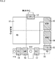
- FIG. 2 is a top view showing a layout example of each component of the solid-state imaging device shown in FIG.
- the first memory 13 and the second memory 14 are arranged symmetrically with respect to the condensing center of the PD 11.
- the noise charge generated by the PD 11 due to stray light can be uniformly accumulated in the first memory 13 and the second memory 14, and the noise charge can be accurately obtained from the signal charge on which the noise charge is superimposed in the subsequent stage. Can be removed.
- FIG. 3 shows a cross section of the solid-state imaging device shown in FIG. 1 and the corresponding potential.
- FIG. 3A is a cross-sectional view
- FIG. 3B shows a potential diagram in a state where the solid-state imaging device is completely reset and no electric charge remains anywhere in the circuit.
- the first pixel driving process of the solid-state imaging device shown in FIG. 1 will be described with reference to FIGS.
- the first memory 13 is used for storing signal charges (including noise charges caused by stray light) converted by the PD 11
- the second memory 14 is used for noise charges caused by stray light. Used for accumulating
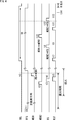
- FIG. 4 shows a timing chart showing driving of each component in the first pixel driving process.
- FIG. 10 is a flowchart for explaining the first pixel driving process.
- the transfer gate 15 is the third time from the timing t6 after the exposure period ends. It is assumed that the timing is t12.
- OFG 12 is opened and unnecessary charge component N0 in the initial state accumulated in PD 11 of all pixels is discharged to Vdd.
- OFG 12 is closed and PD 11 in all pixels is discharged. Are simultaneously started (corresponding to step S1 in FIG. 10).
- the second memory 14 is turned on and off to temporarily be in a high potential state, and the unnecessary charge component N0 in the initial state stored in the first memory 13 is second. It moves to the memory 14 and the first memory 13 is reset.
- the transfer gate 15 is opened and the RST transistor 17 is turned on at timing t3, the transfer gate 15 is closed at timing t4, and the RST transistor 17 is turned off at timing t5.
- the unnecessary charge component N0 in the second memory 14 is reset (corresponding to step S2 in FIG. 10).
- the first memory 13 is turned on and off to temporarily be in a high potential state, and the signal charge S0 accumulated in the PD 11 during the exposure period is the first memory 13. Is completely transferred (corresponding to step S3 in FIG. 10). Thereafter, the noise charges N1 generated by the PD 11 due to stray light are uniformly accumulated in the first memory 13 and the second memory 14 (corresponding to step S4 in FIG. 10).
- the RST transistor 17 is turned on and the FD 16 is reset, and the level (reset level) of the FD 16 at this time is acquired as the first value (corresponding to step S5 in FIG. 10).
- the transfer gate 15 is opened, and the noise charge N1 stored in the second memory 14 is transferred to the FD 16, and at timing t9, the transfer gate 15 is closed, and the FD 16 at this time
- the level (PLS level) is acquired as the second value (corresponding to step S6 in FIG. 10).
- the second memory 14 is turned on and off to temporarily be in a high potential state, and the signal charge S ⁇ b> 0 + noise charge N ⁇ b> 1 accumulated in the first memory 13 moves to the second memory 14.
- the first memory 13 is reset (corresponding to step S7 in FIG. 10).
- the RST transistor 17 is turned on and the FD 16 is reset, and the level (reset level) of the FD 16 at this time is acquired as the third value (corresponding to step S8 in FIG. 10).
- the transfer gate 15 is opened, the signal charge S0 + noise charge N1 transferred to the second memory 14 is transferred to the FD 16, and at timing t13, the transfer gate 15 is closed.
- FD16 level (signal + PLS level) is acquired as the fourth value (corresponding to step S9 in FIG. 10).
- a pixel signal value corresponding to the signal charge S0 from which the noise charge N1 has been removed is calculated according to the following equation (1) in the subsequent stage (corresponding to step S10 in FIG. 10).
- Pixel signal value (fourth value ⁇ third value) ⁇ (second value ⁇ first value) (1)
- the second pixel driving process of the solid-state imaging device shown in FIG. 1 will be described with reference to FIGS.
- the first memory 13 is used for the purpose of accumulating noise charges caused by stray light
- the second memory 14 is a signal charge converted by the PD 11 (including noise charges caused by stray light). Used for accumulating
- FIG. 11 is a timing chart showing driving of each component in the second pixel driving process.
- FIG. 10 is a flowchart corresponding to the timing chart of FIG.
- the transfer gate 15 is the third time from the timing t5 after the exposure period ends. It is assumed that the timing until the timing t11 is opened.
- OFG 12 is opened and unnecessary charge component N0 in the initial state accumulated in PD 11 of all pixels is discharged to Vdd.
- OFG 12 is closed and PD 11 in all pixels is discharged. Are simultaneously started.
- the second memory 14 is turned on and off to temporarily be in a high potential state, and the unnecessary charge component N0 in the initial state stored in the first memory 13 is second. It moves to the memory 14 and the first memory 13 is reset.
- the first memory 13 is turned on and off to temporarily be in a high potential state, and the signal charge S0 accumulated in the PD 11 during the exposure period is completely transferred to the first memory 13.
- the transfer gate 15 is opened, the RST transistor 17 is turned on, and the unnecessary charge component N0 of the second memory 14 is transferred to the FD 16 and discharged to Vdd.
- the second memory 14 is turned on and off to temporarily be in a high potential state, and the signal charge S0 stored in the first memory 13 is moved to the second memory 14.
- the transfer gate 15 is closed.
- the RST transistor 17 is turned off. Thereafter, the noise charges N1 generated by the PD 11 due to stray light are uniformly accumulated in the first memory 13 and the second memory 14.
- the RST transistor 17 is turned on and the FD 16 is reset, and the level (reset level) of the FD 16 at this time is acquired as the first value.
- the transfer gate 15 is opened, and the signal charge S0 + noise charge N1 accumulated in the second memory 14 is transferred to the FD 16, and at timing t8, the transfer gate 15 is closed.
- the level of FD16 (signal + PLS level) is acquired as the second value.
- the second memory 14 is turned on and off to temporarily be in a high potential state, and the noise charge N1 accumulated in the first memory 13 is moved to the second memory 14 to be the first.
- the memory 13 is reset.
- the RST transistor 17 is turned on and the FD 16 is reset, and the level (reset level) of the FD 16 at this time is acquired as the third value.
- the transfer gate 15 is opened, and the noise charge N1 transferred to the second memory 14 is transferred to the FD 16.
- the transfer gate 15 is closed, and the FD 16 at this time
- the level (PLS level) is acquired as the fourth value.
- Pixel signal value (second value ⁇ first value) ⁇ (fourth value ⁇ third value) (2)
- the first pixel driving process and the second pixel driving process described above may be executed by adopting either one, or may be executed alternately at a predetermined cycle (for example, every frame or every predetermined time). It may be.
- the noise charges N0 accumulated in the first memory 13 and the second memory 14 coincide with each other due to the influence of the optical incident angle. Even if it is not, it is possible to obtain the ratio of noise charges accumulated in the first memory 13 and the second memory 14 for each angle of view area by arithmetic processing or the like. Compared to the case, it is possible to remove noise components with higher accuracy.
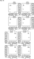
- FIG. 17 is a top view showing a first arrangement example of pixels in the solid-state imaging device. Note that Gr, R, B, and Gb in the middle indicate colors (wavelengths) at which each pixel has sensitivity.
- FIG. 18 is a top view showing a second arrangement example of pixels in the solid-state imaging device.
- the direction of 2 ⁇ 2 pixels adjacent in the horizontal direction forming the Bayer array is inverted vertically for each column.
- the relative positional relationship between the PD 11 and the first memory 13 and the second memory 14 is upside down in the adjacent pixels of the same color in the horizontal direction. Therefore, in the second arrangement example, the first pixel driving process and the second pixel driving process can be performed only by adopting and executing either the first pixel driving process or the second pixel driving process described above. It is possible to obtain the same effect as in the case where the process is executed alternately at a predetermined cycle.
- FIG. 19 is a top view illustrating a third arrangement example of pixels in the solid-state imaging device.
- the orientation of 2 ⁇ 2 pixels adjacent in the vertical direction forming a Bayer array is reversed left and right for each row.
- the relative positional relationship between the PD 11 and the first memory 13 and the second memory 14 is reversed in the vertical direction in the same color adjacent pixels. Therefore, in the third arrangement example, the first pixel driving process and the second pixel driving process can be performed only by adopting and executing either the first pixel driving process or the second pixel driving process described above. It is possible to obtain the same effect as in the case where the process is executed alternately at a predetermined cycle.
- FIG. 20 is a top view illustrating a first modification of the solid-state imaging device illustrated in FIGS. 1 and 2.
- the FD 16 the RST transistor 17, the AMP transistor 18.
- the SEL transistor 19 is shared.
- the element area can be reduced without changing the number of pixels of the solid-state imaging element.
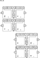
- FIG. 21 is a top view showing an arrangement example (fourth arrangement example) when the first modification example shown in FIG. 20 is arranged on the solid-state imaging device.
- the fourth arrangement example 2 ⁇ 2 pixel units adjacent in the horizontal direction are arranged shifted by one pixel in the column direction.
- the first pixel driving process and the second pixel driving process can be performed only by adopting and executing either the first pixel driving process or the second pixel driving process described above. It is possible to obtain the same effect as in the case where the process is executed alternately at a predetermined cycle.
- FIG. 22 is a top view showing a second modification of the solid-state imaging device shown in FIGS. 1 and 2.
- the FD 16 the RST transistor 17, the AMP transistor 18.
- the SEL transistor 19 is shared.
- the element area can be further reduced as compared with the first modification without changing the number of pixels of the solid-state imaging device.
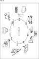
- FIG. 23 shows a usage example of the solid-state imaging device according to the present embodiment.
- the solid-state imaging device described above can be used in various cases for sensing light such as visible light, infrared light, ultraviolet light, and X-ray as follows.
- Devices for taking images for viewing such as digital cameras and mobile devices with camera functions
- Devices used for traffic such as in-vehicle sensors that capture the back, surroundings, and interiors of vehicles, surveillance cameras that monitor traveling vehicles and roads, and ranging sensors that measure distances between vehicles, etc.
- Equipment used for home appliances such as TVs, refrigerators, air conditioners, etc. to take pictures and operate the equipment according to the gestures
- Equipment used for medical and health care ⁇
- Security equipment such as security surveillance cameras and personal authentication cameras
- Skin measuring instrument for photographing skin and scalp photography Such as a microscope to do beauty Equipment used for sports such as action cameras and wearable cameras for sports applications etc.
- Equipment used for agriculture such as cameras for monitoring the condition of fields and crops
- This indication can also take the following composition.
- a photoelectric conversion unit that generates charges in response to incident light;
- An accumulator for accumulating the signal charge generated by the photoelectric converter and converting it into an electrical signal;
- a first holding unit and a second holding unit which are arranged in series between the photoelectric conversion unit and the storage unit and temporarily hold the signal charge generated by the photoelectric conversion unit and then transfer the signal charge to the storage unit;
- Prepared, One of the first and second holding units is used to hold an input noise charge while holding the signal charge generated by the photoelectric conversion unit,
- maintenance part is used for the use which hold
- the solid-state imaging device further including an OFG that resets the photoelectric conversion unit by discharging charges remaining in the photoelectric conversion unit.
- maintenance part is comprised from CCD.
- the solid-state image sensor as described in said (1) or (2).
- the solid-state imaging device according to any one of (1) to (4), wherein the first and second holding units are arranged at positions symmetrical with respect to a condensing center of the photoelectric conversion unit.
- An electric signal level based on the signal charge in a state where the noise charge is superimposed and held in one of the first and second holding units is held in the other of the first and second holding units.
- a first pixel driving process to be acquired after an electric signal level based on the noise charge An electric signal level based on the signal charge in a state where the noise charge is superimposed and held in one of the first and second holding units is held in the other of the first and second holding units.
- a first pixel driving process to be acquired after an electric signal level based on the noise charge Alternatively, an electric signal level based on the signal charge in a state where the noise charge is superimposed and held in one of the first and second holding units is applied to the other of the first and second holding units.
- the solid-state imaging device according to any one of (1) to (12), wherein the storage unit is shared by a plurality of pixels.
- the solid-state image sensor is, for each pixel, A photoelectric conversion unit that generates charges in response to incident light; An accumulator for accumulating the signal charge generated by the photoelectric converter and converting it into an electrical signal; A first holding unit and a second holding unit which are arranged in series between the photoelectric conversion unit and the storage unit and temporarily hold the signal charge generated by the photoelectric conversion unit and then transfer the signal charge to the storage unit; Prepared, One of the first and second holding units is used to hold an input noise charge while holding the signal charge generated by the photoelectric conversion unit, The electronic device used for the purpose of holding the input noise charge while the other of the first and second holding units does not hold the signal charge generated by the photoelectric conversion unit.
Landscapes
- Engineering & Computer Science (AREA)
- Multimedia (AREA)
- Signal Processing (AREA)
- Solid State Image Pick-Up Elements (AREA)
- Transforming Light Signals Into Electric Signals (AREA)
Abstract
本開示は、迷光に起因するノイズ成分を適切に除去できるように、該ノイズ成分を正確に抽出することができるようにする固体撮像素子、および電子装置に関する。 本開示の一側面である固体撮像素子は、光電変換部によって発生された信号電荷を蓄積して電気信号に変換する蓄積部と、前記光電変換部と前記蓄積部の間に直列に配置され、前記光電変換部によって発生された前記信号電荷を一時的に保持した後に前記蓄積部まで転送する第1および第2の保持部とを備え、前記第1および第2の保持部の一方は、前記光電変換部により発生された前記信号電荷を保持している状態で、入力されるノイズ電荷も保持する用途に使用され、前記第1および第2の保持部の他方は、前記光電変換部により発生された前記信号電荷を保持していない状態で、入力されるノイズ電荷を保持する用途に使用される。本開示は、例えば、裏面照射型CMOSイメージセンサに適用できる。
Description
本開示は、固体撮像素子、および電子装置に関し、特に、迷光に起因してノイズ成分を除去できるようにした固体撮像素子、および電子装置に関する。
従来、CMOSイメージセンサ(以下、CISと略称する)は各画素の露光タイミングが行毎にずれてしまうローリングシャッタ方式であった。ローリングシャッタ方式の場合、高速に移動する被写体を撮像するとフォーカルプレーン歪が生じてしまうので、全画素の露光タイミングを統一することができるグローバルシャッタ方式が開発されている。
グローバルシャッタ方式を採用したCISは、入射光に応じて光電変換を行うPD(フォトダイオード)からの信号電荷を電荷保持部としてのFD(フローティングデュフージョン)に転送し、FDが次の読み出し期間まで転送された信号電荷を保持する構造を有する。
ただし、FDが信号電荷を保持している期間にPDに対して強い光が入射すると、入射光量に応じた迷光(PLS)によって発生した電荷(以下、ノイズ電荷とも称する)がFDに混入してしまい、保持されている信号電荷にノイズ成分として重畳されてしまう。これにより、画素信号にはノイズが含まれていることになるので、得られる画像は画質が著しく劣化したものとなる。
そこで、従来、FDから読み出される電荷(信号電荷+ノイズ電荷)からノイズ電荷を減算するための仕組みとして、各画素回路にノイズ電荷用の容量を設けた発明が提案されている(例えば、特許文献1参照)。
特許文献1に記載の発明の場合、FDには、PDで入射光から変換された信号電荷が転送トランジスタおよび第1のスイッチを介して転送、保持されるようにされており、同様に、ノイズ電荷用の容量には、PDで迷光により生じたノイズ電荷が転送トランジスタおよび第2のスイッチを介して転送、保持されるようにされている。
このように、FDとノイズ電荷用の容量にはそれぞれスイッチが必要となるで、画素回路の素子面積がそれらの分だけ増大してしまうことになる。またスイッチを設けたことにより、それらをオン、オフする際に生じるKTCノイズが電荷に重畳されてしまうことになる。
さらに、PDの配置に対するFDとノイズ電荷用の容量の配置については言及されていないので、FDとノイズ電荷用の容量に同量のノイズ電荷が保持されるとは限らず、迷光に起因するノイズ成分を適切に除去できないことも起こり得る。
本開示はこのような状況に鑑みてなされたものであり、グローバルシャッタ方式の固体撮像素子において生じ得る迷光に起因するノイズ成分を適切に除去できるように該ノイズ成分を正確に抽出するものである。
本開示の一側面である固体撮像素子は、全画素の露光期間が統一されるグローバルシャッタ方式の固体撮像素子において、画素毎に、入射光に応じて電荷を発生する光電変換部と、前記光電変換部によって発生された前記信号電荷を蓄積して電気信号に変換する蓄積部と、前記光電変換部と前記蓄積部の間に直列に配置され、前記光電変換部によって発生された前記信号電荷を一時的に保持した後に前記蓄積部まで転送する第1および第2の保持部とを備え、前記第1および第2の保持部の一方は、前記光電変換部により発生された前記信号電荷を保持している状態で、入力されるノイズ電荷も保持する用途に使用され、前記第1および第2の保持部の他方は、前記光電変換部により発生された前記信号電荷を保持していない状態で、入力されるノイズ電荷を保持する用途に使用される。
本開示の一側面である固体撮像素子は、前記光電変換部に残った電荷を排出することにより前記光電変換部をリセットするOFGをさらに備えることができる。
前記第1および第2の保持部は、CCDから構成することができる。
前記第1および第2の保持部には、迷光に起因して前記光電変換部にて生じた等価の前記ノイズ電荷が入力されるようにすることができる。
前記第1および第2の保持部は、前記光電変換部の集光中心に対して対称な位置に配置することができる。
本開示の一側面である固体撮像素子は、前記第1および第2の保持部の一方に保持されている、前記ノイズ電荷が重畳された状態の前記信号電荷に基づく電気信号レベルを、前記第1および第2の保持部の他方に保持されている前記ノイズ電荷に基づく電気信号レベルよりも後に取得する第1の画素駆動処理と、前記第1および第2の保持部の一方に保持されている、前記ノイズ電荷が重畳された状態の前記信号電荷に基づく電気信号レベルを、前記第1および第2の保持部の他方に保持されている前記ノイズ電荷に基づく電気信号レベルよりも先に取得する第2の画素駆動処理とを実行することができる。
前記第1の画素駆動処理と前記第2の画素駆動処理とは、フレーム毎に交互に実行することができる。
前記第1の画素駆動処理と前記第2の画素駆動処理とは、所定の時間毎に交互に実行することができる。
同じ行または同じ列の同色の画素は、前記光電変換部の集光中心に対して対称な位置に配置されている前記第1および第2の保持部の位置関係が入れ替わっているようにすることができる。
本開示の一側面である固体撮像素子は、前記第1および第2の保持部の一方に保持されている、前記ノイズ電荷が重畳された状態の前記信号電荷に基づく電気信号レベルを、前記第1および第2の保持部の他方に保持されている前記ノイズ電荷に基づく電気信号レベルよりも後に取得する第1の画素駆動処理、または、前記第1および第2の保持部の一方に保持されている、前記ノイズ電荷が重畳された状態の前記信号電荷に基づく電気信号レベルを、前記第1および第2の保持部の他方に保持されている前記ノイズ電荷に基づく電気信号レベルよりも先に取得する第2の画素駆動処理を実行することができる。
本開示の一側面である固体撮像素子は、裏面照射型とすることができる。
本開示の一側面である固体撮像素子は、表面照射型とすることができる。
前記蓄積部は、複数の画素によって共有することができる。
本開示の一側面である電子装置は、全画素の露光期間が統一されるグローバルシャッタ方式の固体撮像素子を搭載した電子装置において、前記固体撮像素子は、画素毎に、入射光に応じて電荷を発生する光電変換部と、前記光電変換部によって発生された前記信号電荷を蓄積して電気信号に変換する蓄積部と、前記光電変換部と前記蓄積部の間に直列に配置され、前記光電変換部によって発生された前記信号電荷を一時的に保持した後に前記蓄積部まで転送する第1および第2の保持部とを備え、前記第1および第2の保持部の一方は、前記光電変換部により発生された前記信号電荷を保持している状態で、入力されるノイズ電荷も保持する用途に使用され、前記第1および第2の保持部の他方は、前記光電変換部により発生された前記信号電荷を保持していない状態で、入力されるノイズ電荷を保持する用途に使用される。
本開示の一側面においては、光電変換部と蓄積部の間に直列に配置され、光電変換部によって発生された信号電荷を一時的に保持した後に前記蓄積部まで転送する第1および第2の保持部の一方により、前記光電変換部により発生された前記信号電荷を保持している状態で、入力されるノイズ電荷も保持され、前記第1および第2の保持部の他方は、前記光電変換部により発生された前記信号電荷が保持される。
本開示の一側面によれば、迷光に起因するノイズ成分を適切に除去できるように、該ノイズ成分を正確に抽出できる。
以下、本開示を実施するための最良の形態(以下、実施の形態と称する)について、図面を参照しながら詳細に説明する。
<本実施の形態である固体撮像素子の構成例>
図1は、本実施の形態である固体撮像素子の1画素分の構成例を示す等価回路図である。なお、本実施の形態である固体撮像素子は、裏面照射型または表面照射型のどちらにも適用できる。
図1は、本実施の形態である固体撮像素子の1画素分の構成例を示す等価回路図である。なお、本実施の形態である固体撮像素子は、裏面照射型または表面照射型のどちらにも適用できる。
この固体撮像素子は、PD(フォトダイオード)11、OFG(オーバフローゲート)12、第1メモリ(MEM1)13、第2メモリ(MEM2)14、転送ゲート(TG)15、FD(フローティングデュフージョン)16、RSTトランジスタ17、AMPトランジスタ18、およびSELトランジスタ19を有する。
PD11は、光電変換素子であり、入射光を受光して、その入射光に対応する電荷を蓄積することによって光電変換を行う。PD11は、そのアノードがGNDに接続され(接地され)、そのカソードが、第1メモリ13および第2メモリ14を介して転送ゲート15に接続されている。OFG12は、初期状態のPD11に残っている電荷をオーバフロードレインに排出させる際に駆動される。
第1メモリ13および第2メモリ14の一方は、PD11にて変換された信号電荷を保持している状態で、迷光に起因するノイズ電荷も保持する用途に使用される。また、第1メモリ13および第2メモリ14の他方は、PD11にて変換された信号電荷を保持していない状態で、迷光に起因するノイズ電荷を保持する用途に使用される。
第1メモリ13および第2メモリ14には、例えば埋め込みチャネルのCCD(Charge Coupled Device)を用いることができる。第1メモリ13および第2メモリ14にCCDを用いることにより、第1メモリ13と第2メモリ14それぞれに蓄積される電荷を後段に完全転送することができる。
転送ゲート15は、PD11にて変換された信号電荷をFD16に転送する際に駆動される。FD16は、転送ゲート15とRSTトランジスタ17との接続点に形成される領域であり、FD16において、そこに供給された電荷が電圧に変換される。
RSTトランジスタ17は、FD16に蓄積された電荷(電圧(電位))をリセットする際に駆動される。
AMPトランジスタ18は、FD16の電圧をバッファリングするために設けられる。SELトランジスタ19は、AMPトランジスタ18にてバッファリングされた電位を垂直信号線20に出力させる画素を選択するために駆動される。
なお、OFG12、転送ゲート15、RSTトランジスタ17、AMPトランジスタ18、およびSELトランジスタ19には、例えばMOSトランジスタを用いることができる。
図2は、図1に示された固体撮像素子の各構成要素のレイアウト例を示す上面図である。
固体撮像素子の構成要素のうち、特に、第1メモリ13と第2メモリ14については、PD11の集光中心に対して対称に配置される。これにより、迷光に起因してPD11が生じさせるノイズ電荷を第1メモリ13と第2メモリ14に均等に蓄積させることができ、後段においてノイズ電荷が重畳されている信号電荷から正確にノイズ電荷を除去することができる。
図3は、図1に示された固体撮像素子の断面とそれに対応するポテンシャルを示している。同図Aが断面図であり、図3のBは固体撮像素子が完全にリセットされて、回路内のどこにも電荷が残っていない状態のポテンシャルダイアグラムを示している。
<本開示の実施の形態である固体撮像素子の画素駆動処理>
次に、図1に示された固体撮像素子の第1の画素駆動処理について、図4乃至図10を参照して説明する。第1の画素駆動処理では、第1メモリ13をPD11にて変換される信号電荷(迷光に起因するノイズ電荷を含む)を蓄積する用途に使用し、第2メモリ14を迷光に起因するノイズ電荷を蓄積する用途に使用する。
次に、図1に示された固体撮像素子の第1の画素駆動処理について、図4乃至図10を参照して説明する。第1の画素駆動処理では、第1メモリ13をPD11にて変換される信号電荷(迷光に起因するノイズ電荷を含む)を蓄積する用途に使用し、第2メモリ14を迷光に起因するノイズ電荷を蓄積する用途に使用する。
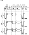
図4は、第1の画素駆動処理における各構成要素の駆動を示すタイミングチャートを示している。
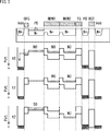
図5乃至図9は、第1の画素駆動処理におけるポテンシャルダイアグラムの推移を示している。図10は、第1の画素駆動処理を説明するフローチャートである。
ただし前提として、迷光に起因してPD11が生じさせるノイズ電荷N1が第1メモリ13と第2メモリ14に均等に蓄積される期間は、露光期間終了後のタイミングt6から転送ゲート15が3回目に開かれるタイミングt12までと仮定する。
始めに、タイミングt0にて、OFG12が開けられて全画素のPD11に蓄積されている初期状態の不要な電荷成分N0がVddに排出され、タイミングt1にて、OFG12が閉じられて全画素におけるPD11の露光が同時に開始される(図10のステップS1に相当)。
V_BLK期間には、タイミングt2にて、第2メモリ14がオン、オフされて一時的に高ポテンシャルの状態とされ、第1メモリ13に蓄積されている初期状態の不要な電荷成分N0が第2メモリ14に移動されて第1メモリ13がリセットされる。次に、タイミングt3にて、転送ゲート15が開かれるとともにRSTトランジスタ17がオンとされ、タイミングt4にて、転送ゲート15が閉じられ、タイミングt5にて、RSTトランジスタ17がオフとされることにより、第2メモリ14の不要な電荷成分N0がリセットされる(図10のステップS2に相当)。
次に、露光期間の終わりとなるタイミングt6にて、第1メモリ13がオン、オフされて一時的に高ポテンシャルの状態とされ、露光期間にPD11に蓄積された信号電荷S0が第1メモリ13に完全転送される(図10のステップS3に相当)。この後、第1メモリ13と第2メモリ14には、迷光に起因してPD11が生じさせるノイズ電荷N1が均等に蓄積されることになる(図10のステップS4に相当)。
タイミングt7にて、RSTトランジスタ17がオンとされてFD16がリセットされ、このときのFD16のレベル(リセットレベル)が第1の値として取得される(図10のステップS5に相当)。
続いてタイミングt8にて、転送ゲート15が開かれて、第2メモリ14に蓄積されたノイズ電荷N1がFD16に転送され、タイミングt9にて、転送ゲート15が閉じられて、このときのFD16のレベル(PLSレベル)が第2の値として取得される(図10のステップS6に相当)。
次に、タイミングt10にて、第2メモリ14がオン、オフされて一時的に高ポテンシャルの状態とされ、第1メモリ13に蓄積されている信号電荷S0+ノイズ電荷N1が第2メモリ14に移動されて第1メモリ13がリセットされる(図10のステップS7に相当)。
タイミングt11にて、RSTトランジスタ17がオンとされてFD16がリセットされ、このときのFD16のレベル(リセットレベル)が第3の値として取得される(図10のステップS8に相当)。
続いてタイミングt12にて、転送ゲート15が開かれて、第2メモリ14に転送された信号電荷S0+ノイズ電荷N1がFD16に転送され、タイミングt13にて、転送ゲート15が閉じられて、このときのFD16のレベル(信号+PLSレベル)が第4の値として取得される(図10のステップS9に相当)。
この後、タイミングt14にて、後段において次式(1)に従い、ノイズ電荷N1を除去した信号電荷S0に対応する画素信号値が算出される(図10のステップS10に相当)。
画素信号値=(第4の値-第3の値)-(第2の値-第1の値) ・・・(1)
画素信号値=(第4の値-第3の値)-(第2の値-第1の値) ・・・(1)
なお、上記した演算を実行するためには1H分のメモリを確保する必要がある。
次に、図1に示された固体撮像素子の第2の画素駆動処理について、図11乃至図16を参照して説明する。第2の画素駆動処理では、第1メモリ13を迷光に起因するノイズ電荷を蓄積する用途に使用し、第2メモリ14をPD11にて変換される信号電荷(迷光に起因するノイズ電荷を含む)を蓄積する用途に使用する。
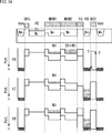
図11は、第2の画素駆動処理における各構成要素の駆動を示すタイミングチャートを示している。
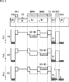
図12乃至図16は、図4の各タイミングt0乃至t14におけるポテンシャルダイアグラムの推移を示している。図10は、図4のタイミングチャートに対応するフローチャートである。
ただし、前提として、迷光に起因してPD11が生じさせるノイズ電荷N1が第1メモリ13と第2メモリ14に均等に蓄積される期間は、露光期間終了後のタイミングt5から転送ゲート15が3回目に開かれるタイミングt11までと仮定する。
始めに、タイミングt0にて、OFG12が開けられて全画素のPD11に蓄積されている初期状態の不要な電荷成分N0がVddに排出され、タイミングt1にて、OFG12が閉じられて全画素におけるPD11の露光が同時に開始される。
V_BLK期間には、タイミングt2にて、第2メモリ14がオン、オフされて一時的に高ポテンシャルの状態とされ、第1メモリ13に蓄積されている初期状態の不要な電荷成分N0が第2メモリ14に移動されて第1メモリ13がリセットされる。次に、タイミングt3にて、第1メモリ13がオン、オフされて一時的に高ポテンシャルの状態とされて、露光期間にPD11に蓄積された信号電荷S0が第1メモリ13に完全転送されるとともに、転送ゲート15が開かれ、RSTトランジスタ17がオンとされて第2メモリ14の不要な電荷成分N0がFD16に転送されてVddに排出される。
次に、タイミングt4にて、第2メモリ14がオン、オフされて一時的に高ポテンシャルの状態とされ、第1メモリ13に蓄積されている信号電荷S0が第2メモリ14に移動されるとともに、転送ゲート15が閉じられる。続いて、露光期間の終わりとなるタイミングt5にて、RSTトランジスタ17がオフとされる。この後、第1メモリ13と第2メモリ14には、迷光に起因してPD11が生じさせるノイズ電荷N1が均等に蓄積されることになる。
タイミングt6にて、RSTトランジスタ17がオンとされてFD16がリセットされ、このときのFD16のレベル(リセットレベル)が第1の値として取得される。
続いてタイミングt7にて、転送ゲート15が開かれて、第2メモリ14に蓄積された信号電荷S0+ノイズ電荷N1がFD16に転送され、タイミングt8にて、転送ゲート15が閉じられて、このときのFD16のレベル(信号+PLSレベル)が第2の値として取得される。
次に、タイミングt9にて、第2メモリ14がオン、オフされて一時的に高ポテンシャルの状態とされ、第1メモリ13に蓄積されたノイズ電荷N1が第2メモリ14に移動されて第1メモリ13がリセットされる。
タイミングt10にて、RSTトランジスタ17がオンとされてFD16がリセットされ、このときのFD16のレベル(リセットレベル)が第3の値として取得される。
続いてタイミングt11にて、転送ゲート15が開かれて、第2メモリ14に転送されたノイズ電荷N1がFD16に転送され、タイミングt12にて、転送ゲート15が閉じられて、このときのFD16のレベル(PLSレベル)が第4の値として取得される。
この後、タイミングt13にて、後段において次式(2)に従い、ノイズ電荷N1を除去した信号電荷S0に対応する画素信号値が算出される。
画素信号値=(第2の値-第1の値)-(第4の値-第3の値) ・・・(2)
画素信号値=(第2の値-第1の値)-(第4の値-第3の値) ・・・(2)
なお、上記した演算を実行するためには1H分のメモリを確保する必要がある。
上述した第1の画素駆動処理と第2の画素駆動処理は、どちらか一方を採用して実行すればよいし、所定の周期(例えば、フレーム毎または所定の時間毎)で交互に実行するようにしてもよい。
第1の画素駆動処理と第2の画素駆動処理を交互に実行した場合、例えば、光学的な入射角の影響で、第1メモリ13と第2メモリ14に蓄積されるノイズ電荷N0が一致していなくても、演算処理等により、画角エリア毎にノイズ電荷が第1メモリ13と第2メモリ14に蓄積される比率を求める事が可能になるので、どちらか一方を採用して実行する場合に比較して、より精度が高いノイズ成分除去が可能になる。
<固体撮像素子における画素の配置例>
次に、本開示の実施の形態である固体撮像素子における画素の配置例について説明する。
次に、本開示の実施の形態である固体撮像素子における画素の配置例について説明する。
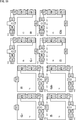
図17は、固体撮像素子における画素の第1の配置例を示す上面図である。なお、中におけるGr,R,B,Gbは、それぞれの画素が感度を有する色(波長)を示している。
第1の配置例は、画素の色に着目した場合、ベイヤ配列を成しており、全ての画素の構成要素のレイアウトは共通とされ、各画素の向きも統一されたものである。
図18は、固体撮像素子における画素の第2の配置例を示す上面図である。第2の配置例は、ベイヤ配列をなす横方向に隣接する2×2画素の向きが列毎に上下反転されたものである。
第2の配置例によれば、横方向の同色隣接画素で、PD11と第1メモリ13および第2メモリ14との相対位置関係が上下逆になる。したがって、第2の配置例では、上述した第1の画素駆動処理または第2の画素駆動処理のどちらか一方を採用して実行するだけで、第1の画素駆動処理と第2の画素駆動処理を所定の周期で交互に実行する場合と同様の効果を得ることができる。
図19は、固体撮像素子における画素の第3の配置例を示す上面図である。第3の配置例は、ベイヤ配列を成す縦方向に隣接する2×2画素の向きが行毎に左右反転されたものである。
第3の配置例によれば、縦方向の同色隣接画素で、PD11と第1メモリ13および第2メモリ14との相対位置関係が左右逆になる。したがって、第3の配置例では、上述した第1の画素駆動処理または第2の画素駆動処理のどちらか一方を採用して実行するだけで、第1の画素駆動処理と第2の画素駆動処理を所定の周期で交互に実行する場合と同様の効果を得ることができる。
<固体撮像素子の変形例>
図20は、図1および図2に示された固体撮像素子の第1の変形例を示す上面図である。第1の変形例は、縦方向に隣接する2画素によりFD16、RSTトランジスタ17、AMPトランジスタ18.およびSELトランジスタ19を共有する構成を有する。
図20は、図1および図2に示された固体撮像素子の第1の変形例を示す上面図である。第1の変形例は、縦方向に隣接する2画素によりFD16、RSTトランジスタ17、AMPトランジスタ18.およびSELトランジスタ19を共有する構成を有する。
第1の変形例によれば、固体撮像素子の画素数を変えることなく素子面積を縮小することができる。
図21は、図20に示された第1の変形例を固体撮像素子上に配置する場合の配置例(第4の配置例)を示す上面図である。第4の配置例は、横方向に隣接する2×2画素単位が列方向に1画素分ずつずらして配置されたものである。
第4の配置例によれば、上述した第1の画素駆動処理または第2の画素駆動処理のどちらか一方を採用して実行するだけで、第1の画素駆動処理と第2の画素駆動処理を所定の周期で交互に実行する場合と同様の効果を得ることができる。
図22は、図1および図2に示された固体撮像素子の第2の変形例を示す上面図である。第2の変形例は、2×2画素によりFD16、RSTトランジスタ17、AMPトランジスタ18.およびSELトランジスタ19を共有する構成を有する。
第2の変形例によれば、固体撮像素子の画素数を変えることなく、素子面積を第1の変形例よりもさらに縮小することができる。
<固体撮像素子の使用例>
図23は、本実施の形態である固体撮像素子の使用例を示している。
図23は、本実施の形態である固体撮像素子の使用例を示している。
上述した固体撮像素子は、例えば、以下のように、可視光や、赤外光、紫外光、X線等の光をセンシングする様々なケースに使用することができる。
・デジタルカメラや、カメラ機能付きの携帯機器等の、鑑賞の用に供される画像を撮影する装置
・自動停止等の安全運転や、運転者の状態の認識等のために、自動車の前方や後方、周囲、車内等を撮影する車載用センサ、走行車両や道路を監視する監視カメラ、車両間等の測距を行う測距センサ等の、交通の用に供される装置
・ユーザのジェスチャを撮影して、そのジェスチャに従った機器操作を行うために、TVや、冷蔵庫、エアーコンディショナ等の家電に供される装置
・内視鏡や、赤外光の受光による血管撮影を行う装置等の、医療やヘルスケアの用に供される装置
・防犯用途の監視カメラや、人物認証用途のカメラ等の、セキュリティの用に供される装置
・肌を撮影する肌測定器や、頭皮を撮影するマイクロスコープ等の、美容の用に供される装置
・スポーツ用途等向けのアクションカメラやウェアラブルカメラ等の、スポーツの用に供される装置
・畑や作物の状態を監視するためのカメラ等の、農業の用に供される装置
・自動停止等の安全運転や、運転者の状態の認識等のために、自動車の前方や後方、周囲、車内等を撮影する車載用センサ、走行車両や道路を監視する監視カメラ、車両間等の測距を行う測距センサ等の、交通の用に供される装置
・ユーザのジェスチャを撮影して、そのジェスチャに従った機器操作を行うために、TVや、冷蔵庫、エアーコンディショナ等の家電に供される装置
・内視鏡や、赤外光の受光による血管撮影を行う装置等の、医療やヘルスケアの用に供される装置
・防犯用途の監視カメラや、人物認証用途のカメラ等の、セキュリティの用に供される装置
・肌を撮影する肌測定器や、頭皮を撮影するマイクロスコープ等の、美容の用に供される装置
・スポーツ用途等向けのアクションカメラやウェアラブルカメラ等の、スポーツの用に供される装置
・畑や作物の状態を監視するためのカメラ等の、農業の用に供される装置
なお、本開示の実施の形態は、上述した実施の形態に限定されるものではなく、本開示の要旨を逸脱しない範囲において種々の変更が可能である。
本開示は以下のような構成も取ることができる。
(1)
全画素の露光期間が統一されるグローバルシャッタ方式の固体撮像素子において、
画素毎に、
入射光に応じて電荷を発生する光電変換部と、
前記光電変換部によって発生された前記信号電荷を蓄積して電気信号に変換する蓄積部と、
前記光電変換部と前記蓄積部の間に直列に配置され、前記光電変換部によって発生された前記信号電荷を一時的に保持した後に前記蓄積部まで転送する第1および第2の保持部とを備え、
前記第1および第2の保持部の一方は、前記光電変換部により発生された前記信号電荷を保持している状態で、入力されるノイズ電荷も保持する用途に使用され、
前記第1および第2の保持部の他方は、前記光電変換部により発生された前記信号電荷を保持していない状態で、入力されるノイズ電荷を保持する用途に使用される
固体撮像素子。
(2)
前記光電変換部に残った電荷を排出することにより前記光電変換部をリセットするOFGを
さらに備える前記(1)に記載の固体撮像素子。
(3)
前記第1および第2の保持部は、CCDから構成される
前記(1)または(2)に記載の固体撮像素子。
(4)
前記第1および第2の保持部には、迷光に起因して前記光電変換部にて生じた等価の前記ノイズ電荷が入力される
前記(1)から(3)のいずれかに記載の固体撮像素子。
(5)
前記第1および第2の保持部は、前記光電変換部の集光中心に対して対称な位置に配置されている
前記(1)から(4)のいずれかに記載の固体撮像素子。
(6)
前記第1および第2の保持部の一方に保持されている、前記ノイズ電荷が重畳された状態の前記信号電荷に基づく電気信号レベルを、前記第1および第2の保持部の他方に保持されている前記ノイズ電荷に基づく電気信号レベルよりも後に取得する第1の画素駆動処理と、
前記第1および第2の保持部の一方に保持されている、前記ノイズ電荷が重畳された状態の前記信号電荷に基づく電気信号レベルを、前記第1および第2の保持部の他方に保持されている前記ノイズ電荷に基づく電気信号レベルよりも先に取得する第2の画素駆動処理とを実行する
前記(1)から(5)のいずれかに記載の固体撮像素子。
(7)
前記第1の画素駆動処理と前記第2の画素駆動処理とをフレーム毎に交互に実行する
前記(6)に記載の固体撮像素子。
(8)
前記第1の画素駆動処理と前記第2の画素駆動処理とを所定の時間毎に交互に実行する
前記(6)に記載の固体撮像素子。
(9)
同じ行または同じ列の同色の画素は、前記光電変換部の集光中心に対して対称な位置に配置されている前記第1および第2の保持部の位置関係が入れ替わっている
前記(1)から(5)のいずれかに記載の固体撮像素子。
(10)
前記第1および第2の保持部の一方に保持されている、前記ノイズ電荷が重畳された状態の前記信号電荷に基づく電気信号レベルを、前記第1および第2の保持部の他方に保持されている前記ノイズ電荷に基づく電気信号レベルよりも後に取得する第1の画素駆動処理、
または、前記第1および第2の保持部の一方に保持されている、前記ノイズ電荷が重畳された状態の前記信号電荷に基づく電気信号レベルを、前記第1および第2の保持部の他方に保持されている前記ノイズ電荷に基づく電気信号レベルよりも先に取得する第2の画素駆動処理を実行する
前記(9)に記載の固体撮像素子。
(11)
裏面照射型である
前記(1)から(10)のいずれかに記載の固体撮像素子。
(12)
表面照射型である
前記(1)から(10)のいずれかに記載の固体撮像素子。
(13)
前記蓄積部は、複数の画素によって共有されている
前記(1)から(12)のいずれかに記載の固体撮像素子。
(14)
全画素の露光期間が統一されるグローバルシャッタ方式の固体撮像素子を搭載した電子装置において、
前記固体撮像素子は、画素毎に、
入射光に応じて電荷を発生する光電変換部と、
前記光電変換部によって発生された前記信号電荷を蓄積して電気信号に変換する蓄積部と、
前記光電変換部と前記蓄積部の間に直列に配置され、前記光電変換部によって発生された前記信号電荷を一時的に保持した後に前記蓄積部まで転送する第1および第2の保持部とを備え、
前記第1および第2の保持部の一方は、前記光電変換部により発生された前記信号電荷を保持している状態で、入力されるノイズ電荷も保持する用途に使用され、
前記第1および第2の保持部の他方は、前記光電変換部により発生された前記信号電荷を保持していない状態で、入力されるノイズ電荷を保持する用途に使用される
電子装置。
(1)
全画素の露光期間が統一されるグローバルシャッタ方式の固体撮像素子において、
画素毎に、
入射光に応じて電荷を発生する光電変換部と、
前記光電変換部によって発生された前記信号電荷を蓄積して電気信号に変換する蓄積部と、
前記光電変換部と前記蓄積部の間に直列に配置され、前記光電変換部によって発生された前記信号電荷を一時的に保持した後に前記蓄積部まで転送する第1および第2の保持部とを備え、
前記第1および第2の保持部の一方は、前記光電変換部により発生された前記信号電荷を保持している状態で、入力されるノイズ電荷も保持する用途に使用され、
前記第1および第2の保持部の他方は、前記光電変換部により発生された前記信号電荷を保持していない状態で、入力されるノイズ電荷を保持する用途に使用される
固体撮像素子。
(2)
前記光電変換部に残った電荷を排出することにより前記光電変換部をリセットするOFGを
さらに備える前記(1)に記載の固体撮像素子。
(3)
前記第1および第2の保持部は、CCDから構成される
前記(1)または(2)に記載の固体撮像素子。
(4)
前記第1および第2の保持部には、迷光に起因して前記光電変換部にて生じた等価の前記ノイズ電荷が入力される
前記(1)から(3)のいずれかに記載の固体撮像素子。
(5)
前記第1および第2の保持部は、前記光電変換部の集光中心に対して対称な位置に配置されている
前記(1)から(4)のいずれかに記載の固体撮像素子。
(6)
前記第1および第2の保持部の一方に保持されている、前記ノイズ電荷が重畳された状態の前記信号電荷に基づく電気信号レベルを、前記第1および第2の保持部の他方に保持されている前記ノイズ電荷に基づく電気信号レベルよりも後に取得する第1の画素駆動処理と、
前記第1および第2の保持部の一方に保持されている、前記ノイズ電荷が重畳された状態の前記信号電荷に基づく電気信号レベルを、前記第1および第2の保持部の他方に保持されている前記ノイズ電荷に基づく電気信号レベルよりも先に取得する第2の画素駆動処理とを実行する
前記(1)から(5)のいずれかに記載の固体撮像素子。
(7)
前記第1の画素駆動処理と前記第2の画素駆動処理とをフレーム毎に交互に実行する
前記(6)に記載の固体撮像素子。
(8)
前記第1の画素駆動処理と前記第2の画素駆動処理とを所定の時間毎に交互に実行する
前記(6)に記載の固体撮像素子。
(9)
同じ行または同じ列の同色の画素は、前記光電変換部の集光中心に対して対称な位置に配置されている前記第1および第2の保持部の位置関係が入れ替わっている
前記(1)から(5)のいずれかに記載の固体撮像素子。
(10)
前記第1および第2の保持部の一方に保持されている、前記ノイズ電荷が重畳された状態の前記信号電荷に基づく電気信号レベルを、前記第1および第2の保持部の他方に保持されている前記ノイズ電荷に基づく電気信号レベルよりも後に取得する第1の画素駆動処理、
または、前記第1および第2の保持部の一方に保持されている、前記ノイズ電荷が重畳された状態の前記信号電荷に基づく電気信号レベルを、前記第1および第2の保持部の他方に保持されている前記ノイズ電荷に基づく電気信号レベルよりも先に取得する第2の画素駆動処理を実行する
前記(9)に記載の固体撮像素子。
(11)
裏面照射型である
前記(1)から(10)のいずれかに記載の固体撮像素子。
(12)
表面照射型である
前記(1)から(10)のいずれかに記載の固体撮像素子。
(13)
前記蓄積部は、複数の画素によって共有されている
前記(1)から(12)のいずれかに記載の固体撮像素子。
(14)
全画素の露光期間が統一されるグローバルシャッタ方式の固体撮像素子を搭載した電子装置において、
前記固体撮像素子は、画素毎に、
入射光に応じて電荷を発生する光電変換部と、
前記光電変換部によって発生された前記信号電荷を蓄積して電気信号に変換する蓄積部と、
前記光電変換部と前記蓄積部の間に直列に配置され、前記光電変換部によって発生された前記信号電荷を一時的に保持した後に前記蓄積部まで転送する第1および第2の保持部とを備え、
前記第1および第2の保持部の一方は、前記光電変換部により発生された前記信号電荷を保持している状態で、入力されるノイズ電荷も保持する用途に使用され、
前記第1および第2の保持部の他方は、前記光電変換部により発生された前記信号電荷を保持していない状態で、入力されるノイズ電荷を保持する用途に使用される
電子装置。
11 PD, 12 OFG, 13 第1メモリ,14 第2メモリ,15 転送ゲート, 16 FD, 17 RSTトランジスタ, 18 AMPトランジスタ, 19 SELトランジスタ, 20VSL
Claims (14)
- 全画素の露光期間が統一されるグローバルシャッタ方式の固体撮像素子において、
画素毎に、
入射光に応じて電荷を発生する光電変換部と、
前記光電変換部によって発生された前記信号電荷を蓄積して電気信号に変換する蓄積部と、
前記光電変換部と前記蓄積部の間に直列に配置され、前記光電変換部によって発生された前記信号電荷を一時的に保持した後に前記蓄積部まで転送する第1および第2の保持部とを備え、
前記第1および第2の保持部の一方は、前記光電変換部により発生された前記信号電荷を保持している状態で、入力されるノイズ電荷も保持する用途に使用され、
前記第1および第2の保持部の他方は、前記光電変換部により発生された前記信号電荷を保持していない状態で、入力されるノイズ電荷を保持する用途に使用される
固体撮像素子。 - 前記光電変換部に残った電荷を排出することにより前記光電変換部をリセットするOFGを
さらに備える請求項1に記載の固体撮像素子。 - 前記第1および第2の保持部は、CCDから構成される
請求項2に記載の固体撮像素子。 - 前記第1および第2の保持部には、迷光に起因して前記光電変換部にて生じた等価の前記ノイズ電荷が入力される
請求項2に記載の固体撮像素子。 - 前記第1および第2の保持部は、前記光電変換部の集光中心に対して対称な位置に配置されている
請求項4に記載の固体撮像素子。 - 前記第1および第2の保持部の一方に保持されている、前記ノイズ電荷が重畳された状態の前記信号電荷に基づく電気信号レベルを、前記第1および第2の保持部の他方に保持されている前記ノイズ電荷に基づく電気信号レベルよりも後に取得する第1の画素駆動処理と、
前記第1および第2の保持部の一方に保持されている、前記ノイズ電荷が重畳された状態の前記信号電荷に基づく電気信号レベルを、前記第1および第2の保持部の他方に保持されている前記ノイズ電荷に基づく電気信号レベルよりも先に取得する第2の画素駆動処理とを実行する
請求項2に記載の固体撮像素子。 - 前記第1の画素駆動処理と前記第2の画素駆動処理とをフレーム毎に交互に実行する
請求項6に記載の固体撮像素子。 - 前記第1の画素駆動処理と前記第2の画素駆動処理とを所定の時間毎に交互に実行する
請求項6に記載の固体撮像素子。 - 同じ行または同じ列の同色の画素は、前記光電変換部の集光中心に対して対称な位置に配置されている前記第1および第2の保持部の位置関係が入れ替わっている
請求項5に記載の固体撮像素子。 - 前記第1および第2の保持部の一方に保持されている、前記ノイズ電荷が重畳された状態の前記信号電荷に基づく電気信号レベルを、前記第1および第2の保持部の他方に保持されている前記ノイズ電荷に基づく電気信号レベルよりも後に取得する第1の画素駆動処理、
または、前記第1および第2の保持部の一方に保持されている、前記ノイズ電荷が重畳された状態の前記信号電荷に基づく電気信号レベルを、前記第1および第2の保持部の他方に保持されている前記ノイズ電荷に基づく電気信号レベルよりも先に取得する第2の画素駆動処理を実行する
請求項9に記載の固体撮像素子。 - 裏面照射型である
請求項2に記載の固体撮像素子。 - 表面照射型である
請求項2に記載の固体撮像素子。 - 前記蓄積部は、複数の画素によって共有されている
請求項2に記載の固体撮像素子。 - 全画素の露光期間が統一されるグローバルシャッタ方式の固体撮像素子を搭載した電子装置において、
前記固体撮像素子は、画素毎に、
入射光に応じて電荷を発生する光電変換部と、
前記光電変換部によって発生された前記信号電荷を蓄積して電気信号に変換する蓄積部と、
前記光電変換部と前記蓄積部の間に直列に配置され、前記光電変換部によって発生された前記信号電荷を一時的に保持した後に前記蓄積部まで転送する第1および第2の保持部とを備え、
前記第1および第2の保持部の一方は、前記光電変換部により発生された前記信号電荷を保持している状態で、入力されるノイズ電荷も保持する用途に使用され、
前記第1および第2の保持部の他方は、前記光電変換部により発生された前記信号電荷を保持していない状態で、入力されるノイズ電荷を保持する用途に使用される
電子装置。
Priority Applications (1)
| Application Number | Priority Date | Filing Date | Title |
|---|---|---|---|
| US15/763,956 US10567687B2 (en) | 2015-10-15 | 2016-09-30 | Solid state imaging device and electronic apparatus for removing a noise component |
Applications Claiming Priority (2)
| Application Number | Priority Date | Filing Date | Title |
|---|---|---|---|
| JP2015203889A JP2017076899A (ja) | 2015-10-15 | 2015-10-15 | 固体撮像素子、および電子装置 |
| JP2015-203889 | 2015-10-15 |
Publications (1)
| Publication Number | Publication Date |
|---|---|
| WO2017065019A1 true WO2017065019A1 (ja) | 2017-04-20 |
Family
ID=58517658
Family Applications (1)
| Application Number | Title | Priority Date | Filing Date |
|---|---|---|---|
| PCT/JP2016/078982 Ceased WO2017065019A1 (ja) | 2015-10-15 | 2016-09-30 | 固体撮像素子、および電子装置 |
Country Status (3)
| Country | Link |
|---|---|
| US (1) | US10567687B2 (ja) |
| JP (1) | JP2017076899A (ja) |
| WO (1) | WO2017065019A1 (ja) |
Cited By (1)
| Publication number | Priority date | Publication date | Assignee | Title |
|---|---|---|---|---|
| CN111670500A (zh) * | 2018-03-22 | 2020-09-15 | 索尼半导体解决方案公司 | 摄像装置和电子设备 |
Families Citing this family (12)
| Publication number | Priority date | Publication date | Assignee | Title |
|---|---|---|---|---|
| JP2020027903A (ja) | 2018-08-15 | 2020-02-20 | ソニーセミコンダクタソリューションズ株式会社 | 固体撮像素子および電子機器 |
| US10834342B2 (en) | 2019-02-01 | 2020-11-10 | Semiconductor Components Industries, Llc | Image sensors with reduced noise |
| US11218653B2 (en) | 2019-07-09 | 2022-01-04 | Semiconductor Components Industries, Llc | Methods and circuitry for improving global shutter efficiency in backside illuminated high dynamic range image sensor pixels |
| CN110501691B (zh) * | 2019-08-13 | 2022-03-08 | Oppo广东移动通信有限公司 | Tof模组的噪声滤除方法、tof模组及装置 |
| KR102885925B1 (ko) * | 2019-11-15 | 2025-11-12 | 삼성전자주식회사 | 픽셀 어레이 및 이를 포함하는 이미지 센서 |
| WO2021171717A1 (ja) * | 2020-02-26 | 2021-09-02 | ソニーセミコンダクタソリューションズ株式会社 | 固体撮像素子、撮像装置および固体撮像素子の制御方法 |
| CN115917725A (zh) * | 2020-10-20 | 2023-04-04 | 索尼半导体解决方案公司 | 固态成像装置 |
| WO2022102404A1 (ja) * | 2020-11-12 | 2022-05-19 | ソニーセミコンダクタソリューションズ株式会社 | 固体撮像素子、電子機器および固体撮像素子の制御方法 |
| JP2022152974A (ja) * | 2021-03-29 | 2022-10-12 | ソニーセミコンダクタソリューションズ株式会社 | 撮像システム及び撮像装置 |
| TW202306210A (zh) * | 2021-06-25 | 2023-02-01 | 日商半導體能源研究所股份有限公司 | 受光器件、受發光裝置 |
| US12527106B2 (en) * | 2022-06-10 | 2026-01-13 | Taiwan Semiconductor Manufacturing Company, Ltd. | Multi-chip image sensor |
| WO2025062832A1 (ja) * | 2023-09-22 | 2025-03-27 | ソニーセミコンダクタソリューションズ株式会社 | 撮像装置、コンパレータおよび撮像方法 |
Citations (3)
| Publication number | Priority date | Publication date | Assignee | Title |
|---|---|---|---|---|
| JP2011188410A (ja) * | 2010-03-11 | 2011-09-22 | Sony Corp | 固体撮像装置、固体撮像装置の駆動方法、及び、電子機器 |
| JP2013211649A (ja) * | 2012-03-30 | 2013-10-10 | Sony Corp | 固体撮像素子および駆動方法、並びに、電子機器 |
| JP2013225734A (ja) * | 2012-04-20 | 2013-10-31 | Sony Corp | 固体撮像装置および電子機器 |
Family Cites Families (6)
| Publication number | Priority date | Publication date | Assignee | Title |
|---|---|---|---|---|
| US7826906B2 (en) * | 2006-11-01 | 2010-11-02 | Intel Corporation | Transducer access point |
| JP5620693B2 (ja) * | 2010-02-26 | 2014-11-05 | パナソニック株式会社 | 固体撮像装置およびその駆動方法、カメラ |
| JP5091964B2 (ja) * | 2010-03-05 | 2012-12-05 | 株式会社東芝 | 固体撮像装置 |
| JP5824942B2 (ja) * | 2011-07-27 | 2015-12-02 | ブラザー工業株式会社 | ディザマトリクス作成装置及びディザマトリクス作成プログラム |
| CN104429056B (zh) * | 2012-08-10 | 2017-11-14 | 株式会社尼康 | 图像处理方法、图像处理装置、摄像装置及图像处理程序 |
| JP2017021425A (ja) * | 2015-07-07 | 2017-01-26 | キヤノン株式会社 | 画像生成装置、画像生成方法、および画像生成プログラム |
-
2015
- 2015-10-15 JP JP2015203889A patent/JP2017076899A/ja active Pending
-
2016
- 2016-09-30 WO PCT/JP2016/078982 patent/WO2017065019A1/ja not_active Ceased
- 2016-09-30 US US15/763,956 patent/US10567687B2/en not_active Expired - Fee Related
Patent Citations (3)
| Publication number | Priority date | Publication date | Assignee | Title |
|---|---|---|---|---|
| JP2011188410A (ja) * | 2010-03-11 | 2011-09-22 | Sony Corp | 固体撮像装置、固体撮像装置の駆動方法、及び、電子機器 |
| JP2013211649A (ja) * | 2012-03-30 | 2013-10-10 | Sony Corp | 固体撮像素子および駆動方法、並びに、電子機器 |
| JP2013225734A (ja) * | 2012-04-20 | 2013-10-31 | Sony Corp | 固体撮像装置および電子機器 |
Cited By (1)
| Publication number | Priority date | Publication date | Assignee | Title |
|---|---|---|---|---|
| CN111670500A (zh) * | 2018-03-22 | 2020-09-15 | 索尼半导体解决方案公司 | 摄像装置和电子设备 |
Also Published As
| Publication number | Publication date |
|---|---|
| US20180220092A1 (en) | 2018-08-02 |
| JP2017076899A (ja) | 2017-04-20 |
| US10567687B2 (en) | 2020-02-18 |
Similar Documents
| Publication | Publication Date | Title |
|---|---|---|
| WO2017065019A1 (ja) | 固体撮像素子、および電子装置 | |
| JP6754157B2 (ja) | 撮像装置 | |
| JP6922889B2 (ja) | 固体撮像素子、駆動方法、および電子機器 | |
| JP6873905B2 (ja) | 固体撮像装置および電子機器 | |
| WO2016147885A1 (ja) | 固体撮像装置、固体撮像装置の駆動方法、及び、電子機器 | |
| WO2016098624A1 (ja) | 固体撮像素子、撮像装置、および電子機器 | |
| US20180184036A1 (en) | Image sensor and electronic device | |
| WO2016129408A1 (ja) | イメージセンサ、読み出し制御方法、および電子機器 | |
| CN107112340B (zh) | 固体摄像装置和电子设备 | |
| US12149852B2 (en) | Solid-state imaging element and electronic device including a shared structure for pixels for sharing an ad converter | |
| JP6821590B2 (ja) | 撮像素子、撮像方法、および電子機器 | |
| JP2017092150A (ja) | 固体撮像装置および電子機器 | |
| JP2017175345A (ja) | 固体撮像装置、固体撮像装置の駆動方法、及び、電子機器 | |
| WO2017122542A1 (ja) | 撮像素子、撮像素子の駆動方法、並びに、電子機器 | |
| WO2017006746A1 (ja) | 撮像素子、画像処理方法、および電子機器 | |
| JP2019169501A (ja) | 撮像素子及び電子機器 | |
| WO2017195613A1 (ja) | 固体撮像素子、および電子機器 | |
| JP2018078370A (ja) | 固体撮像素子および制御方法、並びに電子機器 | |
| WO2016208416A1 (ja) | 固体撮像装置および電子機器 | |
| JP2020031371A (ja) | 固体撮像素子および電子機器 | |
| JP2016187072A (ja) | イメージセンサ、処理方法、及び、電子機器 | |
| WO2019216029A1 (ja) | 撮像装置、電子機器および駆動方法 |
Legal Events
| Date | Code | Title | Description |
|---|---|---|---|
| 121 | Ep: the epo has been informed by wipo that ep was designated in this application |
Ref document number: 16855273 Country of ref document: EP Kind code of ref document: A1 |
|
| WWE | Wipo information: entry into national phase |
Ref document number: 15763956 Country of ref document: US |
|
| NENP | Non-entry into the national phase |
Ref country code: DE |
|
| 122 | Ep: pct application non-entry in european phase |
Ref document number: 16855273 Country of ref document: EP Kind code of ref document: A1 |