US11218653B2 - Methods and circuitry for improving global shutter efficiency in backside illuminated high dynamic range image sensor pixels - Google Patents
Methods and circuitry for improving global shutter efficiency in backside illuminated high dynamic range image sensor pixels Download PDFInfo
- Publication number
- US11218653B2 US11218653B2 US16/661,009 US201916661009A US11218653B2 US 11218653 B2 US11218653 B2 US 11218653B2 US 201916661009 A US201916661009 A US 201916661009A US 11218653 B2 US11218653 B2 US 11218653B2
- Authority
- US
- United States
- Prior art keywords
- storage
- charge
- overflow
- image sensor
- gate
- Prior art date
- Legal status (The legal status is an assumption and is not a legal conclusion. Google has not performed a legal analysis and makes no representation as to the accuracy of the status listed.)
- Active, expires
Links
- 238000000034 method Methods 0.000 title description 16
- 230000003071 parasitic effect Effects 0.000 claims abstract description 48
- 230000003287 optical effect Effects 0.000 claims abstract description 18
- 238000009792 diffusion process Methods 0.000 claims description 70
- 239000003990 capacitor Substances 0.000 claims description 57
- 238000012546 transfer Methods 0.000 claims description 51
- 238000006243 chemical reaction Methods 0.000 claims description 28
- 239000000758 substrate Substances 0.000 claims description 25
- 230000009977 dual effect Effects 0.000 claims description 24
- 230000010354 integration Effects 0.000 claims description 20
- 238000012545 processing Methods 0.000 description 26
- 108010077333 CAP1-6D Proteins 0.000 description 22
- 102100029500 Prostasin Human genes 0.000 description 22
- 238000010586 diagram Methods 0.000 description 22
- 108010031970 prostasin Proteins 0.000 description 22
- 230000000875 corresponding effect Effects 0.000 description 18
- 101000897856 Homo sapiens Adenylyl cyclase-associated protein 2 Proteins 0.000 description 12
- 101000836079 Homo sapiens Serpin B8 Proteins 0.000 description 12
- 101000798702 Homo sapiens Transmembrane protease serine 4 Proteins 0.000 description 12
- 102100032471 Transmembrane protease serine 4 Human genes 0.000 description 12
- 238000005070 sampling Methods 0.000 description 12
- 238000003384 imaging method Methods 0.000 description 11
- 239000002184 metal Substances 0.000 description 8
- 230000002596 correlated effect Effects 0.000 description 7
- 230000006870 function Effects 0.000 description 5
- VYPSYNLAJGMNEJ-UHFFFAOYSA-N Silicium dioxide Chemical compound O=[Si]=O VYPSYNLAJGMNEJ-UHFFFAOYSA-N 0.000 description 4
- 230000003213 activating effect Effects 0.000 description 4
- 230000006399 behavior Effects 0.000 description 4
- 230000001413 cellular effect Effects 0.000 description 4
- 230000008859 change Effects 0.000 description 4
- 230000005574 cross-species transmission Effects 0.000 description 4
- 230000006872 improvement Effects 0.000 description 4
- 230000008569 process Effects 0.000 description 4
- 230000003111 delayed effect Effects 0.000 description 3
- 238000002955 isolation Methods 0.000 description 3
- 239000004065 semiconductor Substances 0.000 description 3
- 230000003068 static effect Effects 0.000 description 3
- XUIMIQQOPSSXEZ-UHFFFAOYSA-N Silicon Chemical compound [Si] XUIMIQQOPSSXEZ-UHFFFAOYSA-N 0.000 description 2
- 230000008878 coupling Effects 0.000 description 2
- 238000010168 coupling process Methods 0.000 description 2
- 238000005859 coupling reaction Methods 0.000 description 2
- 230000000694 effects Effects 0.000 description 2
- 230000007246 mechanism Effects 0.000 description 2
- 229910052710 silicon Inorganic materials 0.000 description 2
- 239000010703 silicon Substances 0.000 description 2
- 239000000377 silicon dioxide Substances 0.000 description 2
- 101100277130 Saccharomyces cerevisiae (strain ATCC 204508 / S288c) DCG1 gene Proteins 0.000 description 1
- 238000003491 array Methods 0.000 description 1
- 230000008901 benefit Effects 0.000 description 1
- 229910010293 ceramic material Inorganic materials 0.000 description 1
- 230000001419 dependent effect Effects 0.000 description 1
- 238000013461 design Methods 0.000 description 1
- 238000001514 detection method Methods 0.000 description 1
- 239000003989 dielectric material Substances 0.000 description 1
- 238000001914 filtration Methods 0.000 description 1
- 230000000977 initiatory effect Effects 0.000 description 1
- 229920000592 inorganic polymer Polymers 0.000 description 1
- 238000012986 modification Methods 0.000 description 1
- 230000004048 modification Effects 0.000 description 1
- 229920000620 organic polymer Polymers 0.000 description 1
- 230000004044 response Effects 0.000 description 1
- 230000000717 retained effect Effects 0.000 description 1
- 238000005096 rolling process Methods 0.000 description 1
- 235000012239 silicon dioxide Nutrition 0.000 description 1
- 230000006641 stabilisation Effects 0.000 description 1
- 238000011105 stabilization Methods 0.000 description 1
Images


Classifications
-
- H—ELECTRICITY
- H01—ELECTRIC ELEMENTS
- H01L—SEMICONDUCTOR DEVICES NOT COVERED BY CLASS H10
- H01L27/00—Devices consisting of a plurality of semiconductor or other solid-state components formed in or on a common substrate
- H01L27/14—Devices consisting of a plurality of semiconductor or other solid-state components formed in or on a common substrate including semiconductor components sensitive to infrared radiation, light, electromagnetic radiation of shorter wavelength or corpuscular radiation and specially adapted either for the conversion of the energy of such radiation into electrical energy or for the control of electrical energy by such radiation
- H01L27/144—Devices controlled by radiation
- H01L27/146—Imager structures
- H01L27/14601—Structural or functional details thereof
- H01L27/14609—Pixel-elements with integrated switching, control, storage or amplification elements
- H01L27/14612—Pixel-elements with integrated switching, control, storage or amplification elements involving a transistor
-
- H—ELECTRICITY
- H01—ELECTRIC ELEMENTS
- H01L—SEMICONDUCTOR DEVICES NOT COVERED BY CLASS H10
- H01L27/00—Devices consisting of a plurality of semiconductor or other solid-state components formed in or on a common substrate
- H01L27/14—Devices consisting of a plurality of semiconductor or other solid-state components formed in or on a common substrate including semiconductor components sensitive to infrared radiation, light, electromagnetic radiation of shorter wavelength or corpuscular radiation and specially adapted either for the conversion of the energy of such radiation into electrical energy or for the control of electrical energy by such radiation
- H01L27/144—Devices controlled by radiation
- H01L27/146—Imager structures
- H01L27/14601—Structural or functional details thereof
- H01L27/1464—Back illuminated imager structures
-
- H—ELECTRICITY
- H04—ELECTRIC COMMUNICATION TECHNIQUE
- H04N—PICTORIAL COMMUNICATION, e.g. TELEVISION
- H04N25/00—Circuitry of solid-state image sensors [SSIS]; Control thereof
- H04N25/50—Control of the SSIS exposure
- H04N25/57—Control of the dynamic range
- H04N25/58—Control of the dynamic range involving two or more exposures
-
- H04N5/35536—
-
- H—ELECTRICITY
- H01—ELECTRIC ELEMENTS
- H01L—SEMICONDUCTOR DEVICES NOT COVERED BY CLASS H10
- H01L27/00—Devices consisting of a plurality of semiconductor or other solid-state components formed in or on a common substrate
- H01L27/14—Devices consisting of a plurality of semiconductor or other solid-state components formed in or on a common substrate including semiconductor components sensitive to infrared radiation, light, electromagnetic radiation of shorter wavelength or corpuscular radiation and specially adapted either for the conversion of the energy of such radiation into electrical energy or for the control of electrical energy by such radiation
- H01L27/144—Devices controlled by radiation
- H01L27/146—Imager structures
- H01L27/14601—Structural or functional details thereof
- H01L27/14609—Pixel-elements with integrated switching, control, storage or amplification elements
- H01L27/14612—Pixel-elements with integrated switching, control, storage or amplification elements involving a transistor
- H01L27/14614—Pixel-elements with integrated switching, control, storage or amplification elements involving a transistor having a special gate structure
-
- H—ELECTRICITY
- H01—ELECTRIC ELEMENTS
- H01L—SEMICONDUCTOR DEVICES NOT COVERED BY CLASS H10
- H01L27/00—Devices consisting of a plurality of semiconductor or other solid-state components formed in or on a common substrate
- H01L27/14—Devices consisting of a plurality of semiconductor or other solid-state components formed in or on a common substrate including semiconductor components sensitive to infrared radiation, light, electromagnetic radiation of shorter wavelength or corpuscular radiation and specially adapted either for the conversion of the energy of such radiation into electrical energy or for the control of electrical energy by such radiation
- H01L27/144—Devices controlled by radiation
- H01L27/146—Imager structures
- H01L27/14601—Structural or functional details thereof
- H01L27/1462—Coatings
- H01L27/14623—Optical shielding
-
- H—ELECTRICITY
- H01—ELECTRIC ELEMENTS
- H01L—SEMICONDUCTOR DEVICES NOT COVERED BY CLASS H10
- H01L27/00—Devices consisting of a plurality of semiconductor or other solid-state components formed in or on a common substrate
- H01L27/14—Devices consisting of a plurality of semiconductor or other solid-state components formed in or on a common substrate including semiconductor components sensitive to infrared radiation, light, electromagnetic radiation of shorter wavelength or corpuscular radiation and specially adapted either for the conversion of the energy of such radiation into electrical energy or for the control of electrical energy by such radiation
- H01L27/144—Devices controlled by radiation
- H01L27/146—Imager structures
- H01L27/14601—Structural or functional details thereof
- H01L27/14625—Optical elements or arrangements associated with the device
- H01L27/14627—Microlenses
-
- H—ELECTRICITY
- H01—ELECTRIC ELEMENTS
- H01L—SEMICONDUCTOR DEVICES NOT COVERED BY CLASS H10
- H01L27/00—Devices consisting of a plurality of semiconductor or other solid-state components formed in or on a common substrate
- H01L27/14—Devices consisting of a plurality of semiconductor or other solid-state components formed in or on a common substrate including semiconductor components sensitive to infrared radiation, light, electromagnetic radiation of shorter wavelength or corpuscular radiation and specially adapted either for the conversion of the energy of such radiation into electrical energy or for the control of electrical energy by such radiation
- H01L27/144—Devices controlled by radiation
- H01L27/146—Imager structures
- H01L27/14601—Structural or functional details thereof
- H01L27/14625—Optical elements or arrangements associated with the device
- H01L27/14629—Reflectors
-
- H—ELECTRICITY
- H01—ELECTRIC ELEMENTS
- H01L—SEMICONDUCTOR DEVICES NOT COVERED BY CLASS H10
- H01L27/00—Devices consisting of a plurality of semiconductor or other solid-state components formed in or on a common substrate
- H01L27/14—Devices consisting of a plurality of semiconductor or other solid-state components formed in or on a common substrate including semiconductor components sensitive to infrared radiation, light, electromagnetic radiation of shorter wavelength or corpuscular radiation and specially adapted either for the conversion of the energy of such radiation into electrical energy or for the control of electrical energy by such radiation
- H01L27/144—Devices controlled by radiation
- H01L27/146—Imager structures
- H01L27/14601—Structural or functional details thereof
- H01L27/1463—Pixel isolation structures
-
- H—ELECTRICITY
- H01—ELECTRIC ELEMENTS
- H01L—SEMICONDUCTOR DEVICES NOT COVERED BY CLASS H10
- H01L27/00—Devices consisting of a plurality of semiconductor or other solid-state components formed in or on a common substrate
- H01L27/14—Devices consisting of a plurality of semiconductor or other solid-state components formed in or on a common substrate including semiconductor components sensitive to infrared radiation, light, electromagnetic radiation of shorter wavelength or corpuscular radiation and specially adapted either for the conversion of the energy of such radiation into electrical energy or for the control of electrical energy by such radiation
- H01L27/144—Devices controlled by radiation
- H01L27/146—Imager structures
- H01L27/14601—Structural or functional details thereof
- H01L27/14641—Electronic components shared by two or more pixel-elements, e.g. one amplifier shared by two pixel elements
-
- H—ELECTRICITY
- H01—ELECTRIC ELEMENTS
- H01L—SEMICONDUCTOR DEVICES NOT COVERED BY CLASS H10
- H01L27/00—Devices consisting of a plurality of semiconductor or other solid-state components formed in or on a common substrate
- H01L27/14—Devices consisting of a plurality of semiconductor or other solid-state components formed in or on a common substrate including semiconductor components sensitive to infrared radiation, light, electromagnetic radiation of shorter wavelength or corpuscular radiation and specially adapted either for the conversion of the energy of such radiation into electrical energy or for the control of electrical energy by such radiation
- H01L27/144—Devices controlled by radiation
- H01L27/146—Imager structures
- H01L27/14643—Photodiode arrays; MOS imagers
- H01L27/14654—Blooming suppression
- H01L27/14656—Overflow drain structures
-
- H—ELECTRICITY
- H04—ELECTRIC COMMUNICATION TECHNIQUE
- H04N—PICTORIAL COMMUNICATION, e.g. TELEVISION
- H04N25/00—Circuitry of solid-state image sensors [SSIS]; Control thereof
- H04N25/50—Control of the SSIS exposure
- H04N25/57—Control of the dynamic range
-
- H—ELECTRICITY
- H04—ELECTRIC COMMUNICATION TECHNIQUE
- H04N—PICTORIAL COMMUNICATION, e.g. TELEVISION
- H04N25/00—Circuitry of solid-state image sensors [SSIS]; Control thereof
- H04N25/50—Control of the SSIS exposure
- H04N25/57—Control of the dynamic range
- H04N25/59—Control of the dynamic range by controlling the amount of charge storable in the pixel, e.g. modification of the charge conversion ratio of the floating node capacitance
-
- H—ELECTRICITY
- H04—ELECTRIC COMMUNICATION TECHNIQUE
- H04N—PICTORIAL COMMUNICATION, e.g. TELEVISION
- H04N25/00—Circuitry of solid-state image sensors [SSIS]; Control thereof
- H04N25/60—Noise processing, e.g. detecting, correcting, reducing or removing noise
- H04N25/616—Noise processing, e.g. detecting, correcting, reducing or removing noise involving a correlated sampling function, e.g. correlated double sampling [CDS] or triple sampling
-
- H—ELECTRICITY
- H04—ELECTRIC COMMUNICATION TECHNIQUE
- H04N—PICTORIAL COMMUNICATION, e.g. TELEVISION
- H04N25/00—Circuitry of solid-state image sensors [SSIS]; Control thereof
- H04N25/60—Noise processing, e.g. detecting, correcting, reducing or removing noise
- H04N25/63—Noise processing, e.g. detecting, correcting, reducing or removing noise applied to dark current
- H04N25/633—Noise processing, e.g. detecting, correcting, reducing or removing noise applied to dark current by using optical black pixels
-
- H—ELECTRICITY
- H04—ELECTRIC COMMUNICATION TECHNIQUE
- H04N—PICTORIAL COMMUNICATION, e.g. TELEVISION
- H04N25/00—Circuitry of solid-state image sensors [SSIS]; Control thereof
- H04N25/60—Noise processing, e.g. detecting, correcting, reducing or removing noise
- H04N25/67—Noise processing, e.g. detecting, correcting, reducing or removing noise applied to fixed-pattern noise, e.g. non-uniformity of response
- H04N25/671—Noise processing, e.g. detecting, correcting, reducing or removing noise applied to fixed-pattern noise, e.g. non-uniformity of response for non-uniformity detection or correction
-
- H—ELECTRICITY
- H04—ELECTRIC COMMUNICATION TECHNIQUE
- H04N—PICTORIAL COMMUNICATION, e.g. TELEVISION
- H04N25/00—Circuitry of solid-state image sensors [SSIS]; Control thereof
- H04N25/70—SSIS architectures; Circuits associated therewith
- H04N25/76—Addressed sensors, e.g. MOS or CMOS sensors
- H04N25/77—Pixel circuitry, e.g. memories, A/D converters, pixel amplifiers, shared circuits or shared components
- H04N25/771—Pixel circuitry, e.g. memories, A/D converters, pixel amplifiers, shared circuits or shared components comprising storage means other than floating diffusion
-
- H—ELECTRICITY
- H04—ELECTRIC COMMUNICATION TECHNIQUE
- H04N—PICTORIAL COMMUNICATION, e.g. TELEVISION
- H04N25/00—Circuitry of solid-state image sensors [SSIS]; Control thereof
- H04N25/60—Noise processing, e.g. detecting, correcting, reducing or removing noise
- H04N25/63—Noise processing, e.g. detecting, correcting, reducing or removing noise applied to dark current
-
- H04N5/361—
Definitions
- Image sensors are commonly used in electronic devices such as cellular telephones, cameras, and computers to capture images.
- an electronic device is provided with an array of image pixels arranged in pixel rows and pixel columns.
- Each image pixel in the array includes a photodiode that is coupled to a floating diffusion region via a transfer gate.
- Column circuitry is coupled to each pixel column for reading out pixel signals from the image pixels.
- Row control circuitry is coupled to each pixel row for resetting, initiating charge transfer, or selectively activating a particular row of pixels for readout.
- BSI Backside illuminated
- FSI front side illuminated
- GSE global shutter efficiency
- HDR high dynamic range
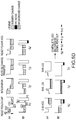
- FIG. 1 is a diagram of an illustrative electronic device having an image sensor in accordance with an embodiment.
- FIG. 2 is a diagram of an illustrative pixel array and associated row and column control circuitry for reading out image signals from an image sensor in accordance with an embodiment.
- FIG. 3 is a diagram of an illustrative image pixel readout scheme that uses a first storage node to acquire scenery information and a second storage node to accumulate charge generated from parasitic light and dark noise in parallel with the first storage node in accordance with an embodiment.
- FIG. 4 is a diagram of an illustrative image pixel readout scheme that uses a single storage node to accumulate charge generated from parasitic light and dark noise in a first period and then to capture scenery information in a second period following the first period in accordance with an embodiment.
- FIG. 5A is a circuit diagram of an illustrative image sensor pixel having at least two storage diodes and two overflow capacitors to implement the pixel readout scheme shown in FIG. 3 in accordance with an embodiment.
- FIG. 5B is a top layout view of the illustrative image sensor pixel shown in FIG. 5A in accordance with an embodiment.
- FIG. 5C is a timing diagram showing the behavior of signals for operating the image sensor pixel shown in FIG. 5A in accordance with an embodiment.
- FIG. 5D is a potential diagram illustrating the flow of charge at different time slices of the operation shown in FIG. 5C in accordance with an embodiments.
- FIG. 6 is a circuit diagram of an illustrative image sensor pixel having at least two storage diodes, two overflow capacitors, and two dual conversion gates in accordance with an embodiment.
- FIG. 7 is a circuit diagram of an illustrative image sensor pixel having at least two storage gate based charge storage nodes, two overflow capacitors, and two dual conversion gates in accordance with an embodiment.
- FIG. 8A is a circuit diagram of an illustrative image sensor pixel having at least two storage gates and a single overflow capacitor in accordance with an embodiment.
- FIG. 8B is a top layout view of the illustrative image sensor pixel shown in FIG. 8A in accordance with an embodiment.
- FIG. 8C is a timing diagram showing the behavior of signals for operating the image sensor pixel shown in FIG. 8A in accordance with an embodiment.
- FIG. 8D is a potential diagram illustrating the flow of charge at different time slices of the operation shown in FIG. 8C in accordance with an embodiments.
- FIGS. 9A and 9B are cross-sectional side views of a backside illuminated (BSI) image sensor pixel having backside light diffracting structures in accordance with an embodiment.
- BSI backside illuminated
- FIGS. 10A, 10B and 10C are top layout views showing how one or more microlenses may be formed over an image sensor pixel with two charge storage nodes in accordance with an embodiment.
- FIG. 11 is a cross-sectional side view of an illustrative image sensor pixel with two charge storage nodes, backside optical diffracting structures, and multiple microlenses formed over the backside surface to help distribute parasitic light evenly to the two charge storage nodes in accordance with an embodiment.
- Embodiments of the present invention relate to image sensors. It will be recognized by one skilled in the art that the present exemplary embodiments may be practiced without some or all of these specific details. In other instances, well-known operations have not been described in detail in order not to unnecessarily obscure the present embodiments.
- Electronic devices such as digital cameras, computers, cellular telephones, and other electronic devices may include image sensors that gather incoming light to capture an image.
- the image sensors may include arrays of pixels.
- the pixels in the image sensors may include photosensitive elements such as photodiodes that convert the incoming light into image signals.
- Image sensors may have any number of pixels (e.g., hundreds or thousands or more).
- a typical image sensor may, for example, have hundreds or thousands or millions of pixels (e.g., megapixels).
- Image sensors may include control circuitry such as circuitry for operating the pixels and readout circuitry for reading out image signals corresponding to the electric charge generated by the photosensitive elements.
- FIG. 1 is a diagram of an illustrative imaging and response system including an imaging system that uses an image sensor to capture images.
- System 100 of FIG. 1 may be an electronic device such as a camera, a cellular telephone, a video camera, or other electronic device that captures digital image data, may be a vehicle safety system (e.g., an active braking system or other vehicle safety system), or may be a surveillance system.
- vehicle safety system e.g., an active braking system or other vehicle safety system
- surveillance system e.g., a surveillance system.
- system 100 may include an imaging system such as imaging system 10 and host subsystems such as host subsystem 20 .
- Imaging system 10 may include camera module 12 .
- Camera module 12 may include one or more image sensors 14 and one or more lenses.
- Each image sensor in camera module 12 may be identical or there may be different types of image sensors in a given image sensor array integrated circuit.
- each lens may focus light onto an associated image sensor 14 .
- Image sensor 14 may include photosensitive elements (i.e., image sensor pixels) that convert the light into digital data.
- Image sensors may have any number of pixels (e.g., hundreds, thousands, millions, or more).
- a typical image sensor may, for example, have millions of pixels (e.g., megapixels).
- image sensor 14 may further include bias circuitry (e.g., source follower load circuits), sample and hold circuitry, correlated double sampling (CDS) circuitry, amplifier circuitry, analog-to-digital converter circuitry, data output circuitry, memory (e.g., buffer circuitry), address circuitry, etc.
- bias circuitry e.g., source follower load circuits
- sample and hold circuitry sample and hold circuitry
- CDS correlated double sampling circuitry
- amplifier circuitry e.g., analog-to-digital converter circuitry
- data output circuitry e.g., data output circuitry
- memory e.g., buffer circuitry
- Still and video image data from camera sensor 14 may be provided to image processing and data formatting circuitry 16 via path 28 .
- Image processing and data formatting circuitry 16 may be used to perform image processing functions such as data formatting, adjusting white balance and exposure, implementing video image stabilization, face detection, etc.
- Image processing and data formatting circuitry 16 may also be used to compress raw camera image files if desired (e.g., to Joint Photographic Experts Group or JPEG format).
- a typical arrangement which is sometimes referred to as a system on chip (SoC) arrangement
- camera sensor 14 and image processing and data formatting circuitry 16 are implemented on a common semiconductor substrate (e.g., a common silicon image sensor integrated circuit die).
- SoC system on chip
- camera sensor 14 and image processing and data formatting circuitry 16 may be formed on separate semiconductor substrates.
- camera sensor 14 and image processing circuitry 16 may be formed on separate substrates that have been stacked.
- Imaging system 10 may convey acquired image data to host subsystem 20 over path 18 .
- Host subsystem 20 may include processing software for detecting objects in images, detecting motion of objects between image frames, determining distances to objects in images, filtering or otherwise processing images provided by imaging system 10 .
- system 100 may provide a user with numerous high-level functions.
- host subsystem 20 of system 100 may have input-output devices 22 such as keypads, input-output ports, joysticks, and displays and storage and processing circuitry 24 .
- Storage and processing circuitry 24 may include volatile and nonvolatile memory (e.g., random-access memory, flash memory, hard drives, solid-state drives, etc.).
- Storage and processing circuitry 24 may also include microprocessors, microcontrollers, digital signal processors, application specific integrated circuits, etc.
- image sensor 14 may include control and processing circuitry 44 .
- Control and processing circuitry 44 (sometimes referred to as control and processing logic) may sometimes be considered part of image processing and data formatting circuitry 16 in FIG. 1 .
- Image sensor 14 may include a pixel array such as array 32 of pixels 34 (sometimes referred to herein as image sensor pixels, imaging pixels, or image pixels).
- Control and processing circuitry 44 may be coupled to row control circuitry 40 via control path 27 and may be coupled to column control and readout circuits 42 via data path 26 .
- Row control circuitry 40 may receive row addresses from control and processing circuitry 44 and may supply corresponding row control signals to image pixels 34 over control paths 36 (e.g., pixel reset control signals, charge transfer control signals, blooming control signals, row select control signals, dual conversion gain control signals, or any other desired pixel control signals).
- control paths 36 e.g., pixel reset control signals, charge transfer control signals, blooming control signals, row select control signals, dual conversion gain control signals, or any other desired pixel control signals.
- Column control and readout circuitry 42 may be coupled to the columns of pixel array 32 via one or more conductive lines such as column lines 38 .
- Column lines 38 may be coupled to each column of image pixels 34 in image pixel array 32 (e.g., each column of pixels may be coupled to a corresponding column line 38 ).
- Column lines 38 may be used for reading out image signals from image pixels 34 and for supplying bias signals (e.g., bias currents or bias voltages) to image pixels 34 .
- bias signals e.g., bias currents or bias voltages
- Column readout circuitry 42 may include column circuitry such as column amplifiers for amplifying signals read out from array 32 , sample and hold circuitry for sampling and storing signals read out from array 32 , analog-to-digital converter circuits for converting read out analog signals to corresponding digital signals, and column memory for storing the read out signals and any other desired data.
- Column control and readout circuitry 42 may output digital pixel readout values to control and processing logic 44 over line 26 .
- Array 32 may have any number of rows and columns. In general, the size of array 32 and the number of rows and columns in array 32 will depend on the particular implementation of image sensor 14 . While rows and columns are generally described herein as being horizontal and vertical, respectively, rows and columns may refer to any grid-like structure (e.g., features described herein as rows may be arranged vertically and features described herein as columns may be arranged horizontally).
- BSI backside illuminated
- FSI front side illuminated
- BSI pixels that uses the global shutter (GS) readout method that relies on charge domain storage nodes often suffer from low global shutter efficiency due to difficulties in shielding in-pixel charge storage nodes from parasitic light.
- “Parasitic light” is defined as photons entering an image pixel during times other than the intended integration period, which then generate charge that is inadvertently collected by the pixel storage.
- parasitic light charge This additional charge generated by the parasitic light (sometimes referred to as “parasitic light charge”) will be added to the scenery image charge (i.e., charge collected from the scene during the proper integration time), which will create ghosting, smearing, or other undesired colorized effects if something in the scenery to be captured is moving.
- the parasitic light charge may create undesired vertical shading as rows are read out sequentially from the top of the array to the bottom of the array.
- conventional image sensor pixels are not able to mitigate the effects of parasitic light while offering high dynamic range, which is a desirable feature in many imaging applications.
- an image sensor pixel architecture is provided that is capable of providing both an improvement to global shutter efficiency (GSE) and high dynamic range (HDR) operation without generating any motion artifacts.
- FIG. 3 is a diagram of an illustrative image pixel readout architecture that uses a first storage node to acquire scenery information and a second storage node to accumulate charge generated from parasitic light and dark noise in parallel with the first storage node.
- image sensor pixel 34 may include a photosensitive element such as photodiode 300 , a first storage node such as storage node 302 configured to capture scenery information, and a second storage node such as storage node 304 configured to accumulate charge generated from background signals such as parasitic light and dark noise signals.
- Photodiode 300 may be configured to accumulate charge generated by photons emanating from the scenery to be captured during an integration time.
- the scenery-generated charge may be conveyed from photodiode 300 to first storage node 302 .
- Storage node 302 may include a charge storage region 310 that receives the scenery-generated charge from photodiode 300 and stores a corresponding amount of charge E 1 . Any amount of charge exceeding a first predetermined threshold amount may spill over to overflow storage region 312 , which will end up storing a corresponding amount of overflow charge E 2 .
- Charge E 1 therefore corresponds to a low light signal, whereas charge E 2 corresponds to a high light signal.
- Overflow charge storage region 312 therefore provides first storage node 302 with HDR capabilities with a single PD exposure.
- First storage node 302 operated in this way is therefore sometimes referred to as a scenery HDR storage node.
- Storage node 304 may accumulate parasitic light charge and dark noise signals in parallel. The amount of dark noise is generally dependent on the operating temperature and is typically not related to the amount of light being generated within pixel 34 .
- Storage node 304 may include a charge storage region 320 and an overflow charge storage region 322 that receive the parasitic light charge and the dark noise charge (sometimes referred to collectively as background charge or background signals).
- Storage region 320 stores a corresponding amount of charge E 1 ′.
- Second storage node 304 operated in this way is therefore sometimes referred to as a background HDR storage node.
- charge E 1 ′ read out from charge storage region 320 may be subtracted from charge E 1 read out from charge storage region 310 using a subtraction circuit 330 to generate a first corrected non-overflow signal E 1 corr.
- charge E 2 ′ read out from charge storage region 322 may be subtracted from charge E 2 read out from charge storage region 312 using a subtraction circuit 332 to generate a second corrected overflow signal E 2 corr.
- Corrected signals E 1 corr and E 2 corr may then be combined via a linearization process to output the final HDR output signal.
- Subtraction circuits 330 and 332 and the linearizing component may be formed as part of control and processing logic 44 ( FIG.
- FIG. 4 is a diagram of another illustrative image pixel readout architecture that uses a single storage node 402 to accumulate charge generated from parasitic light and dark noise in a first period and then to capture scenery information in a second period following the first period (i.e., the two signal captures are acquired sequentially instead of in parallel).
- image sensor pixel 34 may include a photosensitive element such as photodiode 400 and a single dual-purpose storage node such as storage node 402 .
- storage node 402 may accumulate parasitic light charge and dark noise signals.
- Storage node 402 may include a charge storage region 410 that receives the background signals (e.g., the parasitic light charge and the dark noise charge) and stores a corresponding amount of charge E 1 ′. Any amount of charge exceeding a given predetermined threshold amount may spill over to overflow storage region 412 , which also receives the background signals (e.g., the parasitic light charge and the dark noise charge) and will end up storing a corresponding amount of overflow and background charge E 2 ′.
- Overflow charge storage region 412 provides storage node 402 with HDR capabilities. Storage node 402 operated in this way is therefore sometimes referred to as an HDR storage node.
- storage node 402 may receive scenery-generated charge from photodiode 400 accumulated during an integration time.
- charge storage region 410 may receive the scenery-generated charge from photodiode 400 and store a corresponding amount of charge E 1 . Any amount of charge exceeding the given predetermined threshold amount may spill over to overflow storage region 412 , which will end up storing a corresponding amount of overflow charge E 2 .
- Charge E 1 ′ generated during the first phase may be read out and then signal delayed by a first delay buffer 420
- charge E 2 ′ generated during the second phase may be read out and then signal delayed by a second delay buffer 422 . Delayed in this way, signal E 1 ′ obtained during the first phase may be subtracted from signal E 1 obtained during the second phase using a subtraction circuit 430 to generate a first corrected non-overflow signal E 1 corr.
- signal E 2 ′ obtained during the first phase may be subtracted from signal E 2 obtained during the second phase using a subtraction circuit 432 to generate a second corrected overflow signal E 2 corr. Corrected signals E 1 corr and E 2 corr may then be combined via a linearization process to output the final HDR output signal.
- Delay circuits 420 and 422 , subtraction circuits 430 and 432 , and the linearization component may be formed as part of control and processing logic 44 ( FIG. 2 ) on image sensor die 14 or as part of image processing and data formatting circuitry 16 ( FIG. 1 ) separate from image sensor 14 . Subtracting the accumulated background signals from the scenery signals in this sequential manner enables GSE improvement, reduced dark signal non-uniformity, and HDR operation while minimizing any undesired motion artifacts.
- FIG. 5A shows one suitable circuit implementation supporting the pixel readout architecture of the type described in connection with FIG. 3 .
- image pixel 34 may represent a global shutter pixel with a pinned photodiode PD coupled to an anti-blooming transistor that is partially activated using control signal AB in order to draw away blooming charge from the photodiode.
- the anti-blooming transistor may also be fully activated using control signal AB to reset the photodiode.
- Photodiode PD may be coupled to a first storage diode SD 1 via a first output gate transistor controlled by signal OG 1 .
- Storage diode SD 1 may be coupled to a first overflow capacitor CAP 1 via a first overflow gate (or coupling gate) transistor controlled by signal CG 1 .
- Storage diode SD 1 may also be coupled to a floating diffusion node FD via a first transfer gate transistor controlled by signal TX 1 .
- Photodiode PD may also be coupled to a second storage diode SD 2 via a second output gate transistor controlled by signal OG 2 .
- Storage diode SD 2 may be coupled to a second overflow capacitor CAP 2 via a second overflow gate (or coupling gate) transistor controlled by signal CG 2 .
- Storage diode SD 2 may also be coupled to floating diffusion node FD via a second transfer gate transistor controlled by signal TX 2 .
- Overflow capacitors CAP 1 and CAP 2 may be implemented using high density metal-insulator-metal (MIM) capacitive structures configured to support more than 100 dB of dynamic range (as an example). In general, any suitable integrated circuit capacitor structure may be used within pixel 34 .
- MIM metal-insulator-metal
- floating diffusion node FD Any charge transferred to floating diffusion node FD causes the potential on this node to change, and this change is sensed by the source follower transistor SF.
- the source terminal of the source follower transistor is connected via a row select transistor to the sensor array column sensing line 38 that delivers the pixel signal to the periphery of the array for further processing.
- Control signal RS is asserted to activate the row select transistor to transfer the pixel signal to column sensing line 38 .
- floating diffusion node FD may be reset to supply voltage Vaa (e.g., a nominal positive power supply voltage provided on power supply line 580 ) by asserting control signal RST to turn on the reset transistor.
- supply voltage Vaa e.g., a nominal positive power supply voltage provided on power supply line 580
- storage diodes SD 1 and SD 2 can be reset at the same time as the floating diffusion node by simultaneously asserting signals RST, TX 1 , and/or TX 2 .
- storage diode SD 1 may be configured to store low scenery light charge E 1 (see FIG. 3 ) and capacitor CAP 1 may be configured to store high scenery light charge E 2
- storage diode SD 2 may be configured to store background light charge E 1 ′
- capacitor CAP 2 may be configured to store backlight light charge E 2 ′.
- storage diode SD 1 implements charge storage region 310 while CAP 1 implements overflow charge storage region 312
- storage diode SD 2 implements charge storage region 320 while CAP 2 implements overflow charge storage region 322 .
- the global shutter image sensor pixel 34 shown in FIG. 5A is merely illustrative and is not intended to limit the scope of the present embodiments. This pixel scheme may be extended or applied to pixel architectures with three, four, or more charge storage nodes/regions per pixel. In general, global shutter image sensor pixel 34 may include any number of charge storage regions and any number of associated charge transfer, charge resetting, readout, and selection transistors for supporting a global shutter readout operation.
- FIG. 5B is a top layout view of the illustrative image sensor pixel shown in FIG. 5A .
- pixel 34 may be substantially symmetrical about symmetry line 550 (except for the reset, source follower, and row select transistors), where the anti-blooming transistor and the floating diffusion node may be bisected by the symmetry line 550 .
- the first output gate, the first transfer gate, the first storage diode, the first overflow gate, and the reset transistor may be formed on one side of the symmetry line 550
- the second output gate, the second transfer gate, the second storage diode, the second overflow gate, the source follower transistor, and the reset transistor may be formed on the other side of the symmetry line 550 .
- FIG. 5C is a timing diagram showing the behavior of signals for operating the image sensor pixel shown in FIG. 5A .
- anti-blooming gate control signal AB, reset signal RST, transfer gate control signals TX 1 and TX 2 , and overflow gate control signals CG 1 and CG 2 may be pulsed high to reset photodiode PD, the two storage diodes SD 1 and SD 2 , and the overflow capacitors CAP 1 and CAP 2 .
- the period following time t 1 i.e., the time period between t 1 and t 4
- control signals OG 1 , CG 1 , and CG 2 may be raised to an intermediate voltage level (e.g., some static voltage level between positive power supply voltage Vaa and ground Vss) or may be repeatedly/partially pulsed. Pulsing or partially activating OG 1 during integration allows the photon-generated charge to overflow from the photodiode into storage diode SD 1 when the photodiode is full. Pulsing or partially activating CG 1 and CG 2 would allow excess charge in storage diodes SD 1 and SD 2 to overflow to corresponding capacitors CAP 1 and CAP 2 when the storage diodes become full.
- an intermediate voltage level e.g., some static voltage level between positive power supply voltage Vaa and ground Vss
- signal OG 1 may be fully asserted to perform a global transfer of charge from all of the photodiodes into their corresponding storage diodes SD 1 .
- reset signal RST may be pulsed high to reset the floating diffusion node.
- row select signal RS may be pulsed high to obtain a sample-and-hold reset (SHR) signal for the reset floating diffusion node.
- transfer signal TX 1 may be driven high to transfer the low light signal from storage diode SD 1 to the floating diffusion node.
- row select signal RS may be pulsed high to obtain a sample-and-hold sensor (SHS) signal for the charge previously stored in storage diode SD 1 .
- SHS sample-and-hold sensor
- the signal values obtained at times t 4 ′ and t 5 ′ may be subtracted using a correlated double sampling (CDS) method to compute the final output signal for storage diode SD 1 . Since the charge stored in storage diode SD 1 represents low light, high conversion gain is sometimes needed to amplify the low light signals. Thus, signal readout mechanisms associated with SD 1 is sometimes referred to as high conversion gain (HCG) SHR and SHS operations.
- HCG high conversion gain
- control signal CG 1 may be pulsed high to transfer all the overflow charge (e.g., the high light signals) from capacitor CAP 1 to storage diode SD 1 and to floating diffusion FD.
- row select signal RS may be pulsed high to obtain a sample-and-hold sensor (SHS) signal for charge that represents the sum of charge previously stored in storage diode SD 1 and capacitor CAP 1 .
- reset signal RST may be pulsed high to reset the floating diffusion node.
- row select signal RS may be pulsed high to obtain a sample-and-hold reset (SHR) signal for the reset floating diffusion node.
- SHR sample-and-hold reset
- the signal values obtained at times t 6 ′ and t 7 ′ may be subtracted using a double sampling (DS) method to compute the final output signal corresponding to the sum of charge from SD 1 and CAP 1 (i.e., the sum of both low light and high light signals). Since the charge stored in CAP 1 represents high light, low conversion gain is used to process the high light signals. Thus, signal readout mechanisms associated with (SD 1 +CAP 1 ) is sometimes referred to as low conversion gain (LCG) SHR and SHS operations.
- DS double sampling
- This process may be repeated when reading out the background signals accumulated using second storage diode SD 2 .
- reset signal RST may be pulsed high to again reset the floating diffusion node.
- row select signal RS may be pulsed high to obtain an SHR signal for the reset floating diffusion node.
- transfer signal TX 2 may be driven high to transfer background charge (e.g., charge generated as a result of parasitic light and dark noise current) from storage diode SD 2 to the floating diffusion node.
- row select signal RS may be pulsed high to obtain an SHS signal for the charge previously stored in storage diode SD 2 .
- the signal values obtained at times t 8 ′ and t 9 ′ may be subtracted using a correlated double sampling (CDS) method to compute the final output signal for storage diode SD 2 .
- CDS correlated double sampling
- control signal CG 2 may be pulsed high to transfer all the overflow charge from capacitor CAP 2 to storage diode SD 2 and to floating diffusion FD.
- row select signal RS may be pulsed high to obtain an SHS signal for charge that represents the sum of charge previously stored in storage diode SD 2 and capacitor CAP 2 .
- reset signal RST may be pulsed high to reset the floating diffusion node.
- row select signal RS may be pulsed high to obtain an SHR signal for the reset floating diffusion node.
- the signal values obtained at times t 10 ′ and t 11 ′ may be subtracted using a double sampling (DS) method to compute the final output signal corresponding to the sum of charge from SD 2 and CAP 2 .
- DS double sampling
- FIG. 5D is a potential diagram illustrating the flow of charge at different time slices of the operation shown in FIG. 5C .
- FIG. 5D shows both the potential profile along the cross-section of pixel 34 cut along line AA′ (see FIG. 5B ) and along the cross-section of pixel 34 cut along line BB′.
- time t 1 all storage regions are reset so that any existing signal charge is drained.
- photodiode PD may fill up.
- storage diode SD 1 may fill up as well. Since CG 1 is pulsed or partially raised, capacitor CAP 1 may also accumulate charge.
- OG 1 is pulsed high to transfer all charge from photodiode PD to storage diode SD 1 .
- the floating diffusion node may be reset.
- thermal noise sometimes referred to as sampling noise or KTC noise
- background charge may also accumulate in SD 1 and CAP 1 .
- SHR of the HCG signal associated with only SD 1 may be read out.
- TX 1 may be asserted to transfer all charge from SD 1 to FD while high light charge is retained in CAP 1 . Thereafter SHS of the HCG signal associated with only SD 1 may be read out. These SHR and SHS may be subtracted using a correlated double sampling (CDS) method to compute the final output signal for storage diode SD 1 .
- CDS correlated double sampling
- CG 1 may be asserted to transfer all charge from CAP 1 to SD 1 and then to FD since TX 1 is still asserted. As a result, the sum of charge from SD 1 and CAP 1 are now present in FD. At this point, SHS of the LCG signal associated with (SD 1 +CAP 1 ) may be read out.
- RST may be asserted to drain out all signal charge from the pixel while leaving only KTC noise.
- SHR of the LCG signal associated with (SD 1 +CAP 1 ) may be read out. Double sampling may be separately performed for the SHS and SHR signals to compute the final output signal corresponding to the sum of charge from SD 1 and CAP 1 . Processing may continue (see, e.g., time t 8411 in FIG. 5C ) to perform readout for only the background signal charge.
- Computing the difference in signal values obtained during time t 1 ⁇ t 7 versus signal values obtained during time t 8411 can therefore remove any unwanted contribution from the background charge (e.g., to reduce any potential signal inaccuracies due to parasitic light and/or dark signal non-uniformity).
- FIG. 6 is a circuit diagram showing another suitable implementation of pixel 34 .
- the pixel architecture of FIG. 6 further includes a first dual conversion gate (e.g., the transistor controlled by signal DCG 1 ) that couples capacitor CAP 1 directly to the floating diffusion node and a second dual conversion gate (e.g., the transistor controlled by signal DCG 2 ) that couples capacitor CAP 2 directly to the floating diffusion node.
- the addition of the dual conversion gates provides pixel 34 with the ability to selectively reset the overflow capacitors CAP 1 and/or CAP 2 during integration to a higher potential, thereby further extending the dynamic range of pixel 34 .
- FIG. 7 is a circuit diagram showing another suitable implementation of pixel 34 .
- the pixel architecture of FIG. 7 uses storage gates in lieu of the output gate and storage diode pair.
- a first storage gate that is controlled by signal SG 1 replaces the first output gate and the first storage diode SD 1
- a second storage gate that is controlled by signal SG 2 replaces the second output gate and the second storage diode SD 2 .
- the inclusion of the dual conversion gates provides pixel 34 with the ability to selectively reset the overflow capacitors CAP 1 and/or CAP 2 during the exposure period to a higher potential, thereby further extending the dynamic range of pixel 34 .
- FIG. 8A is a circuit diagram illustrating yet another suitable arrangement of pixel 34 .
- image pixel 34 may represent a global shutter pixel with pinned photodiode PD that is coupled to a single shared overflow capacitor CAP* (e.g., a MIM capacitor) via an anti-blooming transistor controlled by control signal AB.
- Photodiode PD may be coupled to a first storage gate controlled by signal SG 1 and also to a second storage gate controlled by signal SG 2 . Similar to the embodiment of FIG. 7 , the first storage gate performs the function of the first output gate and the first storage diode SD 1 (see FIG.
- the first storage gate may be coupled to the floating diffusion node FD via a first transfer gate (e.g., a first charge transfer transistor controlled by transfer signal TX 1 ), whereas the second storage gate may be coupled to the floating diffusion node FD via a second transfer gate (e.g., a second charge transfer transistor controlled by transfer signal TX 2 ).
- a first transfer gate e.g., a first charge transfer transistor controlled by transfer signal TX 1
- TX 2 e.g., a second charge transfer transistor controlled by transfer signal
- Any charge transferred to floating diffusion node FD causes the potential on this node to change, and this potential change is sensed by the source follower transistor SF.
- the source terminal of the source follower transistor is connected via a row select transistor to the sensor array column sensing line 38 that delivers the pixel signal to the periphery of the array for further processing.
- Control signal RS is asserted to activate the row select transistor to transfer the pixel signal to column sensing line 38 .
- a dual conversion gate (e.g., the transistor controlled by signal DCG) may be coupled between floating diffusion node FD and the reset transistor.
- floating diffusion node FD may be reset to supply voltage Vaa (e.g., a nominal positive power supply voltage provided on power supply line 580 ) by asserting control signal RST to turn on the reset transistor and asserting control signal DCG to turn on the DCG transistor.
- Vaa e.g., a nominal positive power supply voltage provided on power supply line 580
- overflow capacitor CAP* may be coupled to the node interposed between the dual conversion gate and the reset transistor (i.e., node 810 ) via a low gain transistor controlled by signal LG.
- Overflow capacitor CAP* which stores high light signals, is only coupled to node 810 during a low gain phase by selectively asserting signal LG.
- the second storage gate may be configured to store low scenery light charge E 1 (see FIG. 3 ), whereas the first storage gate may be configured to store low background light charge E 1 ′.
- Pixel 34 can still support HDR functionality but cannot support cancellation of the background parasitic/dark noise charge associated with the high light signals.
- the global shutter image sensor pixel 34 shown in FIG. 8A is merely illustrative and is not intended to limit the scope of the present embodiments. This pixel scheme may be extended or applied to pixel architectures with three, four, or more charge storage nodes/regions per pixel implemented using storage diodes or other suitable types of charge storage means. In general, global shutter image sensor pixel 34 may include any number of charge storage regions, any number of shared or unshared overflow capacitors, and any number of associated charge transfer, charge resetting, readout, and selection transistors for supporting a global shutter readout operation.
- FIG. 8B is a top layout view of the illustrative image sensor pixel shown in FIG. 8A .
- pixel 34 may be substantially symmetrical about symmetry line 850 (if ignoring the DCG, LG, RST, SF, and RS transistors), where the anti-blooming transistor and the floating diffusion node are bisected by the symmetry line 850 .
- the first transfer gate, the first storage gate, the low gain transistor, and the dual conversion gate may be formed on one side of the symmetry line 550
- the second transfer gate, the second storage gate, the row select transistor, the source follower transistor, and the reset transistor may be formed on the other side of the symmetry line 850 .
- FIG. 8C is a timing diagram showing the behavior of signals for operating the image sensor pixel shown in FIG. 8A .
- anti-blooming gate control signal AB, reset signal RST, and the low gain control signal LG may be pulsed high to reset photodiode PD and also the overflow capacitor CAP*.
- the period following time t 1 i.e., the time period between t 1 and t 4
- anti-blooming control signal AB may be repeatedly partially pulsed or raised to an intermediate voltage level (e.g., some static voltage level between positive power supply voltage Vaa and ground Vss). Pulsing or partially activating AB during integration allows the photon-generated charge to overflow from the photodiode into the overflow capacitor CAP* when the photodiode is full, such as up to time t 5 .
- an intermediate voltage level e.g., some static voltage level between positive power supply voltage Vaa and ground Vss.
- control signals RST, DCG, TX 1 and TX 2 may all be pulsed high to reset the floating diffusion node, the first storage gate, and the second storage node. Note that the storage gates are drained through the floating diffusion node via the two intervening charge transfer gates.
- signals RST, TX 1 , and TX 2 are low, but signal DCG may continue to be asserted until a subsequent global charge transfer has completed at time t 5 .
- low gain control signal LG and second storage gate control signal SG 2 may be pulsed high to perform a global charge transfer from the photodiode PD to the second storage gate and from the overflow capacitor CAP* to node 810 . Since DCG is also high at this time, the overflow signal from CAP* is also transferred to the floating diffusion node via the dual conversion gate.
- row select signal RS may be pulsed high to obtain a sample-and-hold sensor (SHS) signal equivalent to the charge previously stored in capacitor CAP*.
- control signals RST and DCG may be pulsed high to reset the floating diffusion node.
- row select signal RS may be pulsed high to obtain a sample-and-hold reset (SHR) signal for the reset floating diffusion node.
- SHR sample-and-hold reset
- the signal values obtained at times t 5 ′ and t 6 ′ may be subtracted using the double sampling (DS) method to compute the final output signal for the overflow (high light) charge.
- transfer signal TX 2 may be pulsed high to transfer scenery charge accumulated at the second storage gate to the floating diffusion node.
- row select signal RS may again be pulsed high to obtain an SHS signal for the charge previously stored in the second storage gate.
- the signal values obtained at times t 6 ′ and t 7 ′ may be subtracted using the correlated double sampling (CDS) method to compute the final output (low light scenery) signal associated with the second storage gate.
- CDS correlated double sampling
- control signals RST and DCG may be pulsed high to reset the floating diffusion node.
- row select signal RS may be pulsed high to obtain a sample-and-hold reset (SHR) signal for the reset floating diffusion node.
- SHR sample-and-hold reset
- transfer signal TX 1 may be pulsed high to transfer background charge accumulated at the first storage gate to the floating diffusion node.
- row select signal RS may again be pulsed high to obtain an SHS signal for the charge previously stored in the first storage gate.
- the signal values obtained at times t 8 ′′ and t 9 ′ may be subtracted using the correlated double sampling (CDS) method to compute the final output (parasitic light and dark noise) signal associated with the first storage gate.
- CDS correlated double sampling
- FIG. 8D is a potential diagram illustrating the flow of charge at different time slices of the operation shown in FIG. 8C .
- the storage regions e.g., the overflow capacitor region, the photodiode region, etc.
- photodiode PD may fill up.
- overflow capacitor CAP* may start filling up as well.
- background charge e.g., charge generated as a result of parasitic light and/or dark current
- the storage gate regions are drained through the floating diffusion node via the two intervening charge transfer gates.
- the transfer gate potentials (TX 1 /TX 2 ) are raised back high. The thermal KTC noise may remain in the floating diffusion node.
- low gain control signal LG and second storage gate control signal SG 2 may be pulsed high to perform a global charge transfer from the photodiode PD to the second storage gate and from the overflow capacitor CAP* to node 810 . Since DCG is also high at this time, the overflow signal from CAP* is also transferred to the floating diffusion node via the dual conversion gate. Note that the potential of the first storage gate is not affected at this time.
- the floating diffusion node is reset while the scenery charge remains trapped in the second storage gate region.
- the scenery charge may be transferred from the second storage gate region to the floating diffusion node and then read out using CDS.
- the first storage gate still holds the background charge.
- the background charge may be transferred from the first storage gate region to the floating diffusion node and then read out using CDS.
- the two correlated double sampled signals may then be subtracted from one another (e.g., the second CDS signal may be subtracted from the first CDS signal) to cancel out the background signal contribution for the low light signals.
- FIG. 9A is a cross-sectional side view of an illustrative BSI pixel 34 .
- pixel 34 may be formed using a semiconductor substrate 900 and may include a photodiode PD formed from the front side (or front surface) 902 of substrate 900 , storage nodes 910 (e.g., storage regions associated with the storage diodes of FIGS. 5-6 or the storage gates of FIGS.
- STI shallow trench isolation
- backside deep trench isolation (BDTI) structures may be formed to provide electrical and optical isolation between adjacent pixels and also to protect the charge storage regions and the floating diffusion region from incoming light.
- An optical shielding structure such as metal shield 920 may be formed on the back side 904 of the substrate to provide additional shielding.
- metal shield 920 may at least partially cover or completely cover the charge storage regions and/or the floating diffusion region of pixel 34 .
- metal shielding structure 920 may form a metal grid over the back surface of substrate 900 with slots or openings aligned to the footprint of the photodiode regions to allow incoming light to reach the photodiodes.
- incoming light enters pixels 34 from the back surface 904 of the substrate (as indicated by arrow 950 ) and is preferably absorbed within photodiode region PD.
- the incoming light 950 is fully absorbed within photodiode PD and never reaches the two storage regions.
- the incoming light 950 can sometimes inadvertently leak into one or more of the storage regions 910 . This light leakage is especially problematic for pixel arrangements that depend on the design of two different storage nodes such as the pixel architectures of FIGS. 3-8 .
- optical diffracting structures such as light diffracting structures 930 may be formed at the back side of substrate 900 (see, e.g., FIG. 9A ).
- Light diffracting structures 930 may be implemented as an array of pyramidal structures, conical structures, funnel-shaped structures, triangular-shaped structures, or may have other suitable shapes and may be formed using silicon, silicon dioxide, silica-based ceramic materials, inorganic/organic polymers, or other suitable dielectric material.
- optical diffracting structures 930 can help ensure that the same amount of stray or parasitic light is distributed evenly between the two intra-pixel storage regions (e.g., by further randomizing the trajectory of light within the pixel), which improves the noise cancellation performance of pixel 34 .
- the metal shield 920 can be made with larger openings as illustrated in the example of FIG. 9B .
- metal shield 920 no longer cover the storage and floating diffusion regions and since the metal shield slots are wider, the photodiode region can extend at least partially under the storage regions, which helps further improve global shutter efficiency.
- the optical diffracting structures 932 may also be extended under the entire footprint of the pixel to ensure that light is evenly distributed between the two charge storage regions.
- FIGS. 10A, 10B and 10C are top layout views showing how one or more microlenses may be formed over an image sensor pixel with two or more charge storage nodes.
- a single microlens 1000 may be formed over pixel 34 .
- the center of microlens 1000 may be aligned to corresponding photodiode of pixel 34 .
- FIG. 10 in which pixel 34 includes two storage diodes SG 1 and SG 2 such as the embodiments of FIGS. 7 and 8 is merely illustrative.
- pixel 34 may include multiple charge storage nodes implemented as storage diodes or other types of charge storage regions.
- FIG. 10B illustrates another suitable arrangement in which image pixel 34 is provided with four separate microlenses 1002 (e.g., four circular microlenses of the same size).
- the inclusion of multiple microlenses may provide better optical symmetry between the four quadrants of pixel 34 , which can help ensure that parasitic light charge is equally distributed between the two storage gate regions.
- at least two of the microlenses 1002 may at least partially cover or overlap with storage gate regions SG 1 and SG 2 . This is, however, merely illustrative. In other suitable embodiments, storage gates SG 1 and SG 2 may not be covered by any microlenses (e.g., microlenses 1002 are non-overlapping with the storage gate regions).
- FIG. 10C illustrates yet another suitable arrangement in which image pixel 34 is provided with only two separate microlenses 1004 (e.g., two oval microlenses of the same size).
- a first of the two microlenses 1004 may be aligned with the first storage gate region, whereas a second of the two microlenses 1004 may be aligned with the second storage gate region.
- the inclusion of multiple microlenses may provide better optical symmetry between the two halves of pixel 34 , which can help ensure that parasitic light charge is equally distributed between the two storage gate regions.
- both microlenses 1004 may at least partially cover or overlap with storage gate regions SG 1 and SG 2 . This is, however, merely illustrative. In other suitable embodiments, storage gates SG 1 and SG 2 need not be covered by any microlenses (e.g., microlenses 1004 are non-overlapping with the storage gate regions).
- the number of microlenses may be adjusted depending on the number of charge storage regions in pixel 34 .
- a BSI image pixel with two charge storage regions may include two or more microlenses formed over the back surface of the substrate;
- a BSI image pixel with three charge storage regions may include three or more microlenses formed over the back surface of the substrate;
- a BSI image pixel with four charge storage regions may include four or more microlenses formed over the back surface of the substrate; etc.
- FIG. 11 is a cross-sectional side view of an illustrative image sensor pixel 34 with at least two charge storage nodes SN 1 and SN 2 , backside optical diffracting structures 934 , and multiple microlenses 1010 formed over the backside substrate surface to help distribute parasitic light evenly to the two charge storage nodes. As shown in FIG.
- a first of the two microlenses 1010 may be formed over the first storage node SN 1
- a second of the two microlenses 1010 may be formed over the second storage node SN 2 .
- Both the first and second microlenses 1010 are configured to direct incoming light towards the underlying photodiode and are also configured in a way such that any light that would be received by SN 1 and SN 2 are randomized.
- the backside light diffracting structures 934 e.g., an array of pyramidal or conical light diffracting structures formed at the back substrate surface
- the use of optical diffracting structures and/or multiple microlenses shown in FIGS. 9-11 may be applied to any of the pixel architectures described in connection with FIGS. 3-8 to help improve global shutter efficiency.
- the embodiments described herein can help improve global shutter efficiency without sacrificing HDR functionality. If desired, however, the techniques described in connection with FIGS. 3-11 can also be extended to rolling shutter image sensor pixels to improve readout operations.
- an image sensor includes a photodiode configured to accumulate charge generated by scenery light, a first storage node configured to receive and to store the accumulated charge from the photodiode, a second storage node configured to store charge generated by parasitic light and dark noise signals (sometimes referred to collectively as background signals), and circuitry configured to subtract the charge stored in the second storage node from the charge stored in the first storage node to cancel out any undesired signal contribution from the background signals.
- a photodiode configured to accumulate charge generated by scenery light
- a first storage node configured to receive and to store the accumulated charge from the photodiode
- a second storage node configured to store charge generated by parasitic light and dark noise signals (sometimes referred to collectively as background signals)
- circuitry configured to subtract the charge stored in the second storage node from the charge stored in the first storage node to cancel out any undesired signal contribution from the background signals.
- the first storage node may include a first charge storage region configured to store low scenery light signals and a first overflow storage region configured to store high scenery light signals.
- the second storage node may include a second charge storage region configured to store low parasitic light and dark noise signals and a second overflow storage region configured to store high parasitic light and dark noise signals.
- the circuitry may be configured to compute a first difference between the amount of charge stored in the first charge storage region and the amount of charge stored in the second charge storage region and also to compute a second difference between the amount of charge stored in the first overflow storage region and the amount of charge stored in the second overflow storage region. The circuitry may then combine the first computed difference with the second computed difference to obtain a high dynamic range output signal.
- the first charge storage region is a first storage diode; the first overflow storage region is a first overflow capacitor; the second charge storage region is a second storage diode; and the second overflow storage region is a second overflow capacitor.
- the image sensor may further include a first output gate coupled between the photodiode and the first storage diode, a second output gate coupled between the photodiode and the second storage diode, a first overflow gate coupled between the first storage diode and the first overflow capacitor, a second overflow gate coupled between the second storage diode and the second overflow capacitor, a first transfer gate coupled between the first storage diode and a floating diffusion region, and a second transfer gate coupled between the second storage diode and the floating diffusion region.
- the first overflow gate, the second overflow gate, and the first output gate are at least partially activated (e.g., pulsed or raised to some intermediate static voltage level) during integration time.
- the image sensor may also include a first dual conversion gate coupled between the first overflow capacitor and the floating diffusion region, and a second dual conversion gate coupled between the second overflow capacitor and the floating diffusion region.
- the storage diodes may alternatively be implemented as storage gate devices.
- the image sensor may be a backside illuminated (BSI) image sensor.
- the image sensor may further include optical diffracting structures (e.g., an array of pyramidal dielectric structures) formed at a back side of the substrate, where the optical diffracting structures are configured to randomize and distribute the parasitic light equally between the first and second storage nodes.
- optical diffracting structures e.g., an array of pyramidal dielectric structures
- one or more microlenses may be configured to direct incoming light towards the underlying photodiode and may at least partially cover or overlap with the storage node regions.
- an image sensor pixel in another embodiment, includes a photodiode configured to accumulate charge generated by scenery light and a single storage node that is configured to receive and to store charge generated by parasitic light and dark noise signals during a first phase and that is further configured to receive and to store the accumulated charge from the photodiode during a second that is different than the first phase. Additional circuitry is provided that is configured to subtract the charge obtained during the first phase from the charge obtained during the second phase to cancel out any undesired signal contribution from the parasitic light and the dark noise signals.
- the storage node may include a charge storage region configured to store low light signals and an overflow storage region configured to store high light signals to provide HDR functionality.
- an image sensor pixel in accordance with yet another suitable embodiment, includes a photodiode, a first storage gate coupled directly to the photodiode (where the first storage gate is configured to store charge generated by parasitic light and dark noise signals), a second storage gate coupled directly to the photodiode (where the second storage gate is configured to store charge generated by scenery light), a single overflow capacitor, and an anti-blooming gate coupled between the photodiode and the overflow capacitor.
- the image sensor pixel may further include a floating diffusion region, a first transfer gate coupled between the first storage gate to the floating diffusion region, and a second transfer gate coupled between the second storage gate to the floating diffusion region.
- the pixel may further include a dual conversion gate coupled between the floating diffusion region and a power supply terminal, a reset gate coupled between the dual conversion gate and the power supply terminal, and a low gain transistor coupled between the overflow capacitor and an intermediate node at which the dual conversion gate is connected to the reset gate.
- the anti-blooming gate may be at least partially activated or pulsed during integration time.
Abstract
Description
Claims (18)
Priority Applications (4)
| Application Number | Priority Date | Filing Date | Title |
|---|---|---|---|
| US16/661,009 US11218653B2 (en) | 2019-07-09 | 2019-10-23 | Methods and circuitry for improving global shutter efficiency in backside illuminated high dynamic range image sensor pixels |
| CN202010527357.0A CN112216709A (en) | 2019-07-09 | 2020-06-11 | Method and circuit for improving global shutter efficiency in backside illuminated high dynamic range image sensor pixels |
| DE102020004050.0A DE102020004050A1 (en) | 2019-07-09 | 2020-07-06 | PROCESS AND CIRCUIT ARRANGEMENTS FOR IMPROVING GLOBAL SHUTTER EFFICIENCY IN BACKLIT IMAGE SENSOR PIXELS WITH HIGH DYNAMIC SCOPE |
| US17/456,982 US11778343B2 (en) | 2019-07-09 | 2021-11-30 | Methods and circuitry for improving global shutter efficiency in backside illuminated high dynamic range image sensor pixels |
Applications Claiming Priority (2)
| Application Number | Priority Date | Filing Date | Title |
|---|---|---|---|
| US201962871899P | 2019-07-09 | 2019-07-09 | |
| US16/661,009 US11218653B2 (en) | 2019-07-09 | 2019-10-23 | Methods and circuitry for improving global shutter efficiency in backside illuminated high dynamic range image sensor pixels |
Related Child Applications (1)
| Application Number | Title | Priority Date | Filing Date |
|---|---|---|---|
| US17/456,982 Continuation US11778343B2 (en) | 2019-07-09 | 2021-11-30 | Methods and circuitry for improving global shutter efficiency in backside illuminated high dynamic range image sensor pixels |
Publications (2)
| Publication Number | Publication Date |
|---|---|
| US20210014438A1 US20210014438A1 (en) | 2021-01-14 |
| US11218653B2 true US11218653B2 (en) | 2022-01-04 |
Family
ID=74058604
Family Applications (2)
| Application Number | Title | Priority Date | Filing Date |
|---|---|---|---|
| US16/661,009 Active 2039-12-31 US11218653B2 (en) | 2019-07-09 | 2019-10-23 | Methods and circuitry for improving global shutter efficiency in backside illuminated high dynamic range image sensor pixels |
| US17/456,982 Active US11778343B2 (en) | 2019-07-09 | 2021-11-30 | Methods and circuitry for improving global shutter efficiency in backside illuminated high dynamic range image sensor pixels |
Family Applications After (1)
| Application Number | Title | Priority Date | Filing Date |
|---|---|---|---|
| US17/456,982 Active US11778343B2 (en) | 2019-07-09 | 2021-11-30 | Methods and circuitry for improving global shutter efficiency in backside illuminated high dynamic range image sensor pixels |
Country Status (3)
| Country | Link |
|---|---|
| US (2) | US11218653B2 (en) |
| CN (1) | CN112216709A (en) |
| DE (1) | DE102020004050A1 (en) |
Cited By (3)
| Publication number | Priority date | Publication date | Assignee | Title |
|---|---|---|---|---|
| US20220086375A1 (en) * | 2019-07-09 | 2022-03-17 | Semiconductor Components Industries, Llc | Methods and circuitry for improving global shutter efficiency in backside illuminated high dynamic range image sensor pixels |
| US20220102401A1 (en) * | 2020-09-28 | 2022-03-31 | SK Hynix Inc. | Image sensing device |
| US11765474B2 (en) | 2021-08-10 | 2023-09-19 | ams Sensors USA Inc. | Pixel arrangement, image sensor and method of operating a pixel arrangement |
Families Citing this family (7)
| Publication number | Priority date | Publication date | Assignee | Title |
|---|---|---|---|---|
| JP2017183563A (en) * | 2016-03-31 | 2017-10-05 | ソニー株式会社 | Imaging apparatus, driving method, and electronic apparatus |
| WO2022141822A1 (en) * | 2020-12-28 | 2022-07-07 | 联合微电子中心有限责任公司 | Pixel circuit and global shutter cmos image sensor |
| US11323644B1 (en) | 2021-02-18 | 2022-05-03 | Semiconductor Components Industries, Llc | Image pixels with coupled-gates structures |
| KR20240027831A (en) * | 2021-08-10 | 2024-03-04 | 에이엠에스 센서스 벨지움 비브이비에이 | Pixel array, image sensor, and method of operating the pixel array |
| EP4163977A1 (en) * | 2021-10-11 | 2023-04-12 | Infineon Technologies AG | Image sensor device |
| US11696048B1 (en) * | 2022-03-31 | 2023-07-04 | ams Sensors USA Inc. | Pixel arrangement and method for operating a pixel arrangement |
| TWI818654B (en) * | 2022-08-02 | 2023-10-11 | 力晶積成電子製造股份有限公司 | Image sensor and manufacturing method thereof |
Citations (18)
| Publication number | Priority date | Publication date | Assignee | Title |
|---|---|---|---|---|
| US7244918B2 (en) | 2005-08-30 | 2007-07-17 | Micron Technology, Inc. | Method and apparatus providing a two-way shared storage gate on a four-way shared pixel |
| US7829832B2 (en) | 2005-08-30 | 2010-11-09 | Aptina Imaging Corporation | Method for operating a pixel cell using multiple pulses to a transistor transfer gate |
| US20120044396A1 (en) | 2004-08-30 | 2012-02-23 | Jeffrey Rysinski | Dual pinned diode pixel with shutter |
| US20120273854A1 (en) * | 2011-04-26 | 2012-11-01 | Aptina Imaging Corporation | Global shutter pixel with improved efficiency |
| US20130214371A1 (en) * | 2012-02-16 | 2013-08-22 | Sony Corporation | Solid-state imaging device, image sensor, method of manufacturing image sensor, and electronic apparatus |
| US8785831B2 (en) | 2011-01-05 | 2014-07-22 | Luxima Technology LLC | Image sensors and methods with high speed global shutter pixels |
| US8928792B1 (en) * | 2011-01-31 | 2015-01-06 | Aptina Imaging Corporation | CMOS image sensor with global shutter, rolling shutter, and a variable conversion gain, having pixels employing several BCMD transistors coupled to a single photodiode and dual gate BCMD transistors for charge storage and sensing |
| US9276031B2 (en) | 2013-03-04 | 2016-03-01 | Apple Inc. | Photodiode with different electric potential regions for image sensors |
| US20160155768A1 (en) | 2014-12-01 | 2016-06-02 | Omnivision Technologies, Inc. | Image sensor pixel with multiple storage nodes |
| JP2017076899A (en) | 2015-10-15 | 2017-04-20 | ソニー株式会社 | Solid-state image sensor and electronic device |
| US20170134675A1 (en) * | 2015-11-09 | 2017-05-11 | Semiconductor Components Industries, Llc | Pixels with high dynamic range and a global shutter scanning mode |
| US9706142B2 (en) | 2015-09-23 | 2017-07-11 | Semiconductor Components Industries, Llc | High dynamic range and global shutter image sensor pixels having charge overflow signal detecting structures |
| US9748298B2 (en) | 2015-06-30 | 2017-08-29 | Semiconductor Components Industries, Llc | Image sensors with backside trench structures |
| US9853080B2 (en) * | 2015-09-30 | 2017-12-26 | Semiconductor Components Industries, Llc | Pixels with multiple charge storage regions |
| US10070079B2 (en) | 2017-01-30 | 2018-09-04 | Semiconductor Components Industries, Llc | High dynamic range global shutter image sensors having high shutter efficiency |
| US20190098232A1 (en) * | 2017-09-26 | 2019-03-28 | Brillnics Inc. | Solid-state imaging device, method for driving solid-state imaging device, and electronic apparatus |
| US20190260949A1 (en) * | 2018-02-20 | 2019-08-22 | Semiconductor Components Industries, Llc | Imaging systems having dual storage gate overflow capabilities |
| US20190349547A1 (en) * | 2018-05-08 | 2019-11-14 | Semiconductor Components Industries, Llc | Image sensors having multi-storage image sensor pixels |
Family Cites Families (10)
| Publication number | Priority date | Publication date | Assignee | Title |
|---|---|---|---|---|
| JP2015228388A (en) * | 2012-09-25 | 2015-12-17 | ソニー株式会社 | Solid state imaging device and electronic apparatus |
| US10325947B2 (en) * | 2013-01-17 | 2019-06-18 | Semiconductor Components Industries, Llc | Global shutter image sensors with light guide and light shield structures |
| GB201302664D0 (en) * | 2013-02-15 | 2013-04-03 | Cmosis Nv | A pixel structure |
| US10529761B2 (en) * | 2017-08-28 | 2020-01-07 | Taiwan Semiconductor Manufacturing Company Ltd. | Image sensor device and manufacturing method for improving shutter efficiency |
| US10297629B2 (en) * | 2017-09-11 | 2019-05-21 | Semiconductor Components Industries, Llc | Image sensors with in-pixel lens arrays |
| US10312280B2 (en) * | 2017-09-28 | 2019-06-04 | Semiconductor Components Industries, Llc | Image sensors with diffractive lenses for stray light control |
| US10566359B1 (en) * | 2018-08-22 | 2020-02-18 | Omnivision Technologies, Inc. | Variably biased isolation structure for global shutter pixel storage node |
| US10797090B2 (en) * | 2019-02-27 | 2020-10-06 | Semiconductor Components Industries, Llc | Image sensor with near-infrared and visible light phase detection pixels |
| WO2020241287A1 (en) * | 2019-05-31 | 2020-12-03 | パナソニックセミコンダクターソリューションズ株式会社 | Solid-state imaging device, imaging device, and imaging method |
| US11218653B2 (en) * | 2019-07-09 | 2022-01-04 | Semiconductor Components Industries, Llc | Methods and circuitry for improving global shutter efficiency in backside illuminated high dynamic range image sensor pixels |
-
2019
- 2019-10-23 US US16/661,009 patent/US11218653B2/en active Active
-
2020
- 2020-06-11 CN CN202010527357.0A patent/CN112216709A/en active Pending
- 2020-07-06 DE DE102020004050.0A patent/DE102020004050A1/en active Pending
-
2021
- 2021-11-30 US US17/456,982 patent/US11778343B2/en active Active
Patent Citations (18)
| Publication number | Priority date | Publication date | Assignee | Title |
|---|---|---|---|---|
| US20120044396A1 (en) | 2004-08-30 | 2012-02-23 | Jeffrey Rysinski | Dual pinned diode pixel with shutter |
| US7244918B2 (en) | 2005-08-30 | 2007-07-17 | Micron Technology, Inc. | Method and apparatus providing a two-way shared storage gate on a four-way shared pixel |
| US7829832B2 (en) | 2005-08-30 | 2010-11-09 | Aptina Imaging Corporation | Method for operating a pixel cell using multiple pulses to a transistor transfer gate |
| US8785831B2 (en) | 2011-01-05 | 2014-07-22 | Luxima Technology LLC | Image sensors and methods with high speed global shutter pixels |
| US8928792B1 (en) * | 2011-01-31 | 2015-01-06 | Aptina Imaging Corporation | CMOS image sensor with global shutter, rolling shutter, and a variable conversion gain, having pixels employing several BCMD transistors coupled to a single photodiode and dual gate BCMD transistors for charge storage and sensing |
| US20120273854A1 (en) * | 2011-04-26 | 2012-11-01 | Aptina Imaging Corporation | Global shutter pixel with improved efficiency |
| US20130214371A1 (en) * | 2012-02-16 | 2013-08-22 | Sony Corporation | Solid-state imaging device, image sensor, method of manufacturing image sensor, and electronic apparatus |
| US9276031B2 (en) | 2013-03-04 | 2016-03-01 | Apple Inc. | Photodiode with different electric potential regions for image sensors |
| US20160155768A1 (en) | 2014-12-01 | 2016-06-02 | Omnivision Technologies, Inc. | Image sensor pixel with multiple storage nodes |
| US9748298B2 (en) | 2015-06-30 | 2017-08-29 | Semiconductor Components Industries, Llc | Image sensors with backside trench structures |
| US9706142B2 (en) | 2015-09-23 | 2017-07-11 | Semiconductor Components Industries, Llc | High dynamic range and global shutter image sensor pixels having charge overflow signal detecting structures |
| US9853080B2 (en) * | 2015-09-30 | 2017-12-26 | Semiconductor Components Industries, Llc | Pixels with multiple charge storage regions |
| JP2017076899A (en) | 2015-10-15 | 2017-04-20 | ソニー株式会社 | Solid-state image sensor and electronic device |
| US20170134675A1 (en) * | 2015-11-09 | 2017-05-11 | Semiconductor Components Industries, Llc | Pixels with high dynamic range and a global shutter scanning mode |
| US10070079B2 (en) | 2017-01-30 | 2018-09-04 | Semiconductor Components Industries, Llc | High dynamic range global shutter image sensors having high shutter efficiency |
| US20190098232A1 (en) * | 2017-09-26 | 2019-03-28 | Brillnics Inc. | Solid-state imaging device, method for driving solid-state imaging device, and electronic apparatus |
| US20190260949A1 (en) * | 2018-02-20 | 2019-08-22 | Semiconductor Components Industries, Llc | Imaging systems having dual storage gate overflow capabilities |
| US20190349547A1 (en) * | 2018-05-08 | 2019-11-14 | Semiconductor Components Industries, Llc | Image sensors having multi-storage image sensor pixels |
Non-Patent Citations (2)
| Title |
|---|
| Roux. "Automative In-cabin Sensing Solutions," Sep. 19, 2018. |
| Venezia et al. "1.5 um Dual Conversion Gain, Backside Illuminated Image Sensor Using Stacked Pixel Level Connections with 13ke- Full-Well Capacitance and 0.8e- Noise," IEEE Internal Electron Devices Meeting (IEDM) 2018. |
Cited By (5)
| Publication number | Priority date | Publication date | Assignee | Title |
|---|---|---|---|---|
| US20220086375A1 (en) * | 2019-07-09 | 2022-03-17 | Semiconductor Components Industries, Llc | Methods and circuitry for improving global shutter efficiency in backside illuminated high dynamic range image sensor pixels |
| US11778343B2 (en) * | 2019-07-09 | 2023-10-03 | Semiconductor Components Industries, Llc | Methods and circuitry for improving global shutter efficiency in backside illuminated high dynamic range image sensor pixels |
| US20220102401A1 (en) * | 2020-09-28 | 2022-03-31 | SK Hynix Inc. | Image sensing device |
| US11961855B2 (en) * | 2020-09-28 | 2024-04-16 | SK Hynix Inc. | Image sensing device |
| US11765474B2 (en) | 2021-08-10 | 2023-09-19 | ams Sensors USA Inc. | Pixel arrangement, image sensor and method of operating a pixel arrangement |
Also Published As
| Publication number | Publication date |
|---|---|
| US11778343B2 (en) | 2023-10-03 |
| US20220086375A1 (en) | 2022-03-17 |
| CN112216709A (en) | 2021-01-12 |
| DE102020004050A1 (en) | 2021-01-14 |
| US20210014438A1 (en) | 2021-01-14 |
Similar Documents
| Publication | Publication Date | Title |
|---|---|---|
| US11778343B2 (en) | Methods and circuitry for improving global shutter efficiency in backside illuminated high dynamic range image sensor pixels | |
| US10313613B2 (en) | High dynamic range image sensors with flicker and fixed pattern noise mitigation | |
| US10582140B2 (en) | Global shutter image sensor pixels having improved shutter efficiency | |
| US10904467B2 (en) | Imaging systems having dual storage gate overflow capabilities | |
| US10756129B2 (en) | Image sensors having imaging pixels with ring-shaped gates | |
| US10412326B2 (en) | Global shutter imaging pixels | |
| US8284282B2 (en) | Solid state imaging device, driving method of the solid state imaging device, and electronic equipment | |
| US9854184B2 (en) | Imaging pixels with a fully depleted charge transfer path | |
| US8390712B2 (en) | Image sensing pixels with feedback loops for imaging systems | |
| US9455295B2 (en) | Solid-state image sensor with MOS capacitor storage section to which a negative bias is applied after a reset sampling period and electronic device incorporating same | |
| CN112291493B (en) | Imaging system and method for generating high dynamic range images | |
| US10834342B2 (en) | Image sensors with reduced noise | |
| CN111182241A (en) | Image sensor with high dynamic range imaging pixels | |
| JP2021057891A (en) | Imaging system with adjustable amplifier circuitry | |
| US8466402B2 (en) | Imaging pixels with shielded floating diffusions | |
| US8736726B2 (en) | Pixel to pixel charge copier circuit apparatus, systems, and methods | |
| US10958861B2 (en) | Image sensors with in-pixel amplification circuitry | |
| CN112291490B (en) | Imaging system and method for generating image signal with reduced dark current noise using image pixels |
Legal Events
| Date | Code | Title | Description |
|---|---|---|---|
| AS | Assignment |
Owner name: SEMICONDUCTOR COMPONENTS INDUSTRIES, LLC, ARIZONA Free format text: ASSIGNMENT OF ASSIGNORS INTEREST;ASSIGNORS:YANG, DAJIANG;VELICHKO, SERGEY;BANACHOWICZ, BARTOSZ PIOTR;AND OTHERS;SIGNING DATES FROM 20190514 TO 20190620;REEL/FRAME:050799/0826 |
|
| FEPP | Fee payment procedure |
Free format text: ENTITY STATUS SET TO UNDISCOUNTED (ORIGINAL EVENT CODE: BIG.); ENTITY STATUS OF PATENT OWNER: LARGE ENTITY |
|
| AS | Assignment |
Owner name: DEUTSCHE BANK AG NEW YORK BRANCH, AS COLLATERAL AGENT, NEW YORK Free format text: SECURITY INTEREST;ASSIGNORS:SEMICONDUCTOR COMPONENTS INDUSTRIES, LLC;FAIRCHILD SEMICONDUCTOR CORPORATION;ON SEMICONDUCTOR CONNECTIVITY SOLUTIONS, INC.;REEL/FRAME:054090/0617 Effective date: 20200213 |
|
| STPP | Information on status: patent application and granting procedure in general |
Free format text: NON FINAL ACTION MAILED |
|
| STPP | Information on status: patent application and granting procedure in general |
Free format text: RESPONSE TO NON-FINAL OFFICE ACTION ENTERED AND FORWARDED TO EXAMINER |
|
| STPP | Information on status: patent application and granting procedure in general |
Free format text: FINAL REJECTION MAILED |
|
| STPP | Information on status: patent application and granting procedure in general |
Free format text: RESPONSE AFTER FINAL ACTION FORWARDED TO EXAMINER |
|
| STPP | Information on status: patent application and granting procedure in general |
Free format text: ADVISORY ACTION MAILED |
|
| STPP | Information on status: patent application and granting procedure in general |
Free format text: DOCKETED NEW CASE - READY FOR EXAMINATION |
|
| STPP | Information on status: patent application and granting procedure in general |
Free format text: NOTICE OF ALLOWANCE MAILED -- APPLICATION RECEIVED IN OFFICE OF PUBLICATIONS |
|
| STPP | Information on status: patent application and granting procedure in general |
Free format text: PUBLICATIONS -- ISSUE FEE PAYMENT RECEIVED |
|
| STPP | Information on status: patent application and granting procedure in general |
Free format text: PUBLICATIONS -- ISSUE FEE PAYMENT VERIFIED |
|
| STCF | Information on status: patent grant |
Free format text: PATENTED CASE |
|
| AS | Assignment |
Owner name: FAIRCHILD SEMICONDUCTOR CORPORATION, ARIZONA Free format text: RELEASE OF SECURITY INTEREST IN PATENTS RECORDED AT REEL 054090, FRAME 0617;ASSIGNOR:DEUTSCHE BANK AG NEW YORK BRANCH, AS COLLATERAL AGENT;REEL/FRAME:064081/0167 Effective date: 20230622 Owner name: SEMICONDUCTOR COMPONENTS INDUSTRIES, LLC, ARIZONA Free format text: RELEASE OF SECURITY INTEREST IN PATENTS RECORDED AT REEL 054090, FRAME 0617;ASSIGNOR:DEUTSCHE BANK AG NEW YORK BRANCH, AS COLLATERAL AGENT;REEL/FRAME:064081/0167 Effective date: 20230622 |