WO2017061063A1 - エピタキシャルウェーハ裏面検査装置およびそれを用いたエピタキシャルウェーハ裏面検査方法 - Google Patents
エピタキシャルウェーハ裏面検査装置およびそれを用いたエピタキシャルウェーハ裏面検査方法 Download PDFInfo
- Publication number
- WO2017061063A1 WO2017061063A1 PCT/JP2016/003583 JP2016003583W WO2017061063A1 WO 2017061063 A1 WO2017061063 A1 WO 2017061063A1 JP 2016003583 W JP2016003583 W JP 2016003583W WO 2017061063 A1 WO2017061063 A1 WO 2017061063A1
- Authority
- WO
- WIPO (PCT)
- Prior art keywords
- back surface
- epitaxial wafer
- defect
- surface inspection
- image
- Prior art date
- Legal status (The legal status is an assumption and is not a legal conclusion. Google has not performed a legal analysis and makes no representation as to the accuracy of the status listed.)
- Ceased
Links
Images






Classifications
-
- H—ELECTRICITY
- H10—SEMICONDUCTOR DEVICES; ELECTRIC SOLID-STATE DEVICES NOT OTHERWISE PROVIDED FOR
- H10P—GENERIC PROCESSES OR APPARATUS FOR THE MANUFACTURE OR TREATMENT OF DEVICES COVERED BY CLASS H10
- H10P74/00—Testing or measuring during manufacture or treatment of wafers, substrates or devices
- H10P74/27—Structural arrangements therefor
-
- G—PHYSICS
- G01—MEASURING; TESTING
- G01N—INVESTIGATING OR ANALYSING MATERIALS BY DETERMINING THEIR CHEMICAL OR PHYSICAL PROPERTIES
- G01N21/00—Investigating or analysing materials by the use of optical means, i.e. using sub-millimetre waves, infrared, visible or ultraviolet light
- G01N21/84—Systems specially adapted for particular applications
- G01N21/88—Investigating the presence of flaws or contamination
- G01N21/95—Investigating the presence of flaws or contamination characterised by the material or shape of the object to be examined
- G01N21/9501—Semiconductor wafers
-
- G—PHYSICS
- G01—MEASURING; TESTING
- G01B—MEASURING LENGTH, THICKNESS OR SIMILAR LINEAR DIMENSIONS; MEASURING ANGLES; MEASURING AREAS; MEASURING IRREGULARITIES OF SURFACES OR CONTOURS
- G01B11/00—Measuring arrangements characterised by the use of optical techniques
- G01B11/30—Measuring arrangements characterised by the use of optical techniques for measuring roughness or irregularity of surfaces
-
- G—PHYSICS
- G01—MEASURING; TESTING
- G01N—INVESTIGATING OR ANALYSING MATERIALS BY DETERMINING THEIR CHEMICAL OR PHYSICAL PROPERTIES
- G01N21/00—Investigating or analysing materials by the use of optical means, i.e. using sub-millimetre waves, infrared, visible or ultraviolet light
- G01N21/84—Systems specially adapted for particular applications
- G01N21/88—Investigating the presence of flaws or contamination
- G01N21/8806—Specially adapted optical and illumination features
-
- G—PHYSICS
- G01—MEASURING; TESTING
- G01N—INVESTIGATING OR ANALYSING MATERIALS BY DETERMINING THEIR CHEMICAL OR PHYSICAL PROPERTIES
- G01N21/00—Investigating or analysing materials by the use of optical means, i.e. using sub-millimetre waves, infrared, visible or ultraviolet light
- G01N21/84—Systems specially adapted for particular applications
- G01N21/88—Investigating the presence of flaws or contamination
- G01N21/95—Investigating the presence of flaws or contamination characterised by the material or shape of the object to be examined
- G01N21/956—Inspecting patterns on the surface of objects
-
- H—ELECTRICITY
- H10—SEMICONDUCTOR DEVICES; ELECTRIC SOLID-STATE DEVICES NOT OTHERWISE PROVIDED FOR
- H10P—GENERIC PROCESSES OR APPARATUS FOR THE MANUFACTURE OR TREATMENT OF DEVICES COVERED BY CLASS H10
- H10P74/00—Testing or measuring during manufacture or treatment of wafers, substrates or devices
- H10P74/20—Testing or measuring during manufacture or treatment of wafers, substrates or devices characterised by the properties tested or measured, e.g. structural or electrical properties
- H10P74/203—Structural properties, e.g. testing or measuring thicknesses, line widths, warpage, bond strengths or physical defects
-
- G—PHYSICS
- G01—MEASURING; TESTING
- G01N—INVESTIGATING OR ANALYSING MATERIALS BY DETERMINING THEIR CHEMICAL OR PHYSICAL PROPERTIES
- G01N21/00—Investigating or analysing materials by the use of optical means, i.e. using sub-millimetre waves, infrared, visible or ultraviolet light
- G01N21/84—Systems specially adapted for particular applications
- G01N2021/8477—Investigating crystals, e.g. liquid crystals
-
- G—PHYSICS
- G01—MEASURING; TESTING
- G01N—INVESTIGATING OR ANALYSING MATERIALS BY DETERMINING THEIR CHEMICAL OR PHYSICAL PROPERTIES
- G01N21/00—Investigating or analysing materials by the use of optical means, i.e. using sub-millimetre waves, infrared, visible or ultraviolet light
- G01N21/84—Systems specially adapted for particular applications
- G01N21/88—Investigating the presence of flaws or contamination
- G01N21/8806—Specially adapted optical and illumination features
- G01N2021/8845—Multiple wavelengths of illumination or detection
Definitions
- the present invention relates to an epitaxial wafer back surface inspection device and an epitaxial wafer back surface inspection method using the same, and more particularly to an epitaxial wafer back surface inspection device capable of identifying and detecting defects formed on the epitaxial wafer back surface.
- a wafer made of a semiconductor such as a silicon wafer is widely used as a substrate used in a semiconductor device manufacturing process.
- a polished wafer (PW wafer) obtained by slicing a single crystal ingot and mirror polishing, an epitaxial wafer in which an epitaxial layer is formed on the surface of the PW wafer, and the like are known.
- epitaxial wafers are used as device substrates for various semiconductor devices such as MOSFETs (Metal-Oxide-Semiconductor Field-Effect Transistors), DRAMs (Dynamic Random Access Memory), power transistors and back-illuminated solid-state imaging devices. .
- defect inspection technology on the front and back surfaces of the wafer which is the substrate of the semiconductor device, is becoming extremely important.
- Defects existing on the front and back surfaces of the wafer are diverse, such as crystal defects such as pits and COPs, polishing unevenness and scratches caused by processing, and adhesion of particles as foreign matter.
- the front and back surfaces of the wafer after mirror polishing of the finished surface are scanned with laser light using an LPD (Light Point Defect) inspection device (laser surface inspection machine), and particles present on the front and back surfaces are scanned.
- LPD Light Point Defect
- Wafer inspection for detecting scattered light caused by scratches or the like has been performed.
- an appearance inspection that visually determines the front and back surfaces of the wafer is also used. Since the appearance inspection is a sensory inspection, variations in the determination by the inspector are unavoidable, and it takes time for the inspector to learn. Therefore, establishment of an objective inspection method and an automatic inspection method is required.
- the present applicants previously proposed a method for appropriately evaluating a wafer without relying on visual inspection, in particular regarding defects on the back side of the front and back surfaces of the wafer in Patent Document 1.
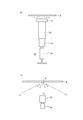
- FIG. 1B is a diagram in which the main part is extracted from FIG. 1A in order to illustrate the irradiation light L 1 irradiated by the ring fiber illumination 51 and the reflected light (scattered light) L 2 . is there.
- the optical system 50 includes a ring fiber illumination 51, a lens barrel 52, a telecentric lens 53, and a light receiving unit 54.
- the light source of the ring fiber illumination 51 is an ultra-high pressure mercury lamp (wavelength range: 369 nm to 692 nm, output: more than 1,000,000 Lux), and a CCD camera is used for the light receiving unit.
- the irradiation light L 1 irradiated by the ring fiber illumination 51 enters the wafer W at about 20 degrees with respect to the wafer surface, and when it collides with a defect D existing on the back surface of the wafer W, scattered light L 2 is generated.
- the light receiving unit 54 receives vertical scattered light from the scattered light L 2 and picks up an image, and captures and records an image having brightness information of the scattered light together with position information of the optical system 50.
- the present inventors examined that the technique described in Patent Document 1 is applied to the inspection of the defect state on the back surface of the epitaxial wafer.
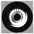
- the technique described in Patent Document 1 is applied to the epitaxial wafer back surface inspection as it is, as shown in an example in FIG. 2, it is impossible to detect almost all defects that can be identified by an appearance inspection.
- almost all of the central portion except the peripheral portion on the back surface of the epitaxial wafer is erroneously recognized as if it is a defect.
- Defects on the back side of the epitaxial wafer include defects that do not cause any problems, such as “pin marks”, “blade scratches”, and “scattering halos” described later. There are also some defects that are made. Therefore, the inspection apparatus for the back side of the epitaxial wafer must be able to correctly identify the type of defect in addition to detecting the presence or absence of the defect and the amount of generation.
- the visual inspection can visually identify the defect on the back surface of the epitaxial wafer and determine its quality.
- the visual inspection requires determination by an inspector. Therefore, establishment of a technique capable of objectively inspecting the back surface of the epitaxial wafer is required.
- an object of the present invention is to provide an epitaxial wafer back surface inspection apparatus capable of detecting defects on the back surface of an epitaxial wafer and an epitaxial wafer back surface inspection method using the same.
- the present inventors diligently studied to achieve the above object.
- the inventors of the present invention have studied the cause of overlooking defects when applied to the backside of an epitaxial wafer, regardless of whether the technique described in Patent Document 1 can correctly evaluate the defect state of a PW wafer.
- the present inventors analyzed the difference between the image on the backside of the epitaxial wafer obtained by the prior art and the defect confirmed by the appearance inspection, the same type or different type of defect overlapped or was a normal part in this image. However, it seems that the brightness information is based on the defect.
- the back surface of the epitaxial wafer has a part of the back surface formed by the wraparound of the source gas compared to the back surface of the PW wafer, and the surface on the back surface side is rough.
- the cause is an overflow of the brightness of scattered light.
- the back surface of the epitaxial wafer is rougher than the PW wafer (that is, the haze level on the back surface is poor), such as when the epitaxial layer is formed, the source gas flows around the back surface and fogging occurs. The above overflow seems to occur. Therefore, even if the technique described in Patent Document 1 is applied to the inspection of the defect state on the back surface of the epitaxial wafer, it is considered that an identifiable defect is overlooked if it is an appearance inspection.
- the front and back surfaces of the PW wafer are less rough, so that when inspecting the PW wafer, even if it is a very thin scratch, it is in a short wavelength region and has high illuminance.
- Ultra high pressure mercury lamps such as lamps and metal halide lamps were used as light sources for ring fiber illumination.
- overflow occurs on the back surface of the epitaxial wafer. Therefore, if the illuminance of the ultra-high pressure mercury lamp is lowered to eliminate this, the illuminance becomes unstable during the inspection.
- the present inventors have conceived of using a light source that can be stably used at a relatively low illuminance as a light source for ring fiber illumination, and found a light source that can identify defects on the back surface of the epitaxial wafer. It came to be completed.
- This invention is based on said knowledge and examination, The summary structure is as follows.
- the epitaxial wafer back surface inspection apparatus of the present invention is installed perpendicularly to the back surface of the epitaxial wafer, an optical system including a ring fiber illumination and a photographing unit, a scanning unit that scans the optical system in parallel with the back surface,
- the light source of the ring fiber illumination is either a blue LED or a red LED.
- the illuminance of the light source is preferably 300,000 Lux or more and 1,000,000 Lux or less, and the light source is preferably the blue LED.
- the epitaxial wafer back surface inspection method of the present invention using the above-described epitaxial wafer back surface inspection apparatus, while scanning the optical system by the scanning unit, continuously shooting the back part images, It has an acquisition process which acquires the whole picture of the back side from the parts image, and a detection process which detects a defect which exists in the back side from the whole picture.
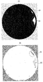
- a defect in a peripheral portion on the back surface of the epitaxial wafer is extracted, and among the defects, the peripheral portion is divided into an inner region and an outer region, the size exceeds a predetermined threshold, and It is preferable that a defect located only in the outer region is detected as a halo.
- a point-like defect is extracted at a peripheral edge of the back surface of the epitaxial wafer, and the point-like defect is not less than a first radius and not more than a second radius, and the center is a dark part. It is preferable to detect a point-like defect as a susceptor pinhole.
- a dot-like reference defect is extracted at a position away from the center of the back surface of the epitaxial wafer by a predetermined distance, and the position of the reference defect is set as a first reference position, and the first reference position is taken from the center.
- One reference position is rotated equiangularly to extract defects in the vicinity of a plurality of second reference positions, and a set of point-like defects in the vicinity of the first reference position and the second reference position is defined by a pin It is preferable to detect it as a mark.
- (A) is a schematic view showing an entire optical system
- (B) is a schematic showing incident light L 1 and the scattered light L 2 FIG.
- (A) is a whole image obtained by the blue LED light source
- (B) is a whole image obtained by the red LED light source
- (C) is a green LED light source.
- (D) is the whole image obtained by the white LED light source. It is a flowchart explaining the epitaxial wafer back surface inspection method according to one Embodiment of this invention. It is a 1st example of the epitaxial wafer back surface obtained by one Embodiment of this invention, (A) is a whole image, (B) image-processes the whole image of (A). It is a schematic diagram for demonstrating the halo which can be detected by one Embodiment of this invention. It is a 2nd example of the epitaxial wafer back surface obtained by one Embodiment of this invention, (A) is a whole image, (B) image-processes the whole image of (A). (A) is an enlarged image of the susceptor pinhole in FIG.
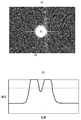
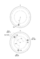
- FIG. 8 (A), and (B) is a graph showing the intensity distribution. It is a schematic diagram for demonstrating the susceptor pinhole which can be detected by one Embodiment of this invention. It is a 3rd example of the epitaxial wafer back surface obtained by one Embodiment of this invention, (A) is a whole image, (B) image-processes the whole image of (A). 4A and 4B are schematic diagrams for explaining pin marks that can be detected according to an embodiment of the present invention, in which (A) shows a reference defect PM1, and (B) shows a set of defects PM1 to PM3 that are pin marks. Show.
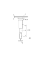
- FIG. 3 is a schematic diagram of epitaxial wafer back surface inspection apparatus 100 according to an embodiment of the present invention.
- an epitaxial wafer back surface inspection apparatus 100 includes a ring fiber illumination 10 and an optical system 30 that are installed perpendicular to the back surface of the epitaxial wafer 1 and an imaging unit 20. And a scanning unit 40 that scans the optical system 30 in parallel with the back surface of the epitaxial wafer 1.
- the light source of the ring fiber illumination 10 is either a blue LED or a red LED.
- the epitaxial wafer 1 is obtained by epitaxially growing an epitaxial layer E on the surface of the substrate S.
- the optical system 30 includes the ring fiber illumination 10 and the imaging unit 20 described above, irradiates the back surface of the epitaxial wafer 1 with the ring fiber illumination 10, receives the scattered light, and acquires a part image of the back surface of the epitaxial wafer 1. To do.
- the scanning unit 40 scans the optical system 30 in parallel with the back surface of the epitaxial wafer 1.
- the scanning unit 40 may scan the optical system 30 in the circumferential direction, or may scan vertically and horizontally.
- the epitaxial wafer back surface inspection apparatus 100 may have a plurality of (for example, three) optical systems 30, and the scanning unit 40 may scan the respective optical systems 30 in the circumferential direction.
- the scanning unit 40 can be composed of an arm connected to the optical system 30, a drive stepping motor for driving the arm, a servo motor, and the like.
- FIG. 4A shows an example when a part image on the back surface of the epitaxial wafer is continuously photographed on the entire surface of the wafer and synthesized to obtain an entire image showing the entire back surface.
- FIG. 4B shows an entire image when the light source is changed from the blue LED to the red LED (irradiation light illuminance: 300,000 to 1,000,000 lux, wavelength range: 600 to 700 nm, emission center wavelength: 660 ⁇ m) on the same back surface. ).
- FIG. 4C shows the entire image when the green LED (light emission center wavelength: 530 ⁇ m) having the same illuminance as those of the blue LED and the red LED is shown in FIG. 4C, and the white LED (the blue LED, the red LED, and the green LED described above).
- FIG. 4D shows an entire image when the combined light is changed to (combined light).
- a scratch-like defect which is an arc-shaped defect, is formed at the center of the entire image shown in FIGS. 4A to 4D, and a blue LED or a red LED is used as the light source.
- a spider defect is formed around the scratch-like defect.
- the scratch-like defect can be identified from the image, but the spider defect seen in FIGS. 4 (A) and 4 (B) cannot be identified.
- the defect detection sensitivity is highest when a blue LED is used as the light source. Therefore, it is preferable to use a blue LED as the light source of the ring fiber illumination 10 of the epitaxial wafer back surface inspection apparatus 100.
- a blue LED or a 600 to 700 nm red LED having excellent stability even at low illuminance and having a wavelength range of 450 to 500 nm is used for the ring fiber illumination 10.
- an image showing the defect state can be accurately obtained even on the back side of an epitaxial wafer having a low haze level. Therefore, it is possible to identify and detect defects on the backside of the epitaxial wafer that could not be detected without visual observation.
- the epitaxial wafer 1 can be an epitaxial silicon wafer obtained by epitaxially growing a silicon epitaxial layer on the surface of a mirror-finished silicon wafer.
- the epitaxial wafer back surface inspection apparatus 100 according to the present embodiment is preferably provided for an epitaxial silicon wafer. This is because the above-described deterioration of the haze on the back side becomes a problem.
- the photographing step S1 first, when the optical system 30 is positioned at a predetermined position, a part image on the back surface of the epitaxial wafer 1 is photographed.
- the scanning unit 40 scans the optical system 30 at a position different from the predetermined position, and takes a part image on the back surface of the epitaxial wafer 1.
- the back surface of the epitaxial wafer 1 is divided into about 100 to 200, and this imaging and scanning are repeated for each division, and the part images on the back surface of the epitaxial wafer 1 are continuously photographed (S1).
- the photographed part images are synthesized to obtain an entire image of the back surface of the epitaxial wafer 1 (S2).
- An example of the obtained whole image is, for example, FIG.
- the detection step S3 Prior to the detection step S3, it is preferable to further include an image processing step for image processing of the acquired entire image. And it is preferable to perform detection process S3 based on the whole image image-processed.
- the image processing step for example, if a differential processing image is acquired from the entire image, the influence of noise and the like can be suppressed, and defects existing on the back surface of the epitaxial wafer 1 can be detected more clearly.
- FIG. 6B is obtained.
- FIGS. 8A and 8B and FIGS. 11A and 11B have the same correspondence.
- FIG. 11A shows an entire image of the back surface of the epitaxial wafer 1 on which the pin marks PM1 to PM3 are formed, obtained using the epitaxial wafer back surface inspection apparatus 100 according to the present invention.
- FIG. 11B is an image process of FIG. 11A.
- the “pin mark” is a slight scratch such as a wear scar generated on the outer peripheral portion of the back surface of the epitaxial wafer, which is unique to the epitaxial furnace manufactured by Centura, due to the shape of the wafer lift pin and the contact condition between the pin and the wafer. It is a defect consisting of an aggregate or a deposit.
- pin marks that can be formed at three locations are always formed at the same time, and in this case, exist at positions rotated by 120 degrees from the center of the back side of the epitaxial wafer. Further, due to the lift pin shape, the pin mark exists within a predetermined radius range, and each pin mark defect becomes a circular bright spot.
Landscapes
- Physics & Mathematics (AREA)
- General Physics & Mathematics (AREA)
- Health & Medical Sciences (AREA)
- Life Sciences & Earth Sciences (AREA)
- Chemical & Material Sciences (AREA)
- Analytical Chemistry (AREA)
- Biochemistry (AREA)
- General Health & Medical Sciences (AREA)
- Immunology (AREA)
- Pathology (AREA)
- Testing Or Measuring Of Semiconductors Or The Like (AREA)
- Investigating Materials By The Use Of Optical Means Adapted For Particular Applications (AREA)
- Length Measuring Devices By Optical Means (AREA)
- Engineering & Computer Science (AREA)
- Manufacturing & Machinery (AREA)
Abstract
Description
図3に示すように、本発明の一実施形態に従うエピタキシャルウェーハ裏面検査装置100は、エピタキシャルウェーハ1の裏面に対して垂直に設置される、リングファイバー照明10および撮影部20を備える光学系30と、エピタキシャルウェーハ1の裏面と平行に光学系30を走査する走査部40と、を有する。そして、リングファイバー照明10の光源を、青色LEDおよび赤色LEDのいずれかとする。なお、図3における、エピタキシャルウェーハ1とは、基板Sの表面にエピタキシャル層Eをエピタキシャル成長させたものである。そして、エピタキシャルウェーハ1の裏面とは、エピタキシャル層Eが形成された側と反対の面(換言すれば、基板Sのエピタキシャル層Eが形成されていない側の面であり、基板Sの裏側の面が露出していると言うこともできる。)を意味する。以下、各構成の詳細を順に説明する。
次に、上述のエピタキシャルウェーハ裏面検査装置100を用いるエピタキシャルウェーハ裏面検査方法の一実施形態を説明する。図5に示すように、本実施形態は、光学系30を走査部40により走査しつつ、エピタキシャルウェーハ1の裏面のパーツ画像を連続的に撮影する撮影工程S1と、前記パーツ画像から、エピタキシャルウェーハ1の裏面の全体画像を取得する取得工程S2と、得られた全体画像から、エピタキシャルウェーハ1の裏面に存在する欠陥を検出する検出工程S3と、を有する。
欠陥の第1の例として、図6(A)に、本発明に従うエピタキシャルウェーハ裏面検査装置100を用いて取得した、ハローD1が形成されているエピタキシャルウェーハ1裏面の全体画像を示す。また、図6(B)は、図6(A)を画像処理したものである。なお、このエピタキシャルウェーハ1裏面にはクモリ欠陥D2も形成されている。
ここで、「ハロー」とは、エピタキシャル成長によってエピタキシャルウェーハ裏面の周縁部に発生するエッチング模様状の欠陥である。
欠陥の第2の例として、図8(A)に、本発明に従うエピタキシャルウェーハ裏面検査装置100を用いて取得した、サセプタピンホールD3が形成されているエピタキシャルウェーハ1裏面の全体画像を示す。また、図8(B)は、図8(A)を画像処理したものである。さらに、図9(A)に図8(A)におけるサセプタピンホールD3近傍の拡大画像を示す。また、図9(B)に、このサセプタピンホールD3の強度(輝度)分布を示す。図9(A),(B)に一具体例が示されているように、サセプタピンホールは略円形の点状の欠陥であって、中央部は暗部となる。
ここで、「サセプタピンホール」とは、エピタキシャル成長中にサセプタによるピンホールがエピタキシャルウェーハの裏面に転写された痕跡であり、核を持ったくもり状に目視される欠陥である。そのため、サセプタピンホールの外径は、所定の範囲内となる。
欠陥の第3の例として、図11(A)に、本発明に従うエピタキシャルウェーハ裏面検査装置100を用いて取得した、ピンマークPM1~PM3が形成されているエピタキシャルウェーハ1裏面の全体画像を示す。また、図11(B)は、図11(A)を画像処理したものである。
ここで、「ピンマーク」とは、ウェーハリフトピン形状や、ピンとウェーハとの接触具合に起因し、センチュラ社製のエピタキシャル炉に特有な、エピタキシャルウェーハ裏面外周部に発生する摩耗跡のような微少キズの集合体または付着物からなる欠陥である。ウェーハリフトピン形状にも依るが、例えば3箇所に形成されうるピンマークであれば、必ず3箇所同時に形成され、この場合、エピタキシャルウェーハ裏面の中心から120度ずつ回転させた位置に存在する。また、リフトピン形状に起因して、所定の半径の範囲内にピンマークは存在し、ピンマークそれぞれの欠陥は円形状の輝点となる。
10 リングファイバー照明
20 撮影部
30 光学系
40 走査部
100 エピタキシャルウェーハ裏面検査装置
D 欠陥
Claims (9)
- エピタキシャルウェーハの裏面に対して垂直に設置される、リングファイバー照明および撮影部を備える光学系と、
前記裏面と平行に前記光学系を走査する走査部と、を有し、
前記リングファイバー照明の光源は、青色LEDおよび赤色LEDのいずれかであることを特徴とするエピタキシャルウェーハ裏面検査装置。 - 前記光源の照度は300,000Lux以上1,000,000Lux以下である、請求項1に記載のエピタキシャルウェーハ裏面検査装置。
- 前記光源は、前記青色LEDである、請求項1または2に記載のエピタキシャルウェーハ裏面検査装置。
- 請求項1~3のいずれか1項に記載のエピタキシャルウェーハ裏面検査装置を用いて、前記光学系を前記走査部により走査しつつ、前記裏面のパーツ画像を連続的に撮影する撮影工程と、
前記パーツ画像から、前記裏面の全体画像を取得する取得工程と、
前記全体画像から、前記裏面に存在する欠陥を検出する検出工程と、を有することを特徴とするエピタキシャルウェーハ裏面検査方法。 - 前記検出工程に先立ち、前記全体画像を画像処理する画像処理工程を更に有し、
前記検出工程において、前記画像処理した全体画像に基づき前記検出を行う、請求項4に記載のエピタキシャルウェーハ裏面検査方法。 - 前記検出工程において、前記エピタキシャルウェーハ裏面の周縁部における欠陥を抽出し、前記欠陥のうち、前記周縁部を内側領域および外側領域に区画し、所定の閾値を超える大きさであり、かつ、前記外側領域内のみに位置する欠陥をハローとして検出する、請求項4または5に記載のエピタキシャルウェーハ裏面検査方法。
- 前記検出工程において、前記エピタキシャルウェーハ裏面の周縁部における点状の欠陥を抽出し、前記点状の欠陥のうち、第1の半径以上かつ第2の半径以下であり、かつ、中心が暗部となる点状の欠陥をサセプタピンホールとして検出する、請求項4~6のいずれか1項に記載のエピタキシャルウェーハ裏面検査方法。
- 前記検出工程において、前記エピタキシャルウェーハ裏面の中心から所定の距離離れた位置における点状の規準欠陥を抽出して、該規準欠陥の位置を第1の規準位置とし、前記中心から前記第1の規準位置を等角ずつ回転させて複数の第2の規準位置近傍における欠陥を抽出し、前記第1の規準位置および前記第2の規準位置近傍における点状の欠陥がなす組を、ピンマークとして検出する、請求項4~7のいずれか1項に記載のエピタキシャルウェーハ裏面検査方法。
- 前記抽出した前記欠陥を正常欠陥および異常欠陥に分類し、前記異常欠陥の有無を判定する判定工程を更に有する、請求項4~8のいずれか1項に記載のエピタキシャルウェーハ裏面検査方法。
Priority Applications (4)
| Application Number | Priority Date | Filing Date | Title |
|---|---|---|---|
| US15/765,349 US10338005B2 (en) | 2015-10-05 | 2016-08-03 | Apparatus for inspecting back surface of epitaxial wafer and method of inspecting back surface of epitaxial wafer using the same |
| CN201680058167.0A CN108139339B (zh) | 2015-10-05 | 2016-08-03 | 外延晶片背面检查装置及使用其的外延晶片背面检查方法 |
| KR1020187009499A KR102066520B1 (ko) | 2015-10-05 | 2016-08-03 | 에피택셜 웨이퍼 이면 검사 장치 및 그것을 이용한 에피택셜 웨이퍼 이면 검사 방법 |
| DE112016004547.6T DE112016004547B4 (de) | 2015-10-05 | 2016-08-03 | Vorrichtung zum inspizieren einer hinteren oberfläche eines epitaxialwafers und verfahren zum inspizieren einer hinteren oberfläche eines epitaxialwafers unter verwendung derselben |
Applications Claiming Priority (2)
| Application Number | Priority Date | Filing Date | Title |
|---|---|---|---|
| JP2015-197776 | 2015-10-05 | ||
| JP2015197776A JP6601119B2 (ja) | 2015-10-05 | 2015-10-05 | エピタキシャルウェーハ裏面検査装置およびそれを用いたエピタキシャルウェーハ裏面検査方法 |
Publications (1)
| Publication Number | Publication Date |
|---|---|
| WO2017061063A1 true WO2017061063A1 (ja) | 2017-04-13 |
Family
ID=58487333
Family Applications (1)
| Application Number | Title | Priority Date | Filing Date |
|---|---|---|---|
| PCT/JP2016/003583 Ceased WO2017061063A1 (ja) | 2015-10-05 | 2016-08-03 | エピタキシャルウェーハ裏面検査装置およびそれを用いたエピタキシャルウェーハ裏面検査方法 |
Country Status (7)
| Country | Link |
|---|---|
| US (1) | US10338005B2 (ja) |
| JP (1) | JP6601119B2 (ja) |
| KR (1) | KR102066520B1 (ja) |
| CN (1) | CN108139339B (ja) |
| DE (1) | DE112016004547B4 (ja) |
| TW (1) | TWI627398B (ja) |
| WO (1) | WO2017061063A1 (ja) |
Cited By (1)
| Publication number | Priority date | Publication date | Assignee | Title |
|---|---|---|---|---|
| CN108169247A (zh) * | 2017-12-29 | 2018-06-15 | 星阵(广州)基因科技有限公司 | 一种毛细玻璃管品质检测装置 |
Families Citing this family (9)
| Publication number | Priority date | Publication date | Assignee | Title |
|---|---|---|---|---|
| CN102666135B (zh) * | 2009-11-23 | 2015-12-16 | 米其林集团总公司 | 具有带有用于改善雪地性能的倒角的侧凹槽的轮胎 |
| JP6380582B1 (ja) * | 2017-03-08 | 2018-08-29 | 株式会社Sumco | エピタキシャルウェーハの裏面検査方法、エピタキシャルウェーハ裏面検査装置、エピタキシャル成長装置のリフトピン管理方法およびエピタキシャルウェーハの製造方法 |
| TWI647465B (zh) * | 2017-08-16 | 2019-01-11 | 旺矽科技股份有限公司 | 光學檢測系統 |
| JP6844529B2 (ja) * | 2017-12-27 | 2021-03-17 | 株式会社Sumco | エピタキシャルウェーハの製造方法およびエピタキシャルウェーハ |
| KR102453258B1 (ko) * | 2020-01-15 | 2022-10-11 | 주식회사 커미조아 | 웨이퍼 모서리 결함 검사장치 및 검사방법 |
| CN111307819B (zh) * | 2020-03-16 | 2024-03-08 | 上海华力微电子有限公司 | 晶圆边缘缺陷检测系统及方法 |
| CN115128099A (zh) * | 2022-08-29 | 2022-09-30 | 苏州高视半导体技术有限公司 | 晶圆缺陷检测方法、晶圆缺陷检测设备及其拍摄装置 |
| JP2024176947A (ja) | 2023-06-09 | 2024-12-19 | 株式会社Sumco | 欠陥検出装置、欠陥検出方法、及びプログラム |
| CN117890371B (zh) * | 2024-01-18 | 2024-07-26 | 马鞍山芯乔科技有限公司 | 一种晶圆外观检测功能影像迭合的方法 |
Citations (7)
| Publication number | Priority date | Publication date | Assignee | Title |
|---|---|---|---|---|
| JPS63124942A (ja) * | 1986-11-04 | 1988-05-28 | ワツカー・ケミトロニク・ゲゼルシヤフト・フユア・エレクトロニク・グルントシユトツフエ・ミツト・ベシユレンクテル・ハフツング | 特に半導体スライスの表面性状を測定するための方法と装置 |
| JPH07249665A (ja) * | 1994-03-11 | 1995-09-26 | Komatsu Electron Metals Co Ltd | シリコンウェーハの汚染度評価方法 |
| JP2007067102A (ja) * | 2005-08-30 | 2007-03-15 | Sharp Corp | 多結晶半導体ウエハの外観検査方法および外観検査装置 |
| JP2007292641A (ja) * | 2006-04-26 | 2007-11-08 | Tokyo Seimitsu Co Ltd | 外観検査装置 |
| JP2010103275A (ja) * | 2008-10-23 | 2010-05-06 | Sumco Corp | ウェーハ裏面の評価方法 |
| JP2010127897A (ja) * | 2008-12-01 | 2010-06-10 | Tech Vision:Kk | リング型照明装置 |
| JP2015513111A (ja) * | 2012-04-12 | 2015-04-30 | ケーエルエー−テンカー コーポレイション | サンプル検査とレビューのためのシステム及び方法 |
Family Cites Families (30)
| Publication number | Priority date | Publication date | Assignee | Title |
|---|---|---|---|---|
| JPS57161641A (en) * | 1981-03-31 | 1982-10-05 | Olympus Optical Co Ltd | Inspecting device for defect of surface |
| US4450358A (en) * | 1982-09-22 | 1984-05-22 | Honeywell Inc. | Optical lithographic system |
| JP2941308B2 (ja) * | 1989-07-12 | 1999-08-25 | 株式会社日立製作所 | 検査システムおよび電子デバイスの製造方法 |
| DE4413831C2 (de) | 1994-04-20 | 2000-05-31 | Siemens Ag | Verfahren zur Kontrolle von Halbleiterscheiben |
| US5609780A (en) * | 1994-11-14 | 1997-03-11 | International Business Machines, Corporation | Laser system |
| US6002262A (en) * | 1996-07-19 | 1999-12-14 | Komatsu Electronic Metals Co., Ltd. | Method of and apparatus for measuring flatness of semiconductor wafers that have not been subjected to donor-killer treatment |
| US6503594B2 (en) * | 1997-02-13 | 2003-01-07 | Samsung Electronics Co., Ltd. | Silicon wafers having controlled distribution of defects and slip |
| DE69800328T2 (de) * | 1998-02-05 | 2001-02-01 | Wacker Siltronic Gesellschaft Fuer Halbleitermaterialien Ag | Vorrichtung und Verfahren zur Inspektion der Mikrotextur am Umfang einer Halbleiterscheibe |
| US6700606B1 (en) * | 1999-06-09 | 2004-03-02 | Activcard Ireland Limited | Micromirror optical imager |
| FR2797714B1 (fr) * | 1999-08-20 | 2001-10-26 | Soitec Silicon On Insulator | Procede de traitement de substrats pour la microelectronique et substrats obtenus par ce procede |
| JP2001168160A (ja) * | 1999-12-07 | 2001-06-22 | Sony Corp | 半導体ウェハの検査システム |
| TW502132B (en) * | 2000-08-30 | 2002-09-11 | Toshiba Corp | Method for producing photomask |
| US7049586B2 (en) * | 2002-02-21 | 2006-05-23 | Applied Material Israel, Ltd. | Multi beam scanning with bright/dark field imaging |
| US7016028B2 (en) * | 2002-06-07 | 2006-03-21 | Interuniversitair Microelektronica Centrum (Imec) | Method and apparatus for defect detection |
| US6825487B2 (en) * | 2002-07-30 | 2004-11-30 | Seh America, Inc. | Method for isolation of wafer support-related crystal defects |
| US7968354B1 (en) * | 2002-10-04 | 2011-06-28 | Kla-Tencor Technologies Corp. | Methods for correlating backside and frontside defects detected on a specimen and classification of backside defects |
| KR100553710B1 (ko) * | 2004-03-23 | 2006-02-24 | 삼성전자주식회사 | 반도체 웨이퍼를 검사하는 검사 시스템 및 검사 방법 |
| TWI257140B (en) * | 2004-04-13 | 2006-06-21 | Komatsu Denshi Kinzoku Kk | Semiconductor wafer inspection device and method |
| US7315361B2 (en) * | 2005-04-29 | 2008-01-01 | Gsi Group Corporation | System and method for inspecting wafers in a laser marking system |
| US7583833B2 (en) * | 2006-01-27 | 2009-09-01 | Advanced Micro Devices, Inc. | Method and apparatus for manufacturing data indexing |
| WO2007137261A2 (en) * | 2006-05-22 | 2007-11-29 | Kla-Tencor Technologies Corporation | Methods and systems for detecting pinholes in a film formed on a wafer or for monitoring a thermal process tool |
| US8173449B2 (en) * | 2006-06-09 | 2012-05-08 | Sumco Corporation | Method for making COP evaluation on single-crystal silicon wafer |
| US7754502B1 (en) * | 2006-10-27 | 2010-07-13 | National Semiconductor Corporation | Backside defect detector and method that determines whether unwanted materials are present on the backside of a semiconductor wafer |
| JP5369643B2 (ja) * | 2008-06-10 | 2013-12-18 | 富士通セミコンダクター株式会社 | 欠陥検査装置 |
| JP5332478B2 (ja) | 2008-10-06 | 2013-11-06 | 株式会社Sumco | レーザー散乱式欠陥検査装置及びレーザー散乱式欠陥検査方法 |
| JP2010103261A (ja) * | 2008-10-22 | 2010-05-06 | Toshiba Corp | 半導体評価装置、半導体評価方法及び半導体製造装置 |
| KR101089787B1 (ko) * | 2009-12-15 | 2011-12-07 | 한국생산기술연구원 | 포토루미네선스 이미징을 이용한 led 에피웨이퍼 검사 장치 및 그 방법 |
| US9031810B2 (en) * | 2011-01-11 | 2015-05-12 | Haiguang Chen | Methods and systems of object based metrology for advanced wafer surface nanotopography |
| JP5682858B2 (ja) * | 2011-05-20 | 2015-03-11 | 株式会社Sumco | シリコンウェーハの評価方法および製造方法 |
| JP6004033B1 (ja) * | 2015-04-14 | 2016-10-05 | 株式会社Sumco | エピタキシャルウェーハの評価方法および評価装置 |
-
2015
- 2015-10-05 JP JP2015197776A patent/JP6601119B2/ja active Active
-
2016
- 2016-08-03 KR KR1020187009499A patent/KR102066520B1/ko active Active
- 2016-08-03 CN CN201680058167.0A patent/CN108139339B/zh active Active
- 2016-08-03 DE DE112016004547.6T patent/DE112016004547B4/de active Active
- 2016-08-03 WO PCT/JP2016/003583 patent/WO2017061063A1/ja not_active Ceased
- 2016-08-03 US US15/765,349 patent/US10338005B2/en active Active
- 2016-08-10 TW TW105125394A patent/TWI627398B/zh active
Patent Citations (7)
| Publication number | Priority date | Publication date | Assignee | Title |
|---|---|---|---|---|
| JPS63124942A (ja) * | 1986-11-04 | 1988-05-28 | ワツカー・ケミトロニク・ゲゼルシヤフト・フユア・エレクトロニク・グルントシユトツフエ・ミツト・ベシユレンクテル・ハフツング | 特に半導体スライスの表面性状を測定するための方法と装置 |
| JPH07249665A (ja) * | 1994-03-11 | 1995-09-26 | Komatsu Electron Metals Co Ltd | シリコンウェーハの汚染度評価方法 |
| JP2007067102A (ja) * | 2005-08-30 | 2007-03-15 | Sharp Corp | 多結晶半導体ウエハの外観検査方法および外観検査装置 |
| JP2007292641A (ja) * | 2006-04-26 | 2007-11-08 | Tokyo Seimitsu Co Ltd | 外観検査装置 |
| JP2010103275A (ja) * | 2008-10-23 | 2010-05-06 | Sumco Corp | ウェーハ裏面の評価方法 |
| JP2010127897A (ja) * | 2008-12-01 | 2010-06-10 | Tech Vision:Kk | リング型照明装置 |
| JP2015513111A (ja) * | 2012-04-12 | 2015-04-30 | ケーエルエー−テンカー コーポレイション | サンプル検査とレビューのためのシステム及び方法 |
Cited By (2)
| Publication number | Priority date | Publication date | Assignee | Title |
|---|---|---|---|---|
| CN108169247A (zh) * | 2017-12-29 | 2018-06-15 | 星阵(广州)基因科技有限公司 | 一种毛细玻璃管品质检测装置 |
| CN108169247B (zh) * | 2017-12-29 | 2023-12-01 | 星阵(广州)基因科技有限公司 | 一种毛细玻璃管品质检测装置 |
Also Published As
| Publication number | Publication date |
|---|---|
| KR20180050369A (ko) | 2018-05-14 |
| CN108139339A (zh) | 2018-06-08 |
| TW201719150A (zh) | 2017-06-01 |
| TWI627398B (zh) | 2018-06-21 |
| JP2017072403A (ja) | 2017-04-13 |
| US10338005B2 (en) | 2019-07-02 |
| CN108139339B (zh) | 2020-10-16 |
| KR102066520B1 (ko) | 2020-01-15 |
| JP6601119B2 (ja) | 2019-11-06 |
| US20180306731A1 (en) | 2018-10-25 |
| DE112016004547B4 (de) | 2024-07-18 |
| DE112016004547T5 (de) | 2018-06-14 |
Similar Documents
| Publication | Publication Date | Title |
|---|---|---|
| JP6601119B2 (ja) | エピタキシャルウェーハ裏面検査装置およびそれを用いたエピタキシャルウェーハ裏面検査方法 | |
| JP6380582B1 (ja) | エピタキシャルウェーハの裏面検査方法、エピタキシャルウェーハ裏面検査装置、エピタキシャル成長装置のリフトピン管理方法およびエピタキシャルウェーハの製造方法 | |
| JP6531579B2 (ja) | ウェーハ検査方法およびウェーハ検査装置 | |
| TWI617800B (zh) | 磊晶晶圓表面檢查裝置及使用該裝置之磊晶晶圓表面檢查方法 | |
| JP5868203B2 (ja) | 検査装置 | |
| TWI765380B (zh) | 矽晶圓的缺陷檢查方法及矽晶圓的缺陷檢查系統 | |
| JP2005214980A (ja) | ウエハのマクロ検査方法および自動ウエハマクロ検査装置 | |
| JP6493136B2 (ja) | ウェーハ検査方法およびウェーハ検査装置 | |
| JP7400667B2 (ja) | シリコンウェーハの検査方法、シリコンウェーハの製造方法 | |
| KR101880398B1 (ko) | 기판의 얼룩 검사 장치 및 검사 방법 | |
| JP2025159971A (ja) | 半導体ウェーハの評価方法 | |
| JP2008180601A (ja) | 基板端面検査装置 | |
| TW202501655A (zh) | 缺陷檢測設備、缺陷檢測方法、以及程式 |
Legal Events
| Date | Code | Title | Description |
|---|---|---|---|
| 121 | Ep: the epo has been informed by wipo that ep was designated in this application |
Ref document number: 16853222 Country of ref document: EP Kind code of ref document: A1 |
|
| WWE | Wipo information: entry into national phase |
Ref document number: 15765349 Country of ref document: US |
|
| ENP | Entry into the national phase |
Ref document number: 20187009499 Country of ref document: KR Kind code of ref document: A |
|
| WWE | Wipo information: entry into national phase |
Ref document number: 112016004547 Country of ref document: DE |
|
| 122 | Ep: pct application non-entry in european phase |
Ref document number: 16853222 Country of ref document: EP Kind code of ref document: A1 |