WO2017056636A1 - 研磨方法および研磨装置 - Google Patents
研磨方法および研磨装置 Download PDFInfo
- Publication number
- WO2017056636A1 WO2017056636A1 PCT/JP2016/070654 JP2016070654W WO2017056636A1 WO 2017056636 A1 WO2017056636 A1 WO 2017056636A1 JP 2016070654 W JP2016070654 W JP 2016070654W WO 2017056636 A1 WO2017056636 A1 WO 2017056636A1
- Authority
- WO
- WIPO (PCT)
- Prior art keywords
- polishing
- region
- film thickness
- substrate
- wafer
- Prior art date
- Legal status (The legal status is an assumption and is not a legal conclusion. Google has not performed a legal analysis and makes no representation as to the accuracy of the status listed.)
- Ceased
Links
Images




















Classifications
-
- B—PERFORMING OPERATIONS; TRANSPORTING
- B24—GRINDING; POLISHING
- B24B—MACHINES, DEVICES, OR PROCESSES FOR GRINDING OR POLISHING; DRESSING OR CONDITIONING OF ABRADING SURFACES; FEEDING OF GRINDING, POLISHING, OR LAPPING AGENTS
- B24B37/00—Lapping machines or devices; Accessories
- B24B37/005—Control means for lapping machines or devices
-
- B—PERFORMING OPERATIONS; TRANSPORTING
- B24—GRINDING; POLISHING
- B24B—MACHINES, DEVICES, OR PROCESSES FOR GRINDING OR POLISHING; DRESSING OR CONDITIONING OF ABRADING SURFACES; FEEDING OF GRINDING, POLISHING, OR LAPPING AGENTS
- B24B37/00—Lapping machines or devices; Accessories
- B24B37/005—Control means for lapping machines or devices
- B24B37/013—Devices or means for detecting lapping completion
-
- B—PERFORMING OPERATIONS; TRANSPORTING
- B24—GRINDING; POLISHING
- B24B—MACHINES, DEVICES, OR PROCESSES FOR GRINDING OR POLISHING; DRESSING OR CONDITIONING OF ABRADING SURFACES; FEEDING OF GRINDING, POLISHING, OR LAPPING AGENTS
- B24B37/00—Lapping machines or devices; Accessories
- B24B37/04—Lapping machines or devices; Accessories designed for working plane surfaces
- B24B37/042—Lapping machines or devices; Accessories designed for working plane surfaces operating processes therefor
-
- B—PERFORMING OPERATIONS; TRANSPORTING
- B24—GRINDING; POLISHING
- B24B—MACHINES, DEVICES, OR PROCESSES FOR GRINDING OR POLISHING; DRESSING OR CONDITIONING OF ABRADING SURFACES; FEEDING OF GRINDING, POLISHING, OR LAPPING AGENTS
- B24B37/00—Lapping machines or devices; Accessories
- B24B37/04—Lapping machines or devices; Accessories designed for working plane surfaces
- B24B37/07—Lapping machines or devices; Accessories designed for working plane surfaces characterised by the movement of the work or lapping tool
- B24B37/10—Lapping machines or devices; Accessories designed for working plane surfaces characterised by the movement of the work or lapping tool for single side lapping
- B24B37/105—Lapping machines or devices; Accessories designed for working plane surfaces characterised by the movement of the work or lapping tool for single side lapping the workpieces or work carriers being actively moved by a drive, e.g. in a combined rotary and translatory movement
- B24B37/107—Lapping machines or devices; Accessories designed for working plane surfaces characterised by the movement of the work or lapping tool for single side lapping the workpieces or work carriers being actively moved by a drive, e.g. in a combined rotary and translatory movement in a rotary movement only, about an axis being stationary during lapping
-
- B—PERFORMING OPERATIONS; TRANSPORTING
- B24—GRINDING; POLISHING
- B24B—MACHINES, DEVICES, OR PROCESSES FOR GRINDING OR POLISHING; DRESSING OR CONDITIONING OF ABRADING SURFACES; FEEDING OF GRINDING, POLISHING, OR LAPPING AGENTS
- B24B37/00—Lapping machines or devices; Accessories
- B24B37/27—Work carriers
- B24B37/30—Work carriers for single side lapping of plane surfaces
-
- B—PERFORMING OPERATIONS; TRANSPORTING
- B24—GRINDING; POLISHING
- B24B—MACHINES, DEVICES, OR PROCESSES FOR GRINDING OR POLISHING; DRESSING OR CONDITIONING OF ABRADING SURFACES; FEEDING OF GRINDING, POLISHING, OR LAPPING AGENTS
- B24B37/00—Lapping machines or devices; Accessories
- B24B37/27—Work carriers
- B24B37/30—Work carriers for single side lapping of plane surfaces
- B24B37/32—Retaining rings
-
- B—PERFORMING OPERATIONS; TRANSPORTING
- B24—GRINDING; POLISHING
- B24B—MACHINES, DEVICES, OR PROCESSES FOR GRINDING OR POLISHING; DRESSING OR CONDITIONING OF ABRADING SURFACES; FEEDING OF GRINDING, POLISHING, OR LAPPING AGENTS
- B24B37/00—Lapping machines or devices; Accessories
- B24B37/34—Accessories
-
- B—PERFORMING OPERATIONS; TRANSPORTING
- B24—GRINDING; POLISHING
- B24B—MACHINES, DEVICES, OR PROCESSES FOR GRINDING OR POLISHING; DRESSING OR CONDITIONING OF ABRADING SURFACES; FEEDING OF GRINDING, POLISHING, OR LAPPING AGENTS
- B24B49/00—Measuring or gauging equipment for controlling the feed movement of the grinding tool or work; Arrangements of indicating or measuring equipment, e.g. for indicating the start of the grinding operation
- B24B49/02—Measuring or gauging equipment for controlling the feed movement of the grinding tool or work; Arrangements of indicating or measuring equipment, e.g. for indicating the start of the grinding operation according to the instantaneous size and required size of the workpiece acted upon, the measuring or gauging being continuous or intermittent
- B24B49/04—Measuring or gauging equipment for controlling the feed movement of the grinding tool or work; Arrangements of indicating or measuring equipment, e.g. for indicating the start of the grinding operation according to the instantaneous size and required size of the workpiece acted upon, the measuring or gauging being continuous or intermittent involving measurement of the workpiece at the place of grinding during grinding operation
-
- B—PERFORMING OPERATIONS; TRANSPORTING
- B24—GRINDING; POLISHING
- B24B—MACHINES, DEVICES, OR PROCESSES FOR GRINDING OR POLISHING; DRESSING OR CONDITIONING OF ABRADING SURFACES; FEEDING OF GRINDING, POLISHING, OR LAPPING AGENTS
- B24B49/00—Measuring or gauging equipment for controlling the feed movement of the grinding tool or work; Arrangements of indicating or measuring equipment, e.g. for indicating the start of the grinding operation
- B24B49/10—Measuring or gauging equipment for controlling the feed movement of the grinding tool or work; Arrangements of indicating or measuring equipment, e.g. for indicating the start of the grinding operation involving electrical means
- B24B49/105—Measuring or gauging equipment for controlling the feed movement of the grinding tool or work; Arrangements of indicating or measuring equipment, e.g. for indicating the start of the grinding operation involving electrical means using eddy currents
-
- B—PERFORMING OPERATIONS; TRANSPORTING
- B24—GRINDING; POLISHING
- B24B—MACHINES, DEVICES, OR PROCESSES FOR GRINDING OR POLISHING; DRESSING OR CONDITIONING OF ABRADING SURFACES; FEEDING OF GRINDING, POLISHING, OR LAPPING AGENTS
- B24B49/00—Measuring or gauging equipment for controlling the feed movement of the grinding tool or work; Arrangements of indicating or measuring equipment, e.g. for indicating the start of the grinding operation
- B24B49/12—Measuring or gauging equipment for controlling the feed movement of the grinding tool or work; Arrangements of indicating or measuring equipment, e.g. for indicating the start of the grinding operation involving optical means
-
- H—ELECTRICITY
- H10—SEMICONDUCTOR DEVICES; ELECTRIC SOLID-STATE DEVICES NOT OTHERWISE PROVIDED FOR
- H10P—GENERIC PROCESSES OR APPARATUS FOR THE MANUFACTURE OR TREATMENT OF DEVICES COVERED BY CLASS H10
- H10P52/00—Grinding, lapping or polishing of wafers, substrates or parts of devices
-
- H—ELECTRICITY
- H10—SEMICONDUCTOR DEVICES; ELECTRIC SOLID-STATE DEVICES NOT OTHERWISE PROVIDED FOR
- H10P—GENERIC PROCESSES OR APPARATUS FOR THE MANUFACTURE OR TREATMENT OF DEVICES COVERED BY CLASS H10
- H10P52/00—Grinding, lapping or polishing of wafers, substrates or parts of devices
- H10P52/40—Chemomechanical polishing [CMP]
- H10P52/402—Chemomechanical polishing [CMP] of semiconductor materials
-
- H—ELECTRICITY
- H10—SEMICONDUCTOR DEVICES; ELECTRIC SOLID-STATE DEVICES NOT OTHERWISE PROVIDED FOR
- H10P—GENERIC PROCESSES OR APPARATUS FOR THE MANUFACTURE OR TREATMENT OF DEVICES COVERED BY CLASS H10
- H10P74/00—Testing or measuring during manufacture or treatment of wafers, substrates or devices
- H10P74/23—Testing or measuring during manufacture or treatment of wafers, substrates or devices characterised by multiple measurements, corrections, marking or sorting processes
-
- H—ELECTRICITY
- H10—SEMICONDUCTOR DEVICES; ELECTRIC SOLID-STATE DEVICES NOT OTHERWISE PROVIDED FOR
- H10P—GENERIC PROCESSES OR APPARATUS FOR THE MANUFACTURE OR TREATMENT OF DEVICES COVERED BY CLASS H10
- H10P74/00—Testing or measuring during manufacture or treatment of wafers, substrates or devices
- H10P74/23—Testing or measuring during manufacture or treatment of wafers, substrates or devices characterised by multiple measurements, corrections, marking or sorting processes
- H10P74/238—Testing or measuring during manufacture or treatment of wafers, substrates or devices characterised by multiple measurements, corrections, marking or sorting processes comprising acting in response to an ongoing measurement without interruption of processing, e.g. endpoint detection or in-situ thickness measurement
-
- H—ELECTRICITY
- H10—SEMICONDUCTOR DEVICES; ELECTRIC SOLID-STATE DEVICES NOT OTHERWISE PROVIDED FOR
- H10P—GENERIC PROCESSES OR APPARATUS FOR THE MANUFACTURE OR TREATMENT OF DEVICES COVERED BY CLASS H10
- H10P74/00—Testing or measuring during manufacture or treatment of wafers, substrates or devices
- H10P74/20—Testing or measuring during manufacture or treatment of wafers, substrates or devices characterised by the properties tested or measured, e.g. structural or electrical properties
- H10P74/203—Structural properties, e.g. testing or measuring thicknesses, line widths, warpage, bond strengths or physical defects
Definitions
- the present invention relates to a polishing method and a polishing apparatus for polishing a surface of a substrate such as a wafer, and more particularly to a method and an apparatus for polishing a surface of a substrate having a variation in film thickness along the circumferential direction of the substrate.
- CMP Chemical mechanical polishing
- the process of forming a film on the wafer is performed using various film forming techniques such as plating, chemical vapor deposition (CVD), and physical vapor deposition (PVD).
- a film may not be formed uniformly over the entire surface of the wafer.
- the film thickness may vary along the circumferential direction of the wafer, or the entire film may be formed obliquely.
- the film thickness distribution may differ between the wafers.
- the conventional CMP technique has not been able to eliminate such variations in film thickness along the circumferential direction of the wafer.
- the present invention can eliminate variations in film thickness along the circumferential direction of a substrate such as a wafer, and can provide the same film thickness distribution among a plurality of substrates regardless of the difference in film thickness distribution.
- An object of the present invention is to provide a polishing apparatus.
- a film thickness distribution in a circumferential direction of a substrate is acquired, and a first film having a largest film thickness or a smallest film thickness is obtained based on the film thickness distribution.
- the surface of the substrate is pressed against the polishing pad while rotating the substrate with a polishing head, and the first region is moved within the surface of the substrate.
- the polishing method is characterized by polishing at a removal rate different from the removal rate of the second region.
- the first region and the second region are symmetric with respect to the center of the substrate.
- the step of pressing the surface of the substrate against the polishing pad increases the distance of the first region from the rotation center line of the polishing head while rotating the substrate with the polishing head.
- the step of polishing the first region at a removal rate different from the removal rate of the second region in the surface of the substrate is the first region in the radial direction of the polishing table. Is positioned outside the second region, the first region is placed within the surface of the substrate by increasing or decreasing the load applied from the polishing head to the entire surface of the substrate. It is a process of polishing at a removal rate different from the removal rate of the second region.
- the step of polishing the first region at a removal rate different from the removal rate of the second region in the surface of the substrate is the first region in the radial direction of the polishing table. Is positioned outside the second region, the first region is changed to the second region by increasing or decreasing a local load applied from the polishing head to the first region. It is a step of polishing at a removal rate different from the removal rate of the region. In a preferred aspect of the present invention, the step of polishing the first region at a removal rate different from the removal rate of the second region in the surface of the substrate is the first region in the radial direction of the polishing table.
- the polishing head When the polishing head is located outside the second region, the polishing head is moved outwardly or inwardly in the radial direction of the polishing table together with the substrate, whereby the first region is moved to the second region. It is a step of polishing at a removal rate different from the removal rate of the region.
- the step of pressing the surface of the substrate against the polishing pad is performed by rotating the substrate with the polishing head and tilting a film holder that holds the elastic film of the polishing head.
- the step of pressing the surface of the substrate against the polishing pad is characterized in that the film holder is inclined upward or downward from the first region toward the second region.
- a film thickness distribution in a circumferential direction of a substrate is acquired, a first region having the largest or smallest film thickness is determined based on the film thickness distribution, and the substrate While rotating the substrate stage holding the substrate, the polishing disk is pressed against the surface of the substrate while rotating the polishing disk, and the first area is different from the removal rate of the second area in the surface of the substrate.
- a polishing method characterized by polishing at a removal rate.
- the first region and the second region are symmetric with respect to the center of the substrate.
- the step of polishing the first region at a removal rate different from the removal rate of the second region in the surface of the substrate is such that the polishing disk is in contact with the first region.
- the first region is polished at a removal rate different from the removal rate of the second region in the surface of the substrate by increasing the relative speed between the first region and the polishing disk. It is a process to perform.
- the step of polishing the first region at a removal rate different from the removal rate of the second region in the surface of the substrate is such that the polishing disk is in contact with the first region. In this case, the first region is polished at a removal rate different from the removal rate of the second region in the surface of the substrate by increasing the load of the polishing disk.
- a first film thickness distribution indicating a film thickness distribution in the circumferential direction of a substrate is obtained, and a first film having the largest or smallest film thickness is obtained based on the first film thickness distribution.
- the surface of the substrate is pressed against the polishing pad while rotating the substrate with a polishing head, and the first region is moved within the surface of the substrate.
- Performing a first stage polishing step of polishing at a removal rate different from the removal rate of the second region obtaining a second film thickness distribution indicating a film thickness distribution in the circumferential direction of the polished substrate, 2.
- the third region having the largest or smallest film thickness is determined, the substrate stage holding the substrate is rotated, and the polishing disk is rotated while the polishing disk is rotated.
- the removal rate of the fourth region within the surface of the substrate is a polishing method which comprises carrying out the second-stage polishing step of polishing at different removal rates.
- the first region and the second region are symmetric with respect to the center of the substrate, and the third region and the fourth region are symmetric with respect to the center of the substrate. It is characterized by that.
- Another aspect of the present invention includes a polishing table that supports a polishing pad, a polishing head that presses a substrate against the polishing pad, a head rotation motor that rotates the polishing head around a rotation center line, and the polishing head.
- a polishing apparatus including a head eccentric mechanism that is eccentric with respect to a rotation center line.
- the head eccentric mechanism causes the polishing head to be eccentric in a direction in which the distance of the first region in the surface of the substrate from the rotation center line of the polishing head increases or decreases.
- the polishing head can polish the first region at a removal rate different from the removal rate of the second region in the surface of the substrate.
- the first region and the second region are symmetric with respect to the center of the substrate.
- Another aspect of the present invention includes a polishing table that supports a polishing pad, and a polishing head that presses a substrate against the polishing pad.
- the polishing head includes a head body, and an elastic film that presses the substrate against the polishing pad.
- a film holder for holding the elastic film, at least three partition walls forming at least three working chambers between the head body and the film holder, and pressures in the at least three working chambers independently.
- a polishing apparatus comprising: at least three pressure regulators capable of tilting the film holder in a desired direction by controlling.
- the film holder is inclined upward or downward from the first region in the surface of the substrate toward the second region, so that the polishing head has the first region.
- the first region and the second region are symmetric with respect to the center of the substrate.
- the difference in film thickness between the first region and the second region can be reduced by polishing the first region at a removal rate different from that of the second region.
- the film thicknesses in the first region and the second region can be the same. Therefore, the polishing method according to the present invention can eliminate variations in film thickness along the circumferential direction of the substrate.
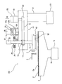
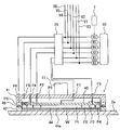
- FIG. 1 is a perspective view showing an embodiment of a CMP (Chemical Mechanical Polishing) apparatus. It is a figure which shows the detailed structure of CMP apparatus. It is sectional drawing of a grinding
- CMP Chemical Mechanical Polishing
- FIG. 30 is a cross-sectional view taken along line AA in FIG. 29.
- 1 is a perspective view illustrating one embodiment of a buffing apparatus that can be used to finish polish the entire surface of a substrate such as a wafer.
- FIG. 35A is a diagram illustrating a state in which only the first film thickness sensor operates to measure the film thickness of the wafer.
- FIG. 35B is a diagram illustrating a state in which only the first film thickness sensor operates and the film thickness of the wafer is measured.
- FIG. 36A is a diagram illustrating a state in which only the second film thickness sensor operates to measure the film thickness of the wafer.
- 36B is a diagram illustrating a state in which only the second film thickness sensor operates to measure the film thickness of the wafer. It is a figure which shows the movement path
- FIG. It is a top view when the grinding
- CMP chemical mechanical polish
- FIG. 1 is a perspective view showing an embodiment of a CMP (Chemical Mechanical Polishing) apparatus which is a main polishing apparatus for chemically and mechanically polishing the entire surface of a substrate such as a wafer.
- a CMP apparatus 100 as a main polishing apparatus supplies a slurry to a polishing head (substrate holding apparatus) 1 that holds and rotates a wafer W that is an example of a substrate, a polishing table 3 that supports a polishing pad 2, and a polishing pad 2.
- the slurry supply nozzle 5 is provided.
- the upper surface of the polishing pad 2 constitutes a polishing surface 2a for polishing the wafer W.
- the polishing head 1 is configured to hold the wafer W on the lower surface thereof by vacuum suction.
- the polishing head 1 presses the wafer W against the polishing surface 2 a of the polishing pad 2 while the polishing head 1 and the polishing table 3 rotate in the same direction as indicated by arrows.
- the polishing surface 2a is larger than the surface of the wafer W, and the entire surface of the wafer W is pressed against the polishing surface 2a.
- Slurry is supplied from the slurry supply nozzle 5 onto the polishing pad 2, and the wafer W is brought into sliding contact with the polishing surface 2a of the polishing pad 2 in the presence of the slurry.
- the surface of the wafer W is polished by a combined effect of a mechanical action by abrasive grains contained in the slurry and a chemical action by chemical components of the slurry.
- the polishing table 3 is provided with one or more film thickness sensors 15 for measuring the film thickness of the wafer W.
- the film thickness sensor 15 is an eddy current sensor or an optical sensor, and is configured to output a film thickness index value that changes according to the film thickness of the wafer W.
- the film thickness index value is a value that directly or indirectly indicates the film thickness.
- the film thickness sensor 15 rotates together with the polishing table 3. Each time the polishing table 3 rotates once, the film thickness sensor 15 measures the film thickness at a plurality of measurement points including the center of the wafer W, and outputs the above-described film thickness index value.
- the film thickness sensor 15 is connected to the data processing unit 6. Film thickness index values obtained at a plurality of measurement points on the surface of the wafer W are sent to the data processing unit 6 as film thickness data.
- the data processing unit 6 creates a film thickness profile from the film thickness data, and further creates a film thickness distribution from the film thickness profile.
- the film thickness profile indicates the relationship between the film thickness index value (that is, the film thickness) and the radial position on the wafer W, and the film thickness distribution indicates the film thickness index value in the circumferential direction of the wafer W. (That is, the film thickness distribution).
- the data processing unit 6 is connected to the operation control unit 7.
- the operation controller 7 determines polishing conditions based on the film thickness distribution. More specifically, the operation control unit 7 determines a polishing condition for bringing the current film thickness distribution closer to the target film thickness distribution.
- the operation control unit 7 is connected to the polishing condition adjustment system 8 and is configured to control the operation of the polishing condition adjustment system 8.
- the polishing condition adjusting system 8 includes a pressure regulator, a head turning motor, a head eccentric mechanism, and the like which will be described later.
- FIG. 2 is a diagram showing a detailed configuration of the CMP apparatus 100.
- the polishing table 3 is connected to a table motor 13 arranged below the table shaft 3a, and is rotatable around the table shaft 3a.
- a polishing pad 2 is attached to the upper surface of the polishing table 3.
- the table motor 13 constitutes a polishing surface moving mechanism that moves the polishing surface 2a in the horizontal direction.
- the polishing head 1 is connected to a head shaft 11, and the head shaft 11 moves up and down with respect to the head arm 16 by a vertical movement mechanism 27. By moving the head shaft 11 up and down, the entire polishing head 1 is moved up and down with respect to the head arm 16 for positioning.
- a rotary joint 25 is attached to the upper end of the head shaft 11.
- a vertical movement mechanism 27 that moves the head shaft 11 and the polishing head 1 up and down is supported by a bridge 28 that rotatably supports the head shaft 11 via a bearing 26, a ball screw 32 attached to the bridge 28, and a support 30. And a servo motor 38 provided on the support base 29.
- a support base 29 that supports the servo motor 38 is fixed to the head arm 16 via a support column 30.
- the ball screw 32 includes a screw shaft 32a connected to the servo motor 38 and a nut 32b into which the screw shaft 32a is screwed.
- the head shaft 11 moves up and down integrally with the bridge 28. Therefore, when the servo motor 38 is driven, the bridge 28 moves up and down via the ball screw 32, and thereby the head shaft 11 and the polishing head 1 move up and down.
- the head shaft 11 is connected to the rotary cylinder 12 via a key (not shown).
- the rotary cylinder 12 has a timing pulley 14 on the outer periphery thereof.
- a head rotation motor 18 is fixed to the head arm 16, and the timing pulley 14 is connected to a timing pulley 20 provided in the head rotation motor 18 via a timing belt 19. Therefore, the rotary cylinder 12 and the head shaft 11 rotate integrally through the timing pulley 20, the timing belt 19, and the timing pulley 14 by rotating the head rotation motor 18, and the polishing head 1 is centered on its axis. Rotate.
- the head rotation motor 18, the timing pulley 20, the timing belt 19, and the timing pulley 14 constitute a polishing head rotation mechanism that rotates the polishing head 1 about its axis.
- the head arm 16 is supported by a head arm shaft 21 that is rotatably supported by a frame (not shown).
- a rotary encoder 22 as a rotation angle detector is attached to the head rotation motor 18.
- the rotary encoder 22 is configured to detect the rotation angle of the polishing head 1 connected to the head rotation motor 18.
- the rotary encoder 22 is connected to the data processing unit 6 shown in FIG. 1, and the rotation angle of the polishing head 1 detected by the rotary encoder 22 is transmitted to the data processing unit 6.
- the polishing head 1 is configured to hold a substrate such as a wafer W on the lower surface thereof.
- the head arm 16 is configured to be pivotable about a head arm shaft 21, and the head arm shaft 21 is connected to a head pivot motor 23.
- the head turning motor 23 is configured to be able to rotate the head arm shaft 21 clockwise and counterclockwise by a predetermined angle. Therefore, when the head turning motor 23 is operated, the polishing head 1 and the head arm 16 are turned around the head arm shaft 21.
- the polishing of the wafer W is performed as follows.
- the polishing head 1 holding the wafer W on the lower surface is moved from the receiving position of the wafer W to the upper position of the polishing table 3 by turning the head arm 16.
- Each of the polishing head 1 and the polishing table 3 is rotated, and slurry is supplied onto the polishing pad 2 from a slurry supply nozzle 5 provided above the polishing table 3.
- the polishing head 1 is lowered, and the wafer W is pressed against the polishing surface 2 a of the polishing pad 2.
- the wafer W is brought into sliding contact with the polishing surface 2a of the polishing pad 2 to polish the surface of the wafer W.
- FIG. 3 is a cross-sectional view of the polishing head 1.
- the polishing head 1 includes a head main body 41 connected to the head shaft 11, and a retainer ring 42 disposed below the head main body 41.
- an elastic film 44 that contacts the upper surface of the wafer W (the surface opposite to the surface to be polished) and a film holder 45 that holds the elastic film 44 are disposed.
- the elastic film 44 has a wafer contact surface (substrate contact surface) 44 a that contacts the upper surface of the wafer W.
- the wafer contact surface (substrate contact surface) 44 a is circular, and the wafer W can be pressed against the polishing surface 2 a of the polishing pad 2.
- the pressure chambers P 1, P 2, P 3 and P 4 are formed by the elastic film 44 and the film holder 45.
- the central pressure chamber P1 is circular, and the other pressure chambers P2, P3, P4 are annular. These pressure chambers P1, P2, P3, and P4 are arranged concentrically.
- Pressurized gas such as pressurized air is supplied to the pressure chambers P1, P2, P3, and P4 by a gas supply source 50 through gas transfer lines F1, F2, F3, and F4, respectively.
- vacuum lines V1, V2, V3, and V4 are connected to the gas transfer lines F1, F2, F3, and F4, and negative pressure is applied to the pressure chambers P1, P2, P3, and P4 by the vacuum lines V1, V2, V3, and V4. Pressure is formed.
- the internal pressures of the pressure chambers P1, P2, P3, P4 can be changed independently of each other, so that the corresponding four regions of the wafer W, that is, the central part, the inner intermediate part, the outer intermediate part, In addition, the polishing pressure for the peripheral edge can be adjusted independently.
- a pressure chamber P5 is formed between the membrane holder 45 and the head main body 41, and pressurized gas is supplied to the pressure chamber P5 by the gas supply source 50 via a gas transfer line F5. .
- a vacuum line V5 is connected to the gas transfer line F5, and a negative pressure is formed in the pressure chamber P5 by the vacuum line V5.
- the peripheral edge of the wafer W is surrounded by a retainer ring 42 so that the wafer W does not jump out of the polishing head 1 during polishing.
- An opening is formed in a portion of the elastic film 44 constituting the pressure chamber P3, and the wafer W is attracted and held by the polishing head 1 by forming a vacuum in the pressure chamber P3. Further, the wafer W is released from the polishing head 1 by supplying nitrogen gas, clean air, or the like to the pressure chamber P3.
- An annular rolling diaphragm 46 is disposed between the head body 41 and the retainer ring 42, and a pressure chamber P6 is formed inside the rolling diaphragm 46.
- the pressure chamber P6 is connected to the gas supply source 50 through a gas transfer line F6.
- the gas supply source 50 supplies pressurized gas into the pressure chamber P ⁇ b> 6, thereby pressing the retainer ring 42 against the polishing pad 2.
- a vacuum line V6 is connected to the gas transfer line F6, and a negative pressure is formed in the pressure chamber P6 by the vacuum line V6.
- Pressure regulators R1, R2, R3, R4, R5, R6 are provided in the gas transfer lines F1, F2, F3, F4, F5, F6 communicating with the pressure chambers P1, P2, P3, P4, P5, P6, respectively. ing.
- the pressurized gas from the gas supply source 50 is supplied into the pressure chambers P1 to P6 through the pressure regulators R1 to R6.
- the pressure regulators R1 to R6 are connected to the pressure chambers P1 to P6 by gas transfer lines F1 to F6.
- the gas transfer lines F1 to F6 extend from the pressure chambers P1 to P6 to the gas supply source 50 via the rotary joint 25 and the pressure regulators R1 to R6.
- the pressure regulators R1 to R6 control the pressure in the pressure chambers P1 to P6 by adjusting the pressure of the pressurized gas supplied from the gas supply source 50.
- the pressure regulators R1 to R6 are connected to the operation control unit 7 shown in FIG.
- the pressure chambers P1 to P6 are also connected to an atmosphere release valve (not shown), and the pressure chambers P1 to P6 can be opened to the atmosphere.
- the operation control unit 7 sets the target pressure values of the pressure chambers P1 to P4 based on the film thickness profile and the film thickness distribution generated from the film thickness data, and the target pressures corresponding to the pressures in the pressure chambers P1 to P4 are set.
- the pressure regulators R1 to R4 are operated so that the values are maintained. Since the pressure chambers P1 to P4 are arranged concentrically, the film thickness variation along the radial direction of the wafer W can be eliminated, but the film thickness variation along the circumferential direction of the wafer W is eliminated. I can't do it.
- the CMP apparatus 100 as the main polishing apparatus eliminates the variation in film thickness along the circumferential direction of the wafer W as follows. First, before the wafer W is polished, an associating process for associating the orientation of the wafer W with the rotation angle of the polishing head 1 is performed. This association step is performed using a notch detection sensor 51 that detects notches (notches) formed in the peripheral edge of the wafer W.
- the notch detection sensor 51 is disposed beside the polishing table 3.
- the polishing head 1 holds the wafer W, and the polishing head 1 is moved by the head turning motor 23 until the peripheral edge of the wafer W is positioned above the notch detection sensor 51.
- the notch (notch) 53 of the wafer W is detected by the notch detection sensor 51 while the polishing head 1 and the wafer W rotate around the axis of the polishing head 1.
- the rotation angle of the polishing head 1 (that is, the rotation angle of the wafer W) is measured by the rotary encoder 22 shown in FIG. 2, and the measured value of the rotation angle of the polishing head 1 is transmitted to the data processing unit 6.
- the notch detection sensor 51 is connected to the data processing unit 6, and an output signal of the notch detection sensor 51 is transmitted to the data processing unit 6.
- FIG. 5 is a graph showing the relationship between the output signal of the notch detection sensor 51 and the rotation angle of the polishing head 1.
- the data processing unit 6 can acquire the relationship between the output signal of the notch detection sensor 51 and the rotation angle of the polishing head 1 as shown in FIG.
- the data processing unit 6 determines the rotation angle of the polishing head 1 that represents the position of the notch 53 based on the change in the output signal of the notch detection sensor 51.
- the output signal of the notch detection sensor 51 changes greatly when the rotation angle of the polishing head 1 is 180 degrees. Therefore, the data processing unit 6 determines that the rotation angle of the polishing head 1 representing the position of the notch 53 is 180 degrees.
- the data processing unit 6 can represent the orientation of the wafer W by the rotation angle of the polishing head 1.
- the notch detection sensor 51 can be composed of an eddy current sensor, an optical sensor, an image sensor, or the like.
- the film thickness sensor 15 disposed on the polishing table 3 can also be used as a notch detection sensor. In this case, it is not necessary to provide the notch detection sensor 51 beside the polishing table 3.
- FIG. 6 is a diagram showing an embodiment in which the film thickness sensor 15 arranged on the polishing table 3 is used as a cutout detection sensor.
- the polishing table 3 is rotated until the film thickness sensor 15 reaches a predetermined position.
- This predetermined position is a position where the film thickness sensor 15 faces the peripheral edge of the wafer W held by the polishing head 1 when the polishing head 1 is at the polishing position shown in FIG.
- the polishing head 1 holding the wafer W is moved to a position immediately above the polishing position shown in FIG. At this position, the polishing head 1 and the wafer W are not in contact with the polishing pad 2.
- the notch (notch) 53 of the wafer W is detected by the film thickness sensor 15 as the notch detection sensor while the polishing head 1 and the wafer W rotate about the axis of the polishing head 1. Also in the method shown in FIG. 6, the data processing unit 6 can acquire the relationship between the output signal of the film thickness sensor 15 as the notch detection sensor and the rotation angle of the polishing head 1 as shown in FIG. 5. .
- a profile acquisition process for acquiring the film thickness profile of the wafer is performed.
- the polishing head 1 presses the surface (lower surface) of the wafer W against the polishing surface 2a of the polishing pad 2 with a low load while rotating the polishing table 3 and the polishing head 1 at different rotational speeds. This is done by measuring the film thickness at a plurality of measurement points on the surface of the wafer W by the sensor 15.
- the plurality of measurement points on the surface of the wafer W preferably includes the center of the wafer W.
- the initial film thickness profile is the initial film thickness profile.
- the load of the polishing head 1 when the surface (lower surface) of the wafer W is pressed against the polishing pad 2 is a load that is low enough that the polishing of the wafer W does not proceed substantially.
- the film thickness profile is acquired by causing the film thickness sensor 15 to cross the surface of the wafer W only once.
- the film thickness sensor 15 measures the film thickness at a plurality of measurement points including the center of the wafer W, and sends the film thickness index value to the data processing unit 6.
- the data processing unit 6 creates a film thickness profile as shown in FIG. 8 from the film thickness index value.
- This film thickness profile shows the relationship between the film thickness index value and the position in the radial direction on the surface of the wafer W.
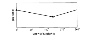
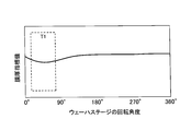
- FIG. 7 is a graph of film thickness distribution showing the relationship between the rotation angle of the polishing head 1 and the corresponding film thickness index value. As can be seen from the film thickness distribution shown in FIG. 10, the film thickness index value when the rotation angle of the polishing head 1 is 0 ° is the largest.
- the film thickness sensor 15 is caused to traverse the surface of the wafer W a plurality of times, thereby obtaining a film thickness profile. get.
- the film thickness sensor 15 measures the film thickness at a plurality of measurement points including the center of the wafer W every time the polishing table 3 rotates, and sends the film thickness index value to the data processing unit 6.
- the data processing unit 6 creates a film thickness profile as shown in FIG. 12 from the film thickness index value.
- FIG. 13 is a data table showing the relationship between the rotation angle of the polishing head 1 and the corresponding film thickness index value for each rotation of the polishing table 3
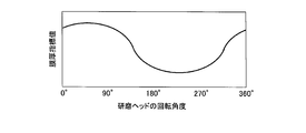
- FIG. 14 shows the rotation of the polishing head 1 shown in FIG. It is a graph which shows the relationship between an angle and a corresponding film thickness index value. As can be seen from FIG. 14, the film thickness index value when the rotation angle of the polishing head 1 is 45 ° is the largest.
- the data processing unit 6 creates a film thickness distribution in the circumferential direction of the wafer W from the film thickness profile obtained as described above, and based on this film thickness distribution, the film thickness of the wafer W is the largest, or A first region including the smallest part is determined.
- the first region can be specified by the rotation angle of the polishing head 1.
- the first region where the film thickness of the wafer W is the largest is the position where the polishing head 1 has a rotation angle of 0 °.
- the first region where the film thickness of the wafer W is the largest is the position where the rotation angle of the polishing head 1 is 45 °.
- the operation control unit 7 determines the polishing conditions so that the film thicknesses in the first region and the second region symmetrical with respect to the center of the wafer W are equal.
- the second area is a comparison area that is automatically specified according to the position of the first area, and is an arbitrary area that satisfies the condition that the first area and the second area are symmetrical with respect to the center of the wafer W. is there.
- the first region is a target region including the largest or smallest film thickness of the wafer W, and has a film thickness different from the film thickness in the second region.
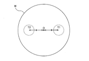
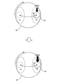
- FIG. 15 is a schematic diagram illustrating an example of the first region and the second region of the wafer W
- FIG. 16 is a schematic diagram illustrating another example of the first region and the second region of the wafer W. is there.
- the first region T ⁇ b> 1 and the second region T ⁇ b> 2 are in the surface to be polished of the wafer W, and are arranged along the circumferential direction of the wafer W.
- the first region T1 and the second region T2 are symmetric with respect to the center O of the wafer W. That is, the distance from the center O of the wafer W to the first region T1 is equal to the distance from the center O of the wafer W to the second region T2.
- the radial position of the first region T1 on the surface of the wafer W can be determined from the film thickness profile shown in FIG. 8 or 12, and the circumferential direction of the first region T1 on the surface of the wafer W can be determined.
- the position can be determined from the film thickness distribution shown in FIG. 10 or FIG.
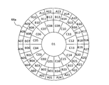
- the position of the first region T1 is represented by using a predefined coordinate region on the wafer contact surface 44a (see FIG. 3) of the polishing head 1. This coordinate area is an area defined on polar coordinates with the center of the wafer contact surface 44a as the origin.
- FIG. 17 is a diagram showing a coordinate area defined in advance on the wafer contact surface 44 a (see FIG. 3) of the polishing head 1. As shown in FIG.
- the coordinate area includes a plurality of areas arranged in the radial direction of the wafer contact surface 44a according to the positions of the four concentric pressure chambers P1, P2, P3, P4 (see FIG. 3) of the polishing head 1. And a plurality of regions arranged in the circumferential direction of the wafer contact surface 44a.
- the polishing head 1 may have only a single pressure chamber.
- the coordinate area defined in advance on the wafer contact surface 44a of the polishing head 1 includes a region aligned in the circumferential direction of the wafer contact surface 44a. Does not include the area aligned in the direction.
- the operation control unit 7 specifies the position of the first region determined by the data processing unit 6 by the coordinate region, and the removal rate of the first region is higher or lower than the removal rate of the second region.
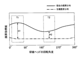
- the polishing conditions are determined so that FIG. 19 is a graph showing an example of the current film thickness distribution and the target film thickness distribution.
- the first region T1 includes a portion having the largest film thickness. Therefore, the difference H1 between the current film thickness distribution and the target film thickness distribution in the first region T1 is larger than the difference H2 between the current film thickness distribution and the target film thickness distribution in the second region T2. Therefore, by polishing the first region T1 at a removal rate higher than that of the second region T2, the first region T1 and the second region T2 can simultaneously approach the target film thickness.
- the difference between the current film thickness distribution and the target film thickness distribution corresponds to the target polishing amount.
- FIG. 20 is a graph showing another example of the current film thickness distribution and the target film thickness distribution.
- the first region T1 includes a portion having the smallest film thickness. Therefore, the difference H1 between the current film thickness distribution and the target film thickness distribution in the first region T1 is smaller than the difference H2 between the current film thickness distribution and the target film thickness distribution in the second region T2. Therefore, by polishing the first region T1 at a removal rate lower than that of the second region T2, the first region T1 and the second region T2 can simultaneously approach the target film thickness.
- polishing head 1 rotates the wafer W
- the polishing head 1 is decentered in a direction in which the distance of the first region from the rotation center line of the polishing head 1 increases.
- the surface of the wafer W is pressed against the polishing pad 2.
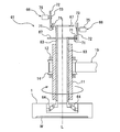
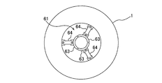
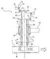
- FIG. 21 is a cross-sectional view showing a head eccentric mechanism 61 that can decenter the polishing head 1 from the rotation center line
- FIG. 22 is a plan view of the head eccentric mechanism 61 shown in FIG. 21 and 22, the polishing head 1 is schematically drawn.
- the head eccentric mechanism 61 is engaged with the inner surface of the head shaft 11, rotates with the head shaft 11, and slides in the vertical direction.
- the rod 63 has a substantially arc-shaped horizontal cross section, and the rods 63.
- Three universal joints 64 respectively connected to the polishing head 1 and three elevating devices 66 for raising and lowering the three rods 63 independently are provided. However, in FIG. 21, only two rods 63, two universal joints 64, and two lifting devices 66 are shown.
- a cylindrical guide member (not shown) that slides with the arc-shaped inner surfaces of the three rods 63 may be provided on the center side of the head shaft 11.
- the three rods 63 and the three universal joints 64 are arranged at equal intervals around the rotation center line L of the polishing head 1.
- Each rod 63 extends in the vertical direction, and an annular disk 67 is fixed to the upper end of each rod 63.
- the circular disk 67 is concentric with the rotation center line L of the polishing head 1.
- the three rods 63 and the three circular disks 67 fixed to the three rods 63 rotate around the rotation center line L together with the polishing head 1, but the positions of the three lifting devices 66 are fixed. Yes.
- the lifting device 66 includes two rollers 71 that are in rolling contact with the upper and lower surfaces of the annular disk 67, a rack 72 that holds these rollers 71, a pinion 73 that meshes with the teeth of the rack 72, and a servo motor that rotates the pinion 73. 75.
- the rack 72 extends in the vertical direction.
- the rotation of the servo motor 75 is converted into a vertical movement by the rack 72 and the pinion 73.
- the pinion 73 rotates and the rack 72 moves in the vertical direction, and the annular disk 67 and the rod 63 move in the vertical direction.
- the roller 71 can move the annular disk 67 and the rod 63 in the vertical direction while allowing the annular disk 67 and the rod 63 to rotate.
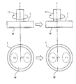
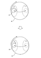
- the vertical movement of the rod 63 is converted into a horizontal movement of the polishing head 1 by the universal joint 64. More specifically, as shown in FIG. 23 and FIG. 24, when one or two of the three rods 63 are raised and the remaining rods 63 are lowered at the same time, the polishing head 1 moves to the rotation center line. Eccentric with respect to L. The direction and amount of the eccentricity of the polishing head 1 can be changed by the vertical displacement of the three rods 63.
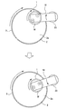
- FIG. 25 is a schematic diagram showing a state where the polishing head 1 is eccentric in the direction in which the distance from the rotation center line L of the first region T1 in the surface of the wafer W increases.
- the distance from the rotation center line L of the first region T1 is longer than the distance from the rotation center line L of the second region T2. Accordingly, the first region T1 moves on the polishing surface 2a of the polishing pad 2 at a higher speed than the second region T2.
- the first region T1 is polished at a removal rate higher than the removal rate of the second region T2.
- the first region T1 and the first region T1 are polished by polishing the first region T1 at a removal rate lower than the removal rate of the second region T2.
- the second region T2 can simultaneously approach the target film thickness. Therefore, in this case, the polishing is performed in a state where the polishing head 1 is decentered in the direction in which the distance of the first region T1 from the rotation center line L of the polishing head 1 is reduced while the wafer W is rotated by the polishing head 1.
- the surface of the wafer W is pressed against the polishing pad 2 with the head 1. Since the distance from the rotation center line L of the first region T1 is shorter than the distance from the rotation center line L of the second region T2, the first region T1 is higher than the removal rate of the second region T2. Polished at a low removal rate.
- FIG. 26 is a schematic diagram showing the wafer W pressed against the polishing surface 2 a of the polishing pad 2 on the polishing table 3.
- the polishing table 3 and the wafer W rotate in the same direction.
- the first region T1 and the second region T2 that are symmetric with respect to the center of the wafer W alternately approach the center of the polishing table 3 and leave.
- the polishing head 1 can polish the first region T1 at a higher removal rate than the removal rate of the second region T2.
- the first region T1 and the first region T1 are polished by polishing the first region T1 at a removal rate lower than the removal rate of the second region T2.
- the second region T2 can simultaneously approach the target film thickness. Therefore, in this case, when the first region T1 is located outside the second region T2 in the radial direction of the polishing table 3, the load applied from the polishing head 1 to the entire surface of the wafer W is reduced. Let By such an operation, the first region T1 is polished at a removal rate lower than the removal rate of the second region T2.
- FIG. 27 is a schematic diagram showing the wafer W pressed against the polishing surface 2 a of the polishing pad 2 on the polishing table 3.
- the polishing table 3 and the wafer W rotate in the same direction.
- the first region T1 and the second region T2 that are symmetric with respect to the center of the wafer W alternately approach the center of the polishing table 3 and leave.
- the polishing head 1 adds the first region T1 to the first region T1 of the wafer W. Increase the local load that is generated. More specifically, when the first region T1 is located outside the second region T2, among the pressure chambers P1, P2, P3, and P4 (see FIG. 3) of the polishing head 1, When the pressure in the one or more pressure chambers at a position corresponding to the position of the first region T1 is increased and the first region T1 is located inside the second region T2, the first The pressure in one or a plurality of pressure chambers at a position corresponding to the position of the region T1 is reduced.
- the polishing head 1 can polish the first region T1 at a higher removal rate than the removal rate of the second region T2.
- the first region T1 and the first region T1 are polished by polishing the first region T1 at a removal rate lower than the removal rate of the second region T2.
- the second region T2 can simultaneously approach the target film thickness. Therefore, in this case, when the first region T1 is positioned outside the second region T2 in the radial direction of the polishing table 3, the polishing head 1 adds the first region T1 to the first region T1 of the wafer W. Reduce local load. By such an operation, the first region T1 is polished at a removal rate lower than the removal rate of the second region T2.
- FIG. 28 is a schematic diagram showing the wafer W pressed against the polishing surface 2 a of the polishing pad 2 on the polishing table 3.
- the polishing table 3 and the wafer W rotate in the same direction. The greater the distance from the center of the polishing table 3 to a certain area in the surface of the wafer W, the higher the relative speed between that area and the polishing surface 2a of the polishing pad 2.
- the polishing head 1 when the first region T1 is positioned outside the second region T2 in the radial direction of the polishing table 3, the polishing head 1 is moved together with the wafer W in the radial direction of the polishing table 3. Move outward. More specifically, when the first region T1 is located outside the second region T2, the head turning motor 23 is operated to move the polishing head 1 and the head arm 16 radially outward. Then, when the first region T1 is located inside the second region T2, the head turning motor 23 is operated to move the polishing head 1 and the head arm 16 radially inward. As described above, by periodically swinging the polishing head 1 and the wafer W according to the rotation of the wafer W, the removal rate of the specific first region T1 can be increased. Therefore, the polishing head 1 can polish the first region T1 at a higher removal rate than the removal rate of the second region T2.
- the first region T1 and the first region T1 are polished by polishing the first region T1 at a removal rate lower than the removal rate of the second region T2.
- the second region T2 can simultaneously approach the target film thickness. Therefore, in this case, when the first region T1 is positioned outside the second region T2 in the radial direction of the polishing table 3, the polishing head 1 is moved inward in the radial direction of the polishing table 3 together with the wafer W. Move to. By such an operation, the first region T1 is polished at a removal rate lower than the removal rate of the second region T2.
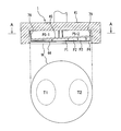
- FIG. 29 is a cross-sectional view of the polishing head 1 used in this embodiment
- FIG. 30 is a cross-sectional view taken along line AA of FIG.
- the polishing head 1 shown in FIGS. 29 and 30 is schematically drawn, and the detailed structure of the polishing head 1 is the same as the structure shown in FIG.
- the surface of the wafer W is polished by the elastic film 44 of the polishing head 1 while the film holder 45 holding the elastic film 44 of the polishing head 1 is tilted while the wafer W is rotated by the polishing head 1.
- Press 2 The film holder 45 is inclined upward from the first region T1 toward the second region T2.
- the partition films 79 are arranged between the head body 41 and the film holder 45.
- the upper ends of the partition films 79 are connected to the inner surface of the head body 41, and the lower ends of the partition films 79 are connected to the upper surface of the film holder 45.
- the partition film 79, the head main body 41, and the film holder 45 form three working chambers P5-1, P5-2, and P5-3.
- the three partition films 79 are arranged at equal intervals around the axis of the polishing head 1. Therefore, the three working chambers P5-1, P5-2, and P5-3 are also arranged at equal intervals around the axis of the polishing head 1. Note that four or more partition walls and four or more working chambers may be provided.
- Pressure regulators R5-1, R5-2, and R5-3 are provided in the gas transfer lines F5-1, F5-2, and F5-3 communicating with the working chambers P5-1, P5-2, and P5-3, respectively. ing.
- the pressurized gas from the gas supply source 50 is supplied into the working chambers P5-1, P5-2, and P5-3 through the pressure regulators R5-1, R5-2, and R5-3.
- the pressure regulators R5-1, R5-2, and R5-3 are connected to the working chambers P5-1, P5-2, and P5-3 by gas transfer lines F5-1, F5-2, and F5-3.
- the gas transfer lines F5-1, F5-2, and F5-3 pass from the working chambers P5-1, P5-2, and P5-3 through the rotary joint 25 and the pressure regulators R5-1, R5-2, and R5-3. Extending to the gas supply source 50.
- the pressure regulators R5-1, R5-2, and R5-3 adjust the pressure of the pressurized gas supplied from the gas supply source 50 to adjust the pressure in the working chambers P5-1, P5-2, and P5-3.
- the pressure regulators R5-1, R5-2, and R5-3 are connected to the operation control unit 7 shown in FIG.
- the working chambers P5-1, P5-2, and P5-3 are also connected to an atmosphere release valve (not shown), and the working chambers P5-1, P5-2, and P5-3 can be opened to the atmosphere. is there.
- vacuum lines V5-1, V5-2, and V5-3 are connected to the gas transfer lines F5-1, F5-2, and F5-3, and the vacuum lines V5-1, V5-2, and V5-3 are connected. As a result, a negative pressure is formed in the working chambers P5-1, P5-2, and P5-3.
- the pressure regulators R5-1, R5-2, and R5-3 can change the internal pressures of the working chambers P5-1, P5-2, and P5-3 independently of each other. By changing the pressure balance in the working chambers P5-1, P5-2, and P5-3, the membrane holder 45 can be tilted in a desired direction.
- the film holder 45 is inclined upward from the first region T1 toward the second region T2.
- the elastic film 44 contracts around the first region T1, while the elastic film 44 extends around the second region T2.
- the polishing head 1 can press the first region T1 with a load larger than the load applied to the second region T2.
- the first region T1 is polished at a higher removal rate than the removal rate of the second region T2.
- the first region T1 and the first region T1 are polished by polishing the first region T1 at a removal rate lower than the removal rate of the second region T2.
- the second region T2 can simultaneously approach the target film thickness. Therefore, in this case, the membrane holder 45 is tilted downward from the first region T1 toward the second region T2 by changing the pressure balance in the working chambers P5-1, P5-2, and P5-3. . By such an operation, the first region T1 is polished at a removal rate lower than the removal rate of the second region T2.
- the film thickness distribution of the wafer W changes as the polishing of the wafer W progresses. For this reason, the position of the first region T1 can also change. Therefore, while the data processing unit 6 updates the film thickness distribution during polishing of the wafer W, the operation control unit 7 may optimize the polishing conditions based on the updated film thickness distribution. For example, every time the polishing table 3 rotates a predetermined number of times (for example, 5 rotations) during polishing of the wafer W, the data processing unit 6 acquires and updates the film thickness distribution, and the operation control unit 7 is updated. The polishing conditions are optimized based on the film thickness distribution. The film thickness distribution during polishing of the wafer W is acquired according to the steps shown in FIGS. 7 to 10 or the steps shown in FIGS.
- the operation control unit 7 optimizes the polishing conditions every time the film thickness distribution is updated, and operates the polishing condition adjustment system 8 according to the optimized polishing conditions. Is polished under optimized polishing conditions.
- the polishing condition adjusting system 8 includes the pressure regulators R1 to R4, the head turning motor 23, the head eccentric mechanism 61, the pressure regulators R5-1, R5-2, and R5-3.
- the first region T1 is symmetric with respect to the center of the wafer by polishing the first region T1 at a different removal rate from the second region T2 based on the difference in film thickness.
- the film thicknesses in the region T1 and the second region T2 can be made the same. Therefore, variations in film thickness along the circumferential direction of the wafer can be eliminated.
- FIG. 31 is a perspective view illustrating one embodiment of a buffing apparatus that can be used to finish polish the entire surface of a substrate such as a wafer.
- the buff polishing apparatus 200 is executed by the buff polishing apparatus 200.
- the buff polishing apparatus 200 includes a wafer stage (substrate stage) 85 that holds the wafer W, a polishing disk 87 that polishes the wafer W on the wafer stage 85, and two film thickness sensors 88 that measure the film thickness of the wafer W. 89.
- the wafer W is placed on the wafer stage 85 with the surface to be polished facing upward.
- the wafer stage 85 is configured to hold the wafer W on its upper surface by vacuum suction.
- the wafer stage 85 is connected to a stage motor 92 via a stage shaft 91, and the wafer stage 85 and the wafer W held by the wafer stage 85 are rotated by the stage motor 92 about the axis of the wafer W.
- a rotary encoder 95 that is a rotation angle detector is attached to the stage motor 92.
- the rotary encoder 95 is configured to detect the rotation angle of the wafer stage 85 connected to the stage motor 92.
- the rotary encoder 95 is connected to the data processing unit 110, and the rotation angle of the wafer stage 85 detected by the rotary encoder 95 is transmitted to the data processing unit 110.
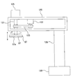
- FIG. 32 is a view showing the polishing disc 87 and the disc arm 120.
- the polishing disc 87 is fixed to the lower end of the disc shaft 121, and this disc shaft 121 is rotatably supported by the disc arm 120.
- a disk motor 122 is disposed in the disk arm 120 to rotate the polishing disk 87 about its axis.
- the disk motor 122 is connected to the disk shaft 121 via a torque transmission mechanism 123 including a pulley and a belt.
- the polishing disk 87 has a polishing cloth 97, and the lower surface of the polishing cloth 97 constitutes a polishing surface 97a for buffing the wafer W.
- the disk arm 120 is provided with a disk pressing device 125 connected to the polishing disk 87 via a disk shaft 121.
- the disk pressing device 125 is composed of an air cylinder or the like, and is configured to press the polishing surface 97a of the polishing disk 87 against the upper surface, which is the surface to be polished of the wafer W.
- the disc arm 120 is configured to be rotatable about a disc arm shaft 128, and the disc arm shaft 128 is connected to a disc turning motor 130.
- the disk turning motor 130 is configured to be able to rotate the disk arm shaft 128 clockwise and counterclockwise by a predetermined angle. When the disk turning motor 130 is operated, the polishing disk 87 and the disk arm 120 are turned around the disk arm shaft 128.
- the two film thickness sensors 88 and 89 are composed of a first film thickness sensor 88 and a second film thickness sensor 89, and these two film thickness sensors 88 and 89 have the same configuration.
- the first film thickness sensor 88 and the second film thickness sensor 89 are attached to the tip of the disk arm 120 and are arranged on both sides of the polishing disk 87. These film thickness sensors 88 and 89 are located above the wafer W held on the wafer stage 85 and measure the film thickness of the wafer W from above the wafer W.
- the first film thickness sensor 88 and the second film thickness sensor 89 are arranged along the moving direction of the polishing disk 87.
- Each of the film thickness sensors 88 and 89 is an eddy current sensor or an optical sensor, and is configured to output a film thickness index value that changes in accordance with the film thickness of the wafer W.
- the film thickness index value is a value that directly or indirectly indicates the film thickness.
- the first film thickness sensor 88 and the second film thickness sensor 89 move together with the polishing disk 87. Each time the polishing disk 87 moves from one end of the wafer W to the other end, the first film thickness sensor 88 and the second film thickness sensor 89 alternately measure the film thickness at a plurality of measurement points including the center of the wafer W. Then, the above-described film thickness index value is output.
- the first film thickness sensor 88 and the second film thickness sensor 89 are connected to the data processing unit 110.
- Film thickness index values obtained at a plurality of measurement points on the surface of the wafer W are sent to the data processing unit 110 as film thickness data.
- the data processing unit 110 creates a film thickness profile from the film thickness data, and further creates a film thickness distribution from the film thickness profile.
- the film thickness profile indicates the relationship between the film thickness index value (that is, the film thickness) and the radial position on the wafer W, and the film thickness distribution indicates the film thickness index value in the circumferential direction of the wafer W. (That is, the film thickness distribution).
- the data processing unit 110 is connected to the operation control unit 112.
- the operation control unit 112 determines the polishing condition based on the film thickness distribution. More specifically, the operation control unit 112 determines a polishing condition for bringing the current film thickness distribution closer to the target film thickness distribution. Further, the operation control unit 112 is connected to the polishing condition adjustment system 113.
- the polishing condition adjustment system 113 is composed of the disk pressing device 125, the disk motor 122, and the like described above.
- the polishing of the wafer W is performed as follows.
- the wafer W is held on a wafer stage (substrate stage) 85 with the surface to be polished facing upward.
- the stage motor 92 rotates the wafer stage 85 and the wafer W, while the disk motor 122 rotates the polishing disk 87.
- the polishing disk 87 is lowered by the disk pressing device 125, and the polishing surface 97 a of the polishing disk 87 is in contact with the surface (upper surface) of the wafer W.
- the polishing disk 87 swings on the surface of the wafer W from one end to the other end a plurality of times.
- the polishing disk 87 is in sliding contact with the surface of the wafer W, thereby polishing the surface of the wafer W.
- the buffing apparatus 200 used as the finish polishing apparatus eliminates the variation in film thickness along the circumferential direction of the wafer W as follows. First, before polishing the wafer W, an associating process for associating the orientation of the wafer W with the rotation angle of the wafer stage 85 is performed. This association step is performed using a first film thickness sensor 88 that functions as a notch detection sensor that detects notches (notches) formed in the peripheral edge of the wafer W.
- FIG. 33 is a diagram illustrating a process of detecting notches formed in the peripheral edge of the wafer W.
- the polishing disk 87 is moved by the disk turning motor 130 until the first film thickness sensor 88 is positioned above the peripheral edge of the wafer W on the wafer stage 85. At this position, the polishing disk 87 is not in contact with the wafer W.
- the notch (notch) of the wafer W is performed by the first film thickness sensor 88 that functions as a notch detection sensor. 53 is detected. During detection of the notch 53, the polishing disk 87 is kept out of contact with the wafer W.
- the rotation angle of the wafer stage 85 (that is, the rotation angle of the wafer W) is measured by the rotary encoder 95 attached to the stage motor 92, and the measurement value of the rotation angle of the wafer stage 85 is transmitted to the data processing unit 110.
- the output signal of the first film thickness sensor 88 is transmitted to the data processing unit 110.
- FIG. 34 is a graph showing the relationship between the output signal of the first film thickness sensor 88 and the rotation angle of the wafer stage 85.
- the data processing unit 110 can acquire the relationship between the output signal of the first film thickness sensor 88 and the rotation angle of the wafer stage 85 as shown in FIG.
- the data processing unit 110 determines the rotation angle of the wafer stage 85 representing the position of the notch 53 based on the change in the output signal of the first film thickness sensor (notch detection sensor) 88.
- the output signal of the first film thickness sensor 88 changes greatly when the rotation angle of the wafer stage 85 is 180 degrees. Therefore, the data processing unit 110 determines that the rotation angle of the wafer stage 85 representing the position of the notch 53 is 180 degrees.
- the data processing unit 110 can represent the orientation of the wafer W by the rotation angle of the wafer stage 85 by using the position of the notch 53 as a reference.
- the second film thickness sensor 89 may be used as a cutout detection sensor.
- a cutout detection sensor may be provided separately from the first film thickness sensor 88 and the second film thickness sensor 89.
- the notch detection sensor can be composed of an eddy current sensor, an optical sensor, an image sensor, or the like.
- a profile acquisition process for acquiring a film thickness profile of the wafer is performed.
- a plurality of film thickness sensors 88 and 89 are used to make a plurality of measurements on the surface of the wafer W while causing the first film thickness sensor 88 and the second film thickness sensor 89 to traverse the surface of the wafer W once or a plurality of times. This is done by measuring the film thickness at the measurement points.
- the plurality of measurement points on the surface of the wafer W preferably includes the center of the wafer W.
- the initial film thickness profile is the initial film thickness profile. While the film thickness index value for creating the initial film thickness profile is acquired, the polishing disk 87 is not in contact with the wafer W, and the wafer W and the wafer stage 85 do not rotate.
- FIG. 35A and FIG. 35B are diagrams showing how only the first film thickness sensor 88 operates to measure the film thickness of the wafer W.
- the first film thickness sensor 88 measures the film thickness at a plurality of measurement points on the surface of the wafer W while traversing the surface of the wafer W. More specifically, the first film thickness sensor 88 starts to move from the edge on one side of the wafer W, and when the second film thickness sensor 89 reaches the edge on the opposite side of the wafer W, The movement of the first film thickness sensor 88 is stopped.
- FIG. 36A and FIG. 36B are diagrams showing a state in which only the second film thickness sensor 89 operates and the film thickness of the wafer W is measured.
- the second film thickness sensor 89 starts to move from the edge on the opposite side of the wafer W, and when the first film thickness sensor 88 reaches the edge on the one side of the wafer W, the second film thickness sensor 89 is moved. The movement of the sensor 89 is stopped. In this way, the first film thickness sensor 88 and the second film thickness sensor 89 alternately measure the film thickness while traversing the surface of the wafer W.
- FIG. 37 is a diagram showing a movement path of the first film thickness sensor 88 and the second film thickness sensor 89.
- symbol J1 represents the movement path of the first film thickness sensor 88
- symbol J2 represents the movement path of the second film thickness sensor 89.
- the data processing unit 110 generates a film thickness profile extending from one edge of the wafer W to the opposite edge. Can do.
- the film thickness is moved while moving one of the first film thickness sensor 88 and the second film thickness sensor 89 from the edge on one side of the wafer W to the edge on the opposite side. May be obtained.
- the film thickness profile may be generated from a film thickness index value acquired while the first film thickness sensor 88 and the second film thickness sensor 89 reciprocate only once on the surface of the wafer W, or the film The thickness profile is generated from the film thickness index value acquired while the first film thickness sensor 88 and the second film thickness sensor 89 are reciprocating on the surface of the wafer W at a plurality of rotation angles of the wafer W. Good.
- the data processing unit 110 creates a film thickness distribution in the circumferential direction of the wafer W from the film thickness profile.
- the generation of the film thickness distribution is performed in the same manner as the steps shown in FIGS. 7 to 10 or the steps shown in FIGS. 11 to 14 in the above-described embodiment, and thus redundant description thereof is omitted.
- the data processing unit 110 determines the first region including the portion with the largest or smallest film thickness of the wafer W.
- the first region can be specified by the rotation angle of the wafer stage 85.
- FIG. 38 is a diagram showing an example of the film thickness distribution.
- the first region T1 is a region including a portion having the largest film thickness, and the first region T1 is a position where the rotation angle of the wafer stage 85 is 45 °.
- FIG. 39 is a diagram showing another example of the film thickness distribution.
- the first region T1 is a region including a portion having the smallest film thickness, and the first region is a position where the rotation angle of the wafer stage 85 is 45 °.
- the operation control unit 112 determines the polishing conditions so that the film thicknesses in the first region and the second region that are symmetrical with respect to the center of the wafer W are equal.
- the second area is a comparison area that is automatically specified according to the position of the first area, and is an arbitrary area that satisfies the condition that the first area and the second area are symmetrical with respect to the center of the wafer W. is there.
- the first region is a target region including the largest or smallest film thickness of the wafer W, and has a film thickness different from the film thickness in the second region. Examples of the first region and the second region include the first region T1 and the second region T2 shown in FIGS. 15 and 16 in the above-described embodiment.
- the radial position of the first region on the surface of the wafer W can be determined from the film thickness profile (see FIGS. 8 and 12), and the circumferential position of the first region on the surface of the wafer W is It can be determined from the film thickness distribution (see FIGS. 38 and 39).
- the position of the first region is represented using a predefined coordinate region on the surface of the wafer W.
- This coordinate area is an area defined on polar coordinates with the center of the wafer W as the origin.
- the coordinate area defined in this embodiment is substantially the same as the coordinate area shown in FIG. That is, the coordinate area includes a plurality of areas arranged in the radial direction of the wafer W and a plurality of areas arranged in the circumferential direction of the wafer W.
- the surface of the wafer W is polished by the polishing disk 87.
- the polishing of the wafer W is performed by swinging the rotating polishing disc 87 on the surface of the wafer W a plurality of times while rotating the wafer W on the wafer stage 85.
- the wafer stage 85 is rotated at a rotation speed higher than the rotation speed of the polishing disk 87.
- the two film thickness sensors 88 and 89 measure the film thickness of the wafer W alternately as described above while swinging with the polishing disc 87, and the film accompanying each rotation angle and swing position.
- the thickness index value is transmitted to the data processing unit 110 as film thickness data.
- the first region is polished at a removal rate different from the removal rate of the second region.
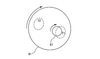
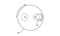
- a polishing method for polishing the first region at a removal rate different from the removal rate of the second region will be described.
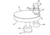
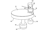
- the relative speed between the first region and the polishing disc 87 is increased.
- the rotational speed of the polishing disk 87 can be changed by a disk motor 122 shown in FIG.
- FIG. 40 is a plan view when the polishing disk 87 is located on one side of the surface of the wafer W
- FIG. 41 is a view when the polishing disk 87 is located on the opposite side of the surface of the wafer W.
- FIG. Under the condition that the wafer stage 85 and the wafer W are rotated at a rotation speed higher than the rotation speed of the polishing disk 87, the rotation speed of the polishing disk 87 is changed when the polishing disk 87 is in contact with the first region T1. Reduce. Further, when the polishing disk 87 is separated from the first region T1, the rotation speed of the polishing disk 87 is increased to approach the rotation speed of the wafer stage 85 and the wafer W.
- the relative speed between the first region and the polishing disk 87 is higher than the relative speed between the second region and the polishing disk 87. In this way, by periodically increasing the relative speed between the polishing disk 87 and the wafer W according to the rotation of the wafer W, the removal rate of the specific first region T1 can be increased. Therefore, the polishing disk 87 can polish the first region T1 at a higher removal rate than the removal rate of the second region T2.
- the rotation speed of the polishing disk 87 is made higher than the rotation speed of the wafer stage 85 and the wafer W, thereby making the first region T1.
- the relative speed of the polishing disk 87 may be increased.
- the polishing disk 87 Under the condition that the wafer stage 85 and the wafer W are rotated at a rotation speed higher than the rotation speed of the polishing disk 87, the polishing disk 87 is in contact with the first region T1, as shown in FIG. , The rotational speed of the polishing disk 87 may be decreased when the position is located inside the first region T1. Further, as shown in FIG. 43, when the polishing disc 87 is in contact with the first region T1 and the polishing disc 87 is positioned outside the first region T1, the rotational speed of the polishing disc 87 is increased. It may be increased. Also by such an operation, the relative speed between the first region T1 and the polishing disk 87 can be increased. Therefore, the polishing disk 87 can polish the first region T1 at a higher removal rate than the removal rate of the second region T2.
- the first region T1 and the first region T1 are polished by polishing the first region T1 at a removal rate lower than the removal rate of the second region T2.
- the second region T2 can simultaneously approach the target film thickness. Therefore, in this case, when the polishing disk 87 is in contact with the first region T1, the rotation speed of the polishing disk 87 is brought close to the rotation speed of the wafer stage 85 and the wafer W, so that the first region T1 The relative speed with the polishing disk 87 can be lowered. Therefore, the polishing disc 87 can polish the first region T1 at a removal rate lower than the removal rate of the second region T2.
- the load of the polishing disk 87 when the polishing disk 87 is in contact with the first region T1 is increased.
- the load of the polishing disc 87 can be changed by a disc pressing device 125 shown in FIG.
- FIG. 44 is a plan view when the polishing disk 87 is located on one side on the surface of the wafer W
- FIG. 45 is a view when the polishing disk 87 is located on the opposite side on the surface of the wafer W.
- FIG. 45 When the polishing disc 87 is in contact with the first region T1, the load on the polishing disc 87 is increased. Further, when the polishing disc 87 is separated from the first region T1, the load on the polishing disc 87 is reduced. The load of the polishing disk 87 when it is in contact with the first region T1 is larger than the load of the polishing disk 87 when it is in contact with the second region T2.
- the polishing disk 87 can polish the first region T1 at a higher removal rate than the removal rate of the second region T2.
- the first region T1 and the first region T1 are polished by polishing the first region T1 at a removal rate lower than the removal rate of the second region T2.
- the second region T2 can simultaneously approach the target film thickness. Therefore, in this case, when the polishing disk 87 is in contact with the first region T1, the load on the polishing disk 87 is reduced. By such an operation, the polishing disk 87 can polish the first region T1 at a removal rate lower than the removal rate of the second region T2.
- the film thickness distribution of the wafer W changes as the polishing of the wafer W progresses. For this reason, the position of the first region T1 can also change. Therefore, while the data processing unit 110 updates the film thickness distribution during polishing of the wafer W, the operation control unit 112 may optimize the polishing conditions based on the updated film thickness distribution. For example, each time the polishing disk 87 reciprocates (swings) on the surface of the wafer W a predetermined number of times (for example, 5 times) during polishing of the wafer W, the data processing unit 110 acquires and updates the film thickness distribution, The operation control unit 112 optimizes the polishing conditions based on the updated film thickness distribution.
- the operation control unit 112 optimizes the polishing conditions every time the film thickness distribution is updated, operates the polishing condition adjustment system 113 according to the optimized polishing conditions, and operates the wafer W. Is polished under optimized polishing conditions.
- the polishing condition adjustment system 113 includes the above-described disk pressing device 125, disk motor 122, and the like.
- the above-described buff polishing apparatus 200 may be used alone for polishing the surface of the wafer, or may be used in combination with the above-described chemical mechanical polishing (CMP) apparatus 100.
- CMP chemical mechanical polishing
- the CMP apparatus 100 is used as a main polishing apparatus for polishing the entire surface of the wafer, and the buffing apparatus 200 is polished by the CMP apparatus 100. Used as a final polishing apparatus for performing final polishing of the surface of a wafer.
- FIG. 46 is a schematic diagram showing a composite polishing system including the chemical mechanical polishing (CMP) apparatus 100 described above and the buff polishing apparatus 200 described above.
- this composite polishing system includes a chemical mechanical polishing (CMP) apparatus 100 as a main polishing apparatus for polishing the entire surface of the wafer, and finish polishing of the surface of the wafer polished by the CMP apparatus 100.
- Buffing apparatus 200 as a final polishing apparatus for performing cleaning, cleaning unit 300 for cleaning the wafer polished by buffing apparatus 200, drying unit 400 for drying the cleaned wafer, and CMP apparatus for the wafer 100, a buffing apparatus 200, a cleaning unit 300, and a transporting apparatus 500 that transports between the drying unit 400.
- the arrangement of the CMP apparatus 100, the buffing apparatus 200, the cleaning unit 300, and the drying unit 400 is not limited to the embodiment shown in FIG. 46, and other arrangements may be applied.
- the CMP apparatus 100 executes a first stage polishing process for polishing the entire surface of the wafer including the first area and the second area described above, and the buff polishing apparatus 200 performs the wafer polishing after the first stage polishing process.
- a second stage polishing step is performed to finish polish the surface.
- FIG. 47 is a flowchart showing an operation sequence of the composite polishing system.
- step 1 the target film thickness distribution of the wafer is input to the operation control unit 7 of the CMP apparatus 100 and stored.
- the wafer to be polished is held by the polishing head 1 of the CMP apparatus 100.
- step 3 the notch position of the wafer is detected, and further, an associating process for associating the orientation of the wafer with the rotation angle of the polishing head 1 is performed (see FIGS. 4 to 6).
- step 4 a first initial film thickness profile indicating the relationship between the initial film thickness index value and the radial position on the wafer is acquired.
- the acquisition of the first initial film thickness profile is performed while pressing the wafer against the polishing pad 2 with a low load. More specifically, the acquisition of the first initial film thickness profile is performed according to the steps shown in FIGS. 7 and 8, or the steps shown in FIG. 11 or FIG.
- a first film thickness distribution indicating a distribution of film thickness index values in the circumferential direction of the wafer (that is, a film thickness distribution) is obtained from the first initial film thickness profile.
- the acquisition of the first film thickness distribution is performed according to the steps shown in FIGS. 9 and 10, or the steps shown in FIG. 13 or FIG.
- step 6 based on the first film thickness distribution, a first region including a portion having the largest or smallest film thickness of the wafer is determined.
- step 7 the polishing conditions are determined so that the film thicknesses in the first region and the second region symmetrical with respect to the center of the wafer are equal.
- the second area is a comparison area that is automatically specified according to the position of the first area, and is an arbitrary area that satisfies the condition that the first area and the second area are symmetric with respect to the center of the wafer. .
- step 8 the first stage polishing process of the wafer is performed under the determined polishing conditions.
- the film thickness profile is continuously acquired, and the first film thickness distribution is updated based on the newly acquired film thickness profile. Further, the polishing conditions are optimized based on the updated first film thickness distribution. As described above, during the polishing of the wafer, the updated first film thickness distribution is fed back to the determination of the polishing conditions.
- step 9 when the first target film thickness distribution is reached, or when a predetermined polishing time is reached, the first stage polishing process of the wafer is ended.
- step 10 the polished wafer is transferred from the CMP apparatus 100 to the buff polishing apparatus 200 by the transfer apparatus 500.
- step 11 the wafer is held on the wafer stage 85 of the buffing apparatus 200 with the polished surface facing upward.
- step 12 the notch position of the wafer is detected, and an associating process for associating the orientation of the wafer with the rotation angle of the wafer stage 85 is performed (see FIGS. 33 and 34).
- a second initial film thickness profile indicating the relationship between the initial film thickness index value and the radial position on the wafer is acquired.
- a second film thickness distribution indicating a distribution of film thickness index values in the circumferential direction of the wafer polished in the first stage polishing process (that is, a film thickness distribution) is obtained from the second initial film thickness profile.
- Acquisition of the second initial film thickness profile and acquisition of the second film thickness distribution are performed in the same manner as the steps shown in FIGS. 7 to 10 or the steps shown in FIGS.
- step 15 based on the second film thickness distribution, a third region including the largest or smallest portion of the wafer film thickness is determined.
- the polishing conditions are determined so that the film thicknesses in the third region and the fourth region that are symmetric with respect to the center of the wafer are equal.
- the fourth area is a comparison area that is automatically specified according to the position of the third area, and is an arbitrary area that satisfies the condition that the third area and the fourth area are symmetric with respect to the center of the wafer. .
- the third region and the fourth region correspond to the first region T1 and the second region T2 described in each embodiment of the buffing apparatus 200 shown in FIGS. 31 to 45, respectively. That is, the third region and the fourth region are symmetric with respect to the center of the wafer W.
- step 17 a second stage polishing process of the wafer is performed under the determined polishing conditions.
- the film thickness profile is continuously acquired, and the second film thickness distribution is updated based on the newly acquired film thickness profile. Further, the polishing conditions are optimized based on the updated second film thickness distribution. As described above, during the polishing of the wafer, the updated second film thickness distribution is fed back to the determination of the polishing conditions.
- step 18 when the second target film thickness distribution is reached or when a predetermined polishing time is reached, the second stage polishing process of the wafer is ended.
- step 19 the polished wafer is transferred from the buffing apparatus 200 to the cleaning unit 300 by the transfer apparatus 500, and the polished wafer is cleaned here.
- step 20 the cleaned wafer is transferred from the cleaning unit 300 to the drying unit 400 by the transfer device 500, and the cleaned wafer is dried here. In this way, a series of wafer processes including a first stage polishing process, a second stage polishing process, a cleaning process, and a drying process are performed.
- the present invention can be used for a method and an apparatus for polishing a surface of a substrate.
- Polishing head (substrate holding device) DESCRIPTION OF SYMBOLS 2 Polishing pad 2a Polishing surface 3 Polishing table 5 Slurry supply nozzle 6 Data processing part 7 Operation control part 8 Polishing condition adjustment system 11 Head shaft 12 Rotary cylinder 13 Table motor 14 Timing pulley 15 Film thickness sensor 16 Head arm 18 Head rotation motor 19 Timing belt 20 Timing pulley 21 Head arm shaft 22 Rotary encoder 25 Rotary joint 26 Bearing 27 Vertical movement mechanism 28 Bridge 29 Support base 30 Support column 32 Ball screw 32a Screw shaft 32b Nut 38 Servo motor 41 Head body 42 Retainer ring 44 Elastic film 44a Wafer Contact surface (substrate contact surface) 45 Film holder 50 Gas supply source 51 Notch detection sensor 53 Notch 61 Head eccentric mechanism 63 Rod 64 Universal joint 66 Lifting device 67 Ring disk 71 Roller 72 Rack 73 Pinion 75 Servo motor 79 Bulkhead film 85 Wafer stage (substrate stage) 87 Polishing discs 88 and 89 Film thickness sensor 91 Stage shaft 92 Stage motor 95 Rotary encoder
Landscapes
- Engineering & Computer Science (AREA)
- Mechanical Engineering (AREA)
- Finish Polishing, Edge Sharpening, And Grinding By Specific Grinding Devices (AREA)
- Mechanical Treatment Of Semiconductor (AREA)
- Constituent Portions Of Griding Lathes, Driving, Sensing And Control (AREA)
Abstract
Description
本発明の好ましい態様は、前記基板の表面を前記研磨パッドに押し付ける工程は、前記研磨ヘッドで基板を回転させながら、前記研磨ヘッドの回転中心線からの前記第1の領域の距離が大きくなる、または小さくなる方向に前記研磨ヘッドを偏心させた状態で、前記研磨ヘッドで前記基板の表面を前記研磨パッドに押し付ける工程であることを特徴とする。
本発明の好ましい態様は、前記第1の領域を、前記基板の表面内の第2の領域の除去レートとは異なる除去レートで研磨する工程は、前記研磨テーブルの半径方向において前記第1の領域が前記第2の領域よりも外側に位置しているときに、前記研磨ヘッドから前記基板の表面全体に加えられる荷重を増加または低下させることにより、前記第1の領域を、前記基板の表面内の第2の領域の除去レートとは異なる除去レートで研磨する工程であることを特徴とする。
本発明の好ましい態様は、前記第1の領域を、前記基板の表面内の第2の領域の除去レートとは異なる除去レートで研磨する工程は、前記研磨テーブルの半径方向において前記第1の領域が前記第2の領域よりも外側に位置しているときに、前記研磨ヘッドを前記基板とともに前記研磨テーブルの半径方向において外側または内側に移動させることにより、前記第1の領域を、前記第2の領域の除去レートとは異なる除去レートで研磨する工程であることを特徴とする。
本発明の好ましい態様は、前記基板の表面を前記研磨パッドに押し付ける工程は、前記研磨ヘッドで基板を回転させながら、前記研磨ヘッドの弾性膜を保持する膜ホルダーを傾けた状態で、前記弾性膜で前記基板の表面を前記研磨パッドに押し付ける工程であり、前記膜ホルダーは、前記第1の領域から前記第2の領域に向かって上方または下方に傾いていることを特徴とする。
本発明の好ましい態様は、前記第1の領域を、前記基板の表面内の第2の領域の除去レートとは異なる除去レートで研磨する工程は、前記研磨ディスクが前記第1の領域に接触しているときに、前記第1の領域と前記研磨ディスクとの相対速度を上げることにより、前記第1の領域を、前記基板の表面内の第2の領域の除去レートとは異なる除去レートで研磨する工程であることを特徴とする。
本発明の好ましい態様は、前記第1の領域を、前記基板の表面内の第2の領域の除去レートとは異なる除去レートで研磨する工程は、前記研磨ディスクが前記第1の領域に接触しているときに、前記研磨ディスクの荷重を増加させることにより、前記第1の領域を、前記基板の表面内の第2の領域の除去レートとは異なる除去レートで研磨する工程であることを特徴とする。
本発明の好ましい態様は、前記第1の領域および前記第2の領域は、前記基板の中心に関して対称であり、前記第3の領域および前記第4の領域は、前記基板の中心に関して対称であることを特徴とする。
本発明の好ましい態様は、前記ヘッド偏心機構は、前記研磨ヘッドの回転中心線からの、前記基板の表面内の第1の領域の距離が大きくなる、または小さくなる方向に前記研磨ヘッドを偏心させることにより、前記研磨ヘッドは、前記第1の領域を、前記基板の表面内の第2の領域の除去レートとは異なる除去レートで研磨することができることを特徴とする。
本発明の好ましい態様は、前記第1の領域および前記第2の領域は、前記基板の中心に関して対称であることを特徴とする。
本発明の好ましい態様は、前記膜ホルダーは、前記基板の表面内の第1の領域から第2の領域に向かって上方または下方に傾いていることにより、前記研磨ヘッドは、前記第1の領域を、前記基板の表面内の第2の領域の除去レートとは異なる除去レートで研磨することができることを特徴とする。
本発明の好ましい態様は、前記第1の領域および前記第2の領域は、前記基板の中心に関して対称であることを特徴とする。
図1は、ウェーハなどの基板の表面全体を化学機械的に研磨するための主研磨装置であるCMP(化学機械研磨)装置の一実施形態を示す斜視図である。主研磨装置としてのCMP装置100は、基板の一例であるウェーハWを保持し回転させる研磨ヘッド(基板保持装置)1と、研磨パッド2を支持する研磨テーブル3と、研磨パッド2にスラリーを供給するスラリー供給ノズル5とを備えている。研磨パッド2の上面は、ウェーハWを研磨するための研磨面2aを構成する。
2 研磨パッド
2a 研磨面
3 研磨テーブル
5 スラリー供給ノズル
6 データ処理部
7 動作制御部
8 研磨条件調整システム
11 ヘッドシャフト
12 回転筒
13 テーブルモータ
14 タイミングプーリ
15 膜厚センサ
16 ヘッドアーム
18 ヘッド回転モータ
19 タイミングベルト
20 タイミングプーリ
21 ヘッドアームシャフト
22 ロータリエンコーダ
25 ロータリージョイント
26 軸受
27 上下動機構
28 ブリッジ
29 支持台
30 支柱
32 ボールねじ
32a ねじ軸
32b ナット
38 サーボモータ
41 ヘッド本体
42 リテーナリング
44 弾性膜
44a ウェーハ接触面(基板接触面)
45 膜ホルダー
50 気体供給源
51 切り欠き検出センサ
53 ノッチ
61 ヘッド偏心機構
63 ロッド
64 ユニバーサルジョイント
66 昇降装置
67 円環ディスク
71 ローラー
72 ラック
73 ピニオン
75 サーボモータ
79 隔壁膜
85 ウェーハステージ(基板ステージ)
87 研磨ディスク
88,89 膜厚センサ
91 ステージ軸
92 ステージモータ
95 ロータリエンコーダ
97 研磨布
97a 研磨面
100 化学機械研磨(CMP)装置
110 データ処理部
112 動作制御部
113 研磨条件調整システム
120 ディスクアーム
121 ディスク軸
122 ディスクモータ
123 トルク伝達機構
125 ディスク押圧装置
128 ディスクアームシャフト
130 ディスク旋回モータ
200 バフ研磨装置
300 洗浄ユニット
400 乾燥ユニット
500 搬送装置
P1,P2,P3,P4,P5,P6 圧力室
P5-1,P5-2,P5-3 作動室
F1,F2,F3,F4,F5,F6,F5-1,F5-2,F5-3 気体移送ライン
R1,R2,R3,R4,R5,R6,R5-1,R5-2,R5-3 圧力レギュレータ
T1 第1の領域
T2 第2の領域
L 回転中心線
W ウェーハ
Claims (19)
- 基板の周方向における膜厚の分布を取得し、
前記膜厚の分布に基づいて、最も大きい、または最も小さい膜厚を有する第1の領域を決定し、
研磨パッドを保持した研磨テーブルを回転させ、
研磨ヘッドで基板を回転させながら、前記基板の表面を前記研磨パッドに押し付け、
前記第1の領域を、前記基板の表面内の第2の領域の除去レートとは異なる除去レートで研磨することを特徴とする研磨方法。 - 前記第1の領域および前記第2の領域は、前記基板の中心に関して対称であることを特徴とする請求項1に記載の研磨方法。
- 前記基板の表面を前記研磨パッドに押し付ける工程は、前記研磨ヘッドで基板を回転させながら、前記研磨ヘッドの回転中心線からの前記第1の領域の距離が大きくなる、または小さくなる方向に前記研磨ヘッドを偏心させた状態で、前記研磨ヘッドで前記基板の表面を前記研磨パッドに押し付ける工程であることを特徴とする請求項1または2に記載の研磨方法。
- 前記第1の領域を、前記基板の表面内の第2の領域の除去レートとは異なる除去レートで研磨する工程は、前記研磨テーブルの半径方向において前記第1の領域が前記第2の領域よりも外側に位置しているときに、前記研磨ヘッドから前記基板の表面全体に加えられる荷重を増加または低下させることにより、前記第1の領域を、前記基板の表面内の第2の領域の除去レートとは異なる除去レートで研磨する工程であることを特徴とする請求項1または2に記載の研磨方法。
- 前記第1の領域を、前記基板の表面内の第2の領域の除去レートとは異なる除去レートで研磨する工程は、前記研磨テーブルの半径方向において前記第1の領域が前記第2の領域よりも外側に位置しているときに、前記研磨ヘッドから前記第1の領域に加えられる局所荷重を増加または低下させることにより、前記第1の領域を、前記第2の領域の除去レートとは異なる除去レートで研磨する工程であることを特徴とする請求項1または2に記載の研磨方法。
- 前記第1の領域を、前記基板の表面内の第2の領域の除去レートとは異なる除去レートで研磨する工程は、前記研磨テーブルの半径方向において前記第1の領域が前記第2の領域よりも外側に位置しているときに、前記研磨ヘッドを前記基板とともに前記研磨テーブルの半径方向において外側または内側に移動させることにより、前記第1の領域を、前記第2の領域の除去レートとは異なる除去レートで研磨する工程であることを特徴とする請求項1または2に記載の研磨方法。
- 前記基板の表面を前記研磨パッドに押し付ける工程は、前記研磨ヘッドで基板を回転させながら、前記研磨ヘッドの弾性膜を保持する膜ホルダーを傾けた状態で、前記弾性膜で前記基板の表面を前記研磨パッドに押し付ける工程であり、前記膜ホルダーは、前記第1の領域から前記第2の領域に向かって上方または下方に傾いていることを特徴とする請求項1または2に記載の研磨方法。
- 基板の周方向における膜厚の分布を取得し、
前記膜厚の分布に基づいて、最も大きい、または最も小さい膜厚を有する第1の領域を決定し、
前記基板を保持した基板ステージを回転させ、
研磨ディスクを回転させながら、該研磨ディスクを前記基板の表面に押し付け、
前記第1の領域を、前記基板の表面内の第2の領域の除去レートとは異なる除去レートで研磨することを特徴とする研磨方法。 - 前記第1の領域および前記第2の領域は、前記基板の中心に関して対称であることを特徴とする請求項8に記載の研磨方法。
- 前記第1の領域を、前記基板の表面内の第2の領域の除去レートとは異なる除去レートで研磨する工程は、前記研磨ディスクが前記第1の領域に接触しているときに、前記第1の領域と前記研磨ディスクとの相対速度を上げることにより、前記第1の領域を、前記基板の表面内の第2の領域の除去レートとは異なる除去レートで研磨する工程であることを特徴とする請求項8または9に記載の研磨方法。
- 前記第1の領域を、前記基板の表面内の第2の領域の除去レートとは異なる除去レートで研磨する工程は、前記研磨ディスクが前記第1の領域に接触しているときに、前記研磨ディスクの荷重を増加させることにより、前記第1の領域を、前記基板の表面内の第2の領域の除去レートとは異なる除去レートで研磨する工程であることを特徴とする請求項8または9に記載の研磨方法。
- 基板の周方向における膜厚の分布を示す第1膜厚分布を取得し、
前記第1膜厚分布に基づいて、最も大きい、または最も小さい膜厚を有する第1の領域を決定し、
研磨パッドを保持した研磨テーブルを回転させ、
研磨ヘッドで前記基板を回転させながら、前記基板の表面を前記研磨パッドに押し付け、
前記第1の領域を、前記基板の表面内の第2の領域の除去レートとは異なる除去レートで研磨する第1段階研磨工程を行い、
研磨された前記基板の周方向における膜厚の分布を示す第2膜厚分布を取得し、
前記第2膜厚分布に基づいて、最も大きい、または最も小さい膜厚を有する第3の領域を決定し、
前記基板を保持した基板ステージを回転させ、
研磨ディスクを回転させながら、該研磨ディスクを前記基板の表面に押し付け、
前記第3の領域を、前記基板の表面内の第4の領域の除去レートとは異なる除去レートで研磨する第2段階研磨工程を行うことを特徴とする研磨方法。 - 前記第1の領域および前記第2の領域は、前記基板の中心に関して対称であり、前記第3の領域および前記第4の領域は、前記基板の中心に関して対称であることを特徴とする請求項12に記載の研磨方法。
- 研磨パッドを支持する研磨テーブルと、
基板を前記研磨パッドに押し付ける研磨ヘッドと、
前記研磨ヘッドを回転中心線の周りに回転させるヘッド回転モータと、
前記研磨ヘッドを前記回転中心線に対して偏心させるヘッド偏心機構とを備えたことを特徴とする研磨装置。 - 前記ヘッド偏心機構は、前記研磨ヘッドの回転中心線からの、前記基板の表面内の第1の領域の距離が大きくなる、または小さくなる方向に前記研磨ヘッドを偏心させることにより、前記研磨ヘッドは、前記第1の領域を、前記基板の表面内の第2の領域の除去レートとは異なる除去レートで研磨することができることを特徴とする請求項14に記載の研磨装置。
- 前記第1の領域および前記第2の領域は、前記基板の中心に関して対称であることを特徴とする請求項15に記載の研磨装置。
- 研磨パッドを支持する研磨テーブルと、
基板を前記研磨パッドに押し付ける研磨ヘッドとを備え、
前記研磨ヘッドは、
ヘッド本体と、
前記基板を前記研磨パッドに押し付ける弾性膜と、
前記弾性膜を保持する膜ホルダーと、
前記ヘッド本体と前記膜ホルダーとの間に少なくとも3つの作動室を形成する少なくとも3つの隔壁膜と、
前記少なくとも3つの作動室内の圧力をそれぞれ独立して制御することにより、前記膜ホルダーを所望の方向に傾けることができる少なくとも3つの圧力レギュレータとを備えたことを特徴とする研磨装置。 - 前記膜ホルダーは、前記基板の表面内の第1の領域から第2の領域に向かって上方または下方に傾いていることにより、前記研磨ヘッドは、前記第1の領域を、前記基板の表面内の第2の領域の除去レートとは異なる除去レートで研磨することができることを特徴とする請求項17に記載の研磨装置。
- 前記第1の領域および前記第2の領域は、前記基板の中心に関して対称であることを特徴とする請求項18に記載の研磨装置。
Priority Applications (3)
| Application Number | Priority Date | Filing Date | Title |
|---|---|---|---|
| US15/761,989 US10569381B2 (en) | 2015-09-28 | 2016-07-13 | Polishing method and polishing apparatus |
| KR1020187010779A KR102530554B1 (ko) | 2015-09-28 | 2016-07-13 | 연마 방법 및 연마 장치 |
| CN201680056103.7A CN108025419B (zh) | 2015-09-28 | 2016-07-13 | 研磨方法及研磨装置 |
Applications Claiming Priority (2)
| Application Number | Priority Date | Filing Date | Title |
|---|---|---|---|
| JP2015-189316 | 2015-09-28 | ||
| JP2015189316A JP6585445B2 (ja) | 2015-09-28 | 2015-09-28 | 研磨方法 |
Publications (1)
| Publication Number | Publication Date |
|---|---|
| WO2017056636A1 true WO2017056636A1 (ja) | 2017-04-06 |
Family
ID=58427439
Family Applications (1)
| Application Number | Title | Priority Date | Filing Date |
|---|---|---|---|
| PCT/JP2016/070654 Ceased WO2017056636A1 (ja) | 2015-09-28 | 2016-07-13 | 研磨方法および研磨装置 |
Country Status (6)
| Country | Link |
|---|---|
| US (1) | US10569381B2 (ja) |
| JP (1) | JP6585445B2 (ja) |
| KR (1) | KR102530554B1 (ja) |
| CN (1) | CN108025419B (ja) |
| TW (1) | TWI719036B (ja) |
| WO (1) | WO2017056636A1 (ja) |
Cited By (3)
| Publication number | Priority date | Publication date | Assignee | Title |
|---|---|---|---|---|
| US11883922B2 (en) | 2017-11-29 | 2024-01-30 | Ebara Corporation | Substrate processing apparatus |
| TWI833851B (zh) * | 2018-12-07 | 2024-03-01 | 日商迪思科股份有限公司 | 圓板狀工件的加工方法 |
| US12337435B2 (en) | 2022-01-17 | 2025-06-24 | Timothy Edward Thompson | Buffer and self-feeding compound apparatus |
Families Citing this family (28)
| Publication number | Priority date | Publication date | Assignee | Title |
|---|---|---|---|---|
| TWI807987B (zh) * | 2016-11-30 | 2023-07-01 | 美商應用材料股份有限公司 | 使用神經網路的光譜監測 |
| JP6869842B2 (ja) * | 2017-07-24 | 2021-05-12 | 株式会社荏原製作所 | 基板処理装置、および基板に形成された切り欠きを検出する方法 |
| JP6948878B2 (ja) * | 2017-08-22 | 2021-10-13 | ラピスセミコンダクタ株式会社 | 半導体製造装置及び半導体基板の研磨方法 |
| JP6847811B2 (ja) * | 2017-10-24 | 2021-03-24 | 株式会社荏原製作所 | 研磨方法および研磨装置 |
| JP6985107B2 (ja) * | 2017-11-06 | 2021-12-22 | 株式会社荏原製作所 | 研磨方法および研磨装置 |
| JP6947135B2 (ja) * | 2018-04-25 | 2021-10-13 | 信越半導体株式会社 | 研磨装置、ウェーハの研磨方法、及び、ウェーハの製造方法 |
| US11951587B2 (en) * | 2018-09-26 | 2024-04-09 | Taiwan Semiconductor Manufacturing Co., Ltd. | Zone-based CMP target control |
| US12208487B2 (en) * | 2018-10-29 | 2025-01-28 | Taiwan Semiconductor Manufacturing Co., Ltd. | Chemical mechanical polishing apparatus and method |
| EP3948702A4 (en) | 2019-03-29 | 2023-07-26 | Saint-Gobain Abrasives, Inc. | POWER LOOP SOLUTIONS |
| US11282755B2 (en) * | 2019-08-27 | 2022-03-22 | Applied Materials, Inc. | Asymmetry correction via oriented wafer loading |
| TWI797501B (zh) | 2019-11-22 | 2023-04-01 | 美商應用材料股份有限公司 | 在拋光墊中使用溝槽的晶圓邊緣不對稱校正 |
| JP7365282B2 (ja) * | 2020-03-26 | 2023-10-19 | 株式会社荏原製作所 | 研磨ヘッドシステムおよび研磨装置 |
| JP7290140B2 (ja) * | 2020-09-09 | 2023-06-13 | 株式会社Sumco | ウェーハ研磨方法およびウェーハ研磨装置 |
| JP7425411B2 (ja) * | 2020-10-12 | 2024-01-31 | 株式会社Sumco | キャリア測定装置、キャリア測定方法、及びキャリア管理方法 |
| US20220176513A1 (en) * | 2020-11-24 | 2022-06-09 | Ebara Corporation | Polishing method, polishing monitoring method and polishing monitoring apparatus for workpiece |
| JP7709281B2 (ja) | 2021-01-14 | 2025-07-16 | 株式会社荏原製作所 | 研磨装置、研磨方法、および基板の膜厚分布の可視化情報を出力する方法 |
| US11931853B2 (en) * | 2021-03-05 | 2024-03-19 | Applied Materials, Inc. | Control of processing parameters for substrate polishing with angularly distributed zones using cost function |
| US11756814B1 (en) * | 2021-05-27 | 2023-09-12 | Meta Platforms, Inc. | Vertical polishing system with multiple degrees of freedom |
| US11764069B2 (en) * | 2021-06-01 | 2023-09-19 | Applied Materials, Inc. | Asymmetry correction via variable relative velocity of a wafer |
| WO2022265967A2 (en) * | 2021-06-15 | 2022-12-22 | Axus Technology, Llc | Method and apparatus for in-situ monitoring of chemical mechanical planarization (cmp) processes |
| JP7733487B2 (ja) * | 2021-07-07 | 2025-09-03 | 株式会社荏原製作所 | 研磨装置および研磨方法 |
| JP7775102B2 (ja) * | 2022-02-16 | 2025-11-25 | 株式会社東京精密 | 研磨装置及び方法 |
| JP2025518806A (ja) * | 2022-06-03 | 2025-06-19 | アプライド マテリアルズ インコーポレイテッド | 音響信号を用いた基板配向の決定 |
| CN119923711A (zh) * | 2022-07-26 | 2025-05-02 | 崇硕科技公司 | 用于抛光具有平面或空隙的工件的载体 |
| CN116803605A (zh) * | 2023-06-13 | 2023-09-26 | 广东工业大学 | 一种利用磁流变弹性体控制大尺寸晶圆平坦化抛光方法 |
| CN117020930A (zh) * | 2023-08-08 | 2023-11-10 | 厦门思坦集成科技有限公司 | 晶圆研磨方法 |
| JP2026003746A (ja) | 2024-06-25 | 2026-01-14 | 株式会社荏原製作所 | 処理装置 |
| CN119748312A (zh) * | 2024-12-25 | 2025-04-04 | 西安奕斯伟材料科技股份有限公司 | 抛光方法、抛光头、最终抛光设备及硅片 |
Citations (5)
| Publication number | Priority date | Publication date | Assignee | Title |
|---|---|---|---|---|
| JP2002079454A (ja) * | 2000-09-06 | 2002-03-19 | Canon Inc | 基板保持装置ならびに該基板保持装置を用いた基板研磨方法および基板研磨装置 |
| JP2002103211A (ja) * | 2000-09-26 | 2002-04-09 | Towa Corp | 研磨装置及び研磨方法 |
| WO2008044786A1 (fr) * | 2006-10-06 | 2008-04-17 | Ebara Corporation | Procédé de detection de point de fin d'usinage, procédé de rectification, et rectifieuse |
| JP2012076157A (ja) * | 2010-09-30 | 2012-04-19 | Ebara Corp | 研磨装置および方法 |
| JP2016059991A (ja) * | 2014-09-17 | 2016-04-25 | 株式会社荏原製作所 | 研磨装置および研磨方法 |
Family Cites Families (11)
| Publication number | Priority date | Publication date | Assignee | Title |
|---|---|---|---|---|
| US6290584B1 (en) * | 1999-08-13 | 2001-09-18 | Speedfam-Ipec Corporation | Workpiece carrier with segmented and floating retaining elements |
| US6585572B1 (en) * | 2000-08-22 | 2003-07-01 | Lam Research Corporation | Subaperture chemical mechanical polishing system |
| JP2002210653A (ja) * | 2001-01-18 | 2002-07-30 | Mitsubishi Electric Corp | 平面研磨装置及び平面研磨方法 |
| US7025658B2 (en) | 2003-08-18 | 2006-04-11 | Applied Materials, Inc. | Platen and head rotation rates for monitoring chemical mechanical polishing |
| CN101934491B (zh) * | 2004-11-01 | 2012-07-25 | 株式会社荏原制作所 | 抛光设备 |
| CN101007396A (zh) * | 2006-01-24 | 2007-08-01 | 联华电子股份有限公司 | 应用于化学机械抛光工艺的抛光头及化学机械抛光方法 |
| JP5283506B2 (ja) | 2006-09-12 | 2013-09-04 | 株式会社荏原製作所 | 研磨装置および研磨方法 |
| JP5552401B2 (ja) * | 2010-09-08 | 2014-07-16 | 株式会社荏原製作所 | 研磨装置および方法 |
| US20150118944A1 (en) * | 2013-01-31 | 2015-04-30 | Ebara Corporation | Polishing apparatus, method for attaching polishing pad, and method for replacing polishing pad |
| JP6195754B2 (ja) * | 2013-07-19 | 2017-09-13 | 株式会社荏原製作所 | 研磨装置および研磨状態監視方法 |
| US9925636B2 (en) * | 2013-08-09 | 2018-03-27 | Sintokogio, Ltd. | Polishing device and polishing method |
-
2015
- 2015-09-28 JP JP2015189316A patent/JP6585445B2/ja active Active
-
2016
- 2016-07-13 WO PCT/JP2016/070654 patent/WO2017056636A1/ja not_active Ceased
- 2016-07-13 CN CN201680056103.7A patent/CN108025419B/zh active Active
- 2016-07-13 US US15/761,989 patent/US10569381B2/en active Active
- 2016-07-13 KR KR1020187010779A patent/KR102530554B1/ko active Active
- 2016-07-21 TW TW105123021A patent/TWI719036B/zh active
Patent Citations (5)
| Publication number | Priority date | Publication date | Assignee | Title |
|---|---|---|---|---|
| JP2002079454A (ja) * | 2000-09-06 | 2002-03-19 | Canon Inc | 基板保持装置ならびに該基板保持装置を用いた基板研磨方法および基板研磨装置 |
| JP2002103211A (ja) * | 2000-09-26 | 2002-04-09 | Towa Corp | 研磨装置及び研磨方法 |
| WO2008044786A1 (fr) * | 2006-10-06 | 2008-04-17 | Ebara Corporation | Procédé de detection de point de fin d'usinage, procédé de rectification, et rectifieuse |
| JP2012076157A (ja) * | 2010-09-30 | 2012-04-19 | Ebara Corp | 研磨装置および方法 |
| JP2016059991A (ja) * | 2014-09-17 | 2016-04-25 | 株式会社荏原製作所 | 研磨装置および研磨方法 |
Cited By (3)
| Publication number | Priority date | Publication date | Assignee | Title |
|---|---|---|---|---|
| US11883922B2 (en) | 2017-11-29 | 2024-01-30 | Ebara Corporation | Substrate processing apparatus |
| TWI833851B (zh) * | 2018-12-07 | 2024-03-01 | 日商迪思科股份有限公司 | 圓板狀工件的加工方法 |
| US12337435B2 (en) | 2022-01-17 | 2025-06-24 | Timothy Edward Thompson | Buffer and self-feeding compound apparatus |
Also Published As
| Publication number | Publication date |
|---|---|
| JP2017064801A (ja) | 2017-04-06 |
| US10569381B2 (en) | 2020-02-25 |
| JP6585445B2 (ja) | 2019-10-02 |
| CN108025419A (zh) | 2018-05-11 |
| TW201711801A (zh) | 2017-04-01 |
| CN108025419B (zh) | 2020-01-24 |
| US20180264619A1 (en) | 2018-09-20 |
| TWI719036B (zh) | 2021-02-21 |
| KR102530554B1 (ko) | 2023-05-10 |
| KR20180061240A (ko) | 2018-06-07 |
Similar Documents
| Publication | Publication Date | Title |
|---|---|---|
| JP6585445B2 (ja) | 研磨方法 | |
| JP6181622B2 (ja) | 研磨装置および研磨方法 | |
| TWI644760B (zh) | 研磨裝置及研磨方法 | |
| TWI589396B (zh) | 彈性膜、基板保持裝置、及研磨裝置 | |
| JP5964262B2 (ja) | 研磨装置に使用される研磨部材のプロファイル調整方法、および研磨装置 | |
| US8398456B2 (en) | Polishing method, polishing apparatus and method of monitoring a substrate | |
| US7217175B2 (en) | Polishing apparatus and polishing method | |
| JP7046573B2 (ja) | 被加工物の加工方法 | |
| JPWO2019013037A1 (ja) | 研削装置、研削方法及びコンピュータ記憶媒体 | |
| CN103659534A (zh) | 研磨方法 | |
| KR20190143370A (ko) | 연마 장치, 연마 방법 및 연마 제어 프로그램 | |
| JP5033066B2 (ja) | ワーク外周部の研磨装置および研磨方法 | |
| US12365060B2 (en) | Chemical mechanical polishing correction tool | |
| JP2022143015A (ja) | 膜厚測定方法、ノッチ部の検出方法、および研磨装置 | |
| JP2021160025A (ja) | 研磨装置および研磨方法 | |
| JP7219009B2 (ja) | 基板保持装置およびドライブリングの製造方法 | |
| JP2002307303A (ja) | 薄板円板状ワークの両面研削方法および装置 | |
| US12415248B2 (en) | Substrate polishing apparatus, substrate polishing method using the same, and semiconductor fabrication method including the same | |
| JP2017189868A (ja) | 研磨装置 | |
| JP2004042220A (ja) | レンズ心出し方法、レンズ加工方法およびレンズ | |
| JP2021028097A (ja) | 研磨方法、研磨システム、基板処理方法、および基板処理システム | |
| JP7736533B2 (ja) | 硬質ウェーハの研削方法 | |
| US20250205846A1 (en) | Polishing apparatus and polishing method | |
| JP2023130555A (ja) | 加工システム | |
| JP2025073589A (ja) | ワーク加工装置 |
Legal Events
| Date | Code | Title | Description |
|---|---|---|---|
| 121 | Ep: the epo has been informed by wipo that ep was designated in this application |
Ref document number: 16850813 Country of ref document: EP Kind code of ref document: A1 |
|
| WWE | Wipo information: entry into national phase |
Ref document number: 15761989 Country of ref document: US |
|
| NENP | Non-entry into the national phase |
Ref country code: DE |
|
| ENP | Entry into the national phase |
Ref document number: 20187010779 Country of ref document: KR Kind code of ref document: A |
|
| 122 | Ep: pct application non-entry in european phase |
Ref document number: 16850813 Country of ref document: EP Kind code of ref document: A1 |