WO2017043384A1 - 圧脈波センサの検査方法及び圧脈波センサの製造方法 - Google Patents
圧脈波センサの検査方法及び圧脈波センサの製造方法 Download PDFInfo
- Publication number
- WO2017043384A1 WO2017043384A1 PCT/JP2016/075435 JP2016075435W WO2017043384A1 WO 2017043384 A1 WO2017043384 A1 WO 2017043384A1 JP 2016075435 W JP2016075435 W JP 2016075435W WO 2017043384 A1 WO2017043384 A1 WO 2017043384A1
- Authority
- WO
- WIPO (PCT)
- Prior art keywords
- pressure
- terminal portion
- substrate
- sensor chip
- pulse wave
- Prior art date
Links
Images


Classifications
-
- A—HUMAN NECESSITIES
- A61—MEDICAL OR VETERINARY SCIENCE; HYGIENE
- A61B—DIAGNOSIS; SURGERY; IDENTIFICATION
- A61B5/00—Measuring for diagnostic purposes; Identification of persons
- A61B5/02—Detecting, measuring or recording pulse, heart rate, blood pressure or blood flow; Combined pulse/heart-rate/blood pressure determination; Evaluating a cardiovascular condition not otherwise provided for, e.g. using combinations of techniques provided for in this group with electrocardiography or electroauscultation; Heart catheters for measuring blood pressure
- A61B5/021—Measuring pressure in heart or blood vessels
- A61B5/022—Measuring pressure in heart or blood vessels by applying pressure to close blood vessels, e.g. against the skin; Ophthalmodynamometers
- A61B5/0225—Measuring pressure in heart or blood vessels by applying pressure to close blood vessels, e.g. against the skin; Ophthalmodynamometers the pressure being controlled by electric signals, e.g. derived from Korotkoff sounds
- A61B5/02255—Measuring pressure in heart or blood vessels by applying pressure to close blood vessels, e.g. against the skin; Ophthalmodynamometers the pressure being controlled by electric signals, e.g. derived from Korotkoff sounds the pressure being controlled by plethysmographic signals, e.g. derived from optical sensors
-
- A—HUMAN NECESSITIES
- A61—MEDICAL OR VETERINARY SCIENCE; HYGIENE
- A61B—DIAGNOSIS; SURGERY; IDENTIFICATION
- A61B5/00—Measuring for diagnostic purposes; Identification of persons
- A61B5/68—Arrangements of detecting, measuring or recording means, e.g. sensors, in relation to patient
- A61B5/6801—Arrangements of detecting, measuring or recording means, e.g. sensors, in relation to patient specially adapted to be attached to or worn on the body surface
- A61B5/6843—Monitoring or controlling sensor contact pressure
-
- A—HUMAN NECESSITIES
- A61—MEDICAL OR VETERINARY SCIENCE; HYGIENE
- A61B—DIAGNOSIS; SURGERY; IDENTIFICATION
- A61B5/00—Measuring for diagnostic purposes; Identification of persons
- A61B5/02—Detecting, measuring or recording pulse, heart rate, blood pressure or blood flow; Combined pulse/heart-rate/blood pressure determination; Evaluating a cardiovascular condition not otherwise provided for, e.g. using combinations of techniques provided for in this group with electrocardiography or electroauscultation; Heart catheters for measuring blood pressure
- A61B5/021—Measuring pressure in heart or blood vessels
- A61B5/022—Measuring pressure in heart or blood vessels by applying pressure to close blood vessels, e.g. against the skin; Ophthalmodynamometers
-
- A—HUMAN NECESSITIES
- A61—MEDICAL OR VETERINARY SCIENCE; HYGIENE
- A61B—DIAGNOSIS; SURGERY; IDENTIFICATION
- A61B5/00—Measuring for diagnostic purposes; Identification of persons
- A61B5/02—Detecting, measuring or recording pulse, heart rate, blood pressure or blood flow; Combined pulse/heart-rate/blood pressure determination; Evaluating a cardiovascular condition not otherwise provided for, e.g. using combinations of techniques provided for in this group with electrocardiography or electroauscultation; Heart catheters for measuring blood pressure
- A61B5/024—Detecting, measuring or recording pulse rate or heart rate
- A61B5/0245—Detecting, measuring or recording pulse rate or heart rate by using sensing means generating electric signals, i.e. ECG signals
-
- A—HUMAN NECESSITIES
- A61—MEDICAL OR VETERINARY SCIENCE; HYGIENE
- A61B—DIAGNOSIS; SURGERY; IDENTIFICATION
- A61B5/00—Measuring for diagnostic purposes; Identification of persons
- A61B5/145—Measuring characteristics of blood in vivo, e.g. gas concentration, pH value; Measuring characteristics of body fluids or tissues, e.g. interstitial fluid, cerebral tissue
- A61B5/1495—Calibrating or testing of in-vivo probes
-
- G—PHYSICS
- G01—MEASURING; TESTING
- G01L—MEASURING FORCE, STRESS, TORQUE, WORK, MECHANICAL POWER, MECHANICAL EFFICIENCY, OR FLUID PRESSURE
- G01L19/00—Details of, or accessories for, apparatus for measuring steady or quasi-steady pressure of a fluent medium insofar as such details or accessories are not special to particular types of pressure gauges
- G01L19/0061—Electrical connection means
- G01L19/0069—Electrical connection means from the sensor to its support
-
- G—PHYSICS
- G01—MEASURING; TESTING
- G01L—MEASURING FORCE, STRESS, TORQUE, WORK, MECHANICAL POWER, MECHANICAL EFFICIENCY, OR FLUID PRESSURE
- G01L19/00—Details of, or accessories for, apparatus for measuring steady or quasi-steady pressure of a fluent medium insofar as such details or accessories are not special to particular types of pressure gauges
- G01L19/14—Housings
- G01L19/145—Housings with stress relieving means
- G01L19/146—Housings with stress relieving means using flexible element between the transducer and the support
-
- G—PHYSICS
- G01—MEASURING; TESTING
- G01L—MEASURING FORCE, STRESS, TORQUE, WORK, MECHANICAL POWER, MECHANICAL EFFICIENCY, OR FLUID PRESSURE
- G01L19/00—Details of, or accessories for, apparatus for measuring steady or quasi-steady pressure of a fluent medium insofar as such details or accessories are not special to particular types of pressure gauges
- G01L19/14—Housings
- G01L19/147—Details about the mounting of the sensor to support or covering means
-
- G—PHYSICS
- G01—MEASURING; TESTING
- G01L—MEASURING FORCE, STRESS, TORQUE, WORK, MECHANICAL POWER, MECHANICAL EFFICIENCY, OR FLUID PRESSURE
- G01L27/00—Testing or calibrating of apparatus for measuring fluid pressure
- G01L27/002—Calibrating, i.e. establishing true relation between transducer output value and value to be measured, zeroing, linearising or span error determination
-
- G—PHYSICS
- G01—MEASURING; TESTING
- G01L—MEASURING FORCE, STRESS, TORQUE, WORK, MECHANICAL POWER, MECHANICAL EFFICIENCY, OR FLUID PRESSURE
- G01L9/00—Measuring steady of quasi-steady pressure of fluid or fluent solid material by electric or magnetic pressure-sensitive elements; Transmitting or indicating the displacement of mechanical pressure-sensitive elements, used to measure the steady or quasi-steady pressure of a fluid or fluent solid material, by electric or magnetic means
- G01L9/0041—Transmitting or indicating the displacement of flexible diaphragms
- G01L9/0042—Constructional details associated with semiconductive diaphragm sensors, e.g. etching, or constructional details of non-semiconductive diaphragms
- G01L9/0048—Details about the mounting of the diaphragm to its support or about the diaphragm edges, e.g. notches, round shapes for stress relief
-
- A—HUMAN NECESSITIES
- A61—MEDICAL OR VETERINARY SCIENCE; HYGIENE
- A61B—DIAGNOSIS; SURGERY; IDENTIFICATION
- A61B2562/00—Details of sensors; Constructional details of sensor housings or probes; Accessories for sensors
- A61B2562/04—Arrangements of multiple sensors of the same type
- A61B2562/043—Arrangements of multiple sensors of the same type in a linear array
-
- A—HUMAN NECESSITIES
- A61—MEDICAL OR VETERINARY SCIENCE; HYGIENE
- A61B—DIAGNOSIS; SURGERY; IDENTIFICATION
- A61B2562/00—Details of sensors; Constructional details of sensor housings or probes; Accessories for sensors
- A61B2562/12—Manufacturing methods specially adapted for producing sensors for in-vivo measurements
Definitions
- the present invention relates to a pressure pulse wave sensor inspection method and a pressure pulse wave sensor manufacturing method.
- a pressure type pressure measuring device that measures a contact pressure with an object to be measured by pressing the object to be measured is known.
- a pulse wave measuring apparatus as an apparatus to which this pressing type pressure measuring apparatus is applied.
- the pulse wave measuring device measures a pressure pulse wave by pressing a substrate having a pressure sensitive element against the body surface in order to measure a pressure pulse wave generated in an artery located relatively shallower than the skin in the living body.
- Measuring the pressure pulse wave of a subject using such a pulse wave measuring device is very important for knowing the health condition of the subject.
- Patent Document 1 is a document relating to this type of pressure-type pulse wave measuring device.
- Patent Document 1 describes a pulse wave detection device including a pressure sensor chip in which a diaphragm is formed on a flat semiconductor substrate, and electrical terminals on the surface of the semiconductor substrate and electrical terminals on a flexible substrate are connected by a brazing material. Has been.
- This diaphragm has a configuration in which a plurality of pressure-sensitive elements are arranged in one direction. From each pressure-sensitive element, a wiring extends toward both sides in an orthogonal direction perpendicular to the one direction, and the end of this wiring is connected to the diaphragm. The flexible substrate is connected.
- Patent Documents 2 and 3 as a method for inspecting the characteristics of a pressure sensor chip, a negative pressure is applied to the diaphragm by sucking the pressure chamber of the pressure sensor chip having a diaphragm structure from the back surface in the state of a wafer. A method for inspecting chip characteristics is described.
- the pressure sensor chip used in the pulse wave measuring device is pressed against the skin in a state where a pressure-sensitive element array in which a plurality of pressure-sensitive elements are arranged in one direction intersects the running direction of the artery.
- the pressure pulse is output based on the pulse wave signal output from the optimum pressure-sensitive element at the optimum pressing force. Waves are to be detected.
- each pressure sensitive element in order to determine the optimum pressure sensitive element, each pressure sensitive element can detect the pressure pulse wave under the same conditions. It is required to have the same detection sensitivity.
- the pressure sensor chip including the pressure-sensitive element array is fixed to a substrate provided with a wiring terminal for electrical connection with an electric terminal of the pressure sensor chip by an adhesive material such as a resin.
- Patent Document 1 does not describe performing a characteristic inspection of the pressure sensor chip.
- Patent Documents 2 and 3 inspect the pressure sensor chip in a wafer state. For this reason, it is impossible to know the characteristics in a state where the diaphragm is distorted by the adhesive as described above.
- Patent Documents 2 and 3 do not relate to a pressure sensor chip that assumes pulse wave measurement, and the importance of performing an inspection while the pressure sensor chip is fixed to a substrate is not recognized.
- the present invention has been made in view of the above circumstances, and it is an object of the present invention to provide a pressure pulse wave sensor inspection method and manufacturing method capable of knowing the influence on the detection accuracy of a pressure pulse wave due to a change in use environment.
- the pressure pulse wave sensor inspection method of the present invention includes a pressure-sensitive element array composed of a plurality of pressure-sensitive elements arranged in one direction, and a chip-side terminal portion electrically connected to the pressure-sensitive element array.
- a sensor chip that is used by pressing a pressure-sensitive surface on which the pressure-sensitive element array is formed against the body surface of the living body in a state where the one direction intersects the running direction of the artery of the living body, and the sensor
- a pressure pulse wave sensor inspection method comprising a substrate to which a chip is fixed and having a through-hole, wherein the sensor chip has a recess recessed in a direction perpendicular to the pressure-sensitive surface.
- the pressure pulse wave sensor manufacturing method of the present invention includes a pressure-sensitive element array composed of a plurality of pressure-sensitive elements arranged in one direction, and a chip-side terminal portion electrically connected to the pressure-sensitive element array.
- a sensor chip that is used by pressing a pressure-sensitive surface on which the pressure-sensitive element array is formed against the body surface of the living body in a state where the one direction intersects the running direction of the artery of the living body, and the sensor
- a pressure pulse wave sensor having a substrate to which a chip is fixed and having a through-hole, wherein the sensor chip has a concave portion recessed in a direction perpendicular to the pressure-sensitive surface, and the concave portion is provided in the direction.
- a third step of performing the characteristic evaluation of the sensor chip based on a signal output from the substrate side terminal portion, and a result of the characteristic evaluation of the third step And a fifth step of forming a protective layer that protects the sensor chip determined to be acceptable and the conductive member connecting the chip side terminal portion and the substrate side terminal portion of the sensor chip.
- the present invention it is possible to provide an inspection method and a manufacturing method of a pressure pulse wave sensor capable of knowing the influence on the detection accuracy of the pressure pulse wave due to a change in use environment.
- FIG. 3 is a schematic sectional view taken along line AA shown in FIG. 2.
- FIG. 3 is a schematic sectional view taken along line AA shown in FIG. 2.
- FIG. 3 is a schematic sectional view taken along line AA shown in FIG. 2.
- FIG. 3 is a perspective view which shows the principal part structure which looked at the pressure pulse wave sensor 1 from the side which contacts skin. It is a figure for demonstrating the influence of the stress by the protection member. It is a figure for demonstrating the inspection method of the pressure pulse wave sensor. It is a figure for demonstrating the inspection method of the pressure pulse wave sensor. It is a figure which shows the modification of the perspective view of the pressure pulse wave sensor 1 shown in FIG.
- FIG. 1 is a block diagram showing a configuration of a blood pressure measurement device 100 as a biological information measurement device for explaining an embodiment of the present invention.
- the blood pressure measurement device 100 is, for example, a wrist-worn type that is worn on the wrist.
- the blood pressure measurement device 100 controls the pressure pulse wave sensor 1, a pressure mechanism 2 for pressing the pressure pulse wave sensor 1 against the body surface of the subject, and a signal output from the pressure pulse wave sensor 1. And a control unit 3 that calculates biological information including the blood pressure of the subject based on this signal.
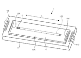
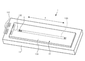
- FIG. 2 is a plan view of the flexible substrate 16 on which the pressure pulse wave sensor 1 shown in FIG. 1 is mounted.
- the flexible substrate 16 has a rectangular shape whose longitudinal direction is a direction Y orthogonal to the direction X, which is one direction, and two pressure pulse wave sensors 1 and a connector 16C are mounted on the surface thereof. .
- the flexible substrate 16 is provided with wiring connected to the connection terminals of the two pressure pulse wave sensors 1 in a resin film. Each wiring is routed to the connector 16C.
- the connector 16C and a connector of a circuit board (not shown) on which the control unit 3 and the like in FIG. 1 are formed are connected.
- the flexible substrate 16 has through holes 16A and 16B substantially in the center of the region where each of the two pressure pulse wave sensors 1 is mounted.
- the through holes 16A and 16B will be described later.
- FIG. 3 is a schematic sectional view taken along line AA shown in FIG.
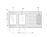
- FIG. 4 is a perspective view showing a main configuration of the pressure pulse wave sensor 1 viewed from the side in contact with the skin. In FIG. 4, illustration of some components is omitted. In FIG. 3, components other than the flexible substrate 16 constitute the pressure pulse wave sensor 1.
- the pressure pulse wave sensor 1 includes a sensor chip 10 and a flat substrate 11.
- the sensor chip 10 includes a semiconductor substrate 10A such as a silicon single crystal or a single crystal of a compound semiconductor such as gallium-arsenide.
- the semiconductor substrate 10A has a rectangular shape in which the direction X is the longitudinal direction.
- the substrate 11 is composed of a hard substrate having sufficiently higher rigidity than the semiconductor substrate 10A such as a ceramic substrate or a glass substrate.
- the substrate 11 has a rectangular shape in which the direction X is the longitudinal direction.
- the surface of the semiconductor substrate 10 ⁇ / b> A (the surface that comes into contact with the skin of a living body) is composed of a bridge having four strain resistance elements, and a plurality of pressure sensitive elements S for detecting contact pressure. Are arranged along the direction X.
- the plurality of pressure sensitive elements S arranged in the direction X constitute a pressure sensitive element row 10D.
- illustration of the pressure sensitive element S is abbreviate
- the surface opposite to the surface on which the pressure-sensitive element array 10 ⁇ / b> D is formed (hereinafter referred to as pressure-sensitive surface) is perpendicular to the pressure-sensitive surface (hereinafter referred to as sensor pressing direction).
- a recess 10a that is recessed is formed.
- the semiconductor substrate 10A is configured to have a thin portion (diaphragm) whose thickness in the sensor pressing direction is thinner than other portions due to the recess 10a.
- column 10D is formed in the area
- the portion excluding the recess 10a (in other words, the surface where the recess 10a is formed) is fixed to the surface of the substrate 11 by the adhesive 12.
- the adhesive 12 for example, a resin material such as an ultraviolet curable resin is used.
- the semiconductor substrate 10A is fixed to the surface of the substrate 11 so that the recess 10a of the semiconductor substrate 10A communicates with the atmosphere only through the through hole 11D formed in the substrate 11.
- One pressure pulse wave sensor 1 of the two pressure pulse wave sensors 1 of the blood pressure measurement device 100 is mounted on the flexible substrate 16 so that the through hole 11D and the through hole 16A overlap in a plan view viewed from the pressure-sensitive surface side. Is done.
- the other of the two pressure pulse wave sensors 1 of the blood pressure measurement device 100 is mounted on the flexible substrate 16 so that the through hole 11D and the through hole 16B overlap in the same plan view. .
- the space defined by the semiconductor substrate 10 ⁇ / b> A, the adhesive 12, and the substrate 11 is divided into the through hole 11 ⁇ / b> D of the substrate 11 and the through hole 16 ⁇ / b> A (or the through hole 16 ⁇ / b> B) of the flexible substrate 16. Is maintained at atmospheric pressure (reference pressure).
- the first terminal portion 10B and the second terminal portion 10C that are electrically connected to the pressure-sensitive element array 10D are disposed at both ends in the direction X of the pressure-sensitive surface of the semiconductor substrate 10A.
- the first terminal portion 10B and the second terminal portion 10C are each composed of a plurality of electrode pads arranged in a direction Y orthogonal to the direction X.
- the surface of the substrate 11 to which the semiconductor substrate 10A is bonded and fixed is electrically connected to the third terminal portion 11B and the second terminal portion 10C for electrical connection to the first terminal portion 10B.
- the fourth terminal portion 11C is provided.
- the third terminal portion 11B, the first terminal portion 10B, the second terminal portion 10C, and the fourth terminal portion 11C are oriented in this order in a plan view as viewed from the direction perpendicular to the pressure-sensitive surface of the semiconductor substrate 10A.
- X is arranged side by side.
- the third terminal portion 11B and the fourth terminal portion 11C are each composed of a plurality of electrode pads arranged in a direction Y orthogonal to the direction X. Each terminal of the third terminal portion 11B corresponds to one of the terminals of the first terminal portion 10B. Each terminal of the fourth terminal portion 11C corresponds to one of the terminals of the second terminal portion 10C.
- each terminal of the first terminal portion 10B and the corresponding terminal of the third terminal portion 11B are electrically connected by a wire W1 that is a first conductive member.
- Each terminal of the second terminal portion 10C and the corresponding terminal of the fourth terminal portion 11C are electrically connected by a wire W2 that is a second conductive member.
- the substrate 11 includes a connection terminal connected to each terminal of the third terminal portion 11B and a connection terminal connected to each terminal of the fourth terminal portion 11C on the flexible substrate 16 side. It is exposed on the surface. These connection terminals are connected to the wiring terminals of the flexible substrate 16.
- the wire W1 and the wire W2 are individually covered and protected by the protective member 13.
- the protective member 13 for example, an epoxy resin or a silicone resin is used.
- the resin material for protecting the wire a material whose volume changes greatly due to environmental conditions such as temperature and humidity is often used.
- the pressure-sensitive surface of the semiconductor substrate 10A, the protective member 13 of the wire W1, and the protective member 13 of the wire W2 are covered with a surface coating layer 15 for protecting the surface of the pressure pulse wave sensor 1.
- the surface coating layer 15 is made of, for example, a silicone resin.
- the pressure pulse wave sensor 1 configured as described above has the pressure-sensitive element array 10D in a state where the pressure-sensitive element array 10D is located immediately above the artery and the direction X intersects (preferably orthogonally) the running direction of the artery.
- the pressure-sensitive surface of the semiconductor substrate 10A on which 10D is formed is pressed against the body surface of the living body via the surface coating layer 15 and used. Thereby, from each pressure sensitive element S, an electrical signal corresponding to the strain applied to the thin portion of the semiconductor substrate 10A, that is, a signal representing a pressure fluctuation acting on the pressure sensitive element S is output.
- the control unit 3 adjusts the pressing state of the pressure pulse wave sensor 1 on the body surface by the pressing mechanism 2, and based on the signal output from the pressure pulse wave sensor 1, the optimum pressure sensitive element After determining the optimum pressing force, the pressure pulse wave is measured based on the signal output from the optimum pressure-sensitive element at the optimum pressing force, and the biological information such as the blood pressure value and the pulse rate is obtained based on the pressure pulse wave. calculate.
- the protective member 13 is often made of a material whose volume change increases with changes in temperature and humidity.
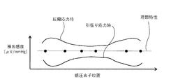
- the pressure pulse wave sensor 1 has a configuration in which the protective member 13 is provided on both ends in the direction X of the pressure-sensitive element array 10D. For this reason, the detection sensitivity of each pressure-sensitive element S in the pressure-sensitive element row 10D is as shown in FIG.
- FIG. 5 shows ideal sensitivity characteristics in which the detection sensitivity of each pressure-sensitive element S is constant, sensitivity characteristics of the pressure-sensitive element array 10D when compressive stress is generated by the protective member 13, and tensile stress by the protective member 13. 4 shows the sensitivity characteristics of the pressure-sensitive element array 10D when the above occurs.
- the pressure-sensitive sensor is located close to the protection member 13 due to the stress generated by the deformation of the protection member 13. It can be seen that the sensitivity varies between the element S and the pressure sensitive element S located far from the protective member 13.
- the sensor chip 10 is fixed to the substrate 11, the sensor chip 10 and the substrate 11 are electrically connected by the conductive members (wires W1, W2), and the conductive member is protected by the protective member 13. In this state, it is important to evaluate the sensor chip 10 based on the signal output from the pressure-sensitive element array 10D.
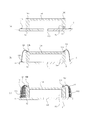
- 6 and 7 are diagrams for explaining an inspection method of the pressure pulse wave sensor 1.
- 6 and 7 correspond to the cross-sectional view of FIG. 3, and the same components as those in FIG. 3 are denoted by the same reference numerals.
- a sensor chip 10 in which a first terminal portion 10B, a second terminal portion 10C, and a pressure sensitive element array 10D are formed on a semiconductor substrate 10A, a third terminal portion 11B, and a fourth terminal portion 11C are provided.
- a formed substrate 11 is prepared.
- the sensor chip 10 is fixed to the surface of the substrate 11 with the adhesive 12 in a state where the recess 10a is superimposed on the region including the through hole 11D of the substrate 11.
- each terminal of the first terminal portion 10B and a terminal of the third terminal portion 11B corresponding to each terminal are connected by the wire W1.
- each terminal of the second terminal portion 10C and a terminal of the fourth terminal portion 11C corresponding to each terminal are connected by a wire W2.
- the element is mounted on the flexible substrate 16 in a state where the through hole 11D of the element in the process of creating the state of FIG. 6C and the through hole 16A of the flexible substrate 16 are overlapped. Thereby, the connector 16C of the flexible substrate 16 and the pressure-sensitive element array 10D are electrically connected.
- the connector 16C is connected to an inspection device that acquires the output signal of each pressure-sensitive element S of the pressure-sensitive element array 10D and performs a process of evaluating the characteristics of the sensor chip 10 based on the acquired output signal.
- the flexible substrate 16 is set in the suction device 30 so that the suction hole 30a of the suction device 30 having the suction hole 30a for sucking air and the through hole 16A overlap.
- the suction device 30 sucks air from the suction hole 30a, the pressure in the space defined by the semiconductor substrate 10A, the adhesive material 12, and the substrate 11 is reduced, and the pressure of the semiconductor substrate 10A in which the pressure-sensitive element array 10D is formed is reduced. Negative pressure is applied to the thin portion.
- the output signal of each pressure-sensitive element S is acquired by the above-described inspection apparatus, and the characteristic evaluation of the sensor chip 10 is performed according to a predetermined evaluation algorithm. This characteristic evaluation is performed while changing the temperature and humidity of the environment where the pressure pulse wave sensor 1 in the process of creation is placed.
- a variation in the detection sensitivity of each pressure-sensitive element S in the pressure-sensitive element row 10D is obtained, and an element in which the variation is within an allowable range is determined to be acceptable.
- the element in the process of being determined to pass is transferred to the surface coating process.
- the two protective members 13 and the exposed surface of the sensor chip 10 are covered with a protective material such as a silicone-based resin to form the surface coating layer 15.
- the surface coating layer 15 covers and protects the sensor chip 10 and the protective member 13 and constitutes a protective layer.
- the characteristic evaluation of the sensor chip 10 is performed in the state where the protective member 13 having a high possibility of affecting the characteristic of the pressure-sensitive element array 10D is formed, the pressure pulse wave due to the change of the use environment Thus, it becomes possible to manufacture a pressure pulse wave sensor with improved pressure pulse wave detection accuracy.
- the characteristic evaluation of the sensor chip 10 can be performed without touching the semiconductor substrate 10A. For this reason, it is possible to evaluate the characteristics before forming the surface coating layer 15 and to improve the production efficiency because it is not necessary to form the surface coating layer 15 for the rejected elements. Can do.
- the characteristic evaluation of the sensor chip 10 is performed after the protective member 13 is formed.
- the characteristics of the sensor chip 10 may be evaluated by mounting the substrate 11 on the flexible substrate 16 from the state of FIG. 6B and performing air suction from the through hole 11D and the through hole 16A.
- the characteristics of the sensor chip 10 may change due to variations in the amount of the adhesive 12 applied.
- the adhesive 12 when a material that changes in volume depending on temperature and humidity is used as the adhesive 12, it can be considered that the characteristics of the sensor chip 10 change depending on the use environment.
- the rejected element can be identified at an early stage, and the production efficiency can be improved.
- the protective member 13 is formed after the characteristic evaluation of the sensor chip 10. For example, if a protective member 13 having a small volume change due to temperature and humidity is used, the sensor chip 10 is subjected to the characteristic evaluation after the characteristic evaluation. The characteristic can be prevented from changing greatly, and the performance can be ensured. Further, in this modification, after the protective member 13 is formed, the surface coating layer 15 is formed by covering the exposed surface of the sensor chip 10 and the protective member 13 with a protective material such as a resin, thereby forming the pressure pulse wave sensor. Finalize.
- the degree of freedom in selecting the material of the protection member 13 is increased, and the inspection is performed in consideration of the influence of both the adhesive 12 and the protection member 13 on the characteristics of the pressure-sensitive element array 10D. Therefore, it can be particularly preferably implemented.
- the pressure pulse wave sensor 1 is provided with chip-side terminal portions composed of a first terminal portion 10B and a second terminal portion 10C at both ends in the direction X of the pressure-sensitive surface of the semiconductor substrate 10A, and the first terminal portion 10B. And the board side terminal part comprised by the 3rd terminal part 11B and the 4th terminal part 11C corresponding to each of the 2nd terminal part 10C was set.
- a chip-side terminal portion including terminals electrically connected to each pressure-sensitive element S only at one of both end portions in the direction X of the pressure-sensitive surface of the semiconductor substrate 10A. 10E may be provided.
- a substrate-side terminal portion 11E made of may be formed.
- the pressure-sensitive element S located at a position close to the protective member due to the stress generated by the deformation of the protective member that covers the conductive member that connects the chip-side terminal portion 10E and the substrate-side terminal portion 11E.
- the sensitivity may vary with the pressure sensitive element S located far from the protective member. For this reason, the inspection method of this embodiment which can test
- the pressure pulse wave sensor 1 is advantageous for downsizing.
- a wrist-mounted blood pressure measuring device that detects a pressure pulse wave of the radial artery of the wrist has been described, but it may be applied to the carotid artery or the dorsal artery.
- the pressure-sensitive element S for detecting the contact pressure is not limited to the one using the bridge circuit and the diaphragm, but may be another known configuration.
- the blood pressure measurement device 100 has two pressure pulse wave sensors 1. However, if there is at least one pressure pulse wave sensor 1, it is possible to detect the pressure pulse wave and measure biological information. is there.
- connection between each terminal of the first terminal portion 10B and the corresponding terminal of the third terminal portion 11B is not limited to a wire, and may be performed by a conductive member such as a conductive paste.
- connection between each terminal of the second terminal portion 10C and the corresponding terminal of the fourth terminal portion 11C is not limited to a wire, and may be performed by a conductive member such as a conductive paste, for example.
- the protective member 13 for protecting the wiring formed by the conductive member is necessary, and the present invention is effective.
- the connector 16C of the flexible substrate 16 and the inspection device are connected and the characteristics of the sensor chip 10 are evaluated.
- An inspection probe may be brought into contact with the connection terminal exposed to the signal to take out a signal from the sensor chip 10. In this case, the flexible board is not wasted in the rejected element.
- the disclosed method for inspecting a pressure pulse wave sensor includes: a pressure-sensitive element array including a plurality of pressure-sensitive elements arranged in one direction; and a chip-side terminal portion electrically connected to the pressure-sensitive element array.
- a sensor chip that is used by pressing a pressure-sensitive surface on which the pressure-sensitive element array is formed against the body surface of the living body in a state where the one direction intersects the running direction of the artery of the living body, and the sensor
- a pressure pulse wave sensor inspection method comprising a substrate to which a chip is fixed and having a through-hole, wherein the sensor chip has a recess recessed in a direction perpendicular to the pressure-sensitive surface.
- the sensor chip A second step of connecting the substrate-side terminal portion of the fixed substrate and the chip-side terminal portion by a conductive member; and after the second step, air is sucked from the through-hole of the substrate to achieve the feeling.
- the chip-side terminal portion includes a first terminal portion and a second terminal portion respectively disposed at both ends of the pressure-sensitive surface in the one direction, and the substrate
- the side terminal portion includes a third terminal portion and a fourth terminal portion formed on a surface to which the sensor chip of the substrate is bonded and fixed, and when viewed from a direction perpendicular to the pressure sensitive surface, Three terminal portions, the first terminal portion, the second terminal portion, and the fourth terminal portion are arranged in the one direction in this order, and in the second step, the first terminal And the third terminal portion are connected by a first conductive member, the second terminal portion and the fourth terminal portion are connected by a second conductive member, and prior to the third step. , Holding the first conductive member and the second conductive member formed in the second step, respectively.
- a fourth step of covering a member is further comprising.
- the disclosed method for manufacturing a pressure pulse wave sensor includes: a pressure-sensitive element array including a plurality of pressure-sensitive elements arranged in one direction; and a chip-side terminal portion electrically connected to the pressure-sensitive element array.
- a sensor chip that is used by pressing a pressure-sensitive surface on which the pressure-sensitive element array is formed against the body surface of the living body in a state where the one direction intersects the running direction of the artery of the living body, and the sensor
- a pressure pulse wave sensor having a substrate to which a chip is fixed and having a through-hole, wherein the sensor chip has a concave portion recessed in a direction perpendicular to the pressure-sensitive surface, and the concave portion is provided in the direction.
- the sensor chip A second step of connecting the substrate-side terminal portion of the fixed substrate and the chip-side terminal portion by a conductive member; and after the second step, air is sucked from the through-hole of the substrate to achieve the feeling.
- a third step of performing the characteristic evaluation of the sensor chip based on a signal output from the substrate side terminal portion, and a result of the characteristic evaluation of the third step And a fifth step of forming a protective layer that protects the sensor chip determined to be acceptable and the conductive member connecting the chip side terminal portion and the substrate side terminal portion of the sensor chip.
- the chip-side terminal portion includes a first terminal portion and a second terminal portion respectively disposed at both ends of the pressure-sensitive surface in the one direction, and the substrate
- the side terminal portion includes a third terminal portion and a fourth terminal portion formed on a surface to which the sensor chip of the substrate is bonded and fixed, and when viewed from a direction perpendicular to the pressure sensitive surface, Three terminal portions, the first terminal portion, the second terminal portion, and the fourth terminal portion are arranged in the one direction in this order, and in the second step, the first terminal And the third terminal portion are connected by a first conductive member, the second terminal portion and the fourth terminal portion are connected by a second conductive member, and prior to the third step.
- the fifth step is to form the protective layer by covering the protective member and the exposed surface of the sensor chip with a protective material.
- the present invention it is possible to provide an inspection method and a manufacturing method of a pressure pulse wave sensor capable of knowing the influence on the detection accuracy of the pressure pulse wave due to a change in use environment.
Landscapes
- Health & Medical Sciences (AREA)
- Life Sciences & Earth Sciences (AREA)
- Physics & Mathematics (AREA)
- Engineering & Computer Science (AREA)
- Cardiology (AREA)
- Medical Informatics (AREA)
- General Health & Medical Sciences (AREA)
- Biophysics (AREA)
- Pathology (AREA)
- Veterinary Medicine (AREA)
- Biomedical Technology (AREA)
- Heart & Thoracic Surgery (AREA)
- Public Health (AREA)
- Molecular Biology (AREA)
- Surgery (AREA)
- Animal Behavior & Ethology (AREA)
- General Physics & Mathematics (AREA)
- Physiology (AREA)
- Vascular Medicine (AREA)
- Chemical & Material Sciences (AREA)
- Analytical Chemistry (AREA)
- Ophthalmology & Optometry (AREA)
- Signal Processing (AREA)
- Child & Adolescent Psychology (AREA)
- Optics & Photonics (AREA)
- Measuring Pulse, Heart Rate, Blood Pressure Or Blood Flow (AREA)
Priority Applications (3)
| Application Number | Priority Date | Filing Date | Title |
|---|---|---|---|
| EP16844245.7A EP3332702B1 (en) | 2015-09-07 | 2016-08-31 | Method of inspecting pressure pulse wave sensor, and method of manufacturing pressure pulse wave sensor |
| CN201680051684.5A CN108024736B (zh) | 2015-09-07 | 2016-08-31 | 压力脉搏波传感器的检查方法及压力脉搏波传感器的制造方法 |
| US15/914,711 US10136858B2 (en) | 2015-09-07 | 2018-03-07 | Method for inspecting pressure pulse wave sensor and method for manufacturing pressure pulse wave sensor |
Applications Claiming Priority (2)
| Application Number | Priority Date | Filing Date | Title |
|---|---|---|---|
| JP2015175967A JP6540397B2 (ja) | 2015-09-07 | 2015-09-07 | 圧脈波センサの検査方法及び圧脈波センサの製造方法 |
| JP2015-175967 | 2015-09-07 |
Related Child Applications (1)
| Application Number | Title | Priority Date | Filing Date |
|---|---|---|---|
| US15/914,711 Continuation US10136858B2 (en) | 2015-09-07 | 2018-03-07 | Method for inspecting pressure pulse wave sensor and method for manufacturing pressure pulse wave sensor |
Publications (1)
| Publication Number | Publication Date |
|---|---|
| WO2017043384A1 true WO2017043384A1 (ja) | 2017-03-16 |
Family
ID=58239753
Family Applications (1)
| Application Number | Title | Priority Date | Filing Date |
|---|---|---|---|
| PCT/JP2016/075435 WO2017043384A1 (ja) | 2015-09-07 | 2016-08-31 | 圧脈波センサの検査方法及び圧脈波センサの製造方法 |
Country Status (5)
| Country | Link |
|---|---|
| US (1) | US10136858B2 (zh) |
| EP (1) | EP3332702B1 (zh) |
| JP (1) | JP6540397B2 (zh) |
| CN (1) | CN108024736B (zh) |
| WO (1) | WO2017043384A1 (zh) |
Families Citing this family (3)
| Publication number | Priority date | Publication date | Assignee | Title |
|---|---|---|---|---|
| CN111565637A (zh) | 2017-10-09 | 2020-08-21 | 钛深科技 | 基于可穿戴压力传感器阵列的人体动作和位置感测、识别与分析 |
| CN110255491A (zh) * | 2019-06-27 | 2019-09-20 | 中国科学院微电子研究所 | Mems压力传感器封装结构及封装方法 |
| CN110763393A (zh) * | 2019-09-21 | 2020-02-07 | 蚌埠市力业传感器有限公司 | 压力传感器 |
Citations (5)
| Publication number | Priority date | Publication date | Assignee | Title |
|---|---|---|---|---|
| JPS63118629A (ja) * | 1986-11-06 | 1988-05-23 | Sumitomo Electric Ind Ltd | 半導体圧力センサのブリツジ回路調整方法 |
| JPH0225050A (ja) * | 1988-07-13 | 1990-01-26 | Fujikura Ltd | 半導体圧力のセンサの特性測定方法 |
| JPH0467839A (ja) * | 1990-07-06 | 1992-03-03 | Colleen Denshi Kk | 接触圧センサ |
| JP2009517137A (ja) * | 2005-11-23 | 2009-04-30 | バイタル センサーズ,インコーポレイテッド | 心臓内の血圧/温度の遠隔計測用植込み型装置 |
| JP2015144628A (ja) * | 2014-01-31 | 2015-08-13 | オムロンヘルスケア株式会社 | 脈波検出装置 |
Family Cites Families (10)
| Publication number | Priority date | Publication date | Assignee | Title |
|---|---|---|---|---|
| JPS56107142A (en) * | 1980-01-31 | 1981-08-25 | Toshiba Corp | Property evaluation device for semiconductor pressure detection element |
| US4809536A (en) * | 1986-11-06 | 1989-03-07 | Sumitomo Electric Industries, Ltd. | Method of adjusting bridge circuit of semiconductor pressure sensor |
| JP2798764B2 (ja) * | 1990-01-09 | 1998-09-17 | コーリン電子株式会社 | 半導体圧脈波センサ |
| JP2894798B2 (ja) * | 1990-06-27 | 1999-05-24 | 日本硝子繊維株式会社 | ゴム補強用ガラス繊維の処理剤 |
| US5179956A (en) | 1990-07-06 | 1993-01-19 | Colin Electronics Co., Ltd. | Contact pressure sensor |
| US6159166A (en) * | 1998-03-20 | 2000-12-12 | Hypertension Diagnostics, Inc. | Sensor and method for sensing arterial pulse pressure |
| FR2817756B1 (fr) * | 2000-12-08 | 2008-10-31 | Hospal Internat Marketing Man | Dispositif pour la mesure de pression comportant un capteur d'effort motorise |
| JP4363157B2 (ja) | 2002-11-29 | 2009-11-11 | オムロンヘルスケア株式会社 | 脈波測定装置 |
| CN2631047Y (zh) * | 2003-03-14 | 2004-08-04 | 徐杏芬 | 发光二极管的热传导及光度提升结构的改进 |
| US7686768B2 (en) | 2005-11-23 | 2010-03-30 | Vital Sensors Holding Company, Inc. | Implantable pressure monitor |
-
2015
- 2015-09-07 JP JP2015175967A patent/JP6540397B2/ja active Active
-
2016
- 2016-08-31 WO PCT/JP2016/075435 patent/WO2017043384A1/ja active Application Filing
- 2016-08-31 EP EP16844245.7A patent/EP3332702B1/en active Active
- 2016-08-31 CN CN201680051684.5A patent/CN108024736B/zh active Active
-
2018
- 2018-03-07 US US15/914,711 patent/US10136858B2/en active Active
Patent Citations (5)
| Publication number | Priority date | Publication date | Assignee | Title |
|---|---|---|---|---|
| JPS63118629A (ja) * | 1986-11-06 | 1988-05-23 | Sumitomo Electric Ind Ltd | 半導体圧力センサのブリツジ回路調整方法 |
| JPH0225050A (ja) * | 1988-07-13 | 1990-01-26 | Fujikura Ltd | 半導体圧力のセンサの特性測定方法 |
| JPH0467839A (ja) * | 1990-07-06 | 1992-03-03 | Colleen Denshi Kk | 接触圧センサ |
| JP2009517137A (ja) * | 2005-11-23 | 2009-04-30 | バイタル センサーズ,インコーポレイテッド | 心臓内の血圧/温度の遠隔計測用植込み型装置 |
| JP2015144628A (ja) * | 2014-01-31 | 2015-08-13 | オムロンヘルスケア株式会社 | 脈波検出装置 |
Non-Patent Citations (1)
| Title |
|---|
| See also references of EP3332702A4 * |
Also Published As
| Publication number | Publication date |
|---|---|
| US10136858B2 (en) | 2018-11-27 |
| EP3332702A4 (en) | 2019-04-17 |
| EP3332702B1 (en) | 2020-05-27 |
| CN108024736B (zh) | 2020-09-25 |
| US20180192956A1 (en) | 2018-07-12 |
| JP2017051277A (ja) | 2017-03-16 |
| CN108024736A (zh) | 2018-05-11 |
| JP6540397B2 (ja) | 2019-07-10 |
| EP3332702A1 (en) | 2018-06-13 |
Similar Documents
| Publication | Publication Date | Title |
|---|---|---|
| US9581427B2 (en) | Mechanical quantity measuring device | |
| CN107445133B (zh) | 对热机械封装应力具有低灵敏度的小型负荷传感器装置 | |
| US10136858B2 (en) | Method for inspecting pressure pulse wave sensor and method for manufacturing pressure pulse wave sensor | |
| JP2014048072A (ja) | 圧力センサモジュール | |
| US11344207B2 (en) | Pressure pulse wave sensor and biological information measurement device | |
| KR101573367B1 (ko) | 압저항형 세라믹 압력센서 | |
| JP2017051277A5 (zh) | ||
| CN107490337B (zh) | 应变检测器及其制造方法 | |
| EP3660476B1 (en) | Cost overmolded leadframe force sensor with multiple mounting positions | |
| JP5804445B2 (ja) | 半導体圧力センサ | |
| US20180266909A1 (en) | Component having a micromechanical sensor module | |
| JP2009288170A (ja) | 半導体圧力センサ | |
| JP2008082952A (ja) | 半導体感歪センサ | |
| JP6524858B2 (ja) | 脈波測定装置 | |
| JP4706634B2 (ja) | 半導体センサおよびその製造方法 | |
| US20150082898A1 (en) | Strain sensor | |
| JP7474964B2 (ja) | デバイス製造装置の検査方法及びデバイス製造装置 | |
| JP2010071817A (ja) | 半導体センサ内蔵パッケージ | |
| KR20110059028A (ko) | 반도체 스트레인게이지형 압력센서모듈과 그 제조방법 | |
| JP2000046669A (ja) | 圧力センサ |
Legal Events
| Date | Code | Title | Description |
|---|---|---|---|
| 121 | Ep: the epo has been informed by wipo that ep was designated in this application |
Ref document number: 16844245 Country of ref document: EP Kind code of ref document: A1 |
|
| NENP | Non-entry into the national phase |
Ref country code: DE |
|
| WWE | Wipo information: entry into national phase |
Ref document number: 2016844245 Country of ref document: EP |