WO2017042941A1 - 表示装置及び表示装置の製造方法 - Google Patents
表示装置及び表示装置の製造方法 Download PDFInfo
- Publication number
- WO2017042941A1 WO2017042941A1 PCT/JP2015/075759 JP2015075759W WO2017042941A1 WO 2017042941 A1 WO2017042941 A1 WO 2017042941A1 JP 2015075759 W JP2015075759 W JP 2015075759W WO 2017042941 A1 WO2017042941 A1 WO 2017042941A1
- Authority
- WO
- WIPO (PCT)
- Prior art keywords
- thin film
- film transistor
- region
- channel region
- polysilicon
- Prior art date
- Legal status (The legal status is an assumption and is not a legal conclusion. Google has not performed a legal analysis and makes no representation as to the accuracy of the status listed.)
- Ceased
Links
Images







Classifications
-
- G—PHYSICS
- G02—OPTICS
- G02F—OPTICAL DEVICES OR ARRANGEMENTS FOR THE CONTROL OF LIGHT BY MODIFICATION OF THE OPTICAL PROPERTIES OF THE MEDIA OF THE ELEMENTS INVOLVED THEREIN; NON-LINEAR OPTICS; FREQUENCY-CHANGING OF LIGHT; OPTICAL LOGIC ELEMENTS; OPTICAL ANALOGUE/DIGITAL CONVERTERS
- G02F1/00—Devices or arrangements for the control of the intensity, colour, phase, polarisation or direction of light arriving from an independent light source, e.g. switching, gating or modulating; Non-linear optics
- G02F1/01—Devices or arrangements for the control of the intensity, colour, phase, polarisation or direction of light arriving from an independent light source, e.g. switching, gating or modulating; Non-linear optics for the control of the intensity, phase, polarisation or colour
- G02F1/13—Devices or arrangements for the control of the intensity, colour, phase, polarisation or direction of light arriving from an independent light source, e.g. switching, gating or modulating; Non-linear optics for the control of the intensity, phase, polarisation or colour based on liquid crystals, e.g. single liquid crystal display cells
- G02F1/133—Constructional arrangements; Operation of liquid crystal cells; Circuit arrangements
- G02F1/136—Liquid crystal cells structurally associated with a semi-conducting layer or substrate, e.g. cells forming part of an integrated circuit
- G02F1/1362—Active matrix addressed cells
- G02F1/1368—Active matrix addressed cells in which the switching element is a three-electrode device
-
- G—PHYSICS
- G02—OPTICS
- G02F—OPTICAL DEVICES OR ARRANGEMENTS FOR THE CONTROL OF LIGHT BY MODIFICATION OF THE OPTICAL PROPERTIES OF THE MEDIA OF THE ELEMENTS INVOLVED THEREIN; NON-LINEAR OPTICS; FREQUENCY-CHANGING OF LIGHT; OPTICAL LOGIC ELEMENTS; OPTICAL ANALOGUE/DIGITAL CONVERTERS
- G02F1/00—Devices or arrangements for the control of the intensity, colour, phase, polarisation or direction of light arriving from an independent light source, e.g. switching, gating or modulating; Non-linear optics
- G02F1/01—Devices or arrangements for the control of the intensity, colour, phase, polarisation or direction of light arriving from an independent light source, e.g. switching, gating or modulating; Non-linear optics for the control of the intensity, phase, polarisation or colour
- G02F1/13—Devices or arrangements for the control of the intensity, colour, phase, polarisation or direction of light arriving from an independent light source, e.g. switching, gating or modulating; Non-linear optics for the control of the intensity, phase, polarisation or colour based on liquid crystals, e.g. single liquid crystal display cells
- G02F1/133—Constructional arrangements; Operation of liquid crystal cells; Circuit arrangements
- G02F1/1333—Constructional arrangements; Manufacturing methods
- G02F1/1345—Conductors connecting electrodes to cell terminals
- G02F1/13454—Drivers integrated on the active matrix substrate
-
- G—PHYSICS
- G02—OPTICS
- G02F—OPTICAL DEVICES OR ARRANGEMENTS FOR THE CONTROL OF LIGHT BY MODIFICATION OF THE OPTICAL PROPERTIES OF THE MEDIA OF THE ELEMENTS INVOLVED THEREIN; NON-LINEAR OPTICS; FREQUENCY-CHANGING OF LIGHT; OPTICAL LOGIC ELEMENTS; OPTICAL ANALOGUE/DIGITAL CONVERTERS
- G02F1/00—Devices or arrangements for the control of the intensity, colour, phase, polarisation or direction of light arriving from an independent light source, e.g. switching, gating or modulating; Non-linear optics
- G02F1/01—Devices or arrangements for the control of the intensity, colour, phase, polarisation or direction of light arriving from an independent light source, e.g. switching, gating or modulating; Non-linear optics for the control of the intensity, phase, polarisation or colour
- G02F1/13—Devices or arrangements for the control of the intensity, colour, phase, polarisation or direction of light arriving from an independent light source, e.g. switching, gating or modulating; Non-linear optics for the control of the intensity, phase, polarisation or colour based on liquid crystals, e.g. single liquid crystal display cells
- G02F1/133—Constructional arrangements; Operation of liquid crystal cells; Circuit arrangements
- G02F1/136—Liquid crystal cells structurally associated with a semi-conducting layer or substrate, e.g. cells forming part of an integrated circuit
- G02F1/1362—Active matrix addressed cells
- G02F1/136227—Through-hole connection of the pixel electrode to the active element through an insulation layer
-
- G—PHYSICS
- G02—OPTICS
- G02F—OPTICAL DEVICES OR ARRANGEMENTS FOR THE CONTROL OF LIGHT BY MODIFICATION OF THE OPTICAL PROPERTIES OF THE MEDIA OF THE ELEMENTS INVOLVED THEREIN; NON-LINEAR OPTICS; FREQUENCY-CHANGING OF LIGHT; OPTICAL LOGIC ELEMENTS; OPTICAL ANALOGUE/DIGITAL CONVERTERS
- G02F1/00—Devices or arrangements for the control of the intensity, colour, phase, polarisation or direction of light arriving from an independent light source, e.g. switching, gating or modulating; Non-linear optics
- G02F1/01—Devices or arrangements for the control of the intensity, colour, phase, polarisation or direction of light arriving from an independent light source, e.g. switching, gating or modulating; Non-linear optics for the control of the intensity, phase, polarisation or colour
- G02F1/13—Devices or arrangements for the control of the intensity, colour, phase, polarisation or direction of light arriving from an independent light source, e.g. switching, gating or modulating; Non-linear optics for the control of the intensity, phase, polarisation or colour based on liquid crystals, e.g. single liquid crystal display cells
- G02F1/133—Constructional arrangements; Operation of liquid crystal cells; Circuit arrangements
- G02F1/136—Liquid crystal cells structurally associated with a semi-conducting layer or substrate, e.g. cells forming part of an integrated circuit
- G02F1/1362—Active matrix addressed cells
- G02F1/136286—Wiring, e.g. gate line, drain line
-
- H—ELECTRICITY
- H10—SEMICONDUCTOR DEVICES; ELECTRIC SOLID-STATE DEVICES NOT OTHERWISE PROVIDED FOR
- H10D—INORGANIC ELECTRIC SEMICONDUCTOR DEVICES
- H10D30/00—Field-effect transistors [FET]
- H10D30/60—Insulated-gate field-effect transistors [IGFET]
- H10D30/67—Thin-film transistors [TFT]
- H10D30/6729—Thin-film transistors [TFT] characterised by the electrodes
- H10D30/6737—Thin-film transistors [TFT] characterised by the electrodes characterised by the electrode materials
- H10D30/6739—Conductor-insulator-semiconductor electrodes
-
- H—ELECTRICITY
- H10—SEMICONDUCTOR DEVICES; ELECTRIC SOLID-STATE DEVICES NOT OTHERWISE PROVIDED FOR
- H10D—INORGANIC ELECTRIC SEMICONDUCTOR DEVICES
- H10D30/00—Field-effect transistors [FET]
- H10D30/60—Insulated-gate field-effect transistors [IGFET]
- H10D30/67—Thin-film transistors [TFT]
- H10D30/674—Thin-film transistors [TFT] characterised by the active materials
-
- H—ELECTRICITY
- H10—SEMICONDUCTOR DEVICES; ELECTRIC SOLID-STATE DEVICES NOT OTHERWISE PROVIDED FOR
- H10D—INORGANIC ELECTRIC SEMICONDUCTOR DEVICES
- H10D30/00—Field-effect transistors [FET]
- H10D30/60—Insulated-gate field-effect transistors [IGFET]
- H10D30/67—Thin-film transistors [TFT]
- H10D30/674—Thin-film transistors [TFT] characterised by the active materials
- H10D30/6741—Group IV materials, e.g. germanium or silicon carbide
- H10D30/6743—Silicon
- H10D30/6745—Polycrystalline or microcrystalline silicon
-
- H—ELECTRICITY
- H10—SEMICONDUCTOR DEVICES; ELECTRIC SOLID-STATE DEVICES NOT OTHERWISE PROVIDED FOR
- H10D—INORGANIC ELECTRIC SEMICONDUCTOR DEVICES
- H10D30/00—Field-effect transistors [FET]
- H10D30/60—Insulated-gate field-effect transistors [IGFET]
- H10D30/67—Thin-film transistors [TFT]
- H10D30/6757—Thin-film transistors [TFT] characterised by the structure of the channel, e.g. transverse or longitudinal shape or doping profile
-
- H—ELECTRICITY
- H10—SEMICONDUCTOR DEVICES; ELECTRIC SOLID-STATE DEVICES NOT OTHERWISE PROVIDED FOR
- H10D—INORGANIC ELECTRIC SEMICONDUCTOR DEVICES
- H10D86/00—Integrated devices formed in or on insulating or conducting substrates, e.g. formed in silicon-on-insulator [SOI] substrates or on stainless steel or glass substrates
- H10D86/01—Manufacture or treatment
- H10D86/021—Manufacture or treatment of multiple TFTs
- H10D86/0231—Manufacture or treatment of multiple TFTs using masks, e.g. half-tone masks
-
- H—ELECTRICITY
- H10—SEMICONDUCTOR DEVICES; ELECTRIC SOLID-STATE DEVICES NOT OTHERWISE PROVIDED FOR
- H10D—INORGANIC ELECTRIC SEMICONDUCTOR DEVICES
- H10D86/00—Integrated devices formed in or on insulating or conducting substrates, e.g. formed in silicon-on-insulator [SOI] substrates or on stainless steel or glass substrates
- H10D86/40—Integrated devices formed in or on insulating or conducting substrates, e.g. formed in silicon-on-insulator [SOI] substrates or on stainless steel or glass substrates characterised by multiple TFTs
- H10D86/421—Integrated devices formed in or on insulating or conducting substrates, e.g. formed in silicon-on-insulator [SOI] substrates or on stainless steel or glass substrates characterised by multiple TFTs having a particular composition, shape or crystalline structure of the active layer
-
- H—ELECTRICITY
- H10—SEMICONDUCTOR DEVICES; ELECTRIC SOLID-STATE DEVICES NOT OTHERWISE PROVIDED FOR
- H10D—INORGANIC ELECTRIC SEMICONDUCTOR DEVICES
- H10D86/00—Integrated devices formed in or on insulating or conducting substrates, e.g. formed in silicon-on-insulator [SOI] substrates or on stainless steel or glass substrates
- H10D86/40—Integrated devices formed in or on insulating or conducting substrates, e.g. formed in silicon-on-insulator [SOI] substrates or on stainless steel or glass substrates characterised by multiple TFTs
- H10D86/421—Integrated devices formed in or on insulating or conducting substrates, e.g. formed in silicon-on-insulator [SOI] substrates or on stainless steel or glass substrates characterised by multiple TFTs having a particular composition, shape or crystalline structure of the active layer
- H10D86/425—Integrated devices formed in or on insulating or conducting substrates, e.g. formed in silicon-on-insulator [SOI] substrates or on stainless steel or glass substrates characterised by multiple TFTs having a particular composition, shape or crystalline structure of the active layer having different crystal properties in different TFTs or within an individual TFT
-
- H—ELECTRICITY
- H10—SEMICONDUCTOR DEVICES; ELECTRIC SOLID-STATE DEVICES NOT OTHERWISE PROVIDED FOR
- H10D—INORGANIC ELECTRIC SEMICONDUCTOR DEVICES
- H10D86/00—Integrated devices formed in or on insulating or conducting substrates, e.g. formed in silicon-on-insulator [SOI] substrates or on stainless steel or glass substrates
- H10D86/40—Integrated devices formed in or on insulating or conducting substrates, e.g. formed in silicon-on-insulator [SOI] substrates or on stainless steel or glass substrates characterised by multiple TFTs
- H10D86/441—Interconnections, e.g. scanning lines
-
- H—ELECTRICITY
- H10—SEMICONDUCTOR DEVICES; ELECTRIC SOLID-STATE DEVICES NOT OTHERWISE PROVIDED FOR
- H10D—INORGANIC ELECTRIC SEMICONDUCTOR DEVICES
- H10D86/00—Integrated devices formed in or on insulating or conducting substrates, e.g. formed in silicon-on-insulator [SOI] substrates or on stainless steel or glass substrates
- H10D86/40—Integrated devices formed in or on insulating or conducting substrates, e.g. formed in silicon-on-insulator [SOI] substrates or on stainless steel or glass substrates characterised by multiple TFTs
- H10D86/60—Integrated devices formed in or on insulating or conducting substrates, e.g. formed in silicon-on-insulator [SOI] substrates or on stainless steel or glass substrates characterised by multiple TFTs wherein the TFTs are in active matrices
-
- G—PHYSICS
- G02—OPTICS
- G02F—OPTICAL DEVICES OR ARRANGEMENTS FOR THE CONTROL OF LIGHT BY MODIFICATION OF THE OPTICAL PROPERTIES OF THE MEDIA OF THE ELEMENTS INVOLVED THEREIN; NON-LINEAR OPTICS; FREQUENCY-CHANGING OF LIGHT; OPTICAL LOGIC ELEMENTS; OPTICAL ANALOGUE/DIGITAL CONVERTERS
- G02F2201/00—Constructional arrangements not provided for in groups G02F1/00 - G02F7/00
- G02F2201/12—Constructional arrangements not provided for in groups G02F1/00 - G02F7/00 electrode
- G02F2201/123—Constructional arrangements not provided for in groups G02F1/00 - G02F7/00 electrode pixel
-
- G—PHYSICS
- G02—OPTICS
- G02F—OPTICAL DEVICES OR ARRANGEMENTS FOR THE CONTROL OF LIGHT BY MODIFICATION OF THE OPTICAL PROPERTIES OF THE MEDIA OF THE ELEMENTS INVOLVED THEREIN; NON-LINEAR OPTICS; FREQUENCY-CHANGING OF LIGHT; OPTICAL LOGIC ELEMENTS; OPTICAL ANALOGUE/DIGITAL CONVERTERS
- G02F2202/00—Materials and properties
- G02F2202/10—Materials and properties semiconductor
- G02F2202/103—Materials and properties semiconductor a-Si
Definitions
- the present invention relates to a display device including a picture element having a first thin film transistor and a drive circuit having a second thin film transistor and driving the picture element, and a method of manufacturing the display device.
- TFTs Thin Film Transistor
- a-Si TFT using amorphous silicon (amorphous silicon) for the channel region or a P-Si TFT using polysilicon (poly-crystalline silicon) for the channel region is used.
- the P-Si TFT is manufactured by a laser annealing method in which patterning is performed after irradiating the entire surface of the substrate with laser.
- Patent Document 1 discloses a gate insulating film formed so as to cover a gate electrode, a polysilicon film formed on the gate insulating film, and a source electrode formed above an end of the polysilicon film. And a drain electrode formed above the end of the polysilicon film facing the end where the source electrode is formed and spaced apart from the source electrode, and a source in the polysilicon film Crystals of the polysilicon film from the end of the polysilicon film where the electrode or drain electrode is formed toward the center of the polysilicon film where the source or drain electrode is not formed in the polysilicon film It is disclosed that the conversion rate is reduced.
- a peripheral circuit or a driving circuit for driving a pixel is required to have a high on-current in order to be driven as a circuit.
- the on / off switching is frequently performed in the pixel, it is desirable that the off current is low.
- the P-Si TFT described above has a characteristic that both the current that flows when it is on (on-current) and the current that flows when it is off (off-current) are both high. Therefore, although it is suitable for a TFT for a peripheral circuit or a driving circuit, it is not preferable for a TFT for a pixel.
- the present invention has been made in view of such circumstances, and an object thereof is to include a picture element having a first thin film transistor and a driving circuit having a second thin film transistor and driving the picture element.
- the first channel region related to the first thin film transistor and the second channel region related to the second thin film transistor are configured to have different electrical characteristics (for example, electron mobility).
- An object of the present invention is to provide a display device in which one thin film transistor and a second thin film transistor can operate in accordance with their respective roles, and a method for manufacturing the display device.
- a display device includes a picture element having a first thin film transistor and a drive circuit having a second thin film transistor and driving the picture element, wherein the first thin film transistor has a first channel region.
- the second thin film transistor has a second channel region, the first channel region includes an amorphous silicon region and a polysilicon region, and the first channel region and the second channel region have electrical characteristics. It is characterized by being different.
- the first channel region includes an amorphous silicon region and a polysilicon region
- the second channel region includes only the polysilicon region, whereby the first channel region and the polysilicon region are included.
- the second channel region is configured to have different electrical characteristics.
- a source electrode and a drain electrode are stacked at a predetermined interval on the upper side of a gate electrode with the first channel region interposed therebetween, and the first channel
- the region is characterized in that an amorphous silicon region and a polysilicon region are mixed.
- an amorphous silicon region and a polysilicon region are mixed in the first channel region.
- the polysilicon regions are separated from each other, one polysilicon region overlaps the source electrode in the stacking direction, and the other polysilicon region is In the stacking direction, the drain electrode overlaps with the drain electrode.
- one of the two polysilicon regions overlaps the source electrode in the stacking direction, and the other polysilicon region overlaps in the stacking direction. It overlaps with the drain electrode.
- the two polysilicon regions are formed around the source electrode and the drain electrode, respectively.
- the polysilicon region is long in a direction in which the source electrode and the drain electrode are separated from each other, and both end sides of the polysilicon region are in the stacking direction, and the source electrode and the drain electrode are It is characterized by overlapping with a part of both opposing ends.
- both end sides of the polysilicon region overlap with a part of both opposing ends of the source electrode and the drain electrode in the stacking direction, respectively.
- An adjacent region or a nearby region is an amorphous silicon region.
- the display device is characterized in that the polysilicon region has a dimension in a direction perpendicular to the direction of the separation between the opposite ends of the source electrode and the drain electrode.
- the both ends of the polysilicon region overlap with a part of both opposing ends of the source electrode and the drain electrode in the stacking direction, respectively, and the source electrode and the drain
- the dimension in the direction perpendicular to the direction of the separation increases in the middle between the opposite ends of the electrodes. Therefore, a region adjacent to or near the source electrode and the drain electrode is an amorphous silicon region.
- the polysilicon region is provided at one location, and is interposed between the opposing ends of the source electrode and the drain electrode, and in the stacking direction, the source electrode and the drain electrode It is characterized by not overlapping with both opposite ends of.
- the polysilicon region is located between the opposing ends of the source electrode and the drain electrode so as not to overlap the opposing ends of the source electrode and the drain electrode in the stacking direction.
- a region adjacent to or adjacent to the source electrode and the drain electrode is an amorphous silicon region.
- each of the first thin film transistor and the second thin film transistor has a predetermined interval between the source electrode and the drain electrode above the gate electrode with the first channel region or the second channel region interposed therebetween. Only the polysilicon region exists in the first channel region and the second channel region, and the first channel region and the second channel region have polysilicon crystallinity. Are different.
- the polysilicon region exists in the first channel region and the second channel region, and the first channel region and the second channel region have polysilicon crystallinity. Different.
- a method for manufacturing a display device comprising: a plurality of pixels having first thin film transistors; and a drive circuit having a second thin film transistor and driving the pixels.
- a polysilicon region is selectively formed in the amorphous silicon layer.
- a gate electrode insulating layer for a plurality of gate electrodes is formed, an amorphous silicon layer is formed on the gate electrode insulating layer, and thereafter, a polysilicon region is selected for the amorphous silicon layer.
- a first channel region related to the first thin film transistor is formed.
- an annealing process is performed in which the amorphous silicon layer is partially irradiated with an energy beam to be changed into a polysilicon layer, and the amorphous silicon layer is covered with another amorphous silicon.
- the amorphous silicon layer is partially irradiated with an energy beam to be changed into a polysilicon layer, and then another amorphous silicon layer is formed covering the polysilicon layer.
- An n + silicon layer is formed on the surface of the other amorphous silicon layer.
- the first thin film transistor can surely suppress the off-current, and a drive circuit (peripheral circuit) that needs to increase the on-current.
- the second thin film transistor can surely increase the on-current, so that the first thin film transistor and the second thin film transistor can perform operations suitable for their respective roles.
- FIG. 3 is a functional block diagram illustrating a main configuration of the television receiver according to Embodiment 1.
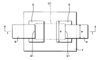
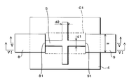
- FIG. 3 is a schematic diagram schematically illustrating an example of a thin film transistor used for a driving circuit and a pixel of the television receiver according to the first embodiment.
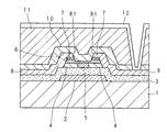
- FIG. 3 is a schematic diagram schematically illustrating an example of a thin film transistor used for a driving circuit and a pixel of the television receiver according to the first embodiment. It is principal part sectional drawing by the II line
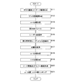
- FIG. 1 is a manufacturing process figure which shows an example of the manufacturing method of the pixel thin-film transistor of the television receiver which concerns on this Embodiment 1.
- FIG. 8 is a cross-sectional view of main parts taken along line IV-IV in FIG. 7. It is a schematic diagram which shows typically an example of the pixel thin-film transistor used for the pixel of the television receiver which concerns on this Embodiment 3.
- FIG. 10 is a cross-sectional view of a principal part taken along line VI-VI in FIG. 9.
- FIG. 12 is a cross-sectional view of a principal part taken along line VII-VII in FIG. It is a schematic diagram which shows typically an example of the pixel thin-film transistor used for the pixel of the television receiver which concerns on this Embodiment 5.
- FIG. It is a graph explaining the relationship between laser annealing integrated energy density and mobility. It is a graph which shows the electric current value change at the time of ON / OFF in the case where it comprises so that the electrical characteristic of a 1st channel area
- FIG. 1 is a functional block diagram showing a main configuration of the television receiver 100 according to the first embodiment.
- the television receiver 100 includes a TVSoC (System on Chip) 10 (transmission unit), a Tcon (Timing Controller) 20 that receives data from the TVSoC 10, and a source driver 30 and a gate driver 40 that receive data from the Tcon 20.
- the source driver 30 and the gate driver 40 are connected to a liquid crystal display panel 50 on which an image is displayed based on such data.
- the drive circuit described in the claims is, for example, the source driver 30 or the gate driver 40.
- the TVSoC 10 is a so-called television receiving circuit, receives a CVBS signal, an HDMI (registered trademark) signal, etc., generates a television image, and outputs an image signal including a television image signal, a horizontal synchronization signal, a vertical synchronization signal, and a clock, for example, Output to Tcon 20 using the V-by-One signal standard.
- the Tcon 20 generates a digital image signal, a control signal for controlling the operation of the drive circuit of the liquid crystal display panel 50, and the like based on the signal from the TVSoC 10.
- the Tcon 20 transmits the digital image signal and the control signal to the source driver 30 and the gate driver 40. That is, the Tcon 20 uses a timing signal such as a vertical synchronization signal, a horizontal synchronization signal, a data enable signal, and a clock signal from the TVSoC 10 to control the operation timing of the source driver 30 and the operation of the gate driver 40.
- a gate timing control signal for controlling the timing is generated.
- Tcon 20 and the source driver 30 are connected by, for example, 24 buses.
- Each pixel (picture element) (not shown) of the liquid crystal display panel 50 is connected to the source driver 30 and the gate driver 40 via the source line and the gate line.
- FIG. 2 is a schematic diagram schematically showing an example of a driving circuit and a thin film transistor (also referred to as a TFT) used in the pixel of the television receiver 100 according to the first embodiment.
- 2A shows a thin film transistor (hereinafter referred to as a pixel thin film transistor) used in a pixel of the television receiver 100
- FIG. 2B shows a thin film transistor (hereinafter referred to as a drive circuit thin film transistor) used in a drive circuit (peripheral circuit) of the television receiver 100. It is called).
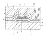
- FIG. 3 is a cross-sectional view of main parts taken along line II in FIG. 2A
- FIG. 4 is a cross-sectional view of main parts taken along line II-II in FIG. 2B.
- each thin film transistor has a gate electrode 2 laminated on the surface of a glass substrate 1 (also referred to as a substrate), and covers the gate electrode 2 to form a gate insulating film 3 (for example, SiO 2). Film, SiO 2 / SiN film stack, SiN film, SiON film, etc.).
- a polysilicon layer 5 (also referred to as a p-Si film).
- a first amorphous silicon layer 4 (also referred to as an a-Si film) is formed so as to surround the polysilicon layer 5 (polysilicon region), and covers the polysilicon layer 5 and the first amorphous silicon layer 4.
- a second amorphous silicon layer 6 (also referred to as an a-Si film) is laminated.
- the first amorphous silicon layer 4 and the second amorphous silicon layer 6 are collectively referred to as an amorphous silicon layer.
- n + silicon layer 7 (n + Si film) is laminated at a required position on the surface of the second amorphous silicon layer 6.
- the n + silicon layer 7 is a contact layer with the source electrode 8 and the drain electrode 9 and is a semiconductor layer having a high impurity concentration such as phosphorus.
- a source electrode 8 and a drain electrode 9 having a required pattern are formed on the surface of the n + silicon layer 7, the side surfaces of the second amorphous silicon layer 6 and the first amorphous silicon layer 4, and the surface of the gate insulating film 3. is there.
- the first amorphous silicon layer 4 and the second amorphous silicon layer 6 have a large resistance and a small off current (leakage current).
- the polysilicon layer 5 has much higher electron mobility than the amorphous silicon layer.
- the source electrode 8 and the drain electrode 9 are spaced apart from each other with a predetermined interval so that one end of each of the source electrode 8 and the drain electrode 9 is opposed to each other.
- the space between the source electrode 8 and the drain electrode 9 corresponds to a so-called channel region. Or movement of holes) occurs. That is, such a channel region is a portion corresponding to the interval between the source electrode 8 and the drain electrode 9 in the stacking direction, and the polysilicon layer 5, the first amorphous silicon layer 4, and the second amorphous silicon layer. 6.
- first thin film transistor a channel region related to the pixel thin film transistor
- second thin film transistor a channel region related to the driving circuit thin film transistor
- a passivation film 10 made of, for example, SiN is formed on the entire TFT so as to cover the source electrode 8 and the drain electrode 9, and an organic film 11 is formed on the surface of the passivation film 10 to cover the surface. It is flattened.
- a through hole is formed at a required position of the passivation film 10 and the organic film 11, and the pixel electrode 12 and the drain electrode 9 are electrically connected through the through hole.
- the pixel electrode 12 is formed of a transparent conductive film (for example, ITO).
- 2A and 2B schematically show a projected state in which the first amorphous silicon layer 4, the polysilicon layer 5, the source electrode 8 and the drain electrode 9 are projected onto the surface of the substrate 1.
- 2A and 2B, the second amorphous silicon layer 6 and other configurations are not shown for convenience of explanation.
- the first channel region C1 and the second channel region C2 are configured to have different electrical characteristics. This will be described in detail below.
- the first channel region C1 is configured to include an amorphous silicon region and a polysilicon region. That is, in the pixel thin film transistor, a region related to the first amorphous silicon layer 4 and a region related to the polysilicon layer 5 are formed in a portion corresponding to the distance between the source electrode 8 and the drain electrode 9 in the first channel region C1. Both are mixed.
- the polysilicon layer 5 which is a rectangular region as viewed in the drawing is formed at two locations, and is separated along the separation direction of the source electrode 8 and the drain electrode 9. In other words, the polysilicon layer 5 is formed at two locations in the first amorphous silicon layer 4 as viewed in FIG. 2A.
- the drawing direction, the separation direction (or the juxtaposition direction) of the two polysilicon layers 5 is referred to as a horizontal direction, and the direction orthogonal to the separation direction is referred to as a vertical direction.
- one polysilicon layer 5 overlaps the end 81 of the source electrode 8 in the stacking direction, and the other polysilicon layer 5 is stacked in the stacking direction. It overlaps with the end 91 of the drain electrode 9.
- the vertical dimension d of the two polysilicon layers 5 is larger than the vertical dimension W of the source electrode 8 and the drain electrode 9.
- a first amorphous silicon layer 4 is interposed between the two polysilicon layers 5.
- the two polysilicon layers 5 are separated from each other, and the first amorphous silicon layer 4 is interposed therebetween. That is, as the first channel region C1, since the region of the amorphous silicon layer 4 having a large resistance is interposed between the regions of the polysilicon layer 5, the off-current is smaller than that in the case where the first amorphous silicon layer 4 is not interposed. Can be reliably suppressed. On the other hand, since a part of each polysilicon layer 5 and the opposite end portions 81 and 91 of the source electrode 8 and the drain electrode 9 are overlapped in the direction of the lamination, a decrease in on-current is suppressed. You can also
- the amorphous silicon layer is formed around the polysilicon layer 5 and has a first amorphous silicon layer 4 having the same thickness as the polysilicon layer 5, the polysilicon layer 5, and the first layer. And a second amorphous silicon layer 6 formed on the surface of one amorphous silicon layer 4.
- the second amorphous silicon layer 6 is for preventing the source electrode 8 and the drain electrode 9 from directly contacting the channel region, and uses a characteristic with a small off-current (leakage current). Thereby, the off-current can be further reduced.
- the second channel region C2 is configured to include only the polysilicon region. That is, in the driving circuit thin film transistor, the amorphous silicon region does not exist in the portion corresponding to the distance between the source electrode 8 and the drain electrode 9 in the second channel region C2.
- the polysilicon layer 5 is formed in the first amorphous silicon layer 4 over the opposing end portions 81 and 91 of the source electrode 8 and the drain electrode 9 in the second channel region C2. It is formed in a wider area.
- the region of the polysilicon layer 5 having a resistance lower than that of the first amorphous silicon layer 4 extends over the opposite end portions 81 and 91 of the source electrode 8 and the drain electrode 9.
- the second channel region C2 consists only of the region of the polysilicon layer 5
- the on-current can be reliably increased as compared with the case where the first amorphous silicon layer 4 is present. it can.
- a part of the polysilicon layer 5 and the opposite end portions 81 and 91 of the source electrode 8 and the drain electrode 9 are overlapped in the stacking direction, so that the increase in on-current can be further increased. it can.
- first channel region C1 and the second channel region C2 are shown, but this defines the first channel region C1 and the second channel region C2 according to the present invention. It is not something.
- such a channel region depends on a channel length that is a distance between the drain electrode 9 and the source electrode 8 and a channel width that is a dimension of the drain electrode 9 and the source electrode 8 in a direction orthogonal to the channel length. Can be defined.
- FIG. 5 is a manufacturing process diagram showing an example of a manufacturing method of the pixel thin film transistor of the television receiver 100 according to the first embodiment.
- the manufacturing process of the pixel thin film transistor of the first embodiment will be described.
- the gate electrode 2 is formed on the glass substrate 1 (S11), and the gate insulating film 3 is formed on the surface of the glass substrate 1 so as to cover the gate electrode 2 (S12).
- a-Si film 4 as a first amorphous silicon layer is formed on the surface of the glass substrate 1 on which the gate insulating film 3 is formed (S13). Thereafter, a step of forming a channel region (first channel region C1) is performed, and the region of the polysilicon layer 5 is selectively formed in the first channel region C1 as described above.
- a dehydrogenation annealing process is performed (S14), and laser pre-cleaning is performed (S15).
- the a-Si film 4 is crystallized by a partial irradiation type laser (S16).
- the crystallization process is an annealing process (also referred to as a laser annealing process).
- a required part of the a-Si film 4 is irradiated with an energy beam through a multi-lens array, and the required part is exposed to the polysilicon layer 5 ( p-Si film).
- the required part is the upper side of the gate electrode 2 and the first channel region C1 between the source and the drain.
- two spaced apart polysilicon layers 5 are formed in the first amorphous silicon layer 4 as shown in FIG. 2A.
- the energy beam for example, an ultraviolet excimer laser having a large absorption of an amorphous silicon layer (a-Si film) can be used.
- FIG. 6 is a schematic diagram showing an example of the configuration of the partial irradiation laser according to the present embodiment.
- the glass substrate 1 on which the a-Si film 4 is formed is placed on a placing table (not shown) and is translated in the direction of the arrow in FIG. 6 at a required speed. It is.
- a multi-lens array is arranged in which individual lenses are arranged at an appropriate distance along a direction intersecting the moving direction of the glass substrate 1.
- the laser light is partially irradiated to a plurality of required locations separated via different optical paths for each lens. That is, partial laser annealing can be performed. Thereby, only a required region of the channel region in the a-Si film 4 is selectively changed to the polysilicon layer 5 (p-Si film).
- n + Si film (n + silicon layer) 7 is formed on the surface of the a-Si film 6 (S19).
- the n + Si film 7 is a contact layer with the source electrode 8 and the drain electrode 9 and is a semiconductor layer having a high impurity concentration such as phosphorus.
- the a-Si film 4, the a-Si film 6, and the n + Si film 7 are etched to form, for example, a rectangular island shape.
- a metal for source / drain is formed on the n + Si film 7, and the metal film is etched to form the source electrode 8 and the drain electrode 9 (S20).
- the a-Si film 6 is formed in the thickness direction with respect to the n + Si film 7 and the a-Si film 6 related to the channel portion using the source electrode 8 and the drain electrode 9 as a mask. Etching is performed halfway (S21). As a result, a channel region is formed.
- the step of forming the a-Si film 4, the a-Si film 6, and the n + Si film 7 is formed in an island shape, but the present invention is not limited to this.
- the source / drain metal film is etched in a predetermined pattern, and then the n + Si film 7 and the a-Si film 6 are etched in the thickness direction. You may make it give.
- an energy beam for example, a laser
- an energy beam is not irradiated on the entire surface of the substrate, but an energy beam is applied only to a region of the a-Si film 4 that is to become the polysilicon layer 5.
- the first channel region C1 can be formed only by partial irradiation and annealing. Therefore, in order to form the first channel region C1, a crystallized polysilicon layer is formed on the entire substrate surface, and the steps of exposure processing, development processing, and etching processing are not required for the polysilicon layer. The manufacturing process can be shortened.
- the a-Si film 4 is selectively crystallized with a partial irradiation type laser as shown in FIG. 5 has been described as an example for the pixel thin film transistor. It is not limited. Such a crystallization process may be performed on the driving circuit thin film transistor.
- the first channel region C1 and the second channel region C2 have different electrical characteristics, and the pixel thin film transistor is It operates as a transistor suitable for the pixel on which the image is displayed, and the driving circuit thin film transistor operates as a transistor suitable for the driving circuit of the pixel.
- the pixel thin film transistor (the first channel region C1) has the above-described configuration, so that the off current can be reliably suppressed while suppressing the decrease in the on current. Can be suppressed.
- the drive circuit thin film transistor (second channel region C2) has the above-described configuration, so that the on-current can be reliably increased. it can.
- the present invention is not limited to the description of the first embodiment.
- the configuration of the pixel thin film transistor (first channel region C1) is different from that of the first embodiment, as in the first embodiment, the first channel region C1 and The second channel region C2 is configured to have different electrical characteristics. This will be described in detail below.
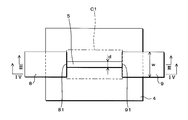
- FIG. 7 is a schematic diagram schematically showing an example of a pixel thin film transistor used for a pixel of the television receiver 100 according to the second embodiment
- FIG. 8 is a cross-sectional view taken along line IV-IV in FIG. is there. 7 is the same as FIG. 4 and is omitted.
- the drive circuit thin film transistor according to the second embodiment is the same as that of the first embodiment, and a detailed description thereof is omitted.
- the first channel region C1 is configured to include an amorphous silicon region and a polysilicon region. That is, in the pixel thin film transistor, both the region related to the amorphous silicon layer 4 and the region related to the polysilicon layer 5 coexist in the portion corresponding to the distance between the source electrode 8 and the drain electrode 9 in the first channel region C1. It is.
- the polysilicon layer 5 is elongated in the lateral direction from the end 81 of the source electrode 8 to the end 91 of the drain electrode 9. Is formed.
- the region related to the polysilicon layer 5 has a strip shape as viewed in the drawing, and one of the ends of the polysilicon layer 5 overlaps the end portion 81 of the source electrode 8 in the stacking direction. The other overlaps the end 91 of the drain electrode 9 in the stacking direction. More specifically, both end portions of the polysilicon layer 5 overlap with the end portion 81 of the source electrode 8 or the end portion 91 of the drain electrode 9 at the intermediate portion between the source electrode 8 and the drain electrode 9 in the vertical direction.
- the vertical dimension d of the polysilicon layer 5 is smaller than the vertical dimension W of the source electrode 8 and the drain electrode 9, and both ends of the polysilicon layer 5 are located on the source electrode 8 in the stacking direction.
- the end portion 81 and the end portion 91 of the drain electrode 9 partially overlap each other.
- the pixel thin film transistor (first channel region C1) has the above-described configuration, it is suitable for a pixel thin film transistor that needs to reduce off-current. Operates as a transistor.
- the first channel region C 1 is adjacent to the source electrode 8 and the drain electrode 9.
- the region or a nearby region can be the amorphous silicon layer 4, and off current can be suppressed.
- the present invention is not limited to the description in the first and second embodiments.
- the configuration of the pixel thin film transistor (first channel region C1) is different from that of the first and second embodiments, the first and second similar to the first and second embodiments.
- the channel region C1 and the second channel region C2 are configured to have different electrical characteristics. This will be described in detail below.
- FIG. 9 is a schematic diagram schematically illustrating an example of a pixel thin film transistor used for a pixel of the television receiver 100 according to the third embodiment
- FIG. 10 is a cross-sectional view of a principal part taken along line VI-VI in FIG. is there. 9 is the same as FIG. 4 and is omitted.
- the drive circuit thin film transistor according to the third embodiment is the same as that of the first embodiment, and a detailed description thereof is omitted.
- the first channel region C1 is configured to include an amorphous silicon region and a polysilicon region. That is, in the pixel thin film transistor, both the region related to the amorphous silicon layer 4 and the region related to the polysilicon layer 5 coexist in the portion corresponding to the distance between the source electrode 8 and the drain electrode 9 in the first channel region C1. It is.
- the polysilicon layer 5 is elongated in the lateral direction from the end 81 of the source electrode 8 to the end 91 of the drain electrode 9. Is formed. Further, the polysilicon layer 5 is formed in the middle portion in the lateral direction, in other words, in the middle between the opposing end portions 81 and 91 of the source electrode 8 and the drain electrode 9 so as to have a size that is increased in the vertical direction. ing.
- the region related to the polysilicon layer 5 has a cross shape as viewed in the drawing, and one of the ends of the polysilicon layer 5 along the horizontal direction is the end portion 81 of the source electrode 8 in the stacking direction.
- the other overlaps the end 91 of the drain electrode 9 in the stacking direction. More specifically, both end portions of the polysilicon layer 5 along the horizontal direction are respectively connected to the end portion 81 of the source electrode 8 or the end portion 91 of the drain electrode 9 at the intermediate portion between the source electrode 8 and the drain electrode 9 in the vertical direction. overlapping.
- the vertical dimension d1 of the polysilicon layer 5 is smaller than the vertical dimension W of the source electrode 8 and the drain electrode 9, and both ends of the polysilicon layer 5 along the horizontal direction are in the direction of the stacking. It partially overlaps the end portion 81 of the source electrode 8 and the end portion 91 of the drain electrode 9. Also, in the portion extending in the vertical direction of the polysilicon layer 5, the horizontal dimension d ⁇ b> 2 may be configured to be smaller than the vertical dimension W of the source electrode 8 and the drain electrode 9.
- first channel region C1 Since such a pixel thin film transistor (first channel region C1) has the above-described configuration, it is suitable for a pixel thin film transistor that needs to reduce off-current. Operates as a transistor.
- the polysilicon layer 5 is adjacent to the source electrode 8 and the drain electrode 9 in the first channel region C1.
- the region or a nearby region can be the amorphous silicon layer 4, and off current can be suppressed.
- the vertical dimension d1 of the polysilicon layer 5 is enlarged at the middle portion of the polysilicon layer 5 in the horizontal direction. Accordingly, an increase in on-current can be achieved.
- the present invention is not limited to the description of the first to third embodiments.
- the configuration of the pixel thin film transistor (first channel region C1) is different from that of the first to third embodiments, the first thin film transistor 100 is similar to the first to third embodiments.
- the channel region C1 and the second channel region C2 are configured to have different electrical characteristics. This will be described in detail below.
- FIG. 11 is a schematic diagram schematically showing an example of a pixel thin film transistor used for a pixel of the television receiver 100 according to the fourth embodiment
- FIG. 12 is a cross-sectional view of a principal part taken along line VII-VII in FIG. is there.
- the drive circuit thin film transistor according to the fourth embodiment is the same as that of the first embodiment, and a detailed description thereof is omitted.
- the first channel region C1 is configured to include an amorphous silicon region and a polysilicon region. That is, in the pixel thin film transistor, both the region related to the amorphous silicon layer 4 and the region related to the polysilicon layer 5 coexist in the portion corresponding to the distance between the source electrode 8 and the drain electrode 9 in the first channel region C1. It is.
- the polysilicon layer 5 is located at one location between the end portion 81 of the source electrode 8 and the end portion 91 of the drain electrode 9. Is formed.
- the region related to the polysilicon layer 5 has a rectangular shape, and the end 81 of the source electrode 8 and the end of the drain electrode 9 are between the end 81 of the source electrode 8 and the end 91 of the drain electrode 9. It is formed away from the portion 91.
- the vertical dimension d of the polysilicon layer 5 is larger than the vertical dimension W of the source electrode 8 and the drain electrode 9, but the polysilicon layer 5 has the end 81 of the source electrode 8 and the drain electrode 9 in the stacking direction. It does not overlap with the end portion 91.
- first channel region C1 since such a pixel thin film transistor (first channel region C1) has the above-described configuration, it is suitable for a pixel thin film transistor that needs to reduce off-current. Operates as a transistor.
- the region related to the polysilicon layer 5 includes the end 81 of the source electrode 8 and the drain electrode across the region related to the first amorphous silicon layer 4.
- Nine end portions 91 are formed. That is, the region of the amorphous silicon layer 4 having a high resistance is formed between the region related to the polysilicon layer 5 and the end portion 81 of the source electrode 8 and the end portion 91 of the drain electrode 9. Accordingly, in the first channel region C1, the region adjacent to or near the source electrode 8 and the drain electrode 9 can be the amorphous silicon layer 4, and the off-current can be suppressed.
- Embodiment 5 The present invention is not limited to the description of Embodiments 1 to 4.
- the configuration of the pixel thin film transistor (first channel region C1) is different from that of the first to fourth embodiments, the first thin film transistor 100 is similar to the first to fourth embodiments.
- the channel region C1 and the second channel region C2 are configured to have different electrical characteristics. This will be described in detail below.
- FIG. 13 is a schematic diagram schematically showing an example of a pixel thin film transistor used for a pixel of the television receiver 100 according to the fifth embodiment.
- a cross-sectional view taken along line VIII-VIII in FIG. This is the same, and illustration is omitted.
- the drive circuit thin film transistor according to the fourth embodiment is the same as that of the first embodiment (FIG. 2B), and a detailed description thereof is omitted.
- the first channel region C1 and the second channel region C2 that is, the end 81 of the source electrode 8 and the end of the drain electrode 9 are provided. Only a region related to the polysilicon layer 5 is formed in a portion corresponding to the interval between the portions 91.
- the polysilicon layer 5 is configured to have different crystallinity. Yes.
- the polysilicon layer of the first channel region C1 5 is formed with a low crystallinity
- the polysilicon layer 5 in the second channel region C2 is formed with a high crystallinity (at least higher than the first channel region C1).
- the halftone mask is a mask having, for example, a semi-transmissive portion different from the light transmittance of the transmissive portion and the transmittance of the light-shielded portion in addition to the laser light transmissive portion and the light-shielded portion.
- the mobility of electrons (or holes) in the first channel region C1 and the second channel region C2 can be appropriately controlled.
- FIG. 14 is a graph illustrating the relationship between the laser annealing integrated energy density and mobility.
- the laser annealing integrated energy density is high, that is, when the high laser annealing integrated energy density is increased during laser annealing of amorphous silicon, the crystallinity of polysilicon is increased.
- the laser annealing integrated energy density is a value obtained by multiplying the laser power density by the number of times of irradiation.
- the television receiver 100 is configured such that the electron mobility (electrical characteristics) in the first channel region C1 and the second channel region C2 are different,
- the pixel thin film transistor operates as a transistor suitable for a pixel on which an image is displayed, and the driving circuit thin film transistor operates as a transistor suitable for the driving circuit of the pixel.
- the crystallinity of the polysilicon layer 5 in the first channel region C1 is lowered, so that the off-current can be reliably suppressed.
- the drive circuit peripheral circuit
- the crystallinity of the polysilicon layer 5 in the second channel region C2 is increased, the on-current can be reliably increased.
- FIG. 15 is a graph showing a change in current value at ON / OFF when the first channel region C1 and the second channel region C2 are configured to have different electrical characteristics as described above. That is, FIG. 15 shows a so-called TFT characteristic curve.
- a solid line indicates a thin film transistor made of only amorphous silicon (a-Si)
- a thick line indicates a pixel thin film transistor
- a dotted line indicates a drive circuit thin film transistor.
- the drive circuit thin film transistor has a high current value at the on / off time.
- the current value at the on / off time is significantly lower than that in the case of the driving circuit thin film transistor.
- the pixel thin film transistor has a higher on-state current value than a thin film transistor made of only amorphous silicon.
- the electrical characteristics of the first channel region C1 and the second channel region C2 are different by crystallizing the a-Si film 4 with a partial irradiation laser for the pixel thin film transistor or the drive circuit thin film transistor.
- the case where it is configured as described above has been described as an example. However, the present invention is not limited to this.
- the channel region may be formed by performing each process step.
Landscapes
- Physics & Mathematics (AREA)
- Nonlinear Science (AREA)
- Chemical & Material Sciences (AREA)
- Crystallography & Structural Chemistry (AREA)
- Mathematical Physics (AREA)
- General Physics & Mathematics (AREA)
- Optics & Photonics (AREA)
- Engineering & Computer Science (AREA)
- Microelectronics & Electronic Packaging (AREA)
- Thin Film Transistor (AREA)
- Liquid Crystal (AREA)
- Devices For Indicating Variable Information By Combining Individual Elements (AREA)
- Recrystallisation Techniques (AREA)
Abstract
第1薄膜トランジスを有する絵素と、第2薄膜トランジスタを有し、前記絵素を駆動する駆動回路とを備える表示装置において、前記第1薄膜トランジスタに係る第1チャネル領域、及び、前記第2薄膜トランジスタに係る第2チャネル領域が、電気的特性(例えば、電子移動度)が相違するように構成することにより、第1薄膜トランジス及び第2薄膜トランジスタが夫々の役割に適した作動ができる表示装置及び該表示装置の製造方法を提供する。
Description
本発明は、第1薄膜トランジスを有する絵素と、第2薄膜トランジスタを有し、前記絵素を駆動する駆動回路とを備える表示装置及び該表示装置の製造方法に関する。
近年、液晶パネル等を有する表示装置においては、薄膜トランジスタ(TFT:Thin Film Transistor)が主に用いられる。具体的には、アモルファスシリコン(amorphous silicon)をチャネル領域に用いたa-Si TFT、又はポリシリコン(poly-crystalline silicon)をチャネル領域に用いたP-Si TFTが用いられる。また、P-Si TFTは、基板全面にレーザーを照射後、パターニングを行うレーザーアニール方式により製造される。
特許文献1には、ゲート電極を覆うように形成されたゲート絶縁膜と、前記ゲート絶縁膜の上に形成されたポリシリコン膜と、前記ポリシリコン膜の端部の上方に形成されたソース電極と、前記ポリシリコン膜における前記ソース電極が形成された端部と対向する端部の上方に形成され、前記ソース電極と離間しているドレイン電極とを具備する薄膜トランジスタにおいて、前記ポリシリコン膜におけるソース電極又はドレイン電極が形成されている前記ポリシリコン膜の端部から、前記ポリシリコン膜におけるソース電極又はドレイン電極が形成されていない前記ポリシリコン膜の中央部に向かって、前記ポリシリコン膜の結晶化率が小さくなることについて開示されている。
一方、ピクセル(絵素)を駆動する周辺回路又は駆動回路は、回路として駆動する為に高いオン電流が要求される。一方、ピクセルでは頻繁にオン・オフのスイッチングが行われることから、オフ電流が低い方が望ましい。
これに対して、上述したP-Si TFTは、オン時に流れる電流(オン電流)、及び、オフ時に流れる電流(オフ電流)が共に高いという特性を有している。従って、周辺回路又は駆動回路用のTFTには適しているものの、ピクセル用のTFTには好ましくない。
このように、同一基板上、又は同一装置内においても、その機能に応じて、電子移動度(電気的特性)の異なる複数種のTFTが要求されている。しかしながら、従来のレーザーアニール方式を用いて斯かる複数種のTFTを設けることは複雑な工程であり、手間の掛かるものである。また、このような問題に対して、特許文献1に係る薄膜トランジスタにおいては工夫も言及もされていない。
本発明は、斯かる事情に鑑みてなされたものであり、その目的とするところは、第1薄膜トランジスタを有する絵素と、第2薄膜トランジスタを有し、前記絵素を駆動する駆動回路とを備える表示装置において、前記第1薄膜トランジスタに係る第1チャネル領域、及び、前記第2薄膜トランジスタに係る第2チャネル領域が、電気的特性(例えば、電子移動度)が相違するように構成することにより、第1薄膜トランジス及び第2薄膜トランジスタが夫々の役割に適した作動ができる表示装置及び該表示装置の製造方法を提供することにある。
本発明に係る表示装置は、第1薄膜トランジスタを有する絵素と、第2薄膜トランジスタを有し、前記絵素を駆動する駆動回路とを備える表示装置において、前記第1薄膜トランジスタは第1チャネル領域を有し、前記第2薄膜トランジスタは第2チャネル領域を有しており、前記第1チャネル領域はアモルファスシリコン領域及びポリシリコン領域を含み、前記第1チャネル領域及び前記第2チャネル領域は、電気的特性が相違することを特徴とする。
本発明にあっては、例えば、前記第1チャネル領域はアモルファスシリコン領域及びポリシリコン領域を含み、前記第2チャネル領域はポリシリコン領域のみを含むように構成することにより、前記第1チャネル領域及び前記第2チャネル領域において、電気的特性が相違するように構成する。
本発明に係る表示装置は、前記第1薄膜トランジスタでは、ゲート電極の上側に、前記第1チャネル領域を挟んで、ソース電極及びドレイン電極が所定の間隔を離れて積層されており、前記第1チャネル領域には、アモルファスシリコン領域及びポリシリコン領域が混在してあることを特徴とする。
本発明にあっては、前記第1薄膜トランジスタでは、前記第1チャネル領域にアモルファスシリコン領域及びポリシリコン領域が混在してある。
本発明に係る表示装置は、前記ポリシリコン領域は離隔された2ヶ所であり、一方のポリシリコン領域は、前記積層の方向にて、前記ソース電極と重なっており、他方のポリシリコン領域は、前記積層の方向において、前記ドレイン電極と重なっていることを特徴とする。
本発明にあっては、前記2ヶ所のポリシリコン領域うち一方のポリシリコン領域は、前記積層の方向にて、前記ソース電極と重なっており、他方のポリシリコン領域は、前記積層の方向において、前記ドレイン電極と重なっている。換言すれば、前記2ヶ所のポリシリコン領域は夫々ソース電極及びドレイン電極周囲に形成されている。
本発明に係る表示装置は、前記ポリシリコン領域は前記ソース電極及び前記ドレイン電極の離隔の方向に長く、前記ポリシリコン領域の両端側が、前記積層の方向にて、前記ソース電極及び前記ドレイン電極の両対向端の一部と夫々重なっていることを特徴とする。
本発明にあっては、前記ポリシリコン領域の両端側が、前記積層の方向にて、前記ソース電極及び前記ドレイン電極の両対向端の一部と夫々重なっており、前記ソース電極及び前記ドレイン電極に隣接する領域又は近傍の領域をアモルファスシリコン領域とする。
本発明に係る表示装置は、前記ポリシリコン領域は、前記ソース電極及び前記ドレイン電極の両対向端の中間にて、前記離隔の方向と直交する方向の寸法が大きくなることを特徴とする。
本発明にあっては、前記ポリシリコン領域は斯かる両端側が、前記積層の方向にて、前記ソース電極及び前記ドレイン電極の両対向端の一部と夫々重なっており、前記ソース電極及び前記ドレイン電極の両対向端の中間にて、前記離隔の方向と直交する方向の寸法が大きくなる。従って、前記ソース電極及び前記ドレイン電極に隣接する領域又は近傍の領域がアモルファスシリコン領域となる。
本発明に係る表示装置は、前記ポリシリコン領域は1ヶ所であって、前記ソース電極及び前記ドレイン電極の両対向端の間に介在し、前記積層の方向にて、前記ソース電極及び前記ドレイン電極の両対向端と重なっていないことを特徴とする。
本発明にあっては、前記積層の方向にて、前記ソース電極及び前記ドレイン電極の両対向端と重ならないように、前記ポリシリコン領域が、前記ソース電極及び前記ドレイン電極の両対向端の間に介在し、前記ソース電極及び前記ドレイン電極に隣接する領域又は近傍の領域をアモルファスシリコン領域とする。
本発明に係る表示装置は、前記第1薄膜トランジスタ及び前記第2薄膜トランジスタ夫々は、ゲート電極の上側に、前記第1チャネル領域又は前記第2チャネル領域を挟んで、ソース電極及びドレイン電極が所定の間隔を離れて積層されており、前記第1チャネル領域及び前記第2チャネル領域にはポリシリコン領域のみが存在し、前記第1チャネル領域と、前記第2のチャネル領域とは、ポリシリコンの結晶性が異なることを特徴とする。
本発明にあっては、前記第1チャネル領域及び前記第2チャネル領域にはポリシリコン領域のみが存在し、前記第1チャネル領域と、前記第2のチャネル領域とは、ポリシリコンの結晶性が異なる。
本発明に係る表示装置の製造方法は、第1薄膜トランジスタを有する複数の画素と、第2薄膜トランジスタを有し、該画素を駆動する駆動回路とを備える表示装置の製造方法において、複数のゲート電極に係るゲート電極絶縁層を形成する工程と、該ゲート電極絶縁層の上にアモルファスシリコン層を形成する工程と、前記第1薄膜トランジスタに係る第1チャネル領域を形成するチャネル工程を含み、前記チャネル工程では、前記アモルファスシリコン層にポリシリコン領域が選択的に形成されることを特徴とする。
本発明にあっては、複数のゲート電極に係るゲート電極絶縁層が形成された後、該ゲート電極絶縁層の上にアモルファスシリコン層が形成され、以後、該アモルファスシリコン層にポリシリコン領域が選択的に形成されて、前記第1薄膜トランジスタに係る第1チャネル領域が形成される。
本発明に係る表示装置の製造方法は、前記チャネル工程では前記アモルファスシリコン層にエネルギービームを部分的に照射してポリシリコン層に変化させるアニール工程と、前記ポリシリコン層を覆って他のアモルファスシリコン層を形成する工程と、前記他のアモルファスシリコン層の表面にn+シリコン層を形成する工程とを含むことを特徴とする。
本発明にあっては、前記チャネル工程で、前記アモルファスシリコン層にエネルギービームを部分的に照射してポリシリコン層に変化させた後、前記ポリシリコン層を覆って他のアモルファスシリコン層が形成され、該他のアモルファスシリコン層の表面にn+シリコン層が形成される。
本発明によれば、オフ電流を下げる必要のあるピクセル(絵素)に対しては、前記第1薄膜トランジスタがオフ電流を確実に抑えることができ、オン電流を高める必要のある駆動回路(周辺回路)に対しては、前記第2薄膜トランジスタがオン電流を確実に高めることができるので、前記第1薄膜トランジス及び前記第2薄膜トランジスタが夫々の役割に適した作動を行うことが出来る。
以下に、本発明の実施の形態に係る表示装置及び該表示装置の製造方法を、いわゆる液晶パネルを有するテレビジョン受信機に適用した場合を例として、図面に基づいて詳述する。
(実施の形態1)
図1は実施の形態1のテレビジョン受信機100の要部構成を示す機能ブロック図である。
図1は実施の形態1のテレビジョン受信機100の要部構成を示す機能ブロック図である。
テレビジョン受信機100は、TVSoC(System on a Chip)10(送信部)と、TVSoC10からデータを受信するTcon(Timing Controller)20と、更にTcon20からデータを受信するソースドライバ30及びゲートドライバ40とを備えており、ソースドライバ30及びゲートドライバ40は斯かるデータに基づいて画像が表示される液晶表示パネル50に接続されている。
請求の範囲に記載の駆動回路は、例えば、ソースドライバ30又はゲートドライバ40である。
TVSoC10はいわゆるテレビ受信回路であり、CVBS信号,HDMI(登録商標)信号などを受け取ってテレビ映像を生成し、テレビ画像信号,水平同期信号,垂直同期信号,及びクロックを含む画像信号を、例えば、V-by-One信号規格を用いてTcon20に出力する。
Tcon20は、TVSoC10からの信号に基づいて、デジタル画像信号、液晶表示パネル50の駆動回路の動作を制御するための制御信号等を生成する。そして、Tcon20は、デジタル画像信号及び制御信号をソースドライバ30及びゲートドライバ40に送信する。すなわちTcon20は、TVSoC10から垂直同期信号、水平同期信号、データイネーブル信号、クロック信号などのタイミング信号を用いて、ソースドライバ30の動作タイミングを制御するためのソースタイミング制御信号と、ゲートドライバ40の動作タイミングを制御するためのゲートタイミング制御信号を発生する。
また、Tcon20及びソースドライバ30の間は、例えば24本のバスによって接続されている。
液晶表示パネル50の図示しない各ピクセル(絵素)は、ソースライン及びゲートラインを介して、ソースドライバ30及びゲートドライバ40に接続されている。
図2は本実施の形態1に係るテレビジョン受信機100の駆動回路及びピクセルに用いられる薄膜トランジスタ(TFTとも称する)の一例を模式的に示す模式図である。図2Aはテレビジョン受信機100のピクセルに用いられる薄膜トランジスタ(以下、ピクセル薄膜トランジスタと称する)を示し、図2Bはテレビジョン受信機100の駆動回路(周辺回路)に用いられる薄膜トランジスタ(以下、駆動回路薄膜トランジスタと称する)を示している。
また、図3は図2AのI-I線による要部断面図であり、図4は図2BのII-II線による要部断面図である。
図3及び図4に示すように、夫々の薄膜トランジスタは、ガラス基板1(基板とも称する)の表面にゲート電極2を積層してあり、ゲート電極2を覆ってゲート絶縁膜3(例えば、SiO2 膜、SiO2 /SiN膜積層、SiN膜、SiON膜など)を積層してある。
また、図2~図4に示すように、ゲート絶縁膜3の表面であってゲート電極2の上側には、ポリシリコン層5(p-Si膜とも称する。なお、ポリシリコン層には多結晶だけでなく、多結晶よりも比較的結晶粒径の小さい微結晶、あるいは、より結晶性の高い単結晶も含む)を積層してある。また、ポリシリコン層5(ポリシリコン領域)を取り囲むように第1のアモルファスシリコン層4(a-Si膜とも称する)が形成され、ポリシリコン層5及び第1のアモルファスシリコン層4を覆うように第2のアモルファスシリコン層6(a-Si膜とも称する)を積層してある。以下においては、第1のアモルファスシリコン層4及び第2のアモルファスシリコン層6を纏めてアモルファスシリコン層とも称する。
第2のアモルファスシリコン層6の表面の所要位置には、n+シリコン層7(n+Si膜)を積層してある。n+シリコン層7は、ソース電極8及びドレイン電極9とのコンタクト層であり、リンなどの不純物濃度が高い半導体層である。
n+シリコン層7の表面、第2のアモルファスシリコン層6及び第1のアモルファスシリコン層4の側面、ゲート絶縁膜3の表面には、所要のパターンを有するソース電極8及びドレイン電極9を形成してある。
第1のアモルファスシリコン層4及び第2のアモルファスシリコン層6は、抵抗が大きくオフ電流(漏れ電流)が小さい。また、ポリシリコン層5は、アモルファスシリコン層に比べて電子の移動度が格段に大きい。
ソース電極8とドレイン電極9とは夫々の一端が対向するように、所定の間隔を挟んで離隔されており、ソース電極8とドレイン電極9との間はいわゆるチャネル領域に該当し、キャリア(電子又はホール)の移動が生じる。すなわち、斯かるチャネル領域は、前記積層方向において、ソース電極8とドレイン電極9との間隔に該当する部分であり、ポリシリコン層5と、第1のアモルファスシリコン層4及び第2のアモルファスシリコン層6とで構成されている。以下においては、前記ピクセル薄膜トランジスタ(第1薄膜トランジスタ)に係るチャネル領域を第1チャネル領域C1といい、前記駆動回路薄膜トランジスタ(第2薄膜トランジスタ)に係るチャネル領域を第2チャネル領域C2という。
ソース電極8及びドレイン電極9を覆うようにして、TFT全体には、例えば、SiNで構成されるパッシベーション膜10を形成してあり、パッシベーション膜10の表面には有機膜11を形成して表面を平坦化している。パッシベーション膜10及び有機膜11の所要の位置には、スルーホールを形成してあり、当該スルーホールを通して画素電極12とドレイン電極9とが導通するようにしてある。画素電極12は、透明導電膜(例えば、ITO)により形成されている。
図2A及び図2Bでは、第1のアモルファスシリコン層4、ポリシリコン層5、ソース電極8及びドレイン電極9を基板1の表面に射影した射影状態を模式的に示す。なお、図2A及び図2Bでは、説明の便宜上、第2のアモルファスシリコン層6及び他の構成の図示を省略している。
本実施の形態に係るテレビジョン受信機100においては、第1チャネル領域C1及び第2チャネル領域C2は、電気的特性が相違するように構成されている。以下、詳しく説明する。
前記ピクセル薄膜トランジスタにおいては、図2Aに示すように、第1チャネル領域C1がアモルファスシリコン領域及びポリシリコン領域を含むように構成されている。すなわち、前記ピクセル薄膜トランジスタでは、第1チャネル領域C1のうち、ソース電極8とドレイン電極9との間隔に対応する部分に、第1のアモルファスシリコン層4に係る領域及びポリシリコン層5に係る領域が共に混在してある。
図2Aのピクセル薄膜トランジスタにおいては、図面視、矩形の領域であるポリシリコン層5が夫々2ヶ所に形成されており、ソース電極8とドレイン電極9との離隔方向に沿って離隔されている。換言すれば、図2Aの図面視、第1のアモルファスシリコン層4内の離れた2ヶ所には、ポリシリコン層5が形成されている。
以下においては、説明の便宜上、図面視、2つのポリシリコン層5の離隔方向(又は並設方向)を横方向、該離隔方向に直交する方向を縦方向と称する。
2つのポリシリコン層5のうち、一方のポリシリコン層5は、前記積層の方向にて、ソース電極8の端部81と重なっており、他方のポリシリコン層5は、前記積層の方向において、ドレイン電極9の端部91と重なっている。
また、図2Aに示すように、前記2つのポリシリコン層5の縦方向の寸法dは、ソース電極8及びドレイン電極9の縦方向の寸法Wより大きい。一方、前記2つのポリシリコン層5の間には第1のアモルファスシリコン層4が介在している。
このように、2つのポリシリコン層5が夫々離隔され、これらの間には第1のアモルファスシリコン層4が介在する。すなわち、第1チャネル領域C1としては、抵抗が大きいアモルファスシリコン層4の領域がポリシリコン層5の領域の間に介在するので、第1のアモルファスシリコン層4が介在しない場合に比べて、オフ電流を確実に抑えることができる。一方、各ポリシリコン層5の一部と、ソース電極8及びドレイン電極9の相互対向する両端部81,91とが前記積層の方向にて重なるようにしてあるので、オン電流の低下を抑制することもできる。
また、図3に示すように、アモルファスシリコン層は、ポリシリコン層5の周囲に形成され、ポリシリコン層5と同程度の厚みを有する第1のアモルファスシリコン層4と、ポリシリコン層5及び第1のアモルファスシリコン層4の表面に形成された第2のアモルファスシリコン層6とを有する。
すなわち、ポリシリコン層5は、ゲート電極2の上側に形成された第1のアモルファスシリコン層4のうち、斯かるチャネル領域の一部の領域を多結晶状態であるポリシリコン層5に変化させたものであり、該チャネル領域を形成するために、露光、現像及びエッチング処理の各処理を行っていないことが分かる。また、第2のアモルファスシリコン層6は、ソース電極8及びドレイン電極9とチャネル領域とが直接接触しないようにするためのもので、オフ電流(漏れ電流)が小さい特性を用いている。これにより、オフ電流をより低減することができる。
一方、前記駆動回路薄膜トランジスタにおいては、図2Bに示すように、第2チャネル領域C2がポリシリコン領域のみを含むように構成されている。すなわち、前記駆動回路薄膜トランジスタでは、第2チャネル領域C2のうち、ソース電極8とドレイン電極9との間隔に対応する部分には、アモルファスシリコン領域が存在していない。
図2Bの駆動回路薄膜トランジスタにおいては、第1のアモルファスシリコン層4内に、ポリシリコン層5が、ソース電極8とドレイン電極9との両対向端部81,91に亘って、第2チャネル領域C2より広い領域にて形成されている。
このように、第2チャネル領域C2としては、第1のアモルファスシリコン層4に比べて抵抗が小さいポリシリコン層5の領域がソース電極8とドレイン電極9との両対向端部81,91に亘って形成されているので、換言すれば第2チャネル領域C2がポリシリコン層5の領域のみからなるので、第1のアモルファスシリコン層4が存在する場合に比べて、オン電流を確実に高めることができる。一方、ポリシリコン層5の一部と、ソース電極8及びドレイン電極9の対向する両端部81,91とが前記積層の方向にて重なるようにしてあるので、オン電流の増加を一層高めることができる。
図2A及び図2Bにおいては、説明の便宜上、第1チャネル領域C1及び第2チャネル領域C2を図示しているが、これによって本発明に係る第1チャネル領域C1及び第2チャネル領域C2が定義されるものでない。
また、一般に、斯かるチャネル領域は、ドレイン電極9及びソース電極8の間の距離であるチャネル長と、該チャネル長に直交する方向における、ドレイン電極9及びソース電極8の寸法であるチャネル幅によって定義することができる。
図5は本実施の形態1に係るテレビジョン受信機100のピクセル薄膜トランジスタの製造方法の一例を示す製造工程図である。以下、本実施の形態1のピクセル薄膜トランジスタの製造工程について説明する。図5に示すように、ガラス基板1上にゲート電極2を形成し(S11)、ゲート電極2を覆ってガラス基板1の表面にゲート絶縁膜3を形成する(S12)。
ゲート絶縁膜3が形成されたガラス基板1の表面に第1のアモルファスシリコン層としてのa-Si膜4を形成する(S13)。
以後、チャネル領域(第1チャネル領域C1)を形成する工程が行われ、上述したように、第1チャネル領域C1内にポリシリコン層5の領域を選択的に形成する。
以後、チャネル領域(第1チャネル領域C1)を形成する工程が行われ、上述したように、第1チャネル領域C1内にポリシリコン層5の領域を選択的に形成する。
まず、a-Si膜4をレーザーアニールするために、脱水素アニール処理を行い(S14)、レーザー前洗浄を行う(S15)。次に、部分照射型レーザーによるa-Si膜4の結晶化を行う(S16)。結晶化の工程は、アニール工程(レーザーアニール工程とも称する)であり、例えば、a-Si膜4の所要箇所にマルチレンズアレイを介してエネルギービームを照射して当該所要箇所をポリシリコン層5(p-Si膜)に変化させる。所要箇所は、ゲート電極2の上側であり、ソース・ドレイン間の第1チャネル領域C1である。これにより、第1のアモルファスシリコン層4に図2Aに示すように、離隔された2つのポリシリコン層5が形成される。エネルギービームは、例えば、アモルファスシリコン層(a-Si膜)の吸収の大きい紫外光のエキシマレーザーを用いることができる。
図6は本実施の形態に係る部分照射型レーザーの構成の一例を示す模式図である。図6に示すように、a-Si膜4が表面に形成されたガラス基板1は載置台(図示せず)に載置され、図6中の矢印の方向に所要の速度で平行移動するようにしてある。ガラス基板1の上方には、ガラス基板1の移動方向と交差する方向に沿って個々のレンズが適長離隔して並んだマルチレンズアレイを配置してある。レーザー光源(図示せず)からのレーザー光をマルチレンズアレイへ入射することにより、レーザー光は、レンズ毎に異なる光路を経由して離隔した複数の所要箇所に対して部分照射される。すなわち、部分レーザーアニールを行うことができる。これにより、a-Si膜4のうち、チャネル領域の所要の領域だけを選択的にポリシリコン層5(p-Si膜)に変化させる。
次に、成膜前洗浄を行い(S17)、アニール工程により多結晶状態となったポリシリコン層5及び第1のa-Si膜4を覆って第2のアモルファスシリコン層としてのa-Si膜6を形成する(S18)。また、a-Si膜6の表面にn+Si膜(n+シリコン層)7を形成する(S19)。n+Si膜7は、ソース電極8及びドレイン電極9とのコンタクト層であり、リンなどの不純物濃度が高い半導体層である。
次に、a-Si膜4、a-Si膜6及びn+Si膜7に対してエッチングが施され、例えば、矩形の島状に形成される。
そして、n+Si膜7の上にソース・ドレイン用の金属の成膜が行われ、斯かる金属膜に対してエッチングが施され、ソース電極8及びドレイン電極9が形成される(S20)。
以降、半導体層を所要の構造とするために、ソース電極8及びドレイン電極9をマスクとしてチャンネル部分に係るn+Si膜7及びa-Si膜6に対して、その厚み方向に、a-Si膜6の途中までエッチングを施す(S21)。これによってチャンネル領域が形成される。
以上では、a-Si膜4、a-Si膜6及びn+Si膜7を島状に形成する工程を含む場合について説明したが、本発明はこれに限るものでない。マスク枚数を減らすために斯かる工程を省いて、所定のパターンにて前記ソース・ドレイン用の金属膜をエッチングし、引き続いてn+Si膜7及びa-Si膜6に対して、その厚み方向にエッチングを施すようにしても良い。
本実施の形態の製造方法によれば、基板全面にエネルギービーム(例えば、レーザー)を照射するのではなく、a-Si膜4のうち、該ポリシリコン層5となるべき領域だけにエネルギービームを部分的に照射し、アニール工程だけで第1チャネル領域C1を形成することが出来る。このため、第1チャネル領域C1を形成するため、基板表面全体に結晶化されたポリシリコン層を形成し、該ポリシリコン層に対して露光処理、現像処理及びエッチング処理の各工程が不要となり、製造工程を短縮することができる。
以上においては、ピクセル薄膜トランジスタに対して、図5に示したように、部分照射型レーザーによるa-Si膜4の選択的結晶化を行う場合を例に挙げて説明したが、本発明はこれに限るものでない。斯かる結晶化の処理を駆動回路薄膜トランジスタに対して行うようにしても良い。
以上のような構成を有することから、本実施の形態1に係るテレビジョン受信機100においては、前記第1チャネル領域C1及び前記第2チャネル領域C2が、電気的特性が相違し、ピクセル薄膜トランジスタは画像表示が行われるピクセルに適したトランジスタとして作動し、駆動回路薄膜トランジスタは該ピクセルの駆動回路に適したトランジスタとして作動する。
すなわち、オフ電流を下げる必要のあるピクセルに対しては、前記ピクセル薄膜トランジスタ(第1チャネル領域C1)が上述したような構成を有することから、オン電流の低下を抑制しつつ、オフ電流を確実に抑えることができる。また、オン電流を高める必要のある駆動回路(周辺回路)に対しては、前記駆動回路薄膜トランジスタ(第2チャネル領域C2)が上述したような構成を有することから、オン電流を確実に高めることができる。
(実施の形態2)
本発明は実施の形態1の記載に限るものでない。実施の形態2に係るテレビジョン受信機100においては、ピクセル薄膜トランジスタ(第1チャネル領域C1)の構成が実施の形態1とは異なるものの、実施の形態1と同様、斯かる第1チャネル領域C1及び斯かる第2チャネル領域C2は、電気的特性が相違するように構成されている。以下、詳しく説明する。
本発明は実施の形態1の記載に限るものでない。実施の形態2に係るテレビジョン受信機100においては、ピクセル薄膜トランジスタ(第1チャネル領域C1)の構成が実施の形態1とは異なるものの、実施の形態1と同様、斯かる第1チャネル領域C1及び斯かる第2チャネル領域C2は、電気的特性が相違するように構成されている。以下、詳しく説明する。
図7は本実施の形態2に係るテレビジョン受信機100のピクセルに用いられるピクセル薄膜トランジスタの一例を模式的に示す模式図であり、図8は図7のIV-IV線による要部断面図である。また、図7のIII -III 線による要部断面図は図4と同様であり、省略する。なお、実施の形態2に係る駆動回路薄膜トランジスタについては、実施の形態1と同様であり、詳しい説明を省略する。
実施の形態2に係るピクセル薄膜トランジスタにおいては、図7に示すように、第1チャネル領域C1がアモルファスシリコン領域及びポリシリコン領域を含むように構成されている。すなわち、前記ピクセル薄膜トランジスタでは、第1チャネル領域C1のうち、ソース電極8とドレイン電極9との間隔に対応する部分に、アモルファスシリコン層4に係る領域及びポリシリコン層5に係る領域が共に混在してある。
図7及び図8に示すように、本実施の形態2のピクセル薄膜トランジスタにおいては、ポリシリコン層5が、ソース電極8の端部81からドレイン電極9の端部91に亘って、横方向に細長く形成されている。
すなわち、ポリシリコン層5に係る領域は、図面視短冊状をなしており、ポリシリコン層5の両端のうち、一方は、前記積層の方向にて、ソース電極8の端部81と重なっており、他方は、前記積層の方向において、ドレイン電極9の端部91と重なっている。より詳しくは、ポリシリコン層5の両端部は、前記縦方向におけるソース電極8及びドレイン電極9の中間部にて夫々ソース電極8の端部81又はドレイン電極9の端部91と重なっている。
換言すれば、ポリシリコン層5の縦方向の寸法dは、ソース電極8及びドレイン電極9の縦方向の寸法Wより小さく、ポリシリコン層5の両端部は、前記積層の方向においてソース電極8の端部81及びドレイン電極9の端部91と夫々部分的に重なっている。
本実施の形態2に係るテレビジョン受信機100においては、斯かるピクセル薄膜トランジスタ(第1チャネル領域C1)が上述したような構成を有することから、オフ電流を下げる必要のあるピクセル用薄膜トランジスタに適したトランジスタとして作動する。
すなわち、ポリシリコン層5の縦方向の寸法dをソース電極8及びドレイン電極9の縦方向の寸法Wより小さくすることにより、第1チャネル領域C1のうち、ソース電極8及びドレイン電極9に隣接する領域又は近傍の領域をアモルファスシリコン層4にすることができ、オフ電流を抑えることができる。
実施の形態1と同様の部分については、同一の符号を付して詳細な説明を省略する。
(実施の形態3)
本発明は実施の形態1、2の記載に限るものでない。実施の形態3に係るテレビジョン受信機100においては、ピクセル薄膜トランジスタ(第1チャネル領域C1)の構成が実施の形態1、2とは異なるものの、実施の形態1、2と同様、斯かる第1チャネル領域C1及び斯かる第2チャネル領域C2は、電気的特性が相違するように構成されている。以下、詳しく説明する。
本発明は実施の形態1、2の記載に限るものでない。実施の形態3に係るテレビジョン受信機100においては、ピクセル薄膜トランジスタ(第1チャネル領域C1)の構成が実施の形態1、2とは異なるものの、実施の形態1、2と同様、斯かる第1チャネル領域C1及び斯かる第2チャネル領域C2は、電気的特性が相違するように構成されている。以下、詳しく説明する。
図9は本実施の形態3に係るテレビジョン受信機100のピクセルに用いられるピクセル薄膜トランジスタの一例を模式的に示す模式図であり、図10は図9のVI-VI線による要部断面図である。また、図9のV -V 線による要部断面図は図4と同様であり、省略する。なお、実施の形態3に係る駆動回路薄膜トランジスタについては、実施の形態1と同様であり、詳しい説明を省略する。
実施の形態3に係るピクセル薄膜トランジスタにおいては、図9に示すように、第1チャネル領域C1がアモルファスシリコン領域及びポリシリコン領域を含むように構成されている。すなわち、前記ピクセル薄膜トランジスタでは、第1チャネル領域C1のうち、ソース電極8とドレイン電極9との間隔に対応する部分に、アモルファスシリコン層4に係る領域及びポリシリコン層5に係る領域が共に混在してある。
図9及び図10に示すように、本実施の形態3のピクセル薄膜トランジスタにおいては、ポリシリコン層5が、ソース電極8の端部81からドレイン電極9の端部91に亘って、横方向に細長く形成されている。また、ポリシリコン層5は、横方向における中間部にて、換言すればソース電極8及びドレイン電極9の両対向端部81,91の中間にて、縦方向に寸法が大きくなるように形成されている。
すなわち、ポリシリコン層5に係る領域は、図面視十字状をなしており、横方向に沿うポリシリコン層5の両端のうち、一方は、前記積層の方向にて、ソース電極8の端部81と重なっており、他方は、前記積層の方向において、ドレイン電極9の端部91と重なっている。より詳しくは、横方向に沿うポリシリコン層5の両端部は、前記縦方向におけるソース電極8及びドレイン電極9の中間部にて夫々ソース電極8の端部81又はドレイン電極9の端部91と重なっている。
換言すれば、ポリシリコン層5の縦方向の寸法d1は、ソース電極8及びドレイン電極9の縦方向の寸法Wより小さく、横方向に沿うポリシリコン層5の両端部は、前記積層の方向においてソース電極8の端部81及びドレイン電極9の端部91と部分的に重なっている。また、ポリシリコン層5の縦方向に延びる部分においても、横方向の寸法d2はソース電極8及びドレイン電極9の縦方向の寸法Wより小さくなるように構成しても良い。
本実施の形態3に係るテレビジョン受信機100においては、斯かるピクセル薄膜トランジスタ(第1チャネル領域C1)が上述したような構成を有することから、オフ電流を下げる必要のあるピクセル用薄膜トランジスタに適したトランジスタとして作動する。
すなわち、ポリシリコン層5の縦方向の寸法d1をソース電極8及びドレイン電極9の縦方向の寸法Wより小さくすることにより、第1チャネル領域C1のうち、ソース電極8及びドレイン電極9に隣接する領域又は近傍の領域をアモルファスシリコン層4にすることができ、オフ電流を抑えることができる。
一方、ポリシリコン層5に係る領域が図面視十字状をなしているので、ポリシリコン層5の縦方向の寸法d1は、横方向におけるポリシリコン層5の中間部にて拡大される。従って、オン電流の増加を図ることが出来る。
実施の形態1と同様の部分については、同一の符号を付して詳細な説明を省略する。
(実施の形態4)
本発明は実施の形態1~3の記載に限るものでない。実施の形態4に係るテレビジョン受信機100においては、ピクセル薄膜トランジスタ(第1チャネル領域C1)の構成が実施の形態1~3とは異なるものの、実施の形態1~3と同様、斯かる第1チャネル領域C1及び斯かる第2チャネル領域C2は、電気的特性が相違するように構成されている。以下、詳しく説明する。
本発明は実施の形態1~3の記載に限るものでない。実施の形態4に係るテレビジョン受信機100においては、ピクセル薄膜トランジスタ(第1チャネル領域C1)の構成が実施の形態1~3とは異なるものの、実施の形態1~3と同様、斯かる第1チャネル領域C1及び斯かる第2チャネル領域C2は、電気的特性が相違するように構成されている。以下、詳しく説明する。
図11は本実施の形態4に係るテレビジョン受信機100のピクセルに用いられるピクセル薄膜トランジスタの一例を模式的に示す模式図であり、図12は図11のVII -VII 線による要部断面図である。また、実施の形態4に係る駆動回路薄膜トランジスタについては、実施の形態1と同様であり、詳しい説明を省略する。
実施の形態4に係るピクセル薄膜トランジスタにおいては、図11に示すように、第1チャネル領域C1がアモルファスシリコン領域及びポリシリコン領域を含むように構成されている。すなわち、前記ピクセル薄膜トランジスタでは、第1チャネル領域C1のうち、ソース電極8とドレイン電極9との間隔に対応する部分に、アモルファスシリコン層4に係る領域及びポリシリコン層5に係る領域が共に混在してある。
図11及び図12に示すように、本実施の形態4のピクセル薄膜トランジスタにおいては、ポリシリコン層5が、ソース電極8の端部81及びドレイン電極9の端部91の間にて、1ヶ所に形成されている。
すなわち、ポリシリコン層5に係る領域は矩形状をなしており、ソース電極8の端部81及びドレイン電極9の端部91の間にて、ソース電極8の端部81及びドレイン電極9の端部91から離れて形成されている。
ポリシリコン層5の縦方向の寸法dは、ソース電極8及びドレイン電極9の縦方向の寸法Wより大きいが、ポリシリコン層5は前記積層の方向においてソース電極8の端部81及びドレイン電極9の端部91と重なっていない。
本実施の形態4に係るテレビジョン受信機100においては、斯かるピクセル薄膜トランジスタ(第1チャネル領域C1)が上述したような構成を有することから、オフ電流を下げる必要のあるピクセル用薄膜トランジスタに適したトランジスタとして作動する。
上述したように、本実施の形態4に係るピクセル薄膜トランジスタにおいては、ポリシリコン層5に係る領域が、第1のアモルファスシリコン層4に係る領域を挟んで、ソース電極8の端部81及びドレイン電極9の端部91の間に形成されている。すなわち、ポリシリコン層5に係る領域と、ソース電極8の端部81及びドレイン電極9の端部91との間には、抵抗が大きいアモルファスシリコン層4の領域が夫々形成されている。従って、第1チャネル領域C1のうち、ソース電極8及びドレイン電極9に隣接する領域又は近傍の領域をアモルファスシリコン層4にすることができ、オフ電流を抑えることができる。
実施の形態1と同様の部分については、同一の符号を付して詳細な説明を省略する。
(実施の形態5)
本発明は実施の形態1~4の記載に限るものでない。実施の形態5に係るテレビジョン受信機100においては、ピクセル薄膜トランジスタ(第1チャネル領域C1)の構成が実施の形態1~4とは異なるものの、実施の形態1~4と同様、斯かる第1チャネル領域C1及び斯かる第2チャネル領域C2は、電気的特性が相違するように構成されている。以下、詳しく説明する。
本発明は実施の形態1~4の記載に限るものでない。実施の形態5に係るテレビジョン受信機100においては、ピクセル薄膜トランジスタ(第1チャネル領域C1)の構成が実施の形態1~4とは異なるものの、実施の形態1~4と同様、斯かる第1チャネル領域C1及び斯かる第2チャネル領域C2は、電気的特性が相違するように構成されている。以下、詳しく説明する。
図13は本実施の形態5に係るテレビジョン受信機100のピクセルに用いられるピクセル薄膜トランジスタの一例を模式的に示す模式図であり、図13のVIII-VIII線による要部断面図は図4と同様であり、図示を省略する。また、実施の形態4に係る駆動回路薄膜トランジスタについては、実施の形態1(図2B)と同様であり、詳しい説明を省略する。
実施の形態5に係るピクセル薄膜トランジスタにおいては、図13及び図2Bに示すように、第1チャネル領域C1及び第2チャネル領域C2には、すなわち、ソース電極8の端部81及びドレイン電極9の端部91間の間隔に対応する部分にはポリシリコン層5に係る領域のみが形成されている。
このように、実施の形態5に係るピクセル薄膜トランジスタにおいては、第1チャネル領域C1及び第2チャネル領域C2が同一の構成を有するものの、斯かるポリシリコン層5の結晶性が異なるように構成されている。
より詳しくは、図5のS16の工程において、例えば、ハーフトーンマスクを用いることにより、又は、エネルギービーム(レーザー)のパワー密度、照射回数を変更することにより、第1チャネル領域C1のポリシリコン層5の結晶性を低く形成し、第2チャネル領域C2のポリシリコン層5の結晶性を高く(少なくとも、第1チャネル領域C1より高く)形成する。該ハーフトーンマスクは、レーザー光の透過部及び遮光部の他に、前記透過部の光透過率及び遮光部の透過率と異なる、例えば、半透過部を備えたマスクである。
これによって、実施の形態5に係るピクセル薄膜トランジスタにおいては第1チャネル領域C1及び第2チャネル領域C2における電子(又はホール)の移動度を適宜制御することが出来る。
図14はレーザーアニール積算エネルギー密度及び移動度の関係を説明するグラフである。一般に、レーザーアニール積算エネルギー密度が高い場合、すなわち、アモルファスシリコンのレーザーアニール時に高いレーザーアニール積算エネルギー密度を高くした場合、ポリシリコンの結晶性が高くなる。ここで、レーザーアニール積算エネルギー密度は、レーザーパワー密度に照射回数をかけた値である。
図14に示しているように、レーザーアニール積算エネルギー密度が高いほど、換言すれば、レーザーアニールによるポリシリコンの結晶性が高いほど、電子(ホール)の移動度が高いことが見て取れる。
以上のように、本実施の形態5に係るテレビジョン受信機100においては、前記第1チャネル領域C1及び前記第2チャネル領域C2における電子移動度(電気的特性)が相違するように構成し、ピクセル薄膜トランジスタは画像表示が行われるピクセルに適したトランジスタとして作動し、駆動回路薄膜トランジスタは該ピクセルの駆動回路に適したトランジスタとして作動する。
すなわち、オフ電流を下げる必要のあるピクセルに対しては、第1チャネル領域C1のポリシリコン層5の結晶性を低くすることから、オフ電流を確実に抑えることができる。また、オン電流を高める必要のある駆動回路(周辺回路)に対しては、第2チャネル領域C2のポリシリコン層5の結晶性を高くすることから、オン電流を確実に高めることができる。
実施の形態1と同様の部分については、同一の符号を付して詳細な説明を省略する。
図15は、上述したように、第1チャネル領域C1及び第2チャネル領域C2の電気的特性が相違するように構成した場合における、オン・オフ時の電流値変化を示すグラフである。すなわち、図15はいわゆるTFT特性カーブを示している。図15において、実線はアモルファスシリコン(a-Si)のみからなる薄膜トランジスタの場合、太線はピクセル薄膜トランジスタの場合、点線は駆動回路薄膜トランジスタの場合を示す。
図15に示すように、駆動回路薄膜トランジスタにおいては、オン・オフ時の電流値が共に高い特性を示している。一方、ピクセル薄膜トランジスタにおいては、オン・オフ時の電流値が、特にオフ時の電流値が駆動回路薄膜トランジスタの場合に比べて大きく下がっている。また、ピクセル薄膜トランジスタでは、アモルファスシリコンのみからなる薄膜トランジスタの場合に比べてオン時の電流値が高いことが見てとれる。
以上の記載においては、ピクセル薄膜トランジスタ又は駆動回路薄膜トランジスタに対して部分照射型レーザーによるa-Si膜4の結晶化を行うことにより、第1チャネル領域C1及び第2チャネル領域C2の電気的特性が相違するように構成する場合を例として説明した。しかし、本発明はこれに限るものでない。
すなわち、基板表面の全体に形成されたアモルファスシリコン層に対してエネルギービーム(例えば、レーザー)を基板全面に照射してポリシリコン層に変化させた後、ポリシリコン層に対して露光、現像及びエッチング処理の各工程を行ってチャネル領域を形成するようにしても良い。
4 アモルファスシリコン層
5 ポリシリコン層
8 ソース電極
9 ドレイン電極
81 端部
91 端部
100 テレビジョン受信機
C1 第1チャネル領域
C2 第2チャネル領域
5 ポリシリコン層
8 ソース電極
9 ドレイン電極
81 端部
91 端部
100 テレビジョン受信機
C1 第1チャネル領域
C2 第2チャネル領域
Claims (9)
- 第1薄膜トランジスを有する絵素と、第2薄膜トランジスタを有し、前記絵素を駆動する駆動回路とを備える表示装置において、
前記第1薄膜トランジスタは第1チャネル領域を有し、前記第2薄膜トランジスタは第2チャネル領域を有しており、
前記第1チャネル領域はアモルファスシリコン領域及びポリシリコン領域を含み、
前記第1チャネル領域及び前記第2チャネル領域は、電気的特性が相違することを特徴とする表示装置。 - 前記第1薄膜トランジスタでは、
ゲート電極の上側に、前記第1チャネル領域を挟んで、ソース電極及びドレイン電極が所定の間隔を離れて積層されており、
前記第1チャネル領域には、アモルファスシリコン領域及びポリシリコン領域が混在してあることを特徴とする請求項1に記載の表示装置。 - 前記ポリシリコン領域は離隔された2ヶ所であり、
一方のポリシリコン領域は、前記積層の方向にて、前記ソース電極と重なっており、
他方のポリシリコン領域は、前記積層の方向において、前記ドレイン電極と重なっていることを特徴とする請求項2に記載の表示装置。 - 前記ポリシリコン領域は前記ソース電極及び前記ドレイン電極の離隔の方向に長く、
前記ポリシリコン領域の両端側が、前記積層の方向にて、前記ソース電極及び前記ドレイン電極の両対向端の一部と夫々重なっていることを特徴とする請求項2に記載の表示装置。 - 前記ポリシリコン領域は、前記ソース電極及び前記ドレイン電極の両対向端の中間にて、前記離隔の方向と直交する方向の寸法が大きくなることを特徴とする請求項4に記載の表示装置。
- 前記ポリシリコン領域は1ヶ所であって、前記ソース電極及び前記ドレイン電極の両対向端の間に介在し、
前記積層の方向にて、前記ソース電極及び前記ドレイン電極の両対向端と重なっていないことを特徴とする請求項2に記載の表示装置。 - 前記第1薄膜トランジスタ及び前記第2薄膜トランジスタ夫々は、
ゲート電極の上側に、前記第1チャネル領域又は前記第2チャネル領域を挟んで、ソース電極及びドレイン電極が所定の間隔を離れて積層されており、
前記第1チャネル領域及び前記第2チャネル領域にはポリシリコン領域のみが存在し、
前記第1チャネル領域と、前記第2のチャネル領域とは、ポリシリコンの結晶性が異なることを特徴とする請求項1記載の表示装置。 - 第1薄膜トランジスタを有する複数の画素と、第2薄膜トランジスタを有し、該画素を駆動する駆動回路とを備える表示装置の製造方法において、
複数のゲート電極に係るゲート電極絶縁層を形成する工程と、
該ゲート電極絶縁層の上にアモルファスシリコン層を形成する工程と、
前記第1薄膜トランジスタに係る第1チャネル領域を形成するチャネル工程を含み、
前記チャネル工程では、前記アモルファスシリコン層にポリシリコン領域が選択的に形成されることを特徴とする表示装置の製造方法。 - 前記チャネル工程では
前記アモルファスシリコン層にエネルギービームを部分的に照射してポリシリコン層に変化させるアニール工程と、
前記ポリシリコン層を覆って他のアモルファスシリコン層を形成する工程と、
前記他のアモルファスシリコン層の表面にn+シリコン層を形成する工程と
を含むことを特徴とする請求項9に記載の表示装置の製造方法。
Priority Applications (4)
| Application Number | Priority Date | Filing Date | Title |
|---|---|---|---|
| PCT/JP2015/075759 WO2017042941A1 (ja) | 2015-09-10 | 2015-09-10 | 表示装置及び表示装置の製造方法 |
| CN201580083060.7A CN108028030A (zh) | 2015-09-10 | 2015-09-10 | 显示装置和显示装置的制造方法 |
| JP2017538802A JP6471237B2 (ja) | 2015-09-10 | 2015-09-10 | 表示装置及び表示装置の製造方法 |
| US15/917,006 US10310347B2 (en) | 2015-09-10 | 2018-03-09 | Display apparatus and method of manufacturing display apparatus |
Applications Claiming Priority (1)
| Application Number | Priority Date | Filing Date | Title |
|---|---|---|---|
| PCT/JP2015/075759 WO2017042941A1 (ja) | 2015-09-10 | 2015-09-10 | 表示装置及び表示装置の製造方法 |
Related Child Applications (1)
| Application Number | Title | Priority Date | Filing Date |
|---|---|---|---|
| US15/917,006 Continuation-In-Part US10310347B2 (en) | 2015-09-10 | 2018-03-09 | Display apparatus and method of manufacturing display apparatus |
Publications (1)
| Publication Number | Publication Date |
|---|---|
| WO2017042941A1 true WO2017042941A1 (ja) | 2017-03-16 |
Family
ID=58239348
Family Applications (1)
| Application Number | Title | Priority Date | Filing Date |
|---|---|---|---|
| PCT/JP2015/075759 Ceased WO2017042941A1 (ja) | 2015-09-10 | 2015-09-10 | 表示装置及び表示装置の製造方法 |
Country Status (4)
| Country | Link |
|---|---|
| US (1) | US10310347B2 (ja) |
| JP (1) | JP6471237B2 (ja) |
| CN (1) | CN108028030A (ja) |
| WO (1) | WO2017042941A1 (ja) |
Families Citing this family (7)
| Publication number | Priority date | Publication date | Assignee | Title |
|---|---|---|---|---|
| CN121879025A (zh) * | 2016-11-23 | 2026-04-17 | 株式会社半导体能源研究所 | 显示装置、显示模块及电子设备 |
| JP2020004859A (ja) * | 2018-06-28 | 2020-01-09 | 堺ディスプレイプロダクト株式会社 | 薄膜トランジスタ、表示装置及び薄膜トランジスタの製造方法 |
| CN110137261A (zh) | 2018-10-29 | 2019-08-16 | 京东方科技集团股份有限公司 | 薄膜晶体管及其制备方法、阵列基板和显示装置 |
| CN110071125A (zh) * | 2019-05-05 | 2019-07-30 | 京东方科技集团股份有限公司 | Tft背板及其制备方法、oled显示面板 |
| CN113593492B (zh) * | 2021-07-15 | 2022-10-04 | Tcl华星光电技术有限公司 | 显示面板的驱动系统及显示面板的驱动方法 |
| CN114023768A (zh) * | 2021-10-26 | 2022-02-08 | 惠州华星光电显示有限公司 | 阵列基板及其制备方法和显示面板 |
| CN116169179A (zh) * | 2022-12-12 | 2023-05-26 | 深超光电(深圳)有限公司 | 薄膜晶体管、薄膜晶体管阵列基板及薄膜晶体管制作方法 |
Citations (10)
| Publication number | Priority date | Publication date | Assignee | Title |
|---|---|---|---|---|
| JPH0555570A (ja) * | 1991-08-29 | 1993-03-05 | Hitachi Ltd | 薄膜半導体装置及びその製造方法 |
| JPH05226656A (ja) * | 1992-02-13 | 1993-09-03 | Hitachi Ltd | 薄膜半導体装置及びその製造方法 |
| JPH0738110A (ja) * | 1993-07-21 | 1995-02-07 | Toshiba Corp | 半導体装置の製造方法 |
| JPH10197896A (ja) * | 1996-12-30 | 1998-07-31 | Semiconductor Energy Lab Co Ltd | 薄膜トランジスタ回路およびそれを用いた液晶表示装置 |
| JP2007027202A (ja) * | 2005-07-12 | 2007-02-01 | Sharp Corp | 表示装置の製造方法および表示装置 |
| JP2009099636A (ja) * | 2007-10-15 | 2009-05-07 | Hitachi Displays Ltd | 表示装置および表示装置の製造方法 |
| JP2009163247A (ja) * | 2008-12-07 | 2009-07-23 | Sakae Tanaka | 高性能表示装置とその製造方法 |
| JP2009260277A (ja) * | 2008-03-18 | 2009-11-05 | Semiconductor Energy Lab Co Ltd | 薄膜トランジスタ及び表示装置 |
| JP2010245480A (ja) * | 2009-04-10 | 2010-10-28 | Hitachi Displays Ltd | 表示装置 |
| JP2013161963A (ja) * | 2012-02-06 | 2013-08-19 | Panasonic Corp | 薄膜トランジスタ、薄膜トランジスタの製造方法、及び表示装置 |
Family Cites Families (4)
| Publication number | Priority date | Publication date | Assignee | Title |
|---|---|---|---|---|
| KR101383705B1 (ko) * | 2007-12-18 | 2014-04-10 | 삼성디스플레이 주식회사 | 박막 트랜지스터, 박막 트랜지스터를 포함하는 표시 장치및 그 제조 방법 |
| KR101427585B1 (ko) * | 2008-01-04 | 2014-08-08 | 삼성디스플레이 주식회사 | 박막 트랜지스터, 박막 트랜지스터를 포함하는 표시 장치및 그 제조 방법 |
| KR101432716B1 (ko) * | 2008-02-25 | 2014-08-21 | 삼성디스플레이 주식회사 | 박막 트랜지스터, 박막 트랜지스터를 포함하는 표시 장치및 그 제조 방법 |
| JP2012114131A (ja) | 2010-11-22 | 2012-06-14 | Panasonic Corp | 薄膜トランジスタ、その製造方法、および表示装置 |
-
2015
- 2015-09-10 WO PCT/JP2015/075759 patent/WO2017042941A1/ja not_active Ceased
- 2015-09-10 CN CN201580083060.7A patent/CN108028030A/zh active Pending
- 2015-09-10 JP JP2017538802A patent/JP6471237B2/ja not_active Expired - Fee Related
-
2018
- 2018-03-09 US US15/917,006 patent/US10310347B2/en active Active
Patent Citations (10)
| Publication number | Priority date | Publication date | Assignee | Title |
|---|---|---|---|---|
| JPH0555570A (ja) * | 1991-08-29 | 1993-03-05 | Hitachi Ltd | 薄膜半導体装置及びその製造方法 |
| JPH05226656A (ja) * | 1992-02-13 | 1993-09-03 | Hitachi Ltd | 薄膜半導体装置及びその製造方法 |
| JPH0738110A (ja) * | 1993-07-21 | 1995-02-07 | Toshiba Corp | 半導体装置の製造方法 |
| JPH10197896A (ja) * | 1996-12-30 | 1998-07-31 | Semiconductor Energy Lab Co Ltd | 薄膜トランジスタ回路およびそれを用いた液晶表示装置 |
| JP2007027202A (ja) * | 2005-07-12 | 2007-02-01 | Sharp Corp | 表示装置の製造方法および表示装置 |
| JP2009099636A (ja) * | 2007-10-15 | 2009-05-07 | Hitachi Displays Ltd | 表示装置および表示装置の製造方法 |
| JP2009260277A (ja) * | 2008-03-18 | 2009-11-05 | Semiconductor Energy Lab Co Ltd | 薄膜トランジスタ及び表示装置 |
| JP2009163247A (ja) * | 2008-12-07 | 2009-07-23 | Sakae Tanaka | 高性能表示装置とその製造方法 |
| JP2010245480A (ja) * | 2009-04-10 | 2010-10-28 | Hitachi Displays Ltd | 表示装置 |
| JP2013161963A (ja) * | 2012-02-06 | 2013-08-19 | Panasonic Corp | 薄膜トランジスタ、薄膜トランジスタの製造方法、及び表示装置 |
Also Published As
| Publication number | Publication date |
|---|---|
| JP6471237B2 (ja) | 2019-02-13 |
| CN108028030A (zh) | 2018-05-11 |
| US20180196294A1 (en) | 2018-07-12 |
| JPWO2017042941A1 (ja) | 2018-08-16 |
| US10310347B2 (en) | 2019-06-04 |
Similar Documents
| Publication | Publication Date | Title |
|---|---|---|
| JP6471237B2 (ja) | 表示装置及び表示装置の製造方法 | |
| CN107408578B (zh) | 薄膜晶体管以及显示面板 | |
| JP6503458B2 (ja) | 薄膜トランジスタの製造方法及び表示パネル | |
| JP6334057B2 (ja) | 薄膜トランジスタ及び表示パネル | |
| JP6215053B2 (ja) | 表示装置及びその製造方法 | |
| US7682881B2 (en) | Thin film transistor substrate and method of manufacturing the same | |
| US20060141685A1 (en) | Liquid crystal display device and fabrication method thereof | |
| US10038098B2 (en) | Method for manufacturing thin film transistor, thin film transistor and display panel | |
| KR101250789B1 (ko) | 액정표시장치의 제조방법 | |
| JP2009099636A (ja) | 表示装置および表示装置の製造方法 | |
| CN108028201B (zh) | 薄膜晶体管和薄膜晶体管的制造方法 | |
| KR101250790B1 (ko) | 액정표시장치의 제조방법 | |
| JP4669834B2 (ja) | 液晶表示装置の製造方法 | |
| JP2009210681A (ja) | 表示装置及びその製造方法 | |
| KR101250788B1 (ko) | 액정표시장치의 제조방법 | |
| KR20080003128A (ko) | 액정표시장치 제조방법 | |
| WO2017168594A1 (ja) | 薄膜トランジスタ、表示パネル及び薄膜トランジスタの製造方法 | |
| JP2009059779A (ja) | 薄膜トランジスタ、その製造方法、及び表示装置 | |
| JP2006317638A (ja) | 液晶表示装置の製造方法 | |
| KR20080077519A (ko) | 액정표시장치의 제조방법 |
Legal Events
| Date | Code | Title | Description |
|---|---|---|---|
| 121 | Ep: the epo has been informed by wipo that ep was designated in this application |
Ref document number: 15903603 Country of ref document: EP Kind code of ref document: A1 |
|
| ENP | Entry into the national phase |
Ref document number: 2017538802 Country of ref document: JP Kind code of ref document: A |
|
| NENP | Non-entry into the national phase |
Ref country code: DE |
|
| 122 | Ep: pct application non-entry in european phase |
Ref document number: 15903603 Country of ref document: EP Kind code of ref document: A1 |