WO2017017858A1 - SiC基板の製造方法 - Google Patents
SiC基板の製造方法 Download PDFInfo
- Publication number
- WO2017017858A1 WO2017017858A1 PCT/JP2015/071723 JP2015071723W WO2017017858A1 WO 2017017858 A1 WO2017017858 A1 WO 2017017858A1 JP 2015071723 W JP2015071723 W JP 2015071723W WO 2017017858 A1 WO2017017858 A1 WO 2017017858A1
- Authority
- WO
- WIPO (PCT)
- Prior art keywords
- sic substrate
- atomic hydrogen
- angle
- manufacturing
- substrate
- Prior art date
- Legal status (The legal status is an assumption and is not a legal conclusion. Google has not performed a legal analysis and makes no representation as to the accuracy of the status listed.)
- Ceased
Links
Images


Classifications
-
- H—ELECTRICITY
- H10—SEMICONDUCTOR DEVICES; ELECTRIC SOLID-STATE DEVICES NOT OTHERWISE PROVIDED FOR
- H10P—GENERIC PROCESSES OR APPARATUS FOR THE MANUFACTURE OR TREATMENT OF DEVICES COVERED BY CLASS H10
- H10P50/00—Etching of wafers, substrates or parts of devices
-
- H—ELECTRICITY
- H10—SEMICONDUCTOR DEVICES; ELECTRIC SOLID-STATE DEVICES NOT OTHERWISE PROVIDED FOR
- H10D—INORGANIC ELECTRIC SEMICONDUCTOR DEVICES
- H10D62/00—Semiconductor bodies, or regions thereof, of devices having potential barriers
- H10D62/40—Crystalline structures
- H10D62/405—Orientations of crystalline planes
-
- H—ELECTRICITY
- H10—SEMICONDUCTOR DEVICES; ELECTRIC SOLID-STATE DEVICES NOT OTHERWISE PROVIDED FOR
- H10D—INORGANIC ELECTRIC SEMICONDUCTOR DEVICES
- H10D62/00—Semiconductor bodies, or regions thereof, of devices having potential barriers
- H10D62/80—Semiconductor bodies, or regions thereof, of devices having potential barriers characterised by the materials
- H10D62/83—Semiconductor bodies, or regions thereof, of devices having potential barriers characterised by the materials being Group IV materials, e.g. B-doped Si or undoped Ge
- H10D62/832—Semiconductor bodies, or regions thereof, of devices having potential barriers characterised by the materials being Group IV materials, e.g. B-doped Si or undoped Ge being Group IV materials comprising two or more elements, e.g. SiGe
- H10D62/8325—Silicon carbide
-
- H—ELECTRICITY
- H10—SEMICONDUCTOR DEVICES; ELECTRIC SOLID-STATE DEVICES NOT OTHERWISE PROVIDED FOR
- H10P—GENERIC PROCESSES OR APPARATUS FOR THE MANUFACTURE OR TREATMENT OF DEVICES COVERED BY CLASS H10
- H10P34/00—Irradiation with electromagnetic or particle radiation of wafers, substrates or parts of devices
- H10P34/40—Irradiation with electromagnetic or particle radiation of wafers, substrates or parts of devices with high-energy radiation
- H10P34/42—Irradiation with electromagnetic or particle radiation of wafers, substrates or parts of devices with high-energy radiation with electromagnetic radiation, e.g. laser annealing
-
- H—ELECTRICITY
- H10—SEMICONDUCTOR DEVICES; ELECTRIC SOLID-STATE DEVICES NOT OTHERWISE PROVIDED FOR
- H10P—GENERIC PROCESSES OR APPARATUS FOR THE MANUFACTURE OR TREATMENT OF DEVICES COVERED BY CLASS H10
- H10P50/00—Etching of wafers, substrates or parts of devices
- H10P50/20—Dry etching; Plasma etching; Reactive-ion etching
- H10P50/24—Dry etching; Plasma etching; Reactive-ion etching of semiconductor materials
- H10P50/242—Dry etching; Plasma etching; Reactive-ion etching of semiconductor materials of Group IV materials
-
- H—ELECTRICITY
- H10—SEMICONDUCTOR DEVICES; ELECTRIC SOLID-STATE DEVICES NOT OTHERWISE PROVIDED FOR
- H10P—GENERIC PROCESSES OR APPARATUS FOR THE MANUFACTURE OR TREATMENT OF DEVICES COVERED BY CLASS H10
- H10P95/00—Generic processes or apparatus for manufacture or treatments not covered by the other groups of this subclass
- H10P95/90—Thermal treatments, e.g. annealing or sintering
-
- C—CHEMISTRY; METALLURGY
- C30—CRYSTAL GROWTH
- C30B—SINGLE-CRYSTAL GROWTH; UNIDIRECTIONAL SOLIDIFICATION OF EUTECTIC MATERIAL OR UNIDIRECTIONAL DEMIXING OF EUTECTOID MATERIAL; REFINING BY ZONE-MELTING OF MATERIAL; PRODUCTION OF A HOMOGENEOUS POLYCRYSTALLINE MATERIAL WITH DEFINED STRUCTURE; SINGLE CRYSTALS OR HOMOGENEOUS POLYCRYSTALLINE MATERIAL WITH DEFINED STRUCTURE; AFTER-TREATMENT OF SINGLE CRYSTALS OR A HOMOGENEOUS POLYCRYSTALLINE MATERIAL WITH DEFINED STRUCTURE; APPARATUS THEREFOR
- C30B33/00—After-treatment of single crystals or homogeneous polycrystalline material with defined structure
- C30B33/02—Heat treatment
-
- C—CHEMISTRY; METALLURGY
- C30—CRYSTAL GROWTH
- C30B—SINGLE-CRYSTAL GROWTH; UNIDIRECTIONAL SOLIDIFICATION OF EUTECTIC MATERIAL OR UNIDIRECTIONAL DEMIXING OF EUTECTOID MATERIAL; REFINING BY ZONE-MELTING OF MATERIAL; PRODUCTION OF A HOMOGENEOUS POLYCRYSTALLINE MATERIAL WITH DEFINED STRUCTURE; SINGLE CRYSTALS OR HOMOGENEOUS POLYCRYSTALLINE MATERIAL WITH DEFINED STRUCTURE; AFTER-TREATMENT OF SINGLE CRYSTALS OR A HOMOGENEOUS POLYCRYSTALLINE MATERIAL WITH DEFINED STRUCTURE; APPARATUS THEREFOR
- C30B33/00—After-treatment of single crystals or homogeneous polycrystalline material with defined structure
- C30B33/08—Etching
- C30B33/12—Etching in gas atmosphere or plasma
Definitions
- the present invention relates to a method of manufacturing a SiC substrate.
- SiC has about 10 times the dielectric breakdown strength compared to Si and GaAs and has high thermal conductivity, it attracts attention as a material for a power device MOS transistor that achieves both the maintenance of breakdown voltage and miniaturization. There is.
- the energy loss during the operation of the MOS transistor increases as the channel resistance increases.
- the channel resistance largely depends on the state of the interface between the SiC substrate and the oxide film, that is, the flatness of the surface of the SiC substrate.
- the following documents are known as documents disclosing prior art for planarizing the surface of a SiC substrate.
- Non-Patent Document 1 Hiroshi Nakagawa, Satoru Tanaka, and Ikuo Suemue, "Self-Ordering of Nanofacets on Vicinal SiC Surfaces", November 26, 2003, PHISICAL REVIEW LETTERS 91, 226107.
- the substrate surface is etched with hydrogen to planarize the surface of the SiC substrate.
- the annealing conditions are very limited.
- a manufacturing method of manufacturing a SiC substrate having a planarized surface, wherein atomic hydrogen is irradiated to the surface of the SiC substrate in a state where the SiC substrate having an off angle is heated Provided is a manufacturing method comprising the step of etching the surface of a SiC substrate.
- FIG. 1 is a diagram showing an outline of a processing apparatus 100 for processing a SiC substrate 200.
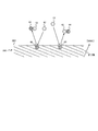
- FIG. 1 is a diagram for explaining an outline of a manufacturing method for manufacturing a SiC substrate 200 whose surface is planarized.
- FIG. 1 shows a partial cross section in the vicinity of surface 202 of SiC substrate 200.
- a SiC substrate 200 having an off angle is prepared.
- the crystal plane of the plane on which the device is to be formed is measured by a goniometer or the like, and the surface of the substrate is cut by tilting the crystal plane by a predetermined angle to prepare the SiC substrate 200 having an off angle.
- SiC substrate 200 Since the SiC substrate 200 has an off angle, the quality of the SiC thin film grown on the surface of the SiC substrate 200 can be improved.
- surface 202 of SiC substrate 200 has a predetermined off angle with respect to the (0001) plane which is a stable surface.
- the off angle is 1 ° or more and 8 ° or less.
- the off angle may be 4 ° or more and 8 ° or less.
- the surface of the SiC substrate 200 is polished and planarized by the CMP method.
- the surface 202 of the SiC substrate 200 is in a mirror state.
- Bunching is a phenomenon in which the surface of a substrate is saw-toothed with a period of about several ⁇ m and a height of about several tens of nm. This is the result of the reconstruction of the surface of the substrate to be more stable due to the presence of the off-angle. Surfaces with such large undulations can not be used for device formation.
- the SiC substrate 200 having an off angle is heated in a vacuum state.
- the surface 202 of the SiC substrate 200 is polished by a CMP method or the like.
- the heating temperature is, for example, in the range of 800 ° C. or more and 1200 ° C. or less.
- the heating temperature is lower than the temperature at which the bunching phenomenon occurs in the SiC substrate 200. More preferably, the heating temperature is 900 ° C. or more and 1100 ° C. or less.
- various methods such as a heater, electric heating, electron beam heating, infrared heating, laser heating and the like can be used.
- Atomic hydrogen is hydrogen which exists as a single atom, and is highly reactive.
- the irradiation of atomic hydrogen 42 refers to supplying atomic hydrogen 42 generated at a position away from the SiC substrate 200 to the surface 202 of the SiC substrate 200. That is, as in the technique disclosed in Non-Patent Document 1, the method of etching the surface of the SiC substrate using atomic hydrogen dissociated from hydrogen gas in the vicinity of the surface by the heat of the SiC substrate is the manufacturing method of this example. Not included in
- atomic hydrogen 42 contacts the surface 202 of the SiC substrate 200, it reacts with silicon atoms 40 on the surface 202 to become a silane-based gas. Thereby, silicon atoms 40 are detached from the surface 202 of the SiC substrate 200. Also, atomic hydrogen 42 reacts with carbon atoms 44 on the surface 202 of the SiC substrate 200 to become a hydrocarbon-based gas. Thereby, carbon atoms 44 are desorbed from the surface 202 of the SiC substrate 200.
- FIG. 2 shows the SiC substrate 200 after etching.
- the SiC substrate 200 is etched so that the terrace of the (0001) plane which is a stable surface is periodically exposed.
- the (11-2n) plane is exposed between each terrace.
- the width L of the terrace varies depending on the off angle and the off direction, but is about 10 nm to about 20 nm.
- the alternate appearance of the terraces of the (0001) plane and the (11-2n) plane forms nano-facets on the surface 204 of the SiC substrate 200.
- the nanofaceted surface 204 has the same flatness as the step-and-terrace structure of the SiC substrate 200 having no off-angle. For this reason, it can be said that it is an ideal surface in the SiC substrate 200 having an off angle.
- the shape is maintained. As the etching proceeds further, the film thickness of the SiC substrate 200 is reduced, but the shape of the nano-facets is maintained.
- the temperature of the SiC substrate 200 can be lowered, and can be set relatively freely.
- the temperature of the SiC substrate 200 can be set lower than the temperature at which bunching occurs on the surface.
- the temperature of the SiC substrate 200 may be a temperature at which the reaction of the atomic hydrogen 42 with the silicon atoms and the carbon atoms can be promoted.
- the SiC substrate 200 in the case of dissociating atomic hydrogen from hydrogen gas at the temperature of the SiC substrate 200, the SiC substrate 200 must be heated to such an extent that atomic hydrogen can be generated. As the temperature of the SiC substrate 200 is increased, the dissociation efficiency of atomic hydrogen is improved, and the etching efficiency is improved.
- the temperature of the SiC substrate 200 and the generation of atomic hydrogen can be made independent. That is, the etching efficiency and the generation of atomic hydrogen can be controlled independently. Therefore, the temperature of SiC substrate 200 can be lowered, and temperature conditions can be easily set. In addition, even if a slight deviation occurs in the off angle and the off direction, nanofacets can be stably formed with good reproducibility.
- nano-facets can be easily formed on the SiC substrate 200 with high reproducibility. Therefore, the yield of devices using the SiC substrate 200 can be improved, and the characteristics can be improved.
- FIG. 3 is a schematic view of a processing apparatus 100 for processing the SiC substrate 200. As shown in FIG. The processing apparatus 100 planarizes the surface of the SiC substrate 200 by irradiating atomic hydrogen on the surface of the SiC substrate 200.
- the processing apparatus 100 includes a processing chamber 10, a gas supply cell 20 and a hydrogen gas source 30.
- a SiC substrate 200 to be processed is introduced.
- the processing chamber 10 has a stage 12 on which the SiC substrate 200 is mounted.
- the inside of the processing chamber 10 is depressurized to a vacuum state after the SiC substrate 200 is introduced.
- the processing apparatus 100 is provided with a heating unit 14 that heats the SiC substrate 200.
- the heating unit 14 heats the SiC substrate 200 by irradiating the SiC substrate 200 with laser light through the window unit 15 provided in the processing chamber 10.
- the gas supply cell 20 is connected to the processing chamber 10.
- a connection hole 18 connecting the inside of the gas supply cell 20 and the inside of the processing chamber 10 is formed on the side wall of the processing chamber 10 in this example.
- At least one of the processing chamber 10 and the gas supply cell 20 is provided with a shutter 16 for opening and closing the connection hole 18.
- the gas supply cell 20 of this example has a tungsten filament 22.
- the hydrogen gas source 30 supplies hydrogen gas containing hydrogen molecules to the inside of the gas supply cell 20.
- hydrogen molecules are dissociatively adsorbed on the surface of the tungsten filament 22 to generate atomic hydrogen.
- the processing apparatus 100 may also generate atomic hydrogen by plasma or the like. In this case, plasma may be generated inside the processing chamber 10 to generate atomic hydrogen.
- the atomic hydrogen generated in the gas supply cell 20 is irradiated to the heated SiC substrate 200. Note that by making the inside of the processing chamber 10 in a vacuum state, atomic hydrogen can be prevented from reacting with another substance, and can be supplied to the SiC substrate 200 in the state of atomic hydrogen.
- Table 1 shows the manufacturing conditions of the respective Examples and Comparative Examples in which the surface of the SiC substrate 200 was treated, and the results of whether or not nanofacets are formed on the substrate surface.
- Each example is a sample produced by the method described in FIGS. 1 to 3.
- the amounts of materials, materials used etc., proportions of materials etc., processing details, processing procedures, orientations of elements or crystal planes etc. in each example can be suitably changed without departing from the spirit of the present invention. Accordingly, the scope of the present invention is not limited to the following examples.
- Example 1 an -n-type SiC (0001) wafer having an off angle of 4 °, an off direction of [11-20], a thickness of 430 ⁇ m, and a diameter of 3 inches was prepared. The surface of the wafer is CMP processed. An n-type epitaxial layer with a carrier concentration of 10 19 cm -3 was formed to 10 ⁇ m on the wafer by CVD.
- the wafer was diced into squares of 10 mm on a side, and then subjected to organic cleaning treatment and UVO 3 treatment at 300 ° C. for 10 minutes to form a SiC substrate.
- the SiC substrate was introduced into the processing chamber 10, and the inside of the processing chamber 10 and the gas supply cell 20 was evacuated to 2.0 ⁇ 10 ⁇ 7 Pa. Thereafter, the SiC substrate was irradiated with laser light to heat the SiC substrate. The rate of temperature rise was 20 ° C./min, and the temperature was maintained for 10 minutes after reaching 500 ° C.
- the shutter 16 was closed to heat the tungsten filament 22 of the gas supply cell 20 to 1700 ° C. While the tungsten filament 22 was heated, hydrogen gas was supplied until the degree of vacuum in the gas supply cell 20 became 1.0 ⁇ 10 ⁇ 4 Pa. The hydrogen gas is dissociatively adsorbed on the surface of the tungsten filament 22 to be atomic hydrogen. The dissociation rate is about several percent.
- the shutter 16 was opened, and atomic hydrogen was irradiated to the SiC substrate for 10 minutes.
- the irradiation amount of gas to the SiC substrate is about several ccm.
- the irradiation time and irradiation amount of atomic hydrogen can be appropriately changed.
- the irradiation time may be about 10 minutes or more and about 1 hour or less.
- the shutter 16 was closed, the temperature of the SiC substrate was lowered to room temperature, and the processing was completed.
- the treated SiC substrate was taken out to the atmosphere, and the substrate surface was observed with an atomic force microscope to confirm whether or not nanofacets were formed. As shown in Table 1, under the conditions of Example 1, nanofacets are formed.
- Example 2 produced the SiC substrate on the same conditions as Example 1 except the heating temperature of the SiC substrate having been 1200 ° C.
- the nanofacets are also formed under the conditions of Example 2.
- Example 3 produced the SiC substrate on the same conditions as Example 1 except having made the off-angle of a SiC substrate 8 degrees.
- the nanofacets are also formed under the conditions of Example 3.
- Example 4 produced the SiC substrate on the same conditions as Example 1 except having made the OFF direction of a SiC substrate into [1-100]. The nanofacets are also formed under the conditions of Example 4.
- Example 5 produced the SiC substrate on the same conditions as Example 1 except having made the polymorph of a SiC substrate into 6H. The nanofacets are also formed under the conditions of Example 5.
- Example 6 produced the SiC substrate on the same conditions as Example 1 except having made the crystal face of a SiC substrate into (000-1). The nanofacets are also formed under the conditions of Example 6.
- the comparative example 1 produced the SiC substrate on the same conditions as Example 1 except the heating temperature of the SiC substrate having been 400 degreeC. Under the conditions of Comparative Example 1, no nanofacets are formed. Under the conditions of Comparative Example 1, the surface of the SiC substrate was in the same state as before the treatment.
- the comparative example 2 produced the SiC substrate on the conditions same as Example 1 except the heating temperature of the SiC substrate having been 1300 degreeC. Under the conditions of Comparative Example 2, no nanofacets are formed. Under the conditions of Comparative Example 2, the surface of the SiC substrate was rough.
- the temperature of the SiC substrate is preferably 800 ° C. or more and 1200 ° C. or less.
- the heating temperature is not limited to this.
- the off angle of the SiC substrate may be not less than 1 degree and not more than 8 degrees.
- the off angle of the SiC substrate may be 4 degrees or more and 8 degrees or less.
- the off angle of the SiC substrate may be 4 degrees or more and 6 degrees or less. However, the off angle is not limited to this.
- the off direction of the SiC substrate may be the [11-20] or [1-100] direction. However, the off direction is not limited to this.
- the polymorph of the SiC substrate may be 4H or 6H.
- the polymorphism of the SiC substrate is not limited to this.
- the crystal plane of the SiC substrate may be (0001) or (000-1). However, the crystal plane of the SiC substrate is not limited to this.
Landscapes
- Crystals, And After-Treatments Of Crystals (AREA)
- Drying Of Semiconductors (AREA)
- Physics & Mathematics (AREA)
- Engineering & Computer Science (AREA)
- Plasma & Fusion (AREA)
- Electromagnetism (AREA)
- Optics & Photonics (AREA)
Abstract
Description
[非特許文献1]Hiroshi Nakagawa, Satoru Tanaka, and Ikuo Suemue, "Self-Ordering of Nanofacets on Vicinal SiC Surfaces"、 2003年11月26日、PHISICAL REVIEW LETTERS 91,226107.
表1に、SiC基板200の表面を処理した各実施例および各比較例の製造条件と、基板表面にナノファセットが形成されるか否かの結果を示す。各実施例は、図1から図3において説明した方法で作製したサンプルである。各実施例における材料、材料等の使用量、材料等の割合、処理内容、処理手順、要素または結晶面等の向き等は、本発明の趣旨を逸脱しない範囲で、適宜変更することができる。従って、本発明の範囲は以下の実施例に限定されない。

Claims (7)
- 表面を平坦化したSiC基板を製造する製造方法であって、
オフ角を有するSiC基板を加熱した状態で、前記SiC基板の表面に原子状水素を照射して、前記SiC基板の表面をエッチングする段階を備える製造方法。 - 前記エッチングする段階において、前記SiC基板を800℃以上且つ1200℃以下の範囲で加熱する
請求項1に記載の製造方法。 - 前記SiC基板のオフ角が、1°以上且つ8°以下である
請求項1または2に記載の製造方法。 - 前記SiC基板のオフ方向が、[11-20]または[1-100]方向である
請求項1から3のいずれか一項に記載の製造方法。 - 前記SiC基板の多形が4Hまたは6Hである
請求項1から4のいずれか一項に記載の製造方法。 - 前記SiC基板の前記表面の結晶面が(0001)または(000-1)である
請求項1から5のいずれか一項に記載の製造方法。 - 前記SiC基板が載置された処理室に連結されたガス供給セルにおいて、水素を含む原料ガスから前記原子状水素を生成する段階を更に備える
請求項1から6のいずれか一項に記載の製造方法。
Priority Applications (5)
| Application Number | Priority Date | Filing Date | Title |
|---|---|---|---|
| DE112015006240.8T DE112015006240T5 (de) | 2015-07-30 | 2015-07-30 | HERSTELLUNGSVERFAHREN EINES SiC-SUBSTRATS |
| CN201580078145.6A CN107431005B (zh) | 2015-07-30 | 2015-07-30 | SiC基板的制造方法 |
| JP2017530979A JP6447732B2 (ja) | 2015-07-30 | 2015-07-30 | SiC基板の製造方法 |
| PCT/JP2015/071723 WO2017017858A1 (ja) | 2015-07-30 | 2015-07-30 | SiC基板の製造方法 |
| US15/709,411 US10297450B2 (en) | 2015-07-30 | 2017-09-19 | Manufacturing method of SiC substrate |
Applications Claiming Priority (1)
| Application Number | Priority Date | Filing Date | Title |
|---|---|---|---|
| PCT/JP2015/071723 WO2017017858A1 (ja) | 2015-07-30 | 2015-07-30 | SiC基板の製造方法 |
Related Child Applications (1)
| Application Number | Title | Priority Date | Filing Date |
|---|---|---|---|
| US15/709,411 Continuation US10297450B2 (en) | 2015-07-30 | 2017-09-19 | Manufacturing method of SiC substrate |
Publications (1)
| Publication Number | Publication Date |
|---|---|
| WO2017017858A1 true WO2017017858A1 (ja) | 2017-02-02 |
Family
ID=57884211
Family Applications (1)
| Application Number | Title | Priority Date | Filing Date |
|---|---|---|---|
| PCT/JP2015/071723 Ceased WO2017017858A1 (ja) | 2015-07-30 | 2015-07-30 | SiC基板の製造方法 |
Country Status (5)
| Country | Link |
|---|---|
| US (1) | US10297450B2 (ja) |
| JP (1) | JP6447732B2 (ja) |
| CN (1) | CN107431005B (ja) |
| DE (1) | DE112015006240T5 (ja) |
| WO (1) | WO2017017858A1 (ja) |
Cited By (1)
| Publication number | Priority date | Publication date | Assignee | Title |
|---|---|---|---|---|
| JP2024129916A (ja) * | 2023-03-14 | 2024-09-30 | 株式会社東芝 | 半導体装置の製造方法 |
Families Citing this family (1)
| Publication number | Priority date | Publication date | Assignee | Title |
|---|---|---|---|---|
| WO2022130788A1 (ja) * | 2020-12-18 | 2022-06-23 | 国立大学法人京都大学 | SiC半導体素子の製造方法及びSiCMOSFET |
Citations (2)
| Publication number | Priority date | Publication date | Assignee | Title |
|---|---|---|---|---|
| JP2003234301A (ja) * | 2001-10-25 | 2003-08-22 | Matsushita Electric Ind Co Ltd | 半導体基板、半導体素子及びその製造方法 |
| JP2005317670A (ja) * | 2004-04-27 | 2005-11-10 | Japan Science & Technology Agency | (100)配向した立方晶炭化珪素結晶膜の作製方法 |
Family Cites Families (8)
| Publication number | Priority date | Publication date | Assignee | Title |
|---|---|---|---|---|
| JP2001332508A (ja) * | 2000-05-23 | 2001-11-30 | Matsushita Electric Ind Co Ltd | 半導体素子の製造方法 |
| EP1306890A2 (en) * | 2001-10-25 | 2003-05-02 | Matsushita Electric Industrial Co., Ltd. | Semiconductor substrate and device comprising SiC and method for fabricating the same |
| JP2008205296A (ja) * | 2007-02-21 | 2008-09-04 | Matsushita Electric Ind Co Ltd | 炭化珪素半導体素子及びその製造方法 |
| JP4887418B2 (ja) * | 2009-12-14 | 2012-02-29 | 昭和電工株式会社 | SiCエピタキシャルウェハの製造方法 |
| US8927396B2 (en) | 2010-11-17 | 2015-01-06 | Nippon Steel & Sumitomo Metal Corporation | Production process of epitaxial silicon carbide single crystal substrate |
| CN102534808B (zh) * | 2010-12-14 | 2014-11-05 | 北京天科合达蓝光半导体有限公司 | 高质量碳化硅表面的获得方法 |
| JP5786759B2 (ja) * | 2012-02-21 | 2015-09-30 | 新日鐵住金株式会社 | エピタキシャル炭化珪素ウエハの製造方法 |
| JP6112712B2 (ja) * | 2013-03-27 | 2017-04-12 | 国立研究開発法人産業技術総合研究所 | 炭化珪素エピタキシャルウエハの製造方法 |
-
2015
- 2015-07-30 DE DE112015006240.8T patent/DE112015006240T5/de active Granted
- 2015-07-30 JP JP2017530979A patent/JP6447732B2/ja active Active
- 2015-07-30 CN CN201580078145.6A patent/CN107431005B/zh active Active
- 2015-07-30 WO PCT/JP2015/071723 patent/WO2017017858A1/ja not_active Ceased
-
2017
- 2017-09-19 US US15/709,411 patent/US10297450B2/en active Active
Patent Citations (2)
| Publication number | Priority date | Publication date | Assignee | Title |
|---|---|---|---|---|
| JP2003234301A (ja) * | 2001-10-25 | 2003-08-22 | Matsushita Electric Ind Co Ltd | 半導体基板、半導体素子及びその製造方法 |
| JP2005317670A (ja) * | 2004-04-27 | 2005-11-10 | Japan Science & Technology Agency | (100)配向した立方晶炭化珪素結晶膜の作製方法 |
Cited By (2)
| Publication number | Priority date | Publication date | Assignee | Title |
|---|---|---|---|---|
| JP2024129916A (ja) * | 2023-03-14 | 2024-09-30 | 株式会社東芝 | 半導体装置の製造方法 |
| JP7771117B2 (ja) | 2023-03-14 | 2025-11-17 | 株式会社東芝 | 半導体装置の製造方法 |
Also Published As
| Publication number | Publication date |
|---|---|
| US20180005828A1 (en) | 2018-01-04 |
| CN107431005B (zh) | 2020-11-13 |
| US10297450B2 (en) | 2019-05-21 |
| DE112015006240T5 (de) | 2017-11-09 |
| JPWO2017017858A1 (ja) | 2018-01-18 |
| CN107431005A (zh) | 2017-12-01 |
| JP6447732B2 (ja) | 2019-01-09 |
Similar Documents
| Publication | Publication Date | Title |
|---|---|---|
| CN101798706B (zh) | 在碳化硅(SiC)基底上外延生长石墨烯的方法 | |
| US9379000B2 (en) | Method for producing nanocarbon film and nanocarbon film | |
| CN101652835B (zh) | 具有碳化硅基板的半导体器件的退火方法和半导体器件 | |
| CN103614779B (zh) | 一种提高碳化硅外延片片内n型掺杂浓度均匀性的方法 | |
| JP5316612B2 (ja) | 炭化珪素半導体エピタキシャル基板の製造方法 | |
| US20110315074A1 (en) | Single-crystal diamond growth base material and method for manufacturing single-crystal diamond substrate | |
| CN105441902B (zh) | 一种外延碳化硅‑石墨烯复合薄膜的制备方法 | |
| WO2011158528A1 (ja) | 炭化珪素半導体装置の製造方法および炭化珪素半導体装置の製造装置 | |
| JP2006032655A (ja) | 炭化珪素基板の製造方法 | |
| JP2009149481A (ja) | 半導体基板の製造方法 | |
| JP2008053343A (ja) | 炭化珪素半導体エピタキシャル基板の製造方法 | |
| CN114242644B (zh) | 一种碳化硅沟槽结构外延填充方法 | |
| CN106169497B (zh) | 碳化硅基板以及碳化硅基板的制造方法 | |
| JP2017041503A (ja) | 半導体装置、および、その製造方法 | |
| JP6447732B2 (ja) | SiC基板の製造方法 | |
| CN107316804A (zh) | 一种金属原子掺杂的大面积规则外延石墨烯的制备方法 | |
| JP6927429B2 (ja) | SiCエピタキシャル基板の製造方法 | |
| JP5168990B2 (ja) | 半導体基板の製造方法 | |
| TWI719085B (zh) | 用以清潔砷化銦鎵(或三五族)基板的方法及解決方案 | |
| WO2020230602A1 (ja) | ダイヤモンド結晶基板及びダイヤモンド結晶基板の製造方法 | |
| WO2025055183A1 (zh) | 一种掺杂金刚石制备方法 | |
| KR20240119289A (ko) | 다이아몬드 막 증착을 위한 기상 전구체 시딩 | |
| CN108046246A (zh) | 一种工艺气体辅助的石墨烯薄膜生长方法 | |
| JP2010153272A (ja) | イオン注入方法、及び炭化シリコンの製造方法 | |
| JP4690734B2 (ja) | 単結晶SiC基板の製造方法 |
Legal Events
| Date | Code | Title | Description |
|---|---|---|---|
| 121 | Ep: the epo has been informed by wipo that ep was designated in this application |
Ref document number: 15899691 Country of ref document: EP Kind code of ref document: A1 |
|
| ENP | Entry into the national phase |
Ref document number: 2017530979 Country of ref document: JP Kind code of ref document: A |
|
| WWE | Wipo information: entry into national phase |
Ref document number: 112015006240 Country of ref document: DE |
|
| 122 | Ep: pct application non-entry in european phase |
Ref document number: 15899691 Country of ref document: EP Kind code of ref document: A1 |