WO2017010063A1 - 配線基板及びその製造方法 - Google Patents
配線基板及びその製造方法 Download PDFInfo
- Publication number
- WO2017010063A1 WO2017010063A1 PCT/JP2016/003218 JP2016003218W WO2017010063A1 WO 2017010063 A1 WO2017010063 A1 WO 2017010063A1 JP 2016003218 W JP2016003218 W JP 2016003218W WO 2017010063 A1 WO2017010063 A1 WO 2017010063A1
- Authority
- WO
- WIPO (PCT)
- Prior art keywords
- layer
- resin layer
- opening
- metal layer
- base material
- Prior art date
- Legal status (The legal status is an assumption and is not a legal conclusion. Google has not performed a legal analysis and makes no representation as to the accuracy of the status listed.)
- Ceased
Links
Images


Classifications
-
- H—ELECTRICITY
- H05—ELECTRIC TECHNIQUES NOT OTHERWISE PROVIDED FOR
- H05K—PRINTED CIRCUITS; CASINGS OR CONSTRUCTIONAL DETAILS OF ELECTRIC APPARATUS; MANUFACTURE OF ASSEMBLAGES OF ELECTRICAL COMPONENTS
- H05K1/00—Printed circuits
- H05K1/02—Details
- H05K1/0271—Arrangements for reducing stress or warp in rigid printed circuit boards, e.g. caused by loads, vibrations or differences in thermal expansion
-
- H—ELECTRICITY
- H10—SEMICONDUCTOR DEVICES; ELECTRIC SOLID-STATE DEVICES NOT OTHERWISE PROVIDED FOR
- H10W—GENERIC PACKAGES, INTERCONNECTIONS, CONNECTORS OR OTHER CONSTRUCTIONAL DETAILS OF DEVICES COVERED BY CLASS H10
- H10W70/00—Package substrates; Interposers; Redistribution layers [RDL]
- H10W70/60—Insulating or insulated package substrates; Interposers; Redistribution layers
- H10W70/67—Insulating or insulated package substrates; Interposers; Redistribution layers characterised by their insulating layers or insulating parts
- H10W70/69—Insulating materials thereof
- H10W70/692—Ceramics or glasses
-
- H—ELECTRICITY
- H05—ELECTRIC TECHNIQUES NOT OTHERWISE PROVIDED FOR
- H05K—PRINTED CIRCUITS; CASINGS OR CONSTRUCTIONAL DETAILS OF ELECTRIC APPARATUS; MANUFACTURE OF ASSEMBLAGES OF ELECTRICAL COMPONENTS
- H05K1/00—Printed circuits
- H05K1/02—Details
- H05K1/0274—Optical details, e.g. printed circuits comprising integral optical means
-
- H—ELECTRICITY
- H05—ELECTRIC TECHNIQUES NOT OTHERWISE PROVIDED FOR
- H05K—PRINTED CIRCUITS; CASINGS OR CONSTRUCTIONAL DETAILS OF ELECTRIC APPARATUS; MANUFACTURE OF ASSEMBLAGES OF ELECTRICAL COMPONENTS
- H05K3/00—Apparatus or processes for manufacturing printed circuits
- H05K3/02—Apparatus or processes for manufacturing printed circuits in which the conductive material is applied to the surface of the insulating support and is thereafter removed from such areas of the surface which are not intended for current conducting or shielding
-
- H—ELECTRICITY
- H10—SEMICONDUCTOR DEVICES; ELECTRIC SOLID-STATE DEVICES NOT OTHERWISE PROVIDED FOR
- H10W—GENERIC PACKAGES, INTERCONNECTIONS, CONNECTORS OR OTHER CONSTRUCTIONAL DETAILS OF DEVICES COVERED BY CLASS H10
- H10W70/00—Package substrates; Interposers; Redistribution layers [RDL]
- H10W70/60—Insulating or insulated package substrates; Interposers; Redistribution layers
- H10W70/67—Insulating or insulated package substrates; Interposers; Redistribution layers characterised by their insulating layers or insulating parts
- H10W70/68—Shapes or dispositions thereof
-
- H—ELECTRICITY
- H05—ELECTRIC TECHNIQUES NOT OTHERWISE PROVIDED FOR
- H05K—PRINTED CIRCUITS; CASINGS OR CONSTRUCTIONAL DETAILS OF ELECTRIC APPARATUS; MANUFACTURE OF ASSEMBLAGES OF ELECTRICAL COMPONENTS
- H05K1/00—Printed circuits
- H05K1/02—Details
- H05K1/03—Use of materials for the substrate
- H05K1/0306—Inorganic insulating substrates, e.g. ceramic, glass
-
- H—ELECTRICITY
- H05—ELECTRIC TECHNIQUES NOT OTHERWISE PROVIDED FOR
- H05K—PRINTED CIRCUITS; CASINGS OR CONSTRUCTIONAL DETAILS OF ELECTRIC APPARATUS; MANUFACTURE OF ASSEMBLAGES OF ELECTRICAL COMPONENTS
- H05K2201/00—Indexing scheme relating to printed circuits covered by H05K1/00
- H05K2201/01—Dielectrics
- H05K2201/0104—Properties and characteristics in general
- H05K2201/0108—Transparent
-
- H—ELECTRICITY
- H05—ELECTRIC TECHNIQUES NOT OTHERWISE PROVIDED FOR
- H05K—PRINTED CIRCUITS; CASINGS OR CONSTRUCTIONAL DETAILS OF ELECTRIC APPARATUS; MANUFACTURE OF ASSEMBLAGES OF ELECTRICAL COMPONENTS
- H05K2201/00—Indexing scheme relating to printed circuits covered by H05K1/00
- H05K2201/10—Details of components or other objects attached to or integrated in a printed circuit board
- H05K2201/10007—Types of components
- H05K2201/10121—Optical component, e.g. opto-electronic component
-
- H—ELECTRICITY
- H10—SEMICONDUCTOR DEVICES; ELECTRIC SOLID-STATE DEVICES NOT OTHERWISE PROVIDED FOR
- H10F—INORGANIC SEMICONDUCTOR DEVICES SENSITIVE TO INFRARED RADIATION, LIGHT, ELECTROMAGNETIC RADIATION OF SHORTER WAVELENGTH OR CORPUSCULAR RADIATION
- H10F39/00—Integrated devices, or assemblies of multiple devices, comprising at least one element covered by group H10F30/00, e.g. radiation detectors comprising photodiode arrays
- H10F39/80—Constructional details of image sensors
- H10F39/804—Containers or encapsulations
-
- H—ELECTRICITY
- H10—SEMICONDUCTOR DEVICES; ELECTRIC SOLID-STATE DEVICES NOT OTHERWISE PROVIDED FOR
- H10W—GENERIC PACKAGES, INTERCONNECTIONS, CONNECTORS OR OTHER CONSTRUCTIONAL DETAILS OF DEVICES COVERED BY CLASS H10
- H10W42/00—Arrangements for protection of devices
- H10W42/121—Arrangements for protection of devices protecting against mechanical damage
-
- H—ELECTRICITY
- H10—SEMICONDUCTOR DEVICES; ELECTRIC SOLID-STATE DEVICES NOT OTHERWISE PROVIDED FOR
- H10W—GENERIC PACKAGES, INTERCONNECTIONS, CONNECTORS OR OTHER CONSTRUCTIONAL DETAILS OF DEVICES COVERED BY CLASS H10
- H10W70/00—Package substrates; Interposers; Redistribution layers [RDL]
- H10W70/01—Manufacture or treatment
- H10W70/05—Manufacture or treatment of insulating or insulated package substrates, or of interposers, or of redistribution layers
-
- H—ELECTRICITY
- H10—SEMICONDUCTOR DEVICES; ELECTRIC SOLID-STATE DEVICES NOT OTHERWISE PROVIDED FOR
- H10W—GENERIC PACKAGES, INTERCONNECTIONS, CONNECTORS OR OTHER CONSTRUCTIONAL DETAILS OF DEVICES COVERED BY CLASS H10
- H10W70/00—Package substrates; Interposers; Redistribution layers [RDL]
- H10W70/60—Insulating or insulated package substrates; Interposers; Redistribution layers
- H10W70/67—Insulating or insulated package substrates; Interposers; Redistribution layers characterised by their insulating layers or insulating parts
- H10W70/68—Shapes or dispositions thereof
- H10W70/685—Shapes or dispositions thereof comprising multiple insulating layers
-
- H—ELECTRICITY
- H10—SEMICONDUCTOR DEVICES; ELECTRIC SOLID-STATE DEVICES NOT OTHERWISE PROVIDED FOR
- H10W—GENERIC PACKAGES, INTERCONNECTIONS, CONNECTORS OR OTHER CONSTRUCTIONAL DETAILS OF DEVICES COVERED BY CLASS H10
- H10W72/00—Interconnections or connectors in packages
- H10W72/071—Connecting or disconnecting
- H10W72/072—Connecting or disconnecting of bump connectors
-
- H—ELECTRICITY
- H10—SEMICONDUCTOR DEVICES; ELECTRIC SOLID-STATE DEVICES NOT OTHERWISE PROVIDED FOR
- H10W—GENERIC PACKAGES, INTERCONNECTIONS, CONNECTORS OR OTHER CONSTRUCTIONAL DETAILS OF DEVICES COVERED BY CLASS H10
- H10W72/00—Interconnections or connectors in packages
- H10W72/071—Connecting or disconnecting
- H10W72/073—Connecting or disconnecting of die-attach connectors
-
- H—ELECTRICITY
- H10—SEMICONDUCTOR DEVICES; ELECTRIC SOLID-STATE DEVICES NOT OTHERWISE PROVIDED FOR
- H10W—GENERIC PACKAGES, INTERCONNECTIONS, CONNECTORS OR OTHER CONSTRUCTIONAL DETAILS OF DEVICES COVERED BY CLASS H10
- H10W72/00—Interconnections or connectors in packages
- H10W72/20—Bump connectors, e.g. solder bumps or copper pillars; Dummy bumps; Thermal bumps
- H10W72/251—Materials
- H10W72/252—Materials comprising solid metals or solid metalloids, e.g. PbSn, Ag or Cu
-
- H—ELECTRICITY
- H10—SEMICONDUCTOR DEVICES; ELECTRIC SOLID-STATE DEVICES NOT OTHERWISE PROVIDED FOR
- H10W—GENERIC PACKAGES, INTERCONNECTIONS, CONNECTORS OR OTHER CONSTRUCTIONAL DETAILS OF DEVICES COVERED BY CLASS H10
- H10W72/00—Interconnections or connectors in packages
- H10W72/30—Die-attach connectors
- H10W72/351—Materials of die-attach connectors
- H10W72/353—Materials of die-attach connectors not comprising solid metals or solid metalloids, e.g. ceramics
- H10W72/354—Materials of die-attach connectors not comprising solid metals or solid metalloids, e.g. ceramics comprising polymers
-
- H—ELECTRICITY
- H10—SEMICONDUCTOR DEVICES; ELECTRIC SOLID-STATE DEVICES NOT OTHERWISE PROVIDED FOR
- H10W—GENERIC PACKAGES, INTERCONNECTIONS, CONNECTORS OR OTHER CONSTRUCTIONAL DETAILS OF DEVICES COVERED BY CLASS H10
- H10W72/00—Interconnections or connectors in packages
- H10W72/851—Dispositions of multiple connectors or interconnections
- H10W72/853—On the same surface
- H10W72/856—Bump connectors and die-attach connectors
-
- H—ELECTRICITY
- H10—SEMICONDUCTOR DEVICES; ELECTRIC SOLID-STATE DEVICES NOT OTHERWISE PROVIDED FOR
- H10W—GENERIC PACKAGES, INTERCONNECTIONS, CONNECTORS OR OTHER CONSTRUCTIONAL DETAILS OF DEVICES COVERED BY CLASS H10
- H10W90/00—Package configurations
- H10W90/701—Package configurations characterised by the relative positions of pads or connectors relative to package parts
-
- H—ELECTRICITY
- H10—SEMICONDUCTOR DEVICES; ELECTRIC SOLID-STATE DEVICES NOT OTHERWISE PROVIDED FOR
- H10W—GENERIC PACKAGES, INTERCONNECTIONS, CONNECTORS OR OTHER CONSTRUCTIONAL DETAILS OF DEVICES COVERED BY CLASS H10
- H10W90/00—Package configurations
- H10W90/701—Package configurations characterised by the relative positions of pads or connectors relative to package parts
- H10W90/721—Package configurations characterised by the relative positions of pads or connectors relative to package parts of bump connectors
- H10W90/724—Package configurations characterised by the relative positions of pads or connectors relative to package parts of bump connectors between a chip and a stacked insulating package substrate, interposer or RDL
-
- H—ELECTRICITY
- H10—SEMICONDUCTOR DEVICES; ELECTRIC SOLID-STATE DEVICES NOT OTHERWISE PROVIDED FOR
- H10W—GENERIC PACKAGES, INTERCONNECTIONS, CONNECTORS OR OTHER CONSTRUCTIONAL DETAILS OF DEVICES COVERED BY CLASS H10
- H10W90/00—Package configurations
- H10W90/701—Package configurations characterised by the relative positions of pads or connectors relative to package parts
- H10W90/731—Package configurations characterised by the relative positions of pads or connectors relative to package parts of die-attach connectors
- H10W90/734—Package configurations characterised by the relative positions of pads or connectors relative to package parts of die-attach connectors between a chip and a stacked insulating package substrate, interposer or RDL
Definitions
- the present invention relates to a wiring board and a manufacturing method thereof.
- the present invention includes a light-transmitting base material, a laminate formed by laminating a metal layer and a resin layer on at least one side of the base material, and a light transmission portion that is an opening provided in a part of the laminate. And at least part of the side surface defining the light transmission part is made of a resin layer, adjacent to the resin layer constituting at least part of the side surface defining the light transmission part in the vicinity of the surface of the base material, and A part of the metal layer is disposed so as to surround the resin layer.
- the present invention also provides a light-transmitting base material, a laminate formed by laminating a metal layer and a resin layer on at least one side of the base material, and an optical transmission that is an opening provided in a part of the laminate. And a part of the metal layer is disposed so as to surround the light transmission part in the vicinity of the surface of the base material.
- the present invention also includes a step of forming a metal layer so as to cover a region where the light transmitting part is formed on the light-transmitting substrate and the periphery thereof, and a step of forming a resin layer so as to cover the formed metal layer And a step of selectively removing a part of the resin layer on the formation region of the light transmission portion to form the opening, and a step of removing the metal layer exposed from the opening. It is a manufacturing method of a wiring board.
- the wiring board and the manufacturing method thereof of the present invention capable of suppressing the generation of cracks in the base material when forming the light transmitting portion, having high light transmittance, and capable of forming a fine wiring, and its Manufacturing can be realized.
- FIG. 1 is a diagram for explaining a semiconductor device manufactured using the wiring board of this embodiment.
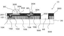
- FIG. 2 is a diagram illustrating the wiring board according to the present embodiment.
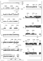
- FIG. 3 is a view for explaining another wiring board according to the present embodiment.
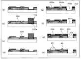
- FIG. 4 is a diagram for explaining the manufacturing process of the wiring board according to the present embodiment in (a) to (o).
- FIG. 5A to FIG. 5H are views for explaining another wiring board manufacturing process according to the present embodiment from (a) to (h).
- FIG. 1 is a diagram illustrating a semiconductor device manufactured using the wiring board of the present embodiment.
- the semiconductor device 1 includes a stacked body 101, a stacked body 201, a light transmission unit 60, a base material 30, a joining terminal 80, an external connection terminal 90, a component 70, a sealing member. And a stop resin 100.
- the details of the stacked body 101, the stacked body 201, and the light transmission unit 60 will be described later.
- the component 70 is, for example, an integrated circuit (IC or LSI) having a transistor or a diode formed on the surface of a semiconductor substrate, and has a substantially rectangular parallelepiped shape.
- the semiconductor substrate for example, a substrate mainly composed of an inorganic substance such as a silicon substrate (Si substrate), a gallium nitride substrate (GaN substrate), or a silicon carbide substrate (SiC substrate) is used.
- a silicon substrate is used as the semiconductor substrate.
- the linear expansion coefficient (CTE: Coefficient of Thermal Expansion) of the component 70 formed using the silicon substrate is about 2 to 4 ppm / K (for example, 3 ppm / K).
- the linear expansion coefficient in the present embodiment is a length that changes in response to a temperature rise within a temperature range of 20 ° C. or more and 260 ° C. or less, for example.
- the component 70 may be a solid-state image sensor such as a CMOS sensor or a CCD sensor.
- the base material 30 is made of a material having a property of transmitting light (transparency), for example.
- the thickness of the base material 30 is 0.05 mm or more and 1 mm or less, for example.
- the main surface 30a of the substrate 30 has, for example, a substantially rectangular shape, a substantially circular shape, or a substantially elliptical shape.
- the range of the wavelength of light transmitted through the base material 30 may be, for example, 100 nm or more and 20000 nm or less, or 300 nm or more and 1100 nm or less.
- glass is used for the base material 30, for example. When glass is used, the component type and component ratio in the glass and the production method thereof are not limited.
- examples of the glass include alkali-free glass, alkali glass, borosilicate glass, quartz glass, sapphire glass, and photosensitive glass, and any glass may be used.
- examples of the manufacturing method include a float method, a downdraw method, a fusion method, an updraw method, a rollout method, and the like. Glass produced by any method may be used.
- the linear expansion coefficient of the glass is preferably close to the linear expansion coefficient of the component 70 described above, for example, -1 ppm / K or more and 10.0 ppm / K or less, or 0.5 ppm / K or more and 5.0 ppm / K or less. It is.
- the maximum height roughness Rz on the main surface 30a of the base material 30 based on JIS B 0601: 2013 may be, for example, 0.01 ⁇ m or more and 5 ⁇ m or less, or 0.1 ⁇ m or more and 3 ⁇ m or less.
- the maximum height roughness Rz of the main surface 30a of the base material 30 is 0.01 ⁇ m or more, an increase in cost for preparing the base material 30 can be suppressed.
- the maximum height roughness Rz of the main surface 30a of the base material 30 is 5 ⁇ m or less, the conductor layer can be prevented from being disconnected or short-circuited due to the irregularities of the main surface 30a, and high-density mounting can be achieved by miniaturizing the wiring. Is possible.
- the junction terminal 80 and the external connection terminal 90 are both provided on the laminate 201, and the junction terminal 80 is electrically connected to the component 70.
- the junction terminal 80 and the external connection terminal 90 are formed of solder such as Sn, Sn—Pb, Sn—Ag, Sn—Cu, Sn—Ag—Cu, or Sn—Bi.
- solder such as Sn, Sn—Pb, Sn—Ag, Sn—Cu, Sn—Ag—Cu, or Sn—Bi.
- Ni plating is applied to a portion where the metal layer is exposed on the main surface 201a of the stacked body 201.
- Au plating, Sn plating, pre-solder treatment, or organic film treatment such as OSP (Organic Solderability Preservative) may be performed.
- the wiring board 11 according to this embodiment and the other wiring board 12 according to this embodiment include a base material 30, a laminated body 101, a laminated body 201, and The light transmission part 60, the junction terminal 80, the external connection terminal 90, and the metal layer 500 are provided.
- the stacked body 101 includes a seed layer 102, a metal layer 103, a part of the metal layer 202, a part of the seed layer 106, a part of the via 104, and a resin layer 105.
- the stacked body 201 includes a part of the metal layer 202, a part of the seed layer 106, a part of the via 104, a resin layer 203, and a surface treatment layer 204.
- vias may be formed in the base material 30 and metal may be formed in the vias.
- the number of laminations can be increased by increasing the number of laminates composed of resin layers and metal layers.
- the surface treatment layer 204 is made of a single layer or a composite layer having a thickness of 0.001 ⁇ m to 3 ⁇ m, for example.
- Au, Pd, Sn, Cu, Ni can be applied in a single layer, and Au / Ni, Au / Pd, Au / Pd / Ni can be applied in a composite layer.
- the metal layer can be formed by a plating method typified by a wet process or a sputtering method typified by a vacuum process. However, it is desirable to use a plating method in terms of tact, and electroless plating, electrolytic Any method of plating may be used.
- the Ni plating film may contain inorganic substances such as phosphorus and boron, and the Pd film contains W other than the above inorganic substances.
- the surface treatment layer 204 may be provided with an organic film such as OSP.
- the seed layer 102 and the seed layer 106 are, for example, Cu, Al, Ti, Cr, Mo, W, Ta, Au, Ir, Ru, Pd, Pt, AlSi, AlSiCu, AlCu, NiFe, ITO, IZO, AZO, ZnO. , PZT, TiN, Cu 3 N 4 or the like can be applied alone or in combination, and the thickness is, for example, 0.0001 ⁇ m or more and 10 ⁇ m or less.
- the metal layer 103 and the metal layer 202 are conductive layers made of metal such as Au, Cu, and Ni, and are provided in the resin layer 105 and the resin layer 203.
- the metal layer 202 is electrically connected to the seed layer 102 and the metal layer 103 through the via 104 in the stacked body 101.
- the thickness of the metal layer 103 and the metal layer 202 is, for example, not less than 1 ⁇ m and not more than 20 ⁇ m. Note that a metal paste which is a composite material of a metal and an organic material may be applied to part of the metal layer 202.
- the metal layer 500 includes a part of the seed layer 102 and a part of the metal layer 103, and is a part that is not removed by etching when the light transmission part 60 is formed.
- the thickness of the metal layer 500 is, for example, 1.0001 ⁇ m or more and 30 ⁇ m or less.
- the resin layer 105 and the resin layer 203 include, for example, a resin material such as epoxy resin, polyimide, maleimide resin, polyethylene terephthalate, polyphenylene oxide, liquid crystal polymer, antireflection layer, infrared cut layer, or silicone, and a composite material thereof.
- the resin layer 105 of the wiring board 11 and the wiring board 12 may use either a photosensitive material or a non-photosensitive material.
- a photosensitive material is used for the resin layer 203 of the wiring substrate 11. Either a photosensitive material or a non-photosensitive material may be used for the resin layer 203 of the wiring board 12.
- the thickness of the resin layer 105 is, for example, 5 ⁇ m or more and 50 ⁇ m or less.
- the thickness of the resin layer 203 is, for example, 5 ⁇ m or more and 50 ⁇ m or less.
- the opening 205 and the opening 206 of the resin layer 203 may have the same shape and size, and the opening 205 may be larger than the opening 206 and the opening 205 may be smaller than the opening 206.
- the surface treatment layer 204 is formed on the light transmission part side of the metal layer 500.
- a seed layer 102 is applied to one side of the substrate 30.
- the seed layer 102 is formed by, for example, a known sputtering method, CVD method, or electroless plating method.
- it is formed by a Cu layer, a Cu layer plated with Ni, a Cu layer plated with Au, a Cu layer plated with solder, an Al layer, an Ag / Pd alloy layer, or the like.
- a Cu layer is used from the viewpoints of cost, electrical characteristics, and manufacturability.
- a resin layer 300 is formed on the seed layer 102.
- the resin layer 300 is formed by a known method such as a printing method, a vacuum press method, a vacuum laminating method, a roll laminating method, a spin coating method, a die coating method, a curtain coating method, or a roller coating method.
- the openings 300a and 300b are formed by removing a part of the resin layer by performing laser irradiation or photolithography on the resin layer 300.
- the opening part 300a is a part which becomes a light transmission part.
- a photosensitive resin that can be formed by photolithography is used from the viewpoints of cost, electrical characteristics, and manufacturability.
- a metal layer 103 is formed in the openings 300a and 300b.
- the metal layer 103 is formed by a printing method, an electroless plating method, or an electrolytic plating method, but in this embodiment, an electrolytic plating method is used from the viewpoint of cost, electrical characteristics, and manufacturability, and the metal layer 103 is formed on the metal layer 103.
- Cu layer is used.
- the seed layer 102a where the metal layer 103 is not formed is removed, and as shown in FIG. 4E, the metal layer 103a is removed. , 103b, 103c are obtained.
- the seed layer 102a is removed by wet etching or dry etching, for example. That is, the wiring pattern in this embodiment is formed by a semi-additive method. In the semi-additive method, a seed layer such as a Cu layer is formed, a resist having a desired pattern is formed on the seed layer, and an exposed portion of the seed layer is thickened by an electrolytic plating method or the like to remove the resist. Thereafter, a thin seed layer is etched to obtain a wiring pattern.
- a resin layer 105 is formed so as to cover the base material 30 and the metal layers 103a, 103b, and 103c.
- the resin layer 105 is formed by a known method such as a printing method, a vacuum press method, a vacuum laminating method, a roll laminating method, a spin coating method, a die coating method, a curtain coating method, or a roller coating method.
- a vacuum laminating method and a vacuum pressing method are used from the viewpoint of ease of manufacture.
- an opening 105a is provided in the resin layer 105 on the metal layer 103a, and an opening 105b is provided in the resin layer 105 on the metal layers 103b and 103c.
- the opening 105a and the opening 105b are formed by photolithography or laser when the resin layer 105 is photosensitive, and are formed by laser when the resin layer 105 is non-photosensitive.
- ⁇ 105a which is the diameter of the opening 105a needs to be smaller than ⁇ 103a which is the diameter of the metal layer 103a. Thereby, damage to the base material 30 can be suppressed, and generation of cracks when glass is used for the base material 30 can be avoided. This point will be described later.
- the metal layer 103a has an effect of releasing the heat of the laser, and if the metal layer 103a is not provided and the base material 30 is made of glass, there is a possibility that cracks may occur.
- the resin layer 400 is provided so as to protect the opening 105b, and the opening 400a is formed.
- the opening 400a is formed by photolithography or laser when the resin layer 400 is photosensitive, and is formed by laser when the resin layer 400 is non-photosensitive.
- a photosensitive resin that can be formed by photolithography is used from the viewpoints of cost, electrical characteristics, and manufacturability.
- the metal layer 103a and the seed layer 102 in the opening 400a are removed to form the light transmission part 60.
- the metal layer 103a and the seed layer 102 are removed by wet etching or dry etching, but wet etching is applied from the viewpoints of cost and manufacturability.
- the metal layer 500 is formed on the outer periphery of the light transmission portion 60 by the metal layer 103a and the seed layer 102 remaining by etching.
- the resin layer 400 is peeled off. For example, the resin layer is peeled off and removed in an alkaline solution.
- the seed layer 106 is formed by, for example, a known sputtering method, CVD method, or electroless plating method. For example, it is formed by a Cu layer, a Cu layer plated with Ni, a Cu layer plated with Au, a Cu layer plated with solder, an Al layer, an Ag / Pd alloy layer, or the like. In the present embodiment, a Cu layer is used from the viewpoints of cost, electrical characteristics, and manufacturability.
- the resin layer 107 is formed on the seed layer 106 by the same processing as the processing of the resin layer 400, and the opening 107a and the opening 107b are provided.
- a metal layer 202 is formed in the opening 107a and the opening 107b.
- the resin layer 107 is peeled and removed in, for example, an alkaline solution, and then the unnecessary seed layer 106 is removed by etching to obtain a wiring substrate shown in FIG.
- an opening 203a, an opening 203b, and an opening 203c are provided.
- a photosensitive resin is used for the resin layer 203, and the opening 203a, the opening 203b, and the opening 203c are formed by photolithography.
- the resin layer 203 constituting the inner wall of the opening 203c is in contact with the inner periphery of the metal layer 500.
- the surface treatment layer 204 is provided on the metal layer 202 in the opening 203a and the opening 203b, and the junction terminal 80 and the external connection terminal 90 are provided as shown in FIG. As described above, the wiring board 11 according to this embodiment can be obtained.
- the resin layer 107 is peeled and removed in, for example, an alkaline solution as shown in FIG. 5 (a). To do.
- the resin layer 108 is formed in the opening 400a.
- the seed layer 106 other than the portion where the metal layer 202 and the resin layer 108 are formed is dissolved and removed by etching.
- the resin layer 108 is peeled off in an alkaline solution.
- an opening 203a, an opening 203b, and an opening 203d are provided.
- the opening 203a, the opening 203b, and the opening 203d are formed by photolithography or laser when the resin layer 203 is photosensitive, and are formed by laser when the resin layer 203 is non-photosensitive.
- the seed layer 106 in the opening 203d is removed by etching to provide an opening 203e.
- a surface treatment layer 204 is provided on the metal layer 202 in the opening 203 a and the opening 203 b and on the light transmitting portion side of the metal layer 500.
- a junction terminal 80 and an external connection terminal 90 are provided. As described above, the wiring board 12 according to the present embodiment can be obtained.
- the opening 400a is provided in the resin layer 105 on the metal layer 103a by photolithography or laser irradiation, and then the opening 400a. Since the inner metal layer 103a is removed by etching, the resin or metal layer directly formed on the base material 30 is not removed by laser irradiation. As a result, the base material is formed when forming the light transmitting portion 60. Damage at 30 can be suppressed. In addition, when glass is used for the base material 30, the generation of cracks in the base material 30 can be avoided.
- the linear expansion coefficient of the base material is ⁇ 1 ppm / K or more and 10 ppm / K or less, the linear expansion coefficient of the component and the linear expansion coefficient of the base material are close to each other. It is possible to suppress the positional deviation that occurs when mounting. Further, since the base material is glass, it is possible to increase the cost while reducing the cost and increasing the strength. In addition, the roughness of the surface of the substrate can be easily adjusted.
- connection terminals of the wiring board may contain gold. In this case, the conductivity of the connection terminal is improved and corrosion of the connection terminal is suppressed.
- the stacked body functions as an external connection member for connecting to the semiconductor chip, the semiconductor chip and the wiring substrate having the external connection member can be separately manufactured, so that the manufacturing efficiency of the semiconductor device is improved. To be served.
- Example 1 (Example 1 according to wiring board 11)
- the seed layer 102 was formed on the main surface 30a of the base material 30.
- glass OA-10G (manufactured by Nippon Electric Glass Co., Ltd.), 0.5 mm thickness) was used.
- the linear expansion coefficient of the base material 30 was about 4 ppm / K.
- a copper sputtered film was used for the seed layer 102.
- a photosensitive dry film resist (25 ⁇ m) is used as the resin layer 300, and after patterning so that the diameters of the opening 300a and the opening 300b are ⁇ 10000 ⁇ m and ⁇ 300 ⁇ m, respectively, in the openings 300a and 300b,
- the metal layer 103 was provided to have a thickness of 10 ⁇ m by electrolytic copper plating.
- the unnecessary seed layer 102a was removed to obtain metal layers 103a, 103b, and 103c made of electrolytic copper plating and a copper sputtered film (thickness: about 10 ⁇ m).
- GX-T31 made by Ajinomoto Fine Techno Co., Ltd.
- a photosensitive dry film resist 25 ⁇ m was provided as the resin layer 400, and an opening 400a of ⁇ 4850 ⁇ m was provided by photolithography.
- the metal layer 103a was dissolved and removed with a mixed solution of sulfuric acid and hydrogen peroxide solution, and the resin layer 400 was peeled off to obtain the substrate shown in FIG.
- Ti (100 nm) and Cu (500 nm) are laminated as the seed layer 106, a photosensitive dry film resist (25 ⁇ m) is provided as the resin layer 107, and the openings 107a and ⁇ 107 ⁇ m are respectively formed by photolithography so that the diameters become 500 ⁇ m and 300 ⁇ m. And an opening 107b.
- the metal layer 202 was provided by electrolytic copper plating so that the thickness on the seed layer 106 was 10 ⁇ m, and the substrate of FIG. After peeling off the resin layer 107, the copper layer was removed using a mixed solution of sulfuric acid and hydrogen peroxide solution, and the titanium layer was removed with a titanium etching solution.
- a photosensitive solder resist layer was provided as the resin layer 203 so as to have a thickness of 20 ⁇ m, and an opening 203a, an opening 203b, and an opening 203c were provided.
- electroless Ni / Au plating treatment was performed so that the thickness of the surface treatment layer 204 of the opening 203a and the opening 203b was 3 ⁇ m and 0.05 ⁇ m, respectively.
- solder balls made of Sn-3 wt% Ag-0.5 wt% Cu of ⁇ 500 ⁇ m and ⁇ 120 ⁇ m were mounted on the surface treatment layer 204 in the openings 203a and 203b at a peak temperature of 260 ° C., respectively.
- the connection terminal 90 and the junction terminal 80 were obtained. Thereby, the wiring board 11 having the light transmission part shown in FIG. 2 was obtained.
- an evaluation opening with ⁇ 20000 ⁇ m was formed by the same process as the process of forming the light transmission part 60 according to Example 1.
- Example 1 When the above-mentioned opening for evaluation was measured by spectroscopic measurement, the light transmittance and haze coincided with the base material 30 within a range of 5% or less.
- Example 1 since the resin directly formed on the glass is not removed by the laser at the time of forming the light transmitting portion 60, it is immersed in a potassium permanganate solution for the purpose of washing the resin residue on the glass. There was no need to do. Therefore, when a part of the glass melts and becomes cloudy, the refractive index does not decrease and the light transmittance does not decrease.
- Example 2 (Example 2 according to the wiring board 12)
- the substrate shown in FIG. 4L was obtained by the same manufacturing method as the manufacturing method according to Example 1 above.
- a photosensitive dry film resist was formed as the resin layer 108 in the opening 400a.
- the seed layer 106 composed of the Cu layer and the Ti layer
- the Cu layer was removed using a mixed solution of sulfuric acid and hydrogen peroxide solution
- the Ti layer was removed using a titanium etching solution.
- a photosensitive solder resist layer was provided as the resin layer 203 so as to have a thickness of 20 ⁇ m, and an opening 203a, an opening 203b, and an opening 203d were provided.
- the seed layer 106 composed of the Cu layer and the Ti layer in the opening 203d the Cu layer is removed using a mixed solution of sulfuric acid and hydrogen peroxide solution, and the Ti layer is removed using a titanium etching solution. Opening 203e was obtained.
- the surface treatment layer 204 an organic film was applied on the opening 203a, the opening 203b, and the light transmitting portion side of the metal layer 500 by OSP treatment.
- solder balls made of Sn-3 wt% Ag-0.5 wt% Cu of ⁇ 500 ⁇ m and ⁇ 120 ⁇ m were mounted at a peak temperature of 260 ° C. on the surface treatment layer 204 in the openings 203 a and 203 b, respectively.
- the connection terminal 90 and the junction terminal 80 were obtained.
- the wiring board 12 having the light transmission part shown in FIG. 3 was obtained.
- an evaluation opening with ⁇ 20000 ⁇ m was formed by the same process as the process of forming the light transmission part 60 according to Example 2.
- the light transmittance and haze coincided with the base material 30 within a range of 5% or less. Also in Example 2, since the resin directly formed on the glass is not removed by the laser when forming the light transmitting portion 60, it is immersed in a potassium permanganate solution for the purpose of washing the resin residue on the glass. There was no need to do. Therefore, when a part of the glass melts and becomes cloudy, the refractive index does not decrease and the light transmittance does not decrease.
- the component 70 was mounted on the obtained wiring board 11 and wiring board 12.
- the component 70 one having a protruding electrode in which a Sn-3.5Ag solder layer was formed at the tip of a Cu post was used.
- the linear expansion coefficient of the component 70 was about 3 ppm / K.
- the wiring board and the manufacturing method thereof of the present invention can be used for a wiring board having glass as a core applicable to an optical device.
Landscapes
- Engineering & Computer Science (AREA)
- Microelectronics & Electronic Packaging (AREA)
- Manufacturing & Machinery (AREA)
- Production Of Multi-Layered Print Wiring Board (AREA)
- Chemical & Material Sciences (AREA)
- Ceramic Engineering (AREA)
- Structure Of Printed Boards (AREA)
- Solid State Image Pick-Up Elements (AREA)
- Inorganic Chemistry (AREA)
Abstract
光透過部を形成する際に基材におけるクラックの発生を抑制するともに、高い光透過度を有し、微細配線形成が可能な配線基板及びその製造方法を提供することを目的とする。配線基板は、光透過性を有する基材と、基材の少なくとも片側に金属層と樹脂層とを積層してなる積層体と、積層体の一部に設けられた開口である光透過部とを備え、光透過部を区画する側面の少なくとも一部は樹脂層からなり、基材の表面の近傍において、光透過部を区画する側面の少なくとも一部を構成する樹脂層に隣接し、かつ、当該樹脂層を取り囲むように金属層の一部が配置されていることを特徴とする。
Description
本発明は、配線基板及びその製造方法に関する。
近年、半導体チップ及び外部接続部材を用いた半導体装置が、電子機器及び自動車等の様々な分野に用いられている。また、電子機器の高機能化、小型化、軽量化が進む中で、半導体パッケージの小型化、多ピン化、外部端子のファインピッチ化が求められており、高密度配線基板の要求が高まっている。従来のコア材料にはガラスエポキシ樹脂に代表される有機材料が用いられてきたが、コア上に形成する配線の微細化には限界があった。また、例えばセンサーデバイスを接続する際には、センサーの保護や高い光透過性といった機能を有するコア材の適用が必要であった。このような中、配線の微細化が可能で、高い透明性と高屈折率を有するガラスを基材とした配線基板の開発が注目を浴びていて、光学デバイスへの応用が期待されている。
従来の半導体パッケージ基板用途に使用される非感光性の層間絶縁樹脂を用いた場合、光透過部を有する配線基板を製造することは困難であり、また、配線基板の基材がガラスの場合、光透過部を形成するためにガラス上に形成した樹脂をレーザーにて分解除去する際に、レーザーによる熱でガラスにクラックが入るなどの課題があった。
また、レーザーによってガラス上の樹脂を除去した場合、コア上の樹脂残渣を洗浄する目的で過マンガン酸カリウム溶液中に浸漬すると、ガラスの一部が溶解して曇ることで、屈折率が低下し、光透過度が低下する課題があった。
また、特許文献1が開示している多層配線基板では、絶縁層を介して配線層が設けられているため、配線の微細化に限界があった。また、絶縁層としてポリイミドを使用しているため、基材にガラスを適用した場合、ポリイミドとガラスとの密着性に課題があった。
本発明は、光透過部を形成する際に基材におけるクラックの発生を抑制するともに、高い光透過度を有し、微細配線形成が可能な配線基板及びその製造方法を提供することを目的とする。
本発明は、光透過性を有する基材と、基材の少なくとも片側に金属層と樹脂層とを積層してなる積層体と、積層体の一部に設けられた開口である光透過部とを備え、光透過部を区画する側面の少なくとも一部は樹脂層からなり、基材の表面の近傍において、光透過部を区画する側面の少なくとも一部を構成する樹脂層に隣接し、かつ、当該樹脂層を取り囲むように金属層の一部が配置されていることを特徴とする、配線基板である。
また、本発明は、光透過性を有する基材と、基材の少なくとも片側に金属層と樹脂層とを積層してなる積層体と、積層体の一部に設けられた開口である光透過部とを備え、基材の表面の近傍において、光透過部を取り囲むように金属層の一部が配置されていることを特徴とする、配線基板である。
また、本発明は、光透過性を有する基材上の光透過部の形成領域及びその周囲を覆うように金属層を形成する工程と、形成した金属層を覆うように樹脂層を形成する工程と、光透過部の形成領域上の樹脂層の一部を選択的に除去して開口部を形成する工程と、開口部から露出する金属層を除去する工程とを備える、光透過部を有する配線基板の製造方法である。
本発明の配線基板及びその製造方法によれば、光透過部を形成する際に基材におけるクラックの発生を抑制するともに、高い光透過度を有し、微細配線形成が可能な配線基板及びその製造を実現することが可能となる。
以下、添付図面を参照して、本発明の好適な実施形態について詳細に説明する。なお、以下の説明において、同一要素又は同一機能を有する要素には、同一符号を用いることとし、重複する説明は省略する。また、以下、本稿では、基材片側に対して、樹脂層を2層形成した場合についての例を説明する。
図1は、本実施形態の配線基板を用いて製造された半導体装置を説明した図である。図1に示されるように、半導体装置1は、積層体101と、積層体201と、光透過部60と、基材30と、接合端子80と、外部接続端子90と、部品70と、封止樹脂100とを備えている。なお、積層体101、積層体201、光透過部60の詳細については、後述する。
部品70は、例えば半導体基板表面に形成されるトランジスタ又はダイオード等を有する集積回路(IC又はLSI)であり、略直方体形状を有している。半導体基板には、例えばシリコン基板(Si基板)、窒化ガリウム基板(GaN基板)、又は炭化ケイ素基板(SiC基板)等の無機物を主成分とした基板が用いられる。本実施形態では、半導体基板としてシリコン基板が用いられる。シリコン基板を用いて形成される部品70の線膨張係数(CTE:Coefficient of Thermal Expansion)は、約2~4ppm/K(例えば3ppm/K)である。本実施形態における線膨張係数は、例えば20℃以上260℃以下の温度範囲内における温度の上昇に対応して変化する長さとする。また、部品70は、例えばCMOSセンサーやCCDセンサーなどの固体撮像素子でもよい。
基材30は、例えば光を透過する性質(透明性)を有する材料から構成される。基材30の厚みは、例えば、0.05mm以上1mm以下である。基材30の主面30aは、例えば略矩形状、略円形状、又は略楕円形状等である。基材30が透過する光の波長の範囲は、例えば100nm以上20000nm以下でもよく、300nm以上1100nm以下でもよい。基材30には、例えばガラスが用いられる。ガラスを用いる場合、ガラス中の成分種、及び成分比率とその製造方法は問わない。例えば、ガラスとしては、無アルカリガラス、アルカリガラス、ホウ珪酸ガラス、石英ガラス、サファイアガラス、感光性ガラスなどが挙げられるが、いずれのガラスを用いてもよい。また、製造方法としては、フロート法、ダウンドロー法、フュージョン法、アップドロー法、ロールアウト法などが挙げられるが、いずれの方法によって作製されたガラスを用いてもよい。ガラスの線膨張係数は、上述した部品70の線膨張係数と近い値であることが好ましく、例えば-1ppm/K以上10.0ppm/K以下、又は0.5ppm/K以上5.0ppm/K以下である。JIS B 0601:2013に基づいた基材30の主面30aにおける最大高さ粗さRzは、例えば0.01μm以上5μm以下でもよく、0.1μm以上3μm以下でもよい。基材30の主面30aの最大高さ粗さRzが0.01μm以上であることによって、基材30を準備するコストの増加を抑制することができる。基材30の主面30aの最大高さ粗さRzが5μm以下であることによって、主面30aの凹凸に起因した導体層の断線及び短絡等を抑制できると共に、配線の微細化により高密度実装が可能となる。
接合端子80、及び外部接続端子90は、いずれも積層体201上に設けられていて、接合端子80は部品70と電気的に接続している。接合端子80と、外部接続端子90とは、例えばSn、Sn-Pb、Sn-Ag、Sn-Cu、Sn-Ag-Cu、又はSn-Bi等のはんだによって形成される。接合端子80、及び外部接続端子90がはんだからなる場合、接合端子80、及び外部接続端子90を形成する前に、積層体201の主面201aにて金属層が露出した部分に、例えばNiめっき、Auめっき、又はSnめっき、または、プレソルダー処理が施されてもよく、OSP(Organic Solderability Preservative)等の有機皮膜処理が施されてもよい。
図2及び図3は、それぞれ、本実施形態の配線基板を説明する図である。図2及び図3に示されたように、本実施形態に係る配線基板11及び本実施形態に係る他の配線基板12は、それぞれ、基材30と、積層体101と、積層体201と、光透過部60と、接合端子80と、外部接続端子90と、金属層500とを備えている。積層体101は、シード層102と、金属層103と、金属層202の一部と、シード層106の一部と、ビア104の一部と、樹脂層105とを備えている。積層体201は、金属層202の一部と、シード層106の一部と、ビア104の一部と、樹脂層203と、表面処理層204とを備えている。なお、基材30にはビアが形成されていてもよく、また該ビア内に金属が形成されていてもよい。さらに樹脂層及び金属層等からなる積層体を増やすことにより、積層数を増やすことができる。また、積層体101と基材30との間には、密着を高めるための処理層があってもよい。
表面処理層204は、例えば0.001μm以上3μm以下の厚みを有する単層もしくは複合層よりなる。例えば単層においては、Au、Pd、Sn、Cu、Ni、複合層においては、Au/Ni、Au/Pd、Au/Pd/Niを適用することができる。ここで、金属層の形成方法は、ウエット処理に代表されるめっき法や、真空プロセスに代表されるスパッタ法があるが、タクトの点で、めっき法を用いるのが望ましく、無電解めっき、電解めっきのいずれの方法を用いてもよい。表面処理層204が無電解Niめっき皮膜である場合、Niめっき皮膜中にはリンやホウ素などの無機物が含まれていてもよく、またPd皮膜中には、上記無機物以外のWなどが含まれていてもよく、例えばAu/無電解Pd-P/無電解Ni-P皮膜などを形成することができる。また、表面処理層204は、OSP等の有機皮膜が施されていても良い。
シード層102とシード層106は、例えば、Cu、Al、Ti、Cr、Mo、W、Ta、Au、Ir、Ru、Pd、Pt、AlSi、AlSiCu、AlCu、NiFe、ITO、IZO、AZO、ZnO、PZT、TiN、Cu3N4などを単体もしくは複数組み合わせたものを適用することができ、厚みは例えば0.0001μm以上10μm以下である。
金属層103及び金属層202は、例えばAu、Cu、Ni等の金属から構成される導電層であり、樹脂層105内と樹脂層203内とに設けられている。金属層202は、積層体101内のビア104を介してシード層102及び金属層103と電気的に接続されている。金属層103と金属層202の厚みは、例えば1μm以上20μm以下である。なお、金属層202の一部には金属と有機物の複合材料である金属ペーストを適用しても良い。
金属層500は、シード層102の一部及び金属層103の一部よりなり、光透過部60の形成時にエッチング除去されず残存した部分である。金属層500の厚みは例えば1.0001μm以上30μm以下である。
樹脂層105及び樹脂層203は、例えばエポキシ樹脂、ポリイミド、マレイミド樹脂、ポリエチレンテレフタラート、ポリフェニレンオキシド、液晶ポリマー、反射防止層、赤外線カット層又はシリコーン等の樹脂材料及びこれらの複合材料を含む。配線基板11及び配線基板12の樹脂層105は、感光性材料、非感光性材料のいずれを用いても良い。配線基板11の樹脂層203は、感光性材料を用いる。配線基板12の樹脂層203は、感光性材料、非感光性材料のいずれを用いても良い。樹脂層105の厚さは、例えば5μm以上50μm以下である。樹脂層203の厚さは、例えば5μm以上50μm以下である。
樹脂層203の開口部205と開口部206とは同じ形状、大きさでもよく、また、開口部205は開口部206より大きくてもよく、開口部205は開口部206より小さくてもよい。
尚、図3に示すように、配線基板12においては、金属層500の光透過部側に表面処理層204が形成される。
(配線基板11の製造方法)
図4(a)~(o)を参照しながら、本実施形態に係る配線基板11の製造方法を説明する。
図4(a)~(o)を参照しながら、本実施形態に係る配線基板11の製造方法を説明する。
まず、図4(a)に示すように基材30の片側にシード層102を付与する。シード層102は例えば、公知のスパッタ法、CVD法や無電解めっき法によって形成される。例えばCu層、NiめっきがなされたCu層、AuめっきがなされたCu層、はんだめっきがなされたCu層、Al層、又はAg/Pd合金層等によって形成される。本実施形態では、コスト、電気特性、及び製造容易性の観点からCu層が用いられる。
次に、図4(b)に示すようにシード層102上に樹脂層300を形成する。樹脂層300は、例えば印刷法、真空プレス法、真空ラミネート法、ロールラミネート法、スピンコート法、ダイコート法、カーテンコート法、ローラーコート法等の公知の方法にて形成される。開口部300a、300bは、樹脂層300に対してレーザーの照射、又はフォトリソグラフィーを行い、樹脂層の一部を除去することによって形成される。ここで、開口部300aは、光透過部となる部位である。本実施形態では、コスト、電気特性、及び製造容易性の観点からフォトリソグラフィーによって形成可能な感光性樹脂が用いられる。
次に、図4(c)に示すように開口部300a、300b内に金属層103を形成する。金属層103は、印刷法、無電解めっき法、電解めっき法によって形成されるが、本実施形態では、コスト、電気特性、及び製造容易性の観点から電解めっき法が用いられ、金属層103にはCu層が用いられる。
次に、図4(d)に示すように樹脂層300を除去した後、金属層103が形成されていない箇所のシード層102aを除去して、図4(e)に示すように金属層103a、103b、103cを得る。シード層102aは、例えばウエットエッチング、またはドライエッチングによって除去される。すなわち、本実施形態における配線パターンは、セミアディティブ法によって形成される。セミアディティブ法とは、Cu層等のシード層を形成し、所望のパターンを有するレジストをシード層上に形成し、シード層における露出した部分を電解めっき法等により厚膜化し、レジストを除去した後、薄いシード層をエッチングして配線パターンを得る方法である。
次に、図4(f)に示されるように、基材30と、金属層103a、103b、103cとを覆うように樹脂層105を形成する。樹脂層105は、例えば印刷法、真空プレス法、真空ラミネート法、ロールラミネート法、スピンコート法、ダイコート法、カーテンコート法、ローラーコート法等の公知の方法にて形成される。本実施形態では、製造容易性の観点から真空ラミネート法、真空プレス法が用いられる。
次に、図4(g)に示されるように、金属層103a上の樹脂層105に開口部105aを設けると共に、金属層103b、103c上の樹脂層105に開口部105bを設ける。開口部105a及び開口部105bは、樹脂層105が感光性の場合、フォトリソグラフィーもしくはレーザーを用いて形成され、樹脂層105が非感光性の場合は、レーザーによって形成される。ここで開口部105aの径であるφ105aは、金属層103aの径であるφ103aよりも小さくする必要がある。これにより、基材30へのダメージを抑制することができ、基材30にガラスを用いた際のクラックの発生を回避することができるが、この点は後述する。また金属層103aは、レーザーの熱を逃がす効果があり、金属層103aがなく基材30がガラスの場合には、クラックが入る可能性がある。
次に、図4(h)に示されるように、開口部105bを保護するように樹脂層400を設けるとともに、開口部400aを形成する。開口部105aと開口部400aとの大きさの大小は問わない。開口部400aは、樹脂層400が感光性の場合、フォトリソグラフィーもしくはレーザーを用いて形成され、樹脂層400が非感光性の場合は、レーザーによって形成される。本実施形態では、コスト、電気特性、及び製造容易性の観点からフォトリソグラフィーによって形成可能な感光性樹脂が用いられる。
次に、図4(i)に示されるように、開口部400a内の金属層103a及びシード層102を除去することにより、光透過部60を形成する。金属層103a及びシード層102の除去はウエットエッチング、もしくはドライエッチングにより行われるが、コスト、及び製造容易性の観点からウエットエッチングが適用される。このとき、エッチングによって残存する金属層103a及びシード層102によって、光透過部60の外周に金属層500が形成される。次に、図4(j)に示されるように、樹脂層400を剥離する。樹脂層は例えば、アルカリ溶液中にて剥離、除去する。
次に、図4(k)に示されるように、シード層106を付与する。シード層106は例えば、公知のスパッタ法、CVD法や無電解めっき法によって形成される。例えばCu層、NiめっきがなされたCu層、AuめっきがなされたCu層、はんだめっきがなされたCu層、Al層、又はAg/Pd合金層等によって形成される。本実施形態では、コスト、電気特性、及び製造容易性の観点からCu層が用いられる。次いで、シード層106上に、上記樹脂層400の加工と同様の処理にて、樹脂層107を形成し、開口部107aと開口部107bを設ける。
次に、図4(l)に示されるように、開口部107aと開口部107b内に金属層202を形成する。次に樹脂層107を例えば、アルカリ溶液中にて剥離・除去後、不要なシード層106をエッチングにより除去し、図4(m)に示される配線基板を得る。
次に、図4(n)に示されるように、樹脂層203を形成後、開口部203aと、開口部203bと、開口部203cとを設ける。樹脂層203は感光性樹脂が用いられ、開口部203a、開口部203b及び開口部203cは、フォトリソグラフィーを用いて形成される。金属層500の内周には、開口部203cの内壁を構成する樹脂層203が接する。また、開口部203a及び開口部203b内の金属層202上に表面処理層204を設け、図4(o)に示されるように、それぞれ接合端子80及び外部接続端子90を設ける。以上により、本実施形態に係る配線基板11を得ることができる。
(配線基板12の製造方法)
図5(a)~(h)を用いて、本実施形態に係る他の配線基板12の製造方法を説明する。尚、配線基板12の製造工程は、上述した配線基板11の製造方法における図4(a)~(l)の工程と同一の工程を有するため、ここでは省略する。
図5(a)~(h)を用いて、本実施形態に係る他の配線基板12の製造方法を説明する。尚、配線基板12の製造工程は、上述した配線基板11の製造方法における図4(a)~(l)の工程と同一の工程を有するため、ここでは省略する。
図4(l)に示すように、開口部107a及び開口部107b内に金属層202を形成した後、図5(a)に示すように樹脂層107を例えば、アルカリ溶液中にて剥離・除去する。
次に、図5(b)に示すように、開口部400aに樹脂層108を形成する。次に、図5(c)に示すように、金属層202及び樹脂層108が形成された箇所以外のシード層106をエッチングにより溶解除去する。
次に、図5(d)に示すように、樹脂層108をアルカリ溶液中にて剥離する。次に、図5(e)に示されるように、樹脂層203を形成した後に、開口部203aと、開口部203bと、開口部203dとを設ける。開口部203a、開口部203b及び開口部203dは、樹脂層203が感光性の場合、フォトリソグラフィーもしくはレーザーを用いて形成され、樹脂層203が非感光性の場合は、レーザーによって形成される。
次に、図5(f)に示されるように、開口部203d内のシード層106をエッチングにより除去して、開口部203eを設ける。次に、図5(g)に示すように、開口部203a及び開口部203b内の金属層202上並びに金属層500の光透過部側に表面処理層204を設ける。次に、図5(h)に示されるように、それぞれ接合端子80及び外部接続端子90を設ける。以上により、本実施形態に係る配線基板12を得ることができる。
本実施形態に係る配線基板及びその製造方法によれば、光透過部60の形成において、フォトリソグラフィーもしくはレーザーの照射により金属層103a上の樹脂層105に開口部400aを設けた後に、開口部400a内の金属層103aをエッチングにより除去するため、基材30上に直接形成された樹脂または金属層をレーザーの照射により除去することがなく、その結果、光透過部60を形成する際に基材30におけるダメージを抑制することができる。また、基材30にガラスを用いた場合に基材30におけるクラックの発生を回避することができる。また、光透過部60を形成する際にレーザー照射により生じる樹脂残渣を洗浄する必要がなく、その結果、過マンガン酸カリウム溶液中に浸漬する必要もないため、ガラスの一部が溶解して曇ることはない。また、基材に直接金属層を形成することで、微細配線形成が可能となる。このため、高い光透過度を有し、微細配線形成が可能な配線基板を得ることが可能となる。
また、基材の線膨張係数が、-1ppm/K以上10ppm/K以下であることにより、部品の線膨張係数と基材の線膨張係数とが互いに近い値となるため、配線基板に部品を搭載した際に発生する位置ずれを抑制することができる。また、基材がガラスであることにより、安価かつ、強度を高くすることが可能であると共に、大型化が容易となる。また、基材の表面の粗さを容易に調整することができる。
また、配線基板の金属層と部品とは、はんだを含む接続端子を介して互いに接続されるため、配線基板側の金属層と部品との間に位置ずれが発生した場合であっても、はんだを含む接続端子によってずれを埋めることができ、部品と配線基板の積層体との間に発生する接続不良を抑制できる。尚、配線基板の接続端子は、金を含んでいてもよい。この場合、接続端子の導電性が向上すると共に、当該接続端子の腐食が抑制される。また、積層体は、半導体チップと接続するための外部接続部材として機能することにより、半導体チップと外部接続部材を有する配線基板とを別々に製造することができるため、半導体装置の製造効率の改善に供される。
本発明を以下の実施例によりさらに詳細に説明するが、本発明はこれらの例に限定されるものではない。
(配線基板11に係る実施例1)
配線基板11に係る実施例1では、まず、図4(a)~(o)に示されるように、基材30の主面30a上にシード層102を形成した。基材30として、ガラス(OA-10G(日本電気硝子株式会社製)、0.5mm厚)を使用した。基材30の線膨張係数は、約4ppm/Kであった。シード層102には銅のスパッタ皮膜を用いた。次に、樹脂層300として感光性ドライフィルムレジスト(25μm)を用い、開口部300aと開口部300bの径が、それぞれφ10000μm、φ300μmとなるようにパターニング後、開口部300aと開口部300b内に、電解銅めっきにより金属層103を厚み10μmとなるように設けた。樹脂層300を剥離後、不要なシード層102aを除去して、電解銅めっきと銅のスパッタ皮膜よりなる金属層103a、103b、103cを得た(厚み約10μm)。次に、樹脂層105として、厚み20μmの味の素ファインテクノ製のGX-T31を真空ラミネート法によって形成し、UV-YAGレーザーにより、それぞれφ5000μm、φ20μmとなるように開口部105aと開口部105bとを設けた。次に、樹脂層400として感光性ドライフィルムレジスト(25μm)を設け、フォトリソグラフィーによってφ4850μmの開口部400aを設けた。金属層103aを硫酸と過酸化水素水との混合液にて溶解除去し、樹脂層400を剥離することで、図4(j)に示す基板を得た。
配線基板11に係る実施例1では、まず、図4(a)~(o)に示されるように、基材30の主面30a上にシード層102を形成した。基材30として、ガラス(OA-10G(日本電気硝子株式会社製)、0.5mm厚)を使用した。基材30の線膨張係数は、約4ppm/Kであった。シード層102には銅のスパッタ皮膜を用いた。次に、樹脂層300として感光性ドライフィルムレジスト(25μm)を用い、開口部300aと開口部300bの径が、それぞれφ10000μm、φ300μmとなるようにパターニング後、開口部300aと開口部300b内に、電解銅めっきにより金属層103を厚み10μmとなるように設けた。樹脂層300を剥離後、不要なシード層102aを除去して、電解銅めっきと銅のスパッタ皮膜よりなる金属層103a、103b、103cを得た(厚み約10μm)。次に、樹脂層105として、厚み20μmの味の素ファインテクノ製のGX-T31を真空ラミネート法によって形成し、UV-YAGレーザーにより、それぞれφ5000μm、φ20μmとなるように開口部105aと開口部105bとを設けた。次に、樹脂層400として感光性ドライフィルムレジスト(25μm)を設け、フォトリソグラフィーによってφ4850μmの開口部400aを設けた。金属層103aを硫酸と過酸化水素水との混合液にて溶解除去し、樹脂層400を剥離することで、図4(j)に示す基板を得た。
次に、シード層106としてTi(100nm)とCu(500nm)を積層し、樹脂層107として感光性ドライフィルムレジスト(25μm)を設け、フォトリソグラフィーによってそれぞれφ500μm、φ300μmとなるように開口部107aと開口部107bとを設けた。シード層106上の厚みが10μmとなるように電解銅めっきにて金属層202を設け、図4(l)の基板を得た。樹脂層107を剥離後、硫酸と過酸化水素水との混合液を用いて銅層を、チタンエッチング液でチタン層を除去した。次に、樹脂層203として厚みが20μmとなるように感光性のソルダーレジスト層を設け、開口部203a、開口部203b、及び開口部203cを設けた。次に開口部203aと開口部203bの表面処理層204の厚みが、それぞれ3μm、0.05μmとなるように無電解Ni/Auめっき処理を施した。最後に、開口部203aと開口部203b内の表面処理層204上に、それぞれφ500μmとφ120μmのSn-3wt%Ag-0.5wt%Cuよりなるはんだボールをピーク温度260℃にて実装し、外部接続端子90と接合端子80を得た。これにより、図2に示される光透過部を有する配線基板11を得た。
上記実施例1に係る配線基板11について、基材30の主面30a上にてLine/Space=2/2μmの配線パターンが形成可能であることを確認した。
また、上記実施例1に係る配線基板11について光学特性を評価するために、実施例1に係る光透過部60を形成する工程と同じ工程により、φ20000μmの評価用開口部を形成した。
上記の評価用開口部を分光測定したところ、基材30と5%以内の範囲で、光透過度、ヘイズが一致した。実施例1では、光透過部60の形成の際、レーザーによってガラス上に直接形成された樹脂を除去することはないので、ガラス上の樹脂残渣を洗浄する目的で過マンガン酸カリウム溶液中に浸漬する必要がなかった。そのため、ガラスの一部が溶解して曇ることにより、屈折率が低下し、光透過度が低下することがなかった。
(配線基板12に係る実施例2)
配線基板12に係る実施例2では、まず、上記実施例1に係る製造方法と同一の製造方法により、図4(l)に示す基板を得た。次に、樹脂層107を剥離後、開口部400aに樹脂層108として感光性ドライフィルムレジストを形成した。次に、Cu層とTi層とからなるシード層106について、硫酸と過酸化水素水との混合液を用いてCu層を除去し、チタンエッチング液を用いてTi層を除去した。次に、樹脂層108をアルカリ液で剥離した後、樹脂層203として厚みが20μmとなるように感光性のソルダーレジスト層を設け、開口部203a、開口部203b、及び開口部203dを設けた。次に開口部203d内のCu層とTi層とからなるシード層106について、硫酸と過酸化水素水との混合液を用いてCu層を除去し、チタンエッチング液を用いてTi層を除去し、開口部203eを得た。次に表面処理層204として、OSP処理により、開口部203a上、開口部203b上及び金属層500の光透過部側に有機皮膜を施した。最後に、開口部203aと開口部203b内の表面処理層204上に、それぞれφ500μmとφ120μmのSn-3wt%Ag-0.5wt%Cuよりなるはんだボールをピーク温度260℃にて実装し、外部接続端子90と接合端子80を得た。これにより、図3に示される光透過部を有する配線基板12を得た。
配線基板12に係る実施例2では、まず、上記実施例1に係る製造方法と同一の製造方法により、図4(l)に示す基板を得た。次に、樹脂層107を剥離後、開口部400aに樹脂層108として感光性ドライフィルムレジストを形成した。次に、Cu層とTi層とからなるシード層106について、硫酸と過酸化水素水との混合液を用いてCu層を除去し、チタンエッチング液を用いてTi層を除去した。次に、樹脂層108をアルカリ液で剥離した後、樹脂層203として厚みが20μmとなるように感光性のソルダーレジスト層を設け、開口部203a、開口部203b、及び開口部203dを設けた。次に開口部203d内のCu層とTi層とからなるシード層106について、硫酸と過酸化水素水との混合液を用いてCu層を除去し、チタンエッチング液を用いてTi層を除去し、開口部203eを得た。次に表面処理層204として、OSP処理により、開口部203a上、開口部203b上及び金属層500の光透過部側に有機皮膜を施した。最後に、開口部203aと開口部203b内の表面処理層204上に、それぞれφ500μmとφ120μmのSn-3wt%Ag-0.5wt%Cuよりなるはんだボールをピーク温度260℃にて実装し、外部接続端子90と接合端子80を得た。これにより、図3に示される光透過部を有する配線基板12を得た。
上記実施例2に係る配線基板12について、基材30の主面30a上にてLine/Space=2/2μmの配線パターンが形成可能であることを確認した。
また、上記実施例2に係る配線基板12について光学特性を評価するために、実施例2に係る光透過部60を形成する工程と同じ工程により、φ20000μmの評価用開口部を形成した。
上記の評価用開口部を分光測定したところ、基材30と5%以内の範囲で、光透過度、ヘイズが一致した。実施例2でも、光透過部60の形成の際、レーザーによってガラス上に直接形成された樹脂を除去することはないので、ガラス上の樹脂残渣を洗浄する目的で過マンガン酸カリウム溶液中に浸漬する必要がなかった。そのため、ガラスの一部が溶解して曇ることにより、屈折率が低下し、光透過度が低下することがなかった。
(半導体装置)
次に、得られた配線基板11および配線基板12に部品70を搭載した。部品70は、Cuポストの先端にSn-3.5Agはんだ層を形成した突起電極を有しているものを用いた。また、部品70の線膨張係数は、約3ppm/Kであった。部品70の突起電極と配線基板11および配線基板12の接続端子80との位置合わせを行った後、部品70を配線基板11および配線基板12に圧着させ、加熱した。この後、封止樹脂100を用いて接続端子80の外周を封止した。これにより、図1に示される半導体装置1を得た。
次に、得られた配線基板11および配線基板12に部品70を搭載した。部品70は、Cuポストの先端にSn-3.5Agはんだ層を形成した突起電極を有しているものを用いた。また、部品70の線膨張係数は、約3ppm/Kであった。部品70の突起電極と配線基板11および配線基板12の接続端子80との位置合わせを行った後、部品70を配線基板11および配線基板12に圧着させ、加熱した。この後、封止樹脂100を用いて接続端子80の外周を封止した。これにより、図1に示される半導体装置1を得た。
本発明の配線基板及びその製造方法によれば、光学デバイスに応用可能なガラスをコアとした配線基板に利用することができる。
1・・・半導体装置
11、12・・・配線基板
30、30a・・・コア
60・・・光透過部
70・・・部品
80・・・接合端子
90・・・外部接続端子
101・・・積層体
102・・・シード層
103、103a、103b、103c・・・金属層
104・・・ビア
105・・・樹脂層
105a、105b・・・開口部
106・・・シード層
107・・・樹脂層
108・・・樹脂層
201、201a・・・積層体
202・・・金属層
203・・・樹脂層
203a、203b、203c、203d、203e・・・開口部
204・・・表面処理層
300・・・樹脂層
300a、300b・・・開口部
400・・・樹脂層
400a・・・開口部
500・・・金属層
11、12・・・配線基板
30、30a・・・コア
60・・・光透過部
70・・・部品
80・・・接合端子
90・・・外部接続端子
101・・・積層体
102・・・シード層
103、103a、103b、103c・・・金属層
104・・・ビア
105・・・樹脂層
105a、105b・・・開口部
106・・・シード層
107・・・樹脂層
108・・・樹脂層
201、201a・・・積層体
202・・・金属層
203・・・樹脂層
203a、203b、203c、203d、203e・・・開口部
204・・・表面処理層
300・・・樹脂層
300a、300b・・・開口部
400・・・樹脂層
400a・・・開口部
500・・・金属層
Claims (5)
- 光透過性を有する基材と、
前記基材の少なくとも片側に金属層と樹脂層とを積層してなる積層体と、
前記積層体の一部に設けられた開口である光透過部とを備え、
前記光透過部を区画する側面の少なくとも一部は前記樹脂層からなり、
前記基材の表面の近傍において、前記光透過部を区画する前記側面の少なくとも一部を構成する樹脂層に隣接し、かつ、当該樹脂層を取り囲むように前記金属層の一部が配置されていることを特徴とする、配線基板。 - 光透過性を有する基材と、
前記基材の少なくとも片側に金属層と樹脂層とを積層してなる積層体と、
前記積層体の一部に設けられた開口である光透過部とを備え、
前記基材の表面の近傍において、前記光透過部を取り囲むように前記金属層の一部が配置されていることを特徴とする、配線基板。 - 前記基材の線膨張係数が、-1ppm/K以上10ppm/K以下であることを特徴とする、請求項1または2に記載の配線基板。
- 前記基材が、ガラスであることを特徴とする、請求項1または2に記載の配線基板。
- 光透過部を有する配線基板の製造方法であって、
光透過性を有する基材上の前記光透過部の形成領域及びその周囲を覆うように金属層を形成する工程と、
形成した前記金属層を覆うように樹脂層を形成する工程と、
前記光透過部の形成領域上の前記樹脂層の一部を選択的に除去して開口部を形成する工程と、
前記開口部から露出する前記金属層を除去する工程とを備える、配線基板の製造方法。
Priority Applications (3)
| Application Number | Priority Date | Filing Date | Title |
|---|---|---|---|
| JP2017528281A JPWO2017010063A1 (ja) | 2015-07-10 | 2016-07-06 | 配線基板及びその製造方法 |
| CN201680040449.8A CN107851646A (zh) | 2015-07-10 | 2016-07-06 | 配线基板及其制造方法 |
| US15/859,234 US20180192510A1 (en) | 2015-07-10 | 2017-12-29 | Wiring substrate and method for manufacturing the same |
Applications Claiming Priority (2)
| Application Number | Priority Date | Filing Date | Title |
|---|---|---|---|
| JP2015138985 | 2015-07-10 | ||
| JP2015-138985 | 2015-07-10 |
Related Child Applications (1)
| Application Number | Title | Priority Date | Filing Date |
|---|---|---|---|
| US15/859,234 Continuation US20180192510A1 (en) | 2015-07-10 | 2017-12-29 | Wiring substrate and method for manufacturing the same |
Publications (1)
| Publication Number | Publication Date |
|---|---|
| WO2017010063A1 true WO2017010063A1 (ja) | 2017-01-19 |
Family
ID=57757237
Family Applications (1)
| Application Number | Title | Priority Date | Filing Date |
|---|---|---|---|
| PCT/JP2016/003218 Ceased WO2017010063A1 (ja) | 2015-07-10 | 2016-07-06 | 配線基板及びその製造方法 |
Country Status (5)
| Country | Link |
|---|---|
| US (1) | US20180192510A1 (ja) |
| JP (1) | JPWO2017010063A1 (ja) |
| CN (1) | CN107851646A (ja) |
| TW (1) | TW201707156A (ja) |
| WO (1) | WO2017010063A1 (ja) |
Cited By (2)
| Publication number | Priority date | Publication date | Assignee | Title |
|---|---|---|---|---|
| WO2018139282A1 (ja) * | 2017-01-30 | 2018-08-02 | ソニーセミコンダクタソリューションズ株式会社 | 半導体装置、及び、電子機器 |
| JP2019026937A (ja) * | 2017-07-27 | 2019-02-21 | Tdk株式会社 | シート材、メタルメッシュ、配線基板及び表示装置、並びにそれらの製造方法 |
Families Citing this family (1)
| Publication number | Priority date | Publication date | Assignee | Title |
|---|---|---|---|---|
| US20240181572A1 (en) * | 2022-12-01 | 2024-06-06 | Intel Corporation | Dry method for metal-defined pad formation |
Citations (4)
| Publication number | Priority date | Publication date | Assignee | Title |
|---|---|---|---|---|
| JP2004309532A (ja) * | 2003-04-02 | 2004-11-04 | Andes Intekku:Kk | 外面拡散半透過型反射板および外面拡散半透過型カラー液晶表示装置 |
| JP2005158948A (ja) * | 2003-11-25 | 2005-06-16 | Fuji Photo Film Co Ltd | 固体撮像装置及びその製造方法 |
| JP2010165939A (ja) * | 2009-01-16 | 2010-07-29 | Sharp Corp | 固体撮像装置及びその製造方法 |
| JP2012169489A (ja) * | 2011-02-15 | 2012-09-06 | Sony Corp | 固体撮像装置、および、その製造方法、電子機器 |
Family Cites Families (8)
| Publication number | Priority date | Publication date | Assignee | Title |
|---|---|---|---|---|
| JP3756041B2 (ja) * | 1999-05-27 | 2006-03-15 | Hoya株式会社 | 多層プリント配線板の製造方法 |
| US6864116B1 (en) * | 2003-10-01 | 2005-03-08 | Optopac, Inc. | Electronic package of photo-sensing semiconductor devices, and the fabrication and assembly thereof |
| CN101010807A (zh) * | 2004-09-02 | 2007-08-01 | 阿帕托佩克股份有限公司 | 制造晶片级摄像头模块的方法 |
| US20060043513A1 (en) * | 2004-09-02 | 2006-03-02 | Deok-Hoon Kim | Method of making camera module in wafer level |
| KR100769722B1 (ko) * | 2006-10-10 | 2007-10-24 | 삼성전기주식회사 | 이미지센서의 웨이퍼 레벨 칩 스케일 패키지 및 그제조방법 |
| WO2009011140A1 (ja) * | 2007-07-19 | 2009-01-22 | Fujikura Ltd. | 半導体パッケージとその製造方法 |
| JP5531778B2 (ja) * | 2010-05-24 | 2014-06-25 | パナソニック株式会社 | タッチパネル |
| KR20160114710A (ko) * | 2014-01-31 | 2016-10-05 | 코닝 인코포레이티드 | 반도체칩을 상호연결하기 위한 인터포저를 제공하기 위한 방법 및 장치 |
-
2016
- 2016-07-06 JP JP2017528281A patent/JPWO2017010063A1/ja active Pending
- 2016-07-06 CN CN201680040449.8A patent/CN107851646A/zh active Pending
- 2016-07-06 WO PCT/JP2016/003218 patent/WO2017010063A1/ja not_active Ceased
- 2016-07-07 TW TW105121491A patent/TW201707156A/zh unknown
-
2017
- 2017-12-29 US US15/859,234 patent/US20180192510A1/en not_active Abandoned
Patent Citations (4)
| Publication number | Priority date | Publication date | Assignee | Title |
|---|---|---|---|---|
| JP2004309532A (ja) * | 2003-04-02 | 2004-11-04 | Andes Intekku:Kk | 外面拡散半透過型反射板および外面拡散半透過型カラー液晶表示装置 |
| JP2005158948A (ja) * | 2003-11-25 | 2005-06-16 | Fuji Photo Film Co Ltd | 固体撮像装置及びその製造方法 |
| JP2010165939A (ja) * | 2009-01-16 | 2010-07-29 | Sharp Corp | 固体撮像装置及びその製造方法 |
| JP2012169489A (ja) * | 2011-02-15 | 2012-09-06 | Sony Corp | 固体撮像装置、および、その製造方法、電子機器 |
Cited By (6)
| Publication number | Priority date | Publication date | Assignee | Title |
|---|---|---|---|---|
| WO2018139282A1 (ja) * | 2017-01-30 | 2018-08-02 | ソニーセミコンダクタソリューションズ株式会社 | 半導体装置、及び、電子機器 |
| CN110214376A (zh) * | 2017-01-30 | 2019-09-06 | 索尼半导体解决方案公司 | 半导体装置及电子设备 |
| US11289519B2 (en) | 2017-01-30 | 2022-03-29 | Sony Semiconductor Solutions Corporation | Semiconductor device and electronic apparatus |
| CN110214376B (zh) * | 2017-01-30 | 2023-04-07 | 索尼半导体解决方案公司 | 半导体装置及电子设备 |
| JP2019026937A (ja) * | 2017-07-27 | 2019-02-21 | Tdk株式会社 | シート材、メタルメッシュ、配線基板及び表示装置、並びにそれらの製造方法 |
| JP7243065B2 (ja) | 2017-07-27 | 2023-03-22 | Tdk株式会社 | シート材、メタルメッシュ、配線基板及び表示装置、並びにそれらの製造方法 |
Also Published As
| Publication number | Publication date |
|---|---|
| JPWO2017010063A1 (ja) | 2018-07-12 |
| US20180192510A1 (en) | 2018-07-05 |
| TW201707156A (zh) | 2017-02-16 |
| CN107851646A (zh) | 2018-03-27 |
Similar Documents
| Publication | Publication Date | Title |
|---|---|---|
| EP3220417B1 (en) | Wiring circuit board, semiconductor device, wiring circuit board manufacturing method, and semiconductor device manufacturing method | |
| US11516911B2 (en) | Glass circuit board and stress relief layer | |
| CN109964544B (zh) | 电子部件以及电子部件制造方法 | |
| JP7083600B2 (ja) | キャパシタ内蔵ガラス回路基板及びその製造方法 | |
| JP2018093141A (ja) | コア基板、多層配線基板、半導体パッケージ、半導体モジュール、銅張基板、及びコア基板の製造方法 | |
| US8926714B2 (en) | Heat dissipating substrate and method of manufacturing the same | |
| US8698303B2 (en) | Substrate for mounting semiconductor, semiconductor device and method for manufacturing semiconductor device | |
| JP2018107256A (ja) | ガラス配線板、半導体パッケージ基板、半導体装置、及び半導体装置の製造方法 | |
| KR101585905B1 (ko) | 모듈 및 그 제조 방법 | |
| WO2016116980A1 (ja) | 配線基板積層体及びこれを用いた半導体装置の製造方法 | |
| JP2022159478A (ja) | キャパシタ内蔵ガラス回路基板及びキャパシタ内蔵ガラス回路基板の製造方法 | |
| JP5151158B2 (ja) | パッケージ、およびそのパッケージを用いた半導体装置 | |
| JPWO2017010063A1 (ja) | 配線基板及びその製造方法 | |
| TW201542078A (zh) | 陶瓷基板散熱結構的製造方法 | |
| CN116403913A (zh) | Fcbga封装芯板、封装基板及其制备方法 | |
| KR20080061311A (ko) | 크랙을 잘 발생시키지 않는 땜납 접합부, 그 땜납 접합부를구비하는 회로 기판 등의 전자 부품, 반도체 장치, 및전자 부품의 제조 방법 | |
| JP2015198093A (ja) | インターポーザー、半導体装置、インターポーザーの製造方法、半導体装置の製造方法 | |
| CN111162047A (zh) | 布线基板和电子装置 | |
| KR20180072395A (ko) | 인쇄회로기판 및 패키지 | |
| JP2024083846A (ja) | 配線基板及び配線基板の製造方法 | |
| JP6930073B2 (ja) | 配線基板積層体 | |
| US20240064907A1 (en) | Circuit board, method for manufacturing circuit board, and electronic device | |
| TWI922609B (zh) | 電路基板、電路基板之製造方法及電子機器 | |
| TWI572261B (zh) | 線路結構及線路結構的製作方法 | |
| JP6447075B2 (ja) | 配線基板、半導体装置及び半導体装置の製造方法 |
Legal Events
| Date | Code | Title | Description |
|---|---|---|---|
| 121 | Ep: the epo has been informed by wipo that ep was designated in this application |
Ref document number: 16824049 Country of ref document: EP Kind code of ref document: A1 |
|
| ENP | Entry into the national phase |
Ref document number: 2017528281 Country of ref document: JP Kind code of ref document: A |
|
| NENP | Non-entry into the national phase |
Ref country code: DE |
|
| 122 | Ep: pct application non-entry in european phase |
Ref document number: 16824049 Country of ref document: EP Kind code of ref document: A1 |