WO2017010041A1 - 半導体装置 - Google Patents
半導体装置 Download PDFInfo
- Publication number
- WO2017010041A1 WO2017010041A1 PCT/JP2016/002872 JP2016002872W WO2017010041A1 WO 2017010041 A1 WO2017010041 A1 WO 2017010041A1 JP 2016002872 W JP2016002872 W JP 2016002872W WO 2017010041 A1 WO2017010041 A1 WO 2017010041A1
- Authority
- WO
- WIPO (PCT)
- Prior art keywords
- algan layer
- layer
- algan
- semiconductor device
- mixed crystal
- Prior art date
- Legal status (The legal status is an assumption and is not a legal conclusion. Google has not performed a legal analysis and makes no representation as to the accuracy of the status listed.)
- Ceased
Links
Images




Classifications
-
- H—ELECTRICITY
- H10—SEMICONDUCTOR DEVICES; ELECTRIC SOLID-STATE DEVICES NOT OTHERWISE PROVIDED FOR
- H10D—INORGANIC ELECTRIC SEMICONDUCTOR DEVICES
- H10D62/00—Semiconductor bodies, or regions thereof, of devices having potential barriers
- H10D62/10—Shapes, relative sizes or dispositions of the regions of the semiconductor bodies; Shapes of the semiconductor bodies
-
- H—ELECTRICITY
- H10—SEMICONDUCTOR DEVICES; ELECTRIC SOLID-STATE DEVICES NOT OTHERWISE PROVIDED FOR
- H10D—INORGANIC ELECTRIC SEMICONDUCTOR DEVICES
- H10D30/00—Field-effect transistors [FET]
- H10D30/01—Manufacture or treatment
- H10D30/015—Manufacture or treatment of FETs having heterojunction interface channels or heterojunction gate electrodes, e.g. HEMT
-
- H—ELECTRICITY
- H10—SEMICONDUCTOR DEVICES; ELECTRIC SOLID-STATE DEVICES NOT OTHERWISE PROVIDED FOR
- H10D—INORGANIC ELECTRIC SEMICONDUCTOR DEVICES
- H10D30/00—Field-effect transistors [FET]
- H10D30/40—FETs having zero-dimensional [0D], one-dimensional [1D] or two-dimensional [2D] charge carrier gas channels
- H10D30/47—FETs having zero-dimensional [0D], one-dimensional [1D] or two-dimensional [2D] charge carrier gas channels having two-dimensional [2D] charge carrier gas channels, e.g. nanoribbon FETs or high electron mobility transistors [HEMT]
-
- H—ELECTRICITY
- H10—SEMICONDUCTOR DEVICES; ELECTRIC SOLID-STATE DEVICES NOT OTHERWISE PROVIDED FOR
- H10D—INORGANIC ELECTRIC SEMICONDUCTOR DEVICES
- H10D30/00—Field-effect transistors [FET]
- H10D30/40—FETs having zero-dimensional [0D], one-dimensional [1D] or two-dimensional [2D] charge carrier gas channels
- H10D30/47—FETs having zero-dimensional [0D], one-dimensional [1D] or two-dimensional [2D] charge carrier gas channels having two-dimensional [2D] charge carrier gas channels, e.g. nanoribbon FETs or high electron mobility transistors [HEMT]
- H10D30/471—High electron mobility transistors [HEMT] or high hole mobility transistors [HHMT]
- H10D30/475—High electron mobility transistors [HEMT] or high hole mobility transistors [HHMT] having wider bandgap layer formed on top of lower bandgap active layer, e.g. undoped barrier HEMTs such as i-AlGaN/GaN HEMTs
-
- H—ELECTRICITY
- H10—SEMICONDUCTOR DEVICES; ELECTRIC SOLID-STATE DEVICES NOT OTHERWISE PROVIDED FOR
- H10D—INORGANIC ELECTRIC SEMICONDUCTOR DEVICES
- H10D30/00—Field-effect transistors [FET]
- H10D30/60—Insulated-gate field-effect transistors [IGFET]
-
- H—ELECTRICITY
- H10—SEMICONDUCTOR DEVICES; ELECTRIC SOLID-STATE DEVICES NOT OTHERWISE PROVIDED FOR
- H10D—INORGANIC ELECTRIC SEMICONDUCTOR DEVICES
- H10D30/00—Field-effect transistors [FET]
- H10D30/80—FETs having rectifying junction gate electrodes
- H10D30/87—FETs having Schottky gate electrodes, e.g. metal-semiconductor FETs [MESFET]
-
- H—ELECTRICITY
- H10—SEMICONDUCTOR DEVICES; ELECTRIC SOLID-STATE DEVICES NOT OTHERWISE PROVIDED FOR
- H10D—INORGANIC ELECTRIC SEMICONDUCTOR DEVICES
- H10D62/00—Semiconductor bodies, or regions thereof, of devices having potential barriers
- H10D62/10—Shapes, relative sizes or dispositions of the regions of the semiconductor bodies; Shapes of the semiconductor bodies
- H10D62/102—Constructional design considerations for preventing surface leakage or controlling electric field concentration
- H10D62/103—Constructional design considerations for preventing surface leakage or controlling electric field concentration for increasing or controlling the breakdown voltage of reverse-biased devices
- H10D62/105—Constructional design considerations for preventing surface leakage or controlling electric field concentration for increasing or controlling the breakdown voltage of reverse-biased devices by having particular doping profiles, shapes or arrangements of PN junctions; by having supplementary regions, e.g. junction termination extension [JTE]
-
- H—ELECTRICITY
- H10—SEMICONDUCTOR DEVICES; ELECTRIC SOLID-STATE DEVICES NOT OTHERWISE PROVIDED FOR
- H10D—INORGANIC ELECTRIC SEMICONDUCTOR DEVICES
- H10D62/00—Semiconductor bodies, or regions thereof, of devices having potential barriers
- H10D62/80—Semiconductor bodies, or regions thereof, of devices having potential barriers characterised by the materials
- H10D62/85—Semiconductor bodies, or regions thereof, of devices having potential barriers characterised by the materials being Group III-V materials, e.g. GaAs
- H10D62/8503—Nitride Group III-V materials, e.g. AlN or GaN
-
- H—ELECTRICITY
- H10—SEMICONDUCTOR DEVICES; ELECTRIC SOLID-STATE DEVICES NOT OTHERWISE PROVIDED FOR
- H10D—INORGANIC ELECTRIC SEMICONDUCTOR DEVICES
- H10D64/00—Electrodes of devices having potential barriers
- H10D64/20—Electrodes characterised by their shapes, relative sizes or dispositions
- H10D64/23—Electrodes carrying the current to be rectified, amplified, oscillated or switched, e.g. sources, drains, anodes or cathodes
- H10D64/251—Source or drain electrodes for field-effect devices
-
- H—ELECTRICITY
- H10—SEMICONDUCTOR DEVICES; ELECTRIC SOLID-STATE DEVICES NOT OTHERWISE PROVIDED FOR
- H10D—INORGANIC ELECTRIC SEMICONDUCTOR DEVICES
- H10D64/00—Electrodes of devices having potential barriers
- H10D64/20—Electrodes characterised by their shapes, relative sizes or dispositions
- H10D64/27—Electrodes not carrying the current to be rectified, amplified, oscillated or switched, e.g. gates
- H10D64/311—Gate electrodes for field-effect devices
- H10D64/411—Gate electrodes for field-effect devices for FETs
- H10D64/511—Gate electrodes for field-effect devices for FETs for IGFETs
- H10D64/512—Disposition of the gate electrodes, e.g. buried gates
- H10D64/513—Disposition of the gate electrodes, e.g. buried gates within recesses in the substrate, e.g. trench gates, groove gates or buried gates
-
- H—ELECTRICITY
- H10—SEMICONDUCTOR DEVICES; ELECTRIC SOLID-STATE DEVICES NOT OTHERWISE PROVIDED FOR
- H10D—INORGANIC ELECTRIC SEMICONDUCTOR DEVICES
- H10D64/00—Electrodes of devices having potential barriers
- H10D64/20—Electrodes characterised by their shapes, relative sizes or dispositions
- H10D64/27—Electrodes not carrying the current to be rectified, amplified, oscillated or switched, e.g. gates
- H10D64/311—Gate electrodes for field-effect devices
- H10D64/411—Gate electrodes for field-effect devices for FETs
- H10D64/511—Gate electrodes for field-effect devices for FETs for IGFETs
- H10D64/514—Gate electrodes for field-effect devices for FETs for IGFETs characterised by the insulating layers
Definitions
- the present disclosure relates to a semiconductor device having a heterojunction structure of gallium nitride (hereinafter referred to as GaN) and aluminum gallium nitride (hereinafter referred to as AlGaN) which are nitride semiconductors.
- GaN gallium nitride
- AlGaN aluminum gallium nitride
- Patent Document 1 has proposed a semiconductor device including a HEMT (High Electron Mobility Transistor), which is a field effect transistor, as a lateral switching device having a heterojunction structure.
- HEMT High Electron Mobility Transistor
- This semiconductor device includes a lateral HEMT having a heterojunction structure of GaN and AlGaN.
- a GaN-based semiconductor layer in which a GaN electron transit layer and an AlGaN electron supply layer are sequentially stacked on a substrate is provided.
- the AlGaN electron supply layer is thinned by forming a recess portion, and a gate electrode is provided in the recess portion.
- a source electrode and a drain electrode are formed on the AlGaN electron supply layer. Is formed.
- the recess portion is provided outside the gate buried portion in addition to the gate buried portion in which the gate electrode is disposed, the first recess portion is provided on the source side of the gate buried portion, and the drain A second recess is provided on the side.
- the HEMT configured as described above induces a two-dimensional electron gas (hereinafter referred to as 2DEG) carrier due to the piezoelectric effect and the spontaneous polarization effect below the AlGaN electron supply layer located on both sides of the gate electrode. Then, with the surface layer portion of the GaN electron transit layer at a position below the gate electrode as a channel portion, an operation is performed in which a current is passed between the source and drain through the 2DEG carrier and the channel portion.
- 2DEG two-dimensional electron gas
- the AlGaN electron supply layer is thinned by providing a recess.
- the stress can be relaxed in the portion of the AlGaN electron supply layer where the recess portion is formed, and the occurrence of piezo polarization can be suppressed, and the 2DEG concentration (hereinafter referred to as Ns) can be reduced. it can. Therefore, it is possible to prevent the blocking withstand voltage from being lowered.
- the AlGaN electron supply layer can be partially thinned at a plurality of locations. With such a structure, the maximum electric field strength can be further reduced.
- An object of the present disclosure is to provide a semiconductor device that can suppress a decrease in blocking with good controllability and can suppress an increase in on-resistance while being a normally-off device.
- the semiconductor device includes a horizontal switching device.
- the switching device includes a substrate, a channel formation layer, a gate structure, a source electrode, and a drain electrode.
- the substrate is made of a semi-insulator or a semiconductor.
- the channel forming layer is formed on the substrate and has a heterojunction structure including a GaN layer constituting an electron transit layer and an AlGaN layer constituting an electron supply unit, and a recess part in which the AlGaN layer is partially removed is formed.
- the gate structure portion includes a gate insulating film formed in the recess portion and a gate electrode formed on the gate insulating film.
- the source electrode and the drain electrode are disposed on both sides of the gate formation portion on the channel formation layer.
- the switching device In the switching device, a two-dimensional electron gas carrier is induced on the GaN layer side at the interface between the GaN layer and the AlGaN layer, and the surface portion of the GaN layer at the bottom of the recess when a voltage is applied to the gate electrode. As a result, a current flows between the source electrode and the drain electrode.
- the AlGaN layer has a first AlGaN layer and a second AlGaN layer.
- the first AlGaN layer is set to a first Al mixed crystal ratio that determines the two-dimensional electron gas concentration of the first AlGaN layer.
- the second AlGaN layer is disposed between the gate structure portion and the drain electrode, and is divided into a plurality in the arrangement direction of the gate structure portion and the drain electrode.
- the second AlGaN layer is set to a second Al mixed crystal ratio that determines the two-dimensional electron gas concentration of the second AlGaN layer. By making the second Al mixed crystal ratio smaller than the first Al mixed crystal ratio, the second AlGaN layer induces a negative fixed charge.
- FIG. 1 is a cross-sectional view of a semiconductor device having a lateral HEMT according to a first embodiment of the present disclosure
- FIG. 2 is a top layout view of the semiconductor device shown in FIG. It is the figure which showed the relationship between Al mixed crystal ratio, the thickness of an AlGaN layer, and Ns
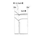
- FIG. 4 is a diagram showing an energy band and a carrier concentration in an IVA-IVA ′ cross section in FIG.
- FIG. 4 is a diagram showing an energy band and a carrier concentration in the IVB-IVB ′ cross section in FIG.
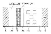
- FIG. 6 is a top surface layout diagram of a semiconductor device having a lateral HEMT according to a second embodiment of the present disclosure
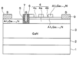
- FIG. 6 is a top surface layout diagram of a semiconductor device having a lateral HEMT according to a third embodiment of the present disclosure. It is sectional drawing of the semiconductor device which has horizontal type
- the semiconductor device according to the present embodiment is configured to include a lateral HEMT as a switching device.
- the horizontal HEMT of the present embodiment is formed using a structure in which an i-type, n-type, or p-type GaN layer 3 is laminated on the surface of a substrate 1 with a buffer layer 2 interposed therebetween as a compound semiconductor substrate.
- An AlGaN layer 4 in which a first AlGaN layer 4 a and a second AlGaN layer 4 b are stacked is formed on the surface of the GaN layer 3, and the GaN layer 3 and the AlGaN layer 4 constitute a heterojunction structure.
- the horizontal HEMT operates by using the GaN layer 3 and the AlGaN layer 4 as channel forming layers and inducing 2DEG carriers on the GaN layer 3 side of the AlGaN / GaN interface by a piezoelectric effect and a spontaneous polarization effect.
- the substrate 1 is made of a semi-insulating material such as Si (111), SiC, or sapphire, or a semiconductor material, and a buffer layer 2 serving as a base film for forming a GaN layer 3 with good crystallinity thereon. Is formed.
- the buffer layer 2 is composed of, for example, an AlGaN-GaN superlattice layer. If the GaN layer 3 can be formed on the substrate 1 with good crystallinity, the buffer layer 2 may be omitted.
- the crystallinity means defects or dislocations in the GaN layer 3 and has an influence on electrical and optical characteristics.
- a GaN layer 3 and an AlGaN layer 4 are formed on the buffer layer 2 by, for example, heteroepitaxial growth.
- the GaN layer 3 constitutes an electron transit layer made of a GaN-based semiconductor material such as i-GaN, n-GaN or p-GaN.
- the AlGaN layer 4 is made of a semiconductor material having a bandgap energy larger than that of the GaN-based semiconductor material constituting the GaN layer 3, and constitutes a barrier layer serving as an electron supply unit.
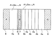
- the AlGaN layer 4 includes a first AlGaN layer 4a and a second AlGaN layer 4b, and a recess for embedding the gate structure so as to penetrate the first AlGaN layer 4a and the second AlGaN layer 4b. Part 5 is formed.
- the recess portion 5 has a line shape extending in one direction parallel to the surface of the substrate 1, specifically, the vertical direction of the paper surface of FIG. 2 (corresponding to the normal direction of the paper surface of FIG. 1).
- the first AlGaN layer 4a is composed of Al x Ga 1-x N, where the Al mixed crystal ratio is x
- the second AlGaN layer 4b is composed of Al y Ga 1-y N, where the Al mixed crystal ratio is y.
- the Al mixed crystal ratio x of the first AlGaN layer 4a is set larger than the Al mixed crystal ratio y of the second AlGaN layer 4b.
- 2DHG two-dimensional hole gas
- the relationship between the thickness of the AlGaN layer formed as a single layer and Ns is the relationship shown in FIG. 3, and when the thickness is small, Ns changes greatly, but when it reaches a certain thickness (region surrounded by a broken line in the figure), Ns.
- the first and second AlGaN layers 4a and 4b are not set in such a range that Ns greatly varies depending on their thickness, but are set to thicknesses such that Ns is uniquely determined by the Al mixed crystal ratio.
- the first AlGaN layer 4 a is formed on the entire upper surface of the substrate 1 and is removed at the recess portion 5.
- the second AlGaN layer 4b is disposed between the gate structure portion on the upper surface of the first AlGaN layer 4a and a drain electrode 9 described later, and is divided into a plurality of portions in the arrangement direction.
- the second AlGaN layer 4b is arranged at a constant interval from the recess portion 5, that is, from the side surface of the gate structure portion, and each second AlGaN layer 4b is in the vertical direction in FIG. It is made into the shape of a line extended to. For this reason, when each second AlGaN layer 4b is viewed from above, it is in a stripe shape.
- the width of each second AlGaN layer 4b is arbitrary, but is set to the same width in this embodiment.
- a gate electrode 7 is embedded via a gate insulating film 6 as a gate structure portion. Specifically, a gate insulating film 6 having a predetermined film thickness is formed on the inner wall surface of the recess portion 5, and a gate electrode 7 is further formed on the gate insulating film 6 to constitute a gate structure portion. Has been.
- the gate insulating film 6 is made of a silicon oxide film (SiO 2 ), alumina (Al 2 O 3 ) or the like, and the gate electrode 7 is made of a metal such as aluminum or platinum or a poly-semiconductor doped with impurities. It is configured. By forming the gate insulating film 6 and the gate electrode 7 in the recess portion 5, a MOS structure gate structure portion is formed.
- a source electrode 8 and a drain electrode 9 are formed on both sides of the surface of the first AlGaN layer 4a with the gate structure interposed therebetween so as to be separated from the second AlGaN layer 4b.
- the source electrode 8 and the drain electrode 9 are in ohmic contact with the first AlGaN layer 4a.
- a gate wiring layer, a source wiring layer, and a drain wiring layer made of Al or the like are formed on the surfaces of the gate electrode 7, the source electrode 8, and the drain electrode 9, respectively. These are electrically separated through an interlayer insulating film, and an arbitrary voltage can be applied to each electrode.
- a heterojunction structure is formed by the GaN layer 3 and the AlGaN layer 4, and the AlGaN layer 4 is formed by the first and second AlGaN layers 4a and 4b having different Al mixed crystal ratios.
- the lower AlAl layer 4a is made to have a higher Al crystal ratio than the upper AlGaN layer 4b, and the second AlGaN layer 4b is divided into a plurality of parts between the gate structure portion and the drain electrode 9.
- the structure is arranged.
- the thicknesses of the first and second AlGaN layers 4a and 4b are set to such a thickness that Ns is uniquely determined by the Al mixed crystal ratio. Therefore, in the thermal equilibrium state, the energy band and carrier concentration in the IVA-IVA ′ section and the IVB-IVB ′ section in FIG. 1 are as shown in FIGS. 4A and 4B.
- the energy bands of the conduction band and the valence band at the boundary between the first AlGaN layer 4a and the GaN layer 3 are The shape protrudes downward. Then, based on + (positive) fixed charges that are present in contact with the GaN layer 3 in the first AlGaN layer 4a, ⁇ (negative) charges are collected in the surface layer portion of the GaN layer 3. Therefore, the carrier concentration, that is, Ns increases.
- the second AlGaN layer 4b is affected by the second AlGaN layer 4b and the second AlGaN layer 4b A negative fixed charge is induced in the surface layer portion of the 1AlGaN layer 4a. That is, since the Al mixed crystal ratio of the second AlGaN layer 4b is smaller than that of the first AlGaN layer 4a, a negative fixed charge is induced in the surface layer portion of the first AlGaN layer 4a.
- the Al mixed crystal ratio of the second AlGaN layer 4b is set to a value that does not generate a two-dimensional hole gas (hereinafter referred to as 2DHG). Therefore, the value obtained by subtracting the minus fixed charge from the plus fixed charge in the first AlGaN layer 4a is smaller than that in the case of FIG. 4A, and the charge concentration Ns due to the minus electrons collected in the surface layer portion of the GaN layer 3 is reduced. Less.
- a channel portion of 2DEG is formed in the surface layer portion of the GaN layer 3 as shown in FIG. 5B. Thereby, a current flows between the source and the drain.
- the number of electrons serving as carriers is smaller than in the part where only the first AlGaN layer 4a is formed. Therefore, if the range in which the second AlGaN layer 4b is formed is wide, the on-resistance is increased.
- the second AlGaN layer 4 b is formed only from the side surface of the recess portion 5 with a predetermined width, and is not formed in the vicinity of the source electrode 8 and the drain electrode 9. For this reason, it is possible to suppress an increase in on-resistance as much as possible.
- the AlGaN layer 4 is the first AlGaN layer 4a and the second AlGaN layer 4b, and the upper second AlGaN layer 4b is divided into a plurality of parts between the gate structure portion and the drain electrode 9.
- the Al mixed crystal ratio x of the first AlGaN layer 4a is set to be larger than the Al mixed crystal ratio y of the second AlGaN layer 4b.
- the area of the second AlGaN layer 4b is small.
- reducing the area of the second AlGaN layer 4b affects the breakdown voltage.
- the area ratio of the portion where only the single layer of the first AlGaN layer 4a is disposed and the portion where the second AlGaN layer 4b is disposed is used as a design parameter so that the on-resistance can be reduced while ensuring a desired breakdown voltage. It is preferable to perform the design.
- the manufacturing method of the semiconductor device configured as described above is basically the same as the conventional method, but the formation process of the AlGaN layer 4 is different from the conventional method.
- the second AlGaN layer 4b is etched using a desired mask. As a result, the second AlGaN layer 4b remains only in the vicinity of the region where the gate structure portion is to be formed.
- the recess portion 5 is formed by performing etching using a desired mask so as to penetrate the first AlGaN layer 4a and reach the GaN layer 3 from the surface of the second AlGaN layer 4b.
- a gate structure part is formed by performing a gate insulating film formation process, a gate electrode embedding process, a patterning process, and the like. Then, the semiconductor device of this embodiment can be manufactured by performing the formation process of an interlayer insulation film, the formation process of the source electrode 8 and the drain electrode 9, etc.
- Ns is not adjusted by adjusting the film thickness of the first and second AlGaN layers 4a and 4b by etching, so that a large fluctuation of Ns due to the film thickness adjustment does not occur. Stable device characteristics with good controllability can be expected.
- a very thin layer of AlN that does not generate carriers may be inserted between the first AlGaN layer 4a and the second AlGaN layer 4b, and used as an etch stopper when etching the second AlGaN layer 4b.
- the portion of the second AlGaN layer 4b that is in contact with the gate structure portion is formed in a line shape, but the portion separated from the gate structure portion is formed in the second AlGaN layer 4b in a line shape.
- the structure is arranged in a dot shape.
- the second AlGaN layer 4b is divided not only on the line along the horizontal direction in FIG. 8 but also on the line along the vertical direction, and the second AlGaN layer 4b is arranged in a mesh shape, in other words, an island shape. It has a structure.
- the area of the second AlGaN layer 4b can be reduced as compared with the first embodiment.
- Ns becomes low, which causes an increase in on-resistance. For this reason, it is possible to reduce the on-resistance by arranging the second AlGaN layer 4b in a mesh pattern and reducing the area where Ns is lowered as in the present embodiment.
- the portion of the second AlGaN layer 4b that is in contact with the gate structure portion is formed in a line shape, but the second AlGaN layer 4b is formed in a dot shape for the portion away from the gate structure portion.
- the structure is arranged.
- the second AlGaN layer 4b is not divided on the line extending in the y direction as in the second embodiment, but is arranged in a staggered manner.
- the area of the second AlGaN layer 4b can be further reduced as compared with the second embodiment. For this reason, the on-resistance can be further reduced.
- a third AlGaN layer 4c is provided between the first AlGaN layer 4a and the second AlGaN layer 4b.
- the 3AlGaN layer 4c is an Al mole fraction as z, is composed of Al z Ga 1-z N.
- the Al mixed crystal ratio z of the third AlGaN layer 4c is made larger than the Al mixed crystal ratio x of the first AlGaN layer 4a and the Al mixed crystal ratio y of the second AlGaN layer 4b.
- the film thickness of the third AlGaN layer 4c is made thinner than the film thickness of the first AlGaN layer 4a and the second AlGaN layer 4b.
- the third AlGaN layer 4c is provided between the first AlGaN layer 4a and the second AlGaN layer 4b.
- the etching rate of the AlGaN layer varies depending on the Al mixed crystal ratio. The higher the Al mixed crystal ratio, the lower the etching rate. For this reason, in the manufacturing process of the semiconductor device, the third AlGaN layer 4c can be used as an etch stopper when the second AlGaN layer 4b is patterned by etching. As a result, the second AlGaN layer 4b can be patterned without more reliably etching the first AlGaN layer 4a.
- the semiconductor device has an operation region 100 in which an element operation is performed by forming a horizontal HEMT, that is, an element formation region, and an element isolation region 200 provided on the outside thereof. . Since Ns changes abruptly at the interface between the element isolation region 200 and the operation region 100, the electric field is most easily concentrated.
- the area of the second AlGaN layer 4b increases as the element isolation region 200 is closer. Specifically, as shown in FIG. 11, the closer to the element isolation region 200, the larger the number of second AlGaN layers 4 b that are divided, and the position away from the element isolation region 200, that is, the inside of the operation region 100. At the position, the number of the second AlGaN layers 4b is a constant number smaller than that.
- the depth of the recess portion 5 is set to a depth at which the surface of the GaN layer 3 is exposed, but this is merely an example.
- the recess portion 5 may have a depth until the surface layer portion of the GaN layer 3 is partially removed, or a portion of the first AlGaN layer 4a remains to the extent that no 2DEG carriers are formed on the bottom surface of the recess portion 5. It may be the depth of.
- the second AlGaN layer 4b is provided only between the gate structure and the drain electrode 9, and no second AlGaN layer 4b is formed between the gate structure and the source electrode 8.
- a second AlGaN layer 4b having a predetermined width may be formed from the side surface of the gate structure portion between the gate structure portion and the source electrode 8.
Landscapes
- Junction Field-Effect Transistors (AREA)
- Insulated Gate Type Field-Effect Transistor (AREA)
Abstract
半導体装置において、AlGaN層(4)が第1AlGaN層(4a)および第2AlGaN層(4b)を有する。第2AlGaN層はゲート構造部とドレイン電極(9)との間に配置され、ゲート構造部とドレイン電極との配列方向において複数に分割されている。第2AlGaN層の第2Al混晶比は、第1AlGaN層の第1Al混晶比よりも小さくされている。これにより、ノーマリーオフのデバイスとしつつ、阻止耐圧の低下を抑制でき、かつ、オン抵抗の上昇を抑制することが可能な半導体装置を提供することができる。
Description
本出願は、2015年7月10日に出願された日本出願番号2015-138957号に基づくもので、ここにその記載内容を援用する。
本開示は、窒化物半導体である窒化ガリウム(以下、GaNという)と窒化アルミニウムガリウム(以下、AlGaNという)とによるヘテロジャンクション構造を有する半導体装置に関するものである。
従来、特許文献1において、ヘテロジャンクション構造を有した横型のスイッチングデバイスとして、電界効果トランジスタであるHEMT(High electron mobility transistor:高電子移動度トランジスタ)を備えた半導体装置が提案されている。
この半導体装置には、GaNとAlGaNとによるヘテロジャンクション構造を有する横型のHEMTが備えられている。具体的には、基板の上にGaN電子走行層とAlGaN電子供給層とを順に積層したGaN系半導体層を備えている。AlGaN電子供給層は、リセス部が形成されることで厚みが薄くされており、リセス部内にゲート電極が備えられ、ゲート電極を挟んだ両側において、AlGaN電子供給層の上にソース電極およびドレイン電極が形成されている。リセス部は、ゲート電極が配置されるゲート埋込部に加えて、ゲート埋込部よりも外側にも設けられており、ゲート埋込部よりもソース側に第1リセス部が設けられ、ドレイン側に第2リセス部が設けられている。
このように構成されるHEMTでは、ゲート電極の両側に位置するAlGaN電子供給層の下方において、ピエゾ効果および自発分極効果による2次元電子ガス(以下、2DEGという)キャリアを誘起する。そして、ゲート電極の下方位置におけるGaN電子走行層の表層部をチャネル部として、2DEGキャリアおよびチャネル部を通じてソース-ドレイン間に電流を流すという動作を行う。
このようなHEMTにおいて、リセス部を設けることでAlGaN電子供給層を薄くしている。これにより、AlGaN電子供給層のうちリセス部が形成された部分にてそれより厚い部分よりも応力を緩和させられ、ピエゾ分極発生を抑制することができ、2DEG濃度(以下、Nsという)を少なくできる。したがって、阻止耐圧を低下させないようにすることができる。また、AlGaN電子供給層を部分的に複数箇所において薄くする構造とすることもでき、そのような構造とすれば更に最大電界強度を減らすことが可能となる。
しかしながら、AlGaN電子供給層の膜厚と応力との関係にはほぼ臨界性があることが確認されており、Nsの膜厚に対する感度は非常に高い(後述する図3参照)。したがって、AlGaN電子供給層の膜厚が少し異なっただけでNsが大きく変わり、Nsの制御が難しいという問題がある。AlGaN電子供給層の膜厚については、エッチングによって薄くすることになるが、エッチングによる膜厚制御は難しく、Nsを制御することが難しい。
本開示は、ノーマリーオフのデバイスとしつつ、制御性よく阻止耐圧の低下を抑制でき、かつ、オン抵抗の上昇を抑制することが可能な半導体装置を提供することを目的とする。
本開示の一態様によれば、半導体装置は、横型のスイッチングデバイスを備えている。スイッチングデバイスは、基板と、チャネル形成層と、ゲート構造部と、ソース電極と、ドレイン電極と、を有する。基板は、半絶縁体もしくは半導体にて構成される。チャネル形成層は、基板上に形成され、電子走行層を構成するGaN層および電子供給部を構成するAlGaN層によるヘテロジャンクション構造を有し、AlGaN層が部分的に除去されたリセス部が形成されている。ゲート構造部は、リセス部内に形成されたゲート絶縁膜および該ゲート絶縁膜の上に形成されたゲート電極を有して構成される。ソース電極およびドレイン電極は、チャネル形成層上において、ゲート構造部を挟んだ両側に配置される。スイッチングデバイスでは、GaN層とAlGaN層との界面におけるGaN層側に2次元電子ガスキャリアが誘起されると共に、ゲート電極に対して電圧が印加されたときにリセス部の底部におけるGaN層の表面部にチャネルが形成されることで、ソース電極とドレイン電極との間に電流が流れる。このような構成において、AlGaN層は、第1AlGaN層と第2AlGaN層を有する。第1AlGaN層は、第1AlGaN層の2次元電子ガス濃度を決める第1Al混晶比に設定される。第2AlGaN層は、ゲート構造部とドレイン電極との間に配置され、ゲート構造部とドレイン電極との配列方向において複数に分割される。第2AlGaN層は、第2AlGaN層の2次元電子ガス濃度を決める第2Al混晶比に設定される。第2Al混晶比が第1Al混晶比よりも小さくされることで、第2AlGaN層が負の固定電荷を誘起する。
このような構成とすることで、ノーマリーオフのデバイスとしつつ、阻止耐圧の低下を抑制でき、かつ、オン抵抗の上昇を抑制することが可能な半導体装置とすることができる。
本開示についての上記目的およびその他の目的、特徴や利点は、添付の図面を参照しながら下記の詳細な記述により、より明確になる。図面において、
本開示の第1実施形態にかかる横型のHEMTを有する半導体装置の断面図であり、
図1に示す半導体装置の上面レイアウト図であり、
Al混晶比、AlGaN層の厚みとNsとの関係を示した図であり、
図1中のIVA-IVA'断面でのエネルギーバンドおよびキャリア濃度を示した図であり、
図1中のIVB-IVB’断面でのエネルギーバンドおよびキャリア濃度を示した図であり、
阻止状態における横型のHEMTの空間電荷の分布を示した断面図であり、
オン状態における横型のHEMTの電子の分布を示した断面図であり、
第2AlGaN層を連続的に形成した場合に電界強度が高くなる部位を示した断面図であり、
第2AlGaN層を分割して形成した場合と連続的に形成した場合それぞれにおける電界強度分布を示した図であり、
本開示の第2実施形態にかかる横型のHEMTを有する半導体装置の上面レイアウト図であり、
本開示の第3実施形態にかかる横型のHEMTを有する半導体装置の上面レイアウト図であり、
本開示の第4実施形態にかかる横型のHEMTを有する半導体装置の断面図であり、
本開示の第5実施形態にかかる横型のHEMTを有する半導体装置の上面レイアウト図である。
以下、本開示の実施形態について図に基づいて説明する。なお、以下の各実施形態相互において、互いに同一もしくは均等である部分には、同一符号を付して説明を行う。
(第1実施形態)
図1を参照して、本実施形態にかかる半導体装置について説明する。図1に示すように、本実施形態にかかる半導体装置は、スイッチングデバイスとして横型のHEMTを備えた構成とされている。
図1を参照して、本実施形態にかかる半導体装置について説明する。図1に示すように、本実施形態にかかる半導体装置は、スイッチングデバイスとして横型のHEMTを備えた構成とされている。
本実施形態の横型のHEMTは、基板1の表面に、バッファ層2を介してi型、n型もしくはp型のGaN層3が積層された構造を化合物半導体基板として用いて形成されている。GaN層3の表面には、第1AlGaN層4aおよび第2AlGaN層4bが積層されたAlGaN層4が形成されており、GaN層3とAlGaN層4によってヘテロジャンクション構造が構成されている。横型のHEMTは、これらGaN層3およびAlGaN層4をチャネル形成層として、AlGaN/GaN界面のGaN層3側に、ピエゾ効果および自発分極効果によって2DEGキャリアが誘起されることで動作する。
基板1は、Si(111)やSiCもしくはサファイヤなどの半絶縁性材料や半導体材料によって構成されており、この上にGaN層3を結晶性良く成膜するための下地膜となるバッファ層2が形成されている。バッファ層2は、例えばAlGaN-GaN超格子層などによって構成されている。基板1の上に結晶性良くGaN層3が成膜できる場合には、バッファ層2は無くても構わない。なお、ここでの結晶性とは、GaN層3中の欠陥や転位などであり、電気的および光学的な特性に対して影響を及ぼすものを意味している。
バッファ層2の上には、GaN層3とAlGaN層4が例えばヘテロエピタキシャル成長によって形成されている。
GaN層3は、i-GaN、n-GaNもしくはp-GaNのGaN系の半導体材料で構成された電子走行層を構成するものである。
AlGaN層4は、GaN層3を構成するGaN系半導体材料よりもバンドギャップエネルギーの大きな半導体材料で構成されたものであり、電子供給部となるバリア層を構成している。本実施形態の場合、AlGaN層4を第1AlGaN層4aと第2AlGaN層4bとを有した構成としており、これら第1AlGaN層4aと第2AlGaN層4bを貫通するようにゲート構造部の埋め込み用のリセス部5が形成されている。リセス部5は、基板1の表面に対して平行な一方向、具体的には図2の紙面上下方向(図1の紙面法線方向に相当)に延設されたライン状とされている。
第1AlGaN層4aは、Al混晶比をxとして、AlxGa1-xNで構成され、第2AlGaN層4bは、Al混晶比をyとして、AlyGa1-yNで構成されている。第1AlGaN層4aのAl混晶比xは、第2AlGaN層4bのAl混晶比yよりも大きくされている。このように、第1AlGaN層4aおよび第2AlGaN層4bのAl混晶比x、yを設定することで、2次元ホールガス(以下、2DHGという)を発生させずに負の固定電荷を誘起することが可能となる。これら第1、第2AlGaN層4a、4bは、共に、Ns(2DEG濃度)がAl混晶比によって一義的に決まる厚みに設定されている。
すなわち、単層で形成したAlGaN層の厚みとNsとの関係は図3に示す関係となり、厚みが薄いとNsが大きく変化するが、ある程度の厚み(図中破線で囲んだ領域)になるとNsがAlGaN層の厚みに依存するのではなく、Al混晶比によって一義的に決まる。したがって、第1、第2AlGaN層4a、4bについては、これらの厚みによってNsが大きく変動する範囲ではなく、Al混晶比によって一義的にNsが決まる程度の厚みに設定してある。
第1AlGaN層4aは、基板1の上面の全面に形成されており、リセス部5において除去されている。第2AlGaN層4bは、第1AlGaN層4aの上面のうちのゲート構造部と後述するドレイン電極9との間に配置され、これらの配列方向において複数に分割されて形成されている。本実施形態の場合、第2AlGaN層4bは、リセス部5から、つまりゲート構造部の側面から一定間隔で配置されており、各第2AlGaN層4bはリセス部5と同様に図3の紙面上下方向に延設されたライン状とされている。このため、各第2AlGaN層4bを上面から見るとストライプ状になっている。各第2AlGaN層4bの幅については任意であるが、本実施形態では同幅に設定してある。
リセス部5内には、ゲート構造部として、ゲート絶縁膜6を介してゲート電極7が埋め込まれている。具体的には、リセス部5の内壁面に所定膜厚のゲート絶縁膜6が成膜されており、このゲート絶縁膜6の上に更にゲート電極7が形成されることでゲート構造部が構成されている。
ゲート絶縁膜6は、シリコン酸化膜(SiO2)やアルミナ(Al2O3)などによって構成されており、ゲート電極7は、アルミニウム、プラチナなどの金属または不純物がドープされたPoly-半導体などによって構成されている。これらゲート絶縁膜6およびゲート電極7をリセス部5内に形成することでMOS構造のゲート構造部を構成している。
一方、第1AlGaN層4aの表面のうちゲート構造部を挟んだ両側それぞれにおいて、第2AlGaN層4bからは離れるようにソース電極8とドレイン電極9が形成されている。そして、ソース電極8やドレイン電極9が第1AlGaN層4aに対してそれぞれオーミック接触させられている。このような構成により、本実施形態にかかる横型のHEMTが構成されている。
なお、図示していないが、ゲート電極7やソース電極8およびドレイン電極9の表面には、それぞれ、Alなどで構成されるゲート配線層やソース配線層およびドレイン配線層が形成されている。これらは、層間絶縁膜を介して電気的に分離されており、各電極に任意の電圧が印加できるようになっている。
このように、本実施形態の半導体装置では、GaN層3とAlGaN層4によるヘテロジャンクション構造を構成し、AlGaN層4をAl混晶比の異なる第1、第2AlGaN層4a、4bによって構成している。そして、下層側の第1AlGaN層4aの方が上層側の第2AlGaN層4bよりもAl混晶比が大きくなるようにし、第2AlGaN層4bをゲート構造部とドレイン電極9との間において複数に分割して配置した構造としている。
そして、第1、第2AlGaN層4a、4bの厚みをNsがAl混晶比によって一義的に決まる程度の厚みに設定している。このため、熱平衡状態において、図1中のIVA-IVA'断面やIVB-IVB’断面でのエネルギーバンドおよびキャリア濃度は、図4Aおよび図4Bのようになる。
すなわち、図4Aに示すように、GaN層3上に第1AlGaN層4aのみが形成されている部分では、第1AlGaN層4aとGaN層3との境界部における伝導帯および価電子帯のエネルギーバンドが下方に向けて突出した形状となる。そして、第1AlGaN層4a中のGaN層3に接して多く存在している+(正)の固定電荷に基づいて、GaN層3の表層部に-(負)の電荷が集まった状態となる。したがって、キャリア濃度、すなわちNsが大きくなる。
一方、図4Bに示すように、GaN層3上に第1、第2AlGaN層4a、4bが形成されている部分では、第2AlGaN層4bの影響で、第2AlGaN層4bとの境界部において、第1AlGaN層4aの表層部に-の固定電荷が誘起される。つまり、第2AlGaN層4bの方が第1AlGaN層4aよりもAl混晶比が小さくされているため、第1AlGaN層4aの表層部に-の固定電荷を誘起させる。かつ第2AlGaN層4bのAl混晶比は2次元ホールガス(以下、2DHGという)を発生させない程度の値としている。このため、第1AlGaN層4a内の+の固定電荷から-の固定電荷分を差し引いた値が図4Aの場合と比較して小さくなり、GaN層3の表層部に集まる-の電子による電荷濃度Nsが少なくなる。
阻止状態においては、図5Aに示すように固定電荷が作用する。具体的には、第1AlGaN層4a上に第2AlGaN層4bが形成されている部位では、第1AlGaN層4aの表層部に-の固定電荷があることで下方位置の+の固定電荷が実効的に相殺され、これによりゲート近傍の領域の電界強度が弱められる。一方、GaN層3の上に第1AlGaN層4aしか形成されていない部位では、多く存在する+の固定電荷によってドレイン近傍の領域の電界強度が弱くなる。したがって、局所的な電界強度の強い部分がなくなることにより耐圧向上を図ることが可能となる。また、ゲート構造部の下方においては2DEGが形成されていないことから、ノーマリーオフのデバイスとなる。
また、オン状態(導通状態)においては、図5Bに示すようにGaN層3の表層部に2DEGによるチャネル部が形成される。これにより、ソース-ドレイン間に電流が流れる。このとき、第1AlGaN層4aの上に第2AlGaN層4bが形成された部位では、第1AlGaN層4aのみの部位と比較して、キャリアとなる電子の数(2DEGキャリアの数)が少なくなる。したがって、第2AlGaN層4bが形成されている範囲が広いと、オン抵抗を増大させることになる。しかしながら、本実施形態の場合、第2AlGaN層4bをリセス部5の側面から所定の幅のみ形成するようにしており、ソース電極8やドレイン電極9の近傍には形成しないようにしている。このため、オン抵抗の増大をできるだけ抑制することが可能となる。
ここで、図6に示すように、第2AlGaN層4bをゲート構造部とドレイン電極9との間に連続的に1つのみ設ける構造も考えられる。しかしながら、このような構造とする場合、図7の実線で示したように、ゲート構造部と第2AlGaN層4bとの境界位置に加えて、図6中の一点差線で囲んだ領域、つまり第2AlGaN層4bのうちのドレイン電極9側の端部において、電界強度が高くなる。このため、第2AlGaN層4bを所望膜厚で形成することで制御性良く電界緩和が行えるようにするものの、第2AlGaN層4bのうちのドレイン電極9側の端部のように、Nsが急変する場所では電界集中が発生する。このため、耐圧向上効果が十分ではない。
これに対して、本実施形態のように、第2AlGaN層4bを複数に分割して配置した構造の場合、第2AlGaN層4bが分割された位置それぞれにおいてNsが急変することになる。このため、図7中の一点鎖線で示したように、電界強度が高くなる位置が複数になる。しかしながら、電界強度が高くなる場所を複数箇所にできることから、それぞれの場所での最大電界強度が小さくなる。したがって、図6に示すように第2AlGaN層4bを1つのみ設ける構造と比較して、さらに耐圧向上を図ることが可能となる。
以上説明したように、本実施形態では、AlGaN層4を第1AlGaN層4aおよび第2AlGaN層4bとし、上層側の第2AlGaN層4bについてはゲート構造部とドレイン電極9との間に複数に分割して配置した構造としている。そして、第1AlGaN層4aのAl混晶比xの方が第2AlGaN層4bのAl混晶比yよりも大きくなるようにしている。このような構成とすることで、ノーマリーオフのデバイスとしつつ、阻止耐圧の低下を抑制でき、かつ、オン抵抗の上昇を抑制することが可能な半導体装置とすることができる。
ただし、第2AlGaN層4bを形成することによってオン抵抗を増加させることになるため、第2AlGaN層4bの面積は少ない方が好ましい。その反面、第2AlGaN層4bの面積を少なくすると、耐圧に影響を及ぼす。このため、所望の耐圧を確保しつつ、オン抵抗を低減できるように、第1AlGaN層4aの単層のみが配置される部分と第2AlGaN層4bが配置される部分の面積比を設計パラメータとして用いて設計を行うのが好ましい。
なお、このように構成される半導体装置の製造方法は、基本的には従来と同様であるが、AlGaN層4の形成工程などが従来と異なったものとなる。
すなわち、GaN層3の上にAl混晶比を変えて第1AlGaN層4aと第2AlGaN層4bを順に積層したのち、所望のマスクを用いて第2AlGaN層4bをエッチングする。これにより、ゲート構造部の形成予定領域の近傍にのみ第2AlGaN層4bが残るようにする。
そして、第2AlGaN層4bの表面から第1AlGaN層4aを貫通してGaN層3に達するように所望のマスクを用いてエッチングを行うことでリセス部5を形成する。
さらに、ゲート絶縁膜形成工程、ゲート電極埋込およびパターニング工程などを行うことで、ゲート構造部を形成する。この後、層間絶縁膜の形成工程やソース電極8およびドレイン電極9の形成工程などを行うことで、本実施形態の半導体装置を製造することができる。
このような製造方法において、エッチングによって第1、第2AlGaN層4a、4bの膜厚調整などを行ってNsを調整することはないため、これらの膜厚調整に起因するNsの大きな変動は生じず、制御性よく安定したデバイス特性が期待できる。
第1AlGaN層4aと第2AlGaN層4bの間にはたとえばキャリアを生じない程度の非常に薄いAlNなどの層を挿入し、第2AlGaN層4bをエッチングする際のエッチストッパとして使用しても良い。
(第2実施形態)
本開示の第2実施形態について説明する。本実施形態は、第1実施形態に対してAlGaN層4の構成を変更したものであり、その他については第1実施形態と同様であるため、第1実施形態と異なる部分についてのみ説明する。
本開示の第2実施形態について説明する。本実施形態は、第1実施形態に対してAlGaN層4の構成を変更したものであり、その他については第1実施形態と同様であるため、第1実施形態と異なる部分についてのみ説明する。
図8に示すように、本実施形態では、第2AlGaN層4bのうちゲート構造部に接する部分についてはライン状としているが、ゲート構造部から離れたものについては、第2AlGaN層4bをライン状ではなく、ドット状に配置した構造としている。具体的には、図8中の左右方向に沿うライン上だけでなく上下方向に沿うライン上においても第2AlGaN層4bを分割し、第2AlGaN層4bを網目状、換言すれば島状に配置した構造としている。
このように、第2AlGaN層4bを網目状に配置すると、第1実施形態と比較して第2AlGaN層4bの面積を少なくすることができる。第2AlGaN層4bが形成された領域ではNsが低くなるため、オン抵抗の増加要因となる。このため、本実施形態のように第2AlGaN層4bを網目状に配置してNsが低くなる面積を少なくすることで、オン抵抗を低減することが可能となる。
(第3実施形態)
本開示の第3実施形態について説明する。本実施形態も、第1実施形態に対してAlGaN層4の構成を変更したものであり、その他については第1実施形態と同様であるため、第1実施形態と異なる部分についてのみ説明する。
本開示の第3実施形態について説明する。本実施形態も、第1実施形態に対してAlGaN層4の構成を変更したものであり、その他については第1実施形態と同様であるため、第1実施形態と異なる部分についてのみ説明する。
図9に示すように、本実施形態でも、第2AlGaN層4bのうちゲート構造部に接する部分についてはライン状としているが、ゲート構造部から離れたものについては、第2AlGaN層4bをドット状に配置した構造としている。ただし、第2実施形態のように、第2AlGaN層4bをy方向に延設されたライン上において分割する構造ではなく、千鳥状に配置した構造としている。
このように、第2AlGaN層4bを千鳥状に配置すると、第2実施形態と比較して更に第2AlGaN層4bの面積を少なくすることができる。このため、よりオン抵抗を低減することが可能となる。
(第4実施形態)
本開示の第4実施形態について説明する。本実施形態も、第1実施形態に対してAlGaN層4の構成を変更したものであり、その他については第1実施形態と同様であるため、第1実施形態と異なる部分についてのみ説明する。
本開示の第4実施形態について説明する。本実施形態も、第1実施形態に対してAlGaN層4の構成を変更したものであり、その他については第1実施形態と同様であるため、第1実施形態と異なる部分についてのみ説明する。
図10に示すように、本実施形態では、第1AlGaN層4aと第2AlGaN層4bの間に第3AlGaN層4cを備えている。第3AlGaN層4cは、Al混晶比をzとして、AlzGa1-zNで構成されている。第1AlGaN層4aのAl混晶比x、第2AlGaN層4bのAl混晶比yと比較して、第3AlGaN層4cのAl混晶比zは大きくされている。また、第3AlGaN層4cの膜厚は、第1AlGaN層4aや第2AlGaN層4bの膜厚よりも薄くされている。
このように、本実施形態では、第1AlGaN層4aと第2AlGaN層4bの間に第3AlGaN層4cを備えた構造としている。AlGaN層のエッチングレートは、Al混晶比によって変化し、Al混晶比が高いほどエッチングレートが低くなる。このため、半導体装置の製造工程において、第2AlGaN層4bをエッチングによってパターニングする際に、第3AlGaN層4cをエッチストッパして用いることができる。これにより、第1AlGaN層4aをより確実にエッチングすることなく、第2AlGaN層4bのパターンを行うことが可能となる。
(第5実施形態)
本開示の第5実施形態について説明する。本実施形態も、第1実施形態に対してAlGaN層4の構成を変更したものであり、その他については第1実施形態と同様であるため、第1実施形態と異なる部分についてのみ説明する。
本開示の第5実施形態について説明する。本実施形態も、第1実施形態に対してAlGaN層4の構成を変更したものであり、その他については第1実施形態と同様であるため、第1実施形態と異なる部分についてのみ説明する。
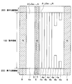
図11に示すように、半導体装置は、横型のHEMTが形成されることで素子動作が行われる動作領域100、つまり素子形成領域と、その外側に備えられる素子分離領域200とを有している。これら素子分離領域200と動作領域100との界面ではNsが急激に変化するため、電界が最も集中し易い。
このため、本実施形態では、素子分離領域200に近いほど第2AlGaN層4bの面積が増える構造としている。具体的には、図11に示すように、素子分離領域200に近いほど分割された第2AlGaN層4bの個数が多くなるようにし、素子分離領域200から離れた位置、つまり動作領域100の内側の位置では第2AlGaN層4bの個数をそれよりも少ない一定数としている。
このように、素子分離領域200に近づくほど第2AlGaN層4bの面積を増加させることにより、素子分離領域200と動作領域100との界面でのNsの変化を緩やかにすることが可能となる。このため、この界面近傍での電界強度を低下させることが可能となり、更に阻止耐圧を向上させることが可能となる。
(他の実施形態)
本開示は上記した実施形態に限定されるものではなく、本開示の要旨を逸脱しない範囲において適宜変更が可能である。
本開示は上記した実施形態に限定されるものではなく、本開示の要旨を逸脱しない範囲において適宜変更が可能である。
例えば、上記各実施形態では、リセス部5の深さを、GaN層3の表面が露出する深さとしたが、これは一例を示したに過ぎない。例えば、リセス部5をGaN層3の表層部が一部除去されるまでの深さとしても良いし、リセス部5の底面において2DEGキャリアが形成されない程度に第1AlGaN層4aの一部が残る程度の深さとされていても良い。
また、上記各実施形態では、ゲート構造部とドレイン電極9との間にのみ第2AlGaN層4bを備え、ゲート構造部とソース電極8との間には第2AlGaN層4bを全く形成していない構造を例に挙げた。これも一例を示したに過ぎず、例えばゲート構造部とソース電極8との間において、ゲート構造部の側面から所定幅の第2AlGaN層4bを形成した構造としても良い。
さらに、上記各実施形態で示した第2AlGaN層4bのレイアウトについても一例を示したのであり、他のレイアウトとしても良い。例えば。第2AlGaN層4bをドット状に配置する場合、網目状や千鳥状の配置する場合に限らない。
本開示は、実施例に準拠して記述されたが、本開示は当該実施例や構造に限定されるものではないと理解される。本開示は、様々な変形例や均等範囲内の変形をも包含する。加えて、様々な組み合わせや形態、さらには、それらに一要素のみ、それ以上、あるいはそれ以下、を含む他の組み合わせや形態をも、本開示の範疇や思想範囲に入るものである。
Claims (10)
- 半絶縁体もしくは半導体にて構成される基板(1)と、
前記基板上に形成され、電子走行層を構成するGaN層(3)および電子供給部を構成するAlGaN層(4)によるヘテロジャンクション構造を有し、前記AlGaN層が部分的に除去されたリセス部(5)が形成されたチャネル形成層と、
前記リセス部内に形成されたゲート絶縁膜(6)および該ゲート絶縁膜の上に形成されたゲート電極(7)を有して構成されるゲート構造部と、
前記チャネル形成層上において、前記ゲート構造部を挟んだ両側に配置されたソース電極(8)およびドレイン電極(9)と、を有し、
前記GaN層と前記AlGaN層との界面における前記GaN層側に2次元電子ガスキャリアが誘起されると共に、前記ゲート電極に対して電圧が印加されたときに前記リセス部の底部における前記GaN層の表面部にチャネルが形成されることで前記ソース電極と前記ドレイン電極との間に電流を流す横型のスイッチングデバイスを備え、
前記AlGaN層は、第1AlGaN層(4a)と、第2AlGaN層(4b)と、を有し、
前記第1AlGaN層は、前記第1AlGaN層の2次元電子ガス濃度を決める第1Al混晶比に設定され、
前記第2AlGaN層は、前記ゲート構造部と前記ドレイン電極との間に配置され、
前記第2AlGaN層は、前記ゲート構造部と前記ドレイン電極との配列方向において複数に分割され、
前記第2AlGaN層は、前記第2AlGaN層の2次元電子ガス濃度を決める第2Al混晶比に設定され、かつ、
前記第2Al混晶比が前記第1Al混晶比よりも小さくされることで、前記第2AlGaN層が負の固定電荷を誘起する半導体装置。 - 前記ゲート構造部と前記ソース電極および前記ドレイン電極は、前記基板の表面に対して平行な一方向に延設されたライン状とされ、
前記第2AlGaN層も、前記一方向に延設されたライン状とされている請求項1に記載の半導体装置。 - 前記ゲート構造部と前記ソース電極および前記ドレイン電極は、前記基板の表面に対して平行な一方向に延設されたライン状とされ、
前記第2AlGaN層は、ドット状に配置されている請求項1に記載の半導体装置。 - 前記第2AlGaN層は、前記一方向に沿って延設されるライン上において複数に分割されることで前記ドット状とされている請求項3に記載の半導体装置。
- 前記第2AlGaN層は、千鳥状に配置されることで前記ドット状とされている請求項3に記載の半導体装置。
- 前記AlGaN層は、前記第1AlGaN層と前記第2AlGaN層との間に配置される第3AlGaN層(4c)を有し、
該第3AlGaN層の第3Al混晶比が前記第1AlGaN層の第1Al混晶比より大きく、かつ、前記第2AlGaN層の第2Al混晶比よりも大きい請求項1ないし5のいずれか1つに記載の半導体装置。 - 前記スイッチングデバイスが形成されることで素子として動作する動作領域(100)と、
前記動作領域の外側に位置する素子分離領域(200)と、を有し、
前記第2AlGaN層は、前記素子分離領域に近づくほど形成面積が増加させられている請求項1ないし6のいずれか1つに記載の半導体装置。 - 前記第1AlGaN層の前記2次元電子ガス濃度は、前記第1Al混晶比が大きくなるにつれて、大きくなり、
前記第2AlGaN層の前記2次元電子ガス濃度は、前記第2Al混晶比が大きくなるにつれて、大きくなる請求項1ないし7のいずれか1つに記載の半導体装置。 - 前記第2AlGaN層は、前記ゲート構造部と前記ドレイン電極との配列方向において複数に分割され、かつ、互いに離間している請求項1ないし8のいずれか1つに記載の半導体装置。
- 第1AlGaN層が前記GaN層上に設けられ、
前記第2AlGaN層が前記第1AlGaN層上に設けられる請求項1ないし9のいずれか1つに記載の半導体装置。
Priority Applications (1)
| Application Number | Priority Date | Filing Date | Title |
|---|---|---|---|
| US15/573,200 US10062747B2 (en) | 2015-07-10 | 2016-06-14 | Semiconductor device |
Applications Claiming Priority (2)
| Application Number | Priority Date | Filing Date | Title |
|---|---|---|---|
| JP2015-138957 | 2015-07-10 | ||
| JP2015138957A JP6311668B2 (ja) | 2015-07-10 | 2015-07-10 | 半導体装置 |
Publications (1)
| Publication Number | Publication Date |
|---|---|
| WO2017010041A1 true WO2017010041A1 (ja) | 2017-01-19 |
Family
ID=57757302
Family Applications (1)
| Application Number | Title | Priority Date | Filing Date |
|---|---|---|---|
| PCT/JP2016/002872 Ceased WO2017010041A1 (ja) | 2015-07-10 | 2016-06-14 | 半導体装置 |
Country Status (3)
| Country | Link |
|---|---|
| US (1) | US10062747B2 (ja) |
| JP (1) | JP6311668B2 (ja) |
| WO (1) | WO2017010041A1 (ja) |
Families Citing this family (6)
| Publication number | Priority date | Publication date | Assignee | Title |
|---|---|---|---|---|
| JP7231824B2 (ja) * | 2019-03-29 | 2023-03-02 | 富士通株式会社 | 半導体装置、半導体装置の製造方法及び電子装置 |
| JP7332548B2 (ja) * | 2020-08-06 | 2023-08-23 | 株式会社東芝 | 半導体装置 |
| CN112768505B (zh) * | 2020-12-31 | 2023-02-10 | 西安电子科技大学 | 异质结功率器件及其制作方法 |
| US12575125B2 (en) | 2021-05-20 | 2026-03-10 | Wolfspeed, Inc. | Field effect transistor with selective modified access regions |
| JP7770424B2 (ja) * | 2021-05-20 | 2025-11-14 | ウルフスピード インコーポレイテッド | 修正アクセス領域を備える電界効果トランジスタ |
| CN113555429B (zh) * | 2021-07-06 | 2024-01-19 | 华南师范大学 | 高击穿电压和低导通电阻的常开hfet器件及其制备方法 |
Citations (4)
| Publication number | Priority date | Publication date | Assignee | Title |
|---|---|---|---|---|
| WO2012063329A1 (ja) * | 2010-11-10 | 2012-05-18 | 三菱電機株式会社 | 半導体装置、および半導体装置の製造方法 |
| JP2012186294A (ja) * | 2011-03-04 | 2012-09-27 | Sharp Corp | ノーマリオフ型ヘテロ接合電界効果トランジスタ |
| JP2013120854A (ja) * | 2011-12-07 | 2013-06-17 | Fujitsu Ltd | 化合物半導体装置及びその製造方法 |
| JP2013179128A (ja) * | 2012-02-28 | 2013-09-09 | Nagoya Univ | 電界効果トランジスタ |
Family Cites Families (8)
| Publication number | Priority date | Publication date | Assignee | Title |
|---|---|---|---|---|
| JP4002918B2 (ja) * | 2004-09-02 | 2007-11-07 | 株式会社東芝 | 窒化物含有半導体装置 |
| JP5093991B2 (ja) | 2005-03-31 | 2012-12-12 | 住友電工デバイス・イノベーション株式会社 | 半導体装置 |
| CN101604704B (zh) * | 2008-06-13 | 2012-09-05 | 西安能讯微电子有限公司 | Hemt器件及其制造方法 |
| JP2012054471A (ja) * | 2010-09-02 | 2012-03-15 | Fujitsu Ltd | 半導体装置及びその製造方法、電源装置 |
| EP2819152A4 (en) | 2012-02-23 | 2015-10-14 | Ngk Insulators Ltd | SEMICONDUCTOR ELEMENT AND MANUFACTURING METHOD FOR THE SEMICONDUCTOR ELEMENT |
| JP2013229458A (ja) | 2012-04-26 | 2013-11-07 | Mitsubishi Electric Corp | ヘテロ接合電界効果型トランジスタおよびその製造方法 |
| JP2014072379A (ja) | 2012-09-28 | 2014-04-21 | Fujitsu Ltd | 化合物半導体装置及びその製造方法 |
| JP6085442B2 (ja) * | 2012-09-28 | 2017-02-22 | トランスフォーム・ジャパン株式会社 | 化合物半導体装置及びその製造方法 |
-
2015
- 2015-07-10 JP JP2015138957A patent/JP6311668B2/ja not_active Expired - Fee Related
-
2016
- 2016-06-14 WO PCT/JP2016/002872 patent/WO2017010041A1/ja not_active Ceased
- 2016-06-14 US US15/573,200 patent/US10062747B2/en active Active
Patent Citations (4)
| Publication number | Priority date | Publication date | Assignee | Title |
|---|---|---|---|---|
| WO2012063329A1 (ja) * | 2010-11-10 | 2012-05-18 | 三菱電機株式会社 | 半導体装置、および半導体装置の製造方法 |
| JP2012186294A (ja) * | 2011-03-04 | 2012-09-27 | Sharp Corp | ノーマリオフ型ヘテロ接合電界効果トランジスタ |
| JP2013120854A (ja) * | 2011-12-07 | 2013-06-17 | Fujitsu Ltd | 化合物半導体装置及びその製造方法 |
| JP2013179128A (ja) * | 2012-02-28 | 2013-09-09 | Nagoya Univ | 電界効果トランジスタ |
Also Published As
| Publication number | Publication date |
|---|---|
| US10062747B2 (en) | 2018-08-28 |
| JP6311668B2 (ja) | 2018-04-18 |
| JP2017022270A (ja) | 2017-01-26 |
| US20180130873A1 (en) | 2018-05-10 |
Similar Documents
| Publication | Publication Date | Title |
|---|---|---|
| JP6332021B2 (ja) | 半導体装置 | |
| KR101813177B1 (ko) | 고전자이동도 트랜지스터 및 그 제조방법 | |
| JP4542912B2 (ja) | 窒素化合物半導体素子 | |
| JP6270572B2 (ja) | 半導体装置及びその製造方法 | |
| US8963207B2 (en) | Semiconductor device | |
| JP6439789B2 (ja) | 電界効果トランジスタ | |
| JP5261945B2 (ja) | 電界効果半導体装置及びその製造方法 | |
| KR101922122B1 (ko) | 노멀리 오프 고전자이동도 트랜지스터 | |
| JP5383652B2 (ja) | 電界効果トランジスタ及びその製造方法 | |
| KR102065113B1 (ko) | 고전자이동도 트랜지스터 및 그 제조 방법 | |
| KR101927410B1 (ko) | 고전자 이동도 트랜지스터 및 그 제조방법 | |
| KR101927408B1 (ko) | 고전자 이동도 트랜지스터 및 그 제조방법 | |
| JP6311668B2 (ja) | 半導体装置 | |
| JP2017073506A (ja) | 窒化物半導体装置およびその製造方法 | |
| JP2005244072A (ja) | 半導体装置 | |
| JP2009200395A (ja) | Hfetおよびその製造方法 | |
| CN104916633A (zh) | 半导体装置 | |
| KR20140011791A (ko) | 고전자이동도 트랜지스터 및 그 제조방법 | |
| CN104916679A (zh) | 半导体装置 | |
| JP2011082445A (ja) | 半導体装置およびその製造方法 | |
| JP2009278028A (ja) | 半導体装置 | |
| JP2016058721A (ja) | 半導体装置 | |
| JP6575224B2 (ja) | 半導体装置 | |
| KR102005451B1 (ko) | 고전자 이동도 트랜지스터 | |
| KR101887535B1 (ko) | 고전자 이동도 트랜지스터 및 그 제조방법 |
Legal Events
| Date | Code | Title | Description |
|---|---|---|---|
| 121 | Ep: the epo has been informed by wipo that ep was designated in this application |
Ref document number: 16824027 Country of ref document: EP Kind code of ref document: A1 |
|
| WWE | Wipo information: entry into national phase |
Ref document number: 15573200 Country of ref document: US |
|
| NENP | Non-entry into the national phase |
Ref country code: DE |
|
| 122 | Ep: pct application non-entry in european phase |
Ref document number: 16824027 Country of ref document: EP Kind code of ref document: A1 |