WO2016199632A1 - 光電変換素子、光電変換素子の製造方法および固体撮像装置 - Google Patents
光電変換素子、光電変換素子の製造方法および固体撮像装置 Download PDFInfo
- Publication number
- WO2016199632A1 WO2016199632A1 PCT/JP2016/066147 JP2016066147W WO2016199632A1 WO 2016199632 A1 WO2016199632 A1 WO 2016199632A1 JP 2016066147 W JP2016066147 W JP 2016066147W WO 2016199632 A1 WO2016199632 A1 WO 2016199632A1
- Authority
- WO
- WIPO (PCT)
- Prior art keywords
- group
- photoelectric conversion
- groups
- conversion element
- electrode
- Prior art date
Links
- 238000006243 chemical reaction Methods 0.000 title claims abstract description 171
- 238000000034 method Methods 0.000 title claims description 46
- 238000003384 imaging method Methods 0.000 title claims description 43
- 238000004519 manufacturing process Methods 0.000 title claims description 26
- 239000004065 semiconductor Substances 0.000 claims abstract description 62
- 239000000463 material Substances 0.000 claims description 72
- PMJMHCXAGMRGBZ-UHFFFAOYSA-N subphthalocyanine Chemical class N1C(N=C2C3=CC=CC=C3C(=N3)N2)=C(C=CC=C2)C2=C1N=C1C2=CC=CC=C2C3=N1 PMJMHCXAGMRGBZ-UHFFFAOYSA-N 0.000 claims description 49
- 125000004435 hydrogen atom Chemical group [H]* 0.000 claims description 15
- 229910052751 metal Inorganic materials 0.000 claims description 12
- 239000002184 metal Substances 0.000 claims description 12
- 125000001424 substituent group Chemical group 0.000 claims description 12
- 125000002887 hydroxy group Chemical group [H]O* 0.000 claims description 10
- -1 silylalkoxy groups Chemical group 0.000 claims description 10
- XOLBLPGZBRYERU-UHFFFAOYSA-N tin dioxide Chemical compound O=[Sn]=O XOLBLPGZBRYERU-UHFFFAOYSA-N 0.000 claims description 10
- 125000001153 fluoro group Chemical group F* 0.000 claims description 9
- ZOXJGFHDIHLPTG-UHFFFAOYSA-N Boron Chemical group [B] ZOXJGFHDIHLPTG-UHFFFAOYSA-N 0.000 claims description 8
- 229910052796 boron Inorganic materials 0.000 claims description 8
- HTXDPTMKBJXEOW-UHFFFAOYSA-N dioxoiridium Chemical compound O=[Ir]=O HTXDPTMKBJXEOW-UHFFFAOYSA-N 0.000 claims description 8
- 229910052731 fluorine Inorganic materials 0.000 claims description 8
- GYHNNYVSQQEPJS-UHFFFAOYSA-N Gallium Chemical compound [Ga] GYHNNYVSQQEPJS-UHFFFAOYSA-N 0.000 claims description 6
- 229910006404 SnO 2 Inorganic materials 0.000 claims description 6
- GWEVSGVZZGPLCZ-UHFFFAOYSA-N Titan oxide Chemical compound O=[Ti]=O GWEVSGVZZGPLCZ-UHFFFAOYSA-N 0.000 claims description 6
- HCHKCACWOHOZIP-UHFFFAOYSA-N Zinc Chemical compound [Zn] HCHKCACWOHOZIP-UHFFFAOYSA-N 0.000 claims description 6
- XLOMVQKBTHCTTD-UHFFFAOYSA-N Zinc monoxide Chemical compound [Zn]=O XLOMVQKBTHCTTD-UHFFFAOYSA-N 0.000 claims description 6
- 125000003277 amino group Chemical group 0.000 claims description 6
- 125000003118 aryl group Chemical group 0.000 claims description 6
- 229910052801 chlorine Inorganic materials 0.000 claims description 6
- 229910052733 gallium Inorganic materials 0.000 claims description 6
- 229910052738 indium Inorganic materials 0.000 claims description 6
- APFVFJFRJDLVQX-UHFFFAOYSA-N indium atom Chemical compound [In] APFVFJFRJDLVQX-UHFFFAOYSA-N 0.000 claims description 6
- AMGQUBHHOARCQH-UHFFFAOYSA-N indium;oxotin Chemical compound [In].[Sn]=O AMGQUBHHOARCQH-UHFFFAOYSA-N 0.000 claims description 6
- 229910001887 tin oxide Inorganic materials 0.000 claims description 6
- 229910052725 zinc Inorganic materials 0.000 claims description 6
- 239000011701 zinc Substances 0.000 claims description 6
- YVTHLONGBIQYBO-UHFFFAOYSA-N zinc indium(3+) oxygen(2-) Chemical compound [O--].[Zn++].[In+3] YVTHLONGBIQYBO-UHFFFAOYSA-N 0.000 claims description 6
- NGNBDVOYPDDBFK-UHFFFAOYSA-N 2-[2,4-di(pentan-2-yl)phenoxy]acetyl chloride Chemical group CCCC(C)C1=CC=C(OCC(Cl)=O)C(C(C)CCC)=C1 NGNBDVOYPDDBFK-UHFFFAOYSA-N 0.000 claims description 5
- 125000003504 2-oxazolinyl group Chemical group O1C(=NCC1)* 0.000 claims description 5
- 125000003903 2-propenyl group Chemical group [H]C([*])([H])C([H])=C([H])[H] 0.000 claims description 5
- 125000002252 acyl group Chemical group 0.000 claims description 5
- 125000004442 acylamino group Chemical group 0.000 claims description 5
- 125000004423 acyloxy group Chemical group 0.000 claims description 5
- 125000003545 alkoxy group Chemical group 0.000 claims description 5
- 125000003282 alkyl amino group Chemical group 0.000 claims description 5
- 125000004390 alkyl sulfonyl group Chemical group 0.000 claims description 5
- 125000003368 amide group Chemical group 0.000 claims description 5
- 125000000129 anionic group Chemical group 0.000 claims description 5
- 125000001769 aryl amino group Chemical group 0.000 claims description 5
- 125000005104 aryl silyl group Chemical group 0.000 claims description 5
- 125000004391 aryl sulfonyl group Chemical group 0.000 claims description 5
- 125000004069 aziridinyl group Chemical group 0.000 claims description 5
- 229910052794 bromium Inorganic materials 0.000 claims description 5
- VPKDCDLSJZCGKE-UHFFFAOYSA-N carbodiimide group Chemical group N=C=N VPKDCDLSJZCGKE-UHFFFAOYSA-N 0.000 claims description 5
- 125000002915 carbonyl group Chemical group [*:2]C([*:1])=O 0.000 claims description 5
- 125000003178 carboxy group Chemical group [H]OC(*)=O 0.000 claims description 5
- 125000004218 chloromethyl group Chemical group [H]C([H])(Cl)* 0.000 claims description 5
- 125000004093 cyano group Chemical group *C#N 0.000 claims description 5
- 125000006165 cyclic alkyl group Chemical group 0.000 claims description 5
- 125000004185 ester group Chemical group 0.000 claims description 5
- 125000003709 fluoroalkyl group Chemical group 0.000 claims description 5
- 125000002485 formyl group Chemical group [H]C(*)=O 0.000 claims description 5
- 125000003055 glycidyl group Chemical group C(C1CO1)* 0.000 claims description 5
- 150000004820 halides Chemical group 0.000 claims description 5
- 125000005843 halogen group Chemical group 0.000 claims description 5
- 229910052739 hydrogen Inorganic materials 0.000 claims description 5
- 239000001257 hydrogen Substances 0.000 claims description 5
- 229910052740 iodine Inorganic materials 0.000 claims description 5
- IQPQWNKOIGAROB-UHFFFAOYSA-N isocyanate group Chemical group [N-]=C=O IQPQWNKOIGAROB-UHFFFAOYSA-N 0.000 claims description 5
- 125000002560 nitrile group Chemical group 0.000 claims description 5
- 125000000449 nitro group Chemical group [O-][N+](*)=O 0.000 claims description 5
- 125000005010 perfluoroalkyl group Chemical group 0.000 claims description 5
- 125000001997 phenyl group Chemical group [H]C1=C([H])C([H])=C(*)C([H])=C1[H] 0.000 claims description 5
- 125000005353 silylalkyl group Chemical group 0.000 claims description 5
- 125000000472 sulfonyl group Chemical group *S(*)(=O)=O 0.000 claims description 5
- 125000004001 thioalkyl group Chemical group 0.000 claims description 5
- 125000005000 thioaryl group Chemical group 0.000 claims description 5
- 125000000391 vinyl group Chemical group [H]C([*])=C([H])[H] 0.000 claims description 5
- 150000008065 acid anhydrides Chemical class 0.000 claims description 4
- 125000002897 diene group Chemical group 0.000 claims description 4
- 239000010410 layer Substances 0.000 description 89
- 239000000126 substance Substances 0.000 description 35
- 230000004044 response Effects 0.000 description 32
- 230000000052 comparative effect Effects 0.000 description 21
- 239000010408 film Substances 0.000 description 18
- 238000012545 processing Methods 0.000 description 16
- 239000000758 substrate Substances 0.000 description 16
- 239000000969 carrier Substances 0.000 description 11
- 238000005259 measurement Methods 0.000 description 11
- 238000004544 sputter deposition Methods 0.000 description 9
- IJGRMHOSHXDMSA-UHFFFAOYSA-N Atomic nitrogen Chemical compound N#N IJGRMHOSHXDMSA-UHFFFAOYSA-N 0.000 description 8
- 238000010494 dissociation reaction Methods 0.000 description 8
- 230000005593 dissociations Effects 0.000 description 8
- 238000001771 vacuum deposition Methods 0.000 description 7
- 230000003287 optical effect Effects 0.000 description 6
- 230000035945 sensitivity Effects 0.000 description 6
- XUIMIQQOPSSXEZ-UHFFFAOYSA-N Silicon Chemical compound [Si] XUIMIQQOPSSXEZ-UHFFFAOYSA-N 0.000 description 5
- 238000000151 deposition Methods 0.000 description 5
- 230000000694 effects Effects 0.000 description 5
- 238000004770 highest occupied molecular orbital Methods 0.000 description 5
- 238000004768 lowest unoccupied molecular orbital Methods 0.000 description 5
- 229910052710 silicon Inorganic materials 0.000 description 5
- 239000010703 silicon Substances 0.000 description 5
- 230000004913 activation Effects 0.000 description 4
- 239000000460 chlorine Substances 0.000 description 4
- 230000008021 deposition Effects 0.000 description 4
- 238000010586 diagram Methods 0.000 description 4
- 238000010438 heat treatment Methods 0.000 description 4
- 229910052757 nitrogen Inorganic materials 0.000 description 4
- 239000010453 quartz Substances 0.000 description 4
- VYPSYNLAJGMNEJ-UHFFFAOYSA-N silicon dioxide Inorganic materials O=[Si]=O VYPSYNLAJGMNEJ-UHFFFAOYSA-N 0.000 description 4
- YXFVVABEGXRONW-UHFFFAOYSA-N Toluene Chemical compound CC1=CC=CC=C1 YXFVVABEGXRONW-UHFFFAOYSA-N 0.000 description 3
- 238000000576 coating method Methods 0.000 description 3
- 230000006870 function Effects 0.000 description 3
- 238000007733 ion plating Methods 0.000 description 3
- 230000031700 light absorption Effects 0.000 description 3
- VLKZOEOYAKHREP-UHFFFAOYSA-N n-Hexane Chemical compound CCCCCC VLKZOEOYAKHREP-UHFFFAOYSA-N 0.000 description 3
- 238000005240 physical vapour deposition Methods 0.000 description 3
- 230000004043 responsiveness Effects 0.000 description 3
- 239000002356 single layer Substances 0.000 description 3
- STTGYIUESPWXOW-UHFFFAOYSA-N 2,9-dimethyl-4,7-diphenyl-1,10-phenanthroline Chemical compound C=12C=CC3=C(C=4C=CC=CC=4)C=C(C)N=C3C2=NC(C)=CC=1C1=CC=CC=C1 STTGYIUESPWXOW-UHFFFAOYSA-N 0.000 description 2
- XMWRBQBLMFGWIX-UHFFFAOYSA-N C60 fullerene Chemical compound C12=C3C(C4=C56)=C7C8=C5C5=C9C%10=C6C6=C4C1=C1C4=C6C6=C%10C%10=C9C9=C%11C5=C8C5=C8C7=C3C3=C7C2=C1C1=C2C4=C6C4=C%10C6=C9C9=C%11C5=C5C8=C3C3=C7C1=C1C2=C4C6=C2C9=C5C3=C12 XMWRBQBLMFGWIX-UHFFFAOYSA-N 0.000 description 2
- HEDRZPFGACZZDS-UHFFFAOYSA-N Chloroform Chemical compound ClC(Cl)Cl HEDRZPFGACZZDS-UHFFFAOYSA-N 0.000 description 2
- LFQSCWFLJHTTHZ-UHFFFAOYSA-N Ethanol Chemical compound CCO LFQSCWFLJHTTHZ-UHFFFAOYSA-N 0.000 description 2
- NRCMAYZCPIVABH-UHFFFAOYSA-N Quinacridone Chemical class N1C2=CC=CC=C2C(=O)C2=C1C=C1C(=O)C3=CC=CC=C3NC1=C2 NRCMAYZCPIVABH-UHFFFAOYSA-N 0.000 description 2
- 229910052782 aluminium Inorganic materials 0.000 description 2
- XAGFODPZIPBFFR-UHFFFAOYSA-N aluminium Chemical compound [Al] XAGFODPZIPBFFR-UHFFFAOYSA-N 0.000 description 2
- 238000005229 chemical vapour deposition Methods 0.000 description 2
- 150000001875 compounds Chemical class 0.000 description 2
- 239000004020 conductor Substances 0.000 description 2
- 239000000470 constituent Substances 0.000 description 2
- 239000011737 fluorine Substances 0.000 description 2
- 230000006872 improvement Effects 0.000 description 2
- 239000007769 metal material Substances 0.000 description 2
- 238000002156 mixing Methods 0.000 description 2
- 238000012986 modification Methods 0.000 description 2
- 230000004048 modification Effects 0.000 description 2
- 150000002894 organic compounds Chemical class 0.000 description 2
- 230000001151 other effect Effects 0.000 description 2
- 238000012546 transfer Methods 0.000 description 2
- 238000007740 vapor deposition Methods 0.000 description 2
- OKTJSMMVPCPJKN-UHFFFAOYSA-N Carbon Chemical compound [C] OKTJSMMVPCPJKN-UHFFFAOYSA-N 0.000 description 1
- UFHFLCQGNIYNRP-UHFFFAOYSA-N Hydrogen Chemical compound [H][H] UFHFLCQGNIYNRP-UHFFFAOYSA-N 0.000 description 1
- WLLGXSLBOPFWQV-UHFFFAOYSA-N MGK 264 Chemical group C1=CC2CC1C1C2C(=O)N(CC(CC)CCCC)C1=O WLLGXSLBOPFWQV-UHFFFAOYSA-N 0.000 description 1
- 206010047571 Visual impairment Diseases 0.000 description 1
- 125000004018 acid anhydride group Chemical group 0.000 description 1
- NIXOWILDQLNWCW-UHFFFAOYSA-N acrylic acid group Chemical group C(C=C)(=O)O NIXOWILDQLNWCW-UHFFFAOYSA-N 0.000 description 1
- 125000001931 aliphatic group Chemical group 0.000 description 1
- 230000003321 amplification Effects 0.000 description 1
- 125000004429 atom Chemical group 0.000 description 1
- 229910052799 carbon Inorganic materials 0.000 description 1
- 238000005266 casting Methods 0.000 description 1
- 125000001309 chloro group Chemical group Cl* 0.000 description 1
- 230000000295 complement effect Effects 0.000 description 1
- 238000013461 design Methods 0.000 description 1
- 238000007598 dipping method Methods 0.000 description 1
- 238000009826 distribution Methods 0.000 description 1
- 238000010894 electron beam technology Methods 0.000 description 1
- 238000005530 etching Methods 0.000 description 1
- 238000001704 evaporation Methods 0.000 description 1
- 150000002219 fluoranthenes Chemical class 0.000 description 1
- 229910003472 fullerene Inorganic materials 0.000 description 1
- 239000011521 glass Substances 0.000 description 1
- 238000007646 gravure printing Methods 0.000 description 1
- 230000005525 hole transport Effects 0.000 description 1
- 238000007641 inkjet printing Methods 0.000 description 1
- 230000009878 intermolecular interaction Effects 0.000 description 1
- 238000001659 ion-beam spectroscopy Methods 0.000 description 1
- 230000004298 light response Effects 0.000 description 1
- 238000001755 magnetron sputter deposition Methods 0.000 description 1
- 239000011159 matrix material Substances 0.000 description 1
- 239000000434 metal complex dye Substances 0.000 description 1
- 229910044991 metal oxide Inorganic materials 0.000 description 1
- 150000004706 metal oxides Chemical class 0.000 description 1
- 238000002488 metal-organic chemical vapour deposition Methods 0.000 description 1
- 239000013081 microcrystal Substances 0.000 description 1
- 239000000203 mixture Substances 0.000 description 1
- 150000002790 naphthalenes Chemical class 0.000 description 1
- 238000003199 nucleic acid amplification method Methods 0.000 description 1
- 238000007645 offset printing Methods 0.000 description 1
- 239000011368 organic material Substances 0.000 description 1
- 239000012860 organic pigment Substances 0.000 description 1
- 239000003960 organic solvent Substances 0.000 description 1
- 150000004866 oxadiazoles Chemical class 0.000 description 1
- 230000002093 peripheral effect Effects 0.000 description 1
- 125000002080 perylenyl group Chemical group C1(=CC=C2C=CC=C3C4=CC=CC5=CC=CC(C1=C23)=C45)* 0.000 description 1
- 150000005041 phenanthrolines Chemical class 0.000 description 1
- ISWSIDIOOBJBQZ-UHFFFAOYSA-N phenol group Chemical group C1(=CC=CC=C1)O ISWSIDIOOBJBQZ-UHFFFAOYSA-N 0.000 description 1
- 238000000206 photolithography Methods 0.000 description 1
- IEQIEDJGQAUEQZ-UHFFFAOYSA-N phthalocyanine Chemical class N1C(N=C2C3=CC=CC=C3C(N=C3C4=CC=CC=C4C(=N4)N3)=N2)=C(C=CC=C2)C2=C1N=C1C2=CC=CC=C2C4=N1 IEQIEDJGQAUEQZ-UHFFFAOYSA-N 0.000 description 1
- 239000000049 pigment Substances 0.000 description 1
- 229920003023 plastic Polymers 0.000 description 1
- 239000004033 plastic Substances 0.000 description 1
- 230000001681 protective effect Effects 0.000 description 1
- 150000003220 pyrenes Chemical class 0.000 description 1
- 230000009257 reactivity Effects 0.000 description 1
- 238000007650 screen-printing Methods 0.000 description 1
- 238000000926 separation method Methods 0.000 description 1
- 239000002904 solvent Substances 0.000 description 1
- 238000004528 spin coating Methods 0.000 description 1
- 239000007921 spray Substances 0.000 description 1
- 238000005507 spraying Methods 0.000 description 1
- PJANXHGTPQOBST-UHFFFAOYSA-N stilbene Chemical class C=1C=CC=CC=1C=CC1=CC=CC=C1 PJANXHGTPQOBST-UHFFFAOYSA-N 0.000 description 1
- 238000003860 storage Methods 0.000 description 1
- PCCVSPMFGIFTHU-UHFFFAOYSA-N tetracyanoquinodimethane Chemical class N#CC(C#N)=C1C=CC(=C(C#N)C#N)C=C1 PCCVSPMFGIFTHU-UHFFFAOYSA-N 0.000 description 1
- 239000010409 thin film Substances 0.000 description 1
Images


Classifications
-
- H—ELECTRICITY
- H10—SEMICONDUCTOR DEVICES; ELECTRIC SOLID-STATE DEVICES NOT OTHERWISE PROVIDED FOR
- H10K—ORGANIC ELECTRIC SOLID-STATE DEVICES
- H10K30/00—Organic devices sensitive to infrared radiation, light, electromagnetic radiation of shorter wavelength or corpuscular radiation
- H10K30/30—Organic devices sensitive to infrared radiation, light, electromagnetic radiation of shorter wavelength or corpuscular radiation comprising bulk heterojunctions, e.g. interpenetrating networks of donor and acceptor material domains
-
- H—ELECTRICITY
- H10—SEMICONDUCTOR DEVICES; ELECTRIC SOLID-STATE DEVICES NOT OTHERWISE PROVIDED FOR
- H10K—ORGANIC ELECTRIC SOLID-STATE DEVICES
- H10K30/00—Organic devices sensitive to infrared radiation, light, electromagnetic radiation of shorter wavelength or corpuscular radiation
- H10K30/80—Constructional details
- H10K30/81—Electrodes
- H10K30/82—Transparent electrodes, e.g. indium tin oxide [ITO] electrodes
-
- H—ELECTRICITY
- H10—SEMICONDUCTOR DEVICES; ELECTRIC SOLID-STATE DEVICES NOT OTHERWISE PROVIDED FOR
- H10K—ORGANIC ELECTRIC SOLID-STATE DEVICES
- H10K39/00—Integrated devices, or assemblies of multiple devices, comprising at least one organic radiation-sensitive element covered by group H10K30/00
- H10K39/30—Devices controlled by radiation
- H10K39/32—Organic image sensors
-
- H—ELECTRICITY
- H10—SEMICONDUCTOR DEVICES; ELECTRIC SOLID-STATE DEVICES NOT OTHERWISE PROVIDED FOR
- H10K—ORGANIC ELECTRIC SOLID-STATE DEVICES
- H10K85/00—Organic materials used in the body or electrodes of devices covered by this subclass
- H10K85/30—Coordination compounds
- H10K85/321—Metal complexes comprising a group IIIA element, e.g. Tris (8-hydroxyquinoline) gallium [Gaq3]
- H10K85/322—Metal complexes comprising a group IIIA element, e.g. Tris (8-hydroxyquinoline) gallium [Gaq3] comprising boron
-
- H—ELECTRICITY
- H01—ELECTRIC ELEMENTS
- H01L—SEMICONDUCTOR DEVICES NOT COVERED BY CLASS H10
- H01L27/00—Devices consisting of a plurality of semiconductor or other solid-state components formed in or on a common substrate
- H01L27/14—Devices consisting of a plurality of semiconductor or other solid-state components formed in or on a common substrate including semiconductor components sensitive to infrared radiation, light, electromagnetic radiation of shorter wavelength or corpuscular radiation and specially adapted either for the conversion of the energy of such radiation into electrical energy or for the control of electrical energy by such radiation
- H01L27/144—Devices controlled by radiation
- H01L27/146—Imager structures
- H01L27/14665—Imagers using a photoconductor layer
-
- H—ELECTRICITY
- H10—SEMICONDUCTOR DEVICES; ELECTRIC SOLID-STATE DEVICES NOT OTHERWISE PROVIDED FOR
- H10K—ORGANIC ELECTRIC SOLID-STATE DEVICES
- H10K30/00—Organic devices sensitive to infrared radiation, light, electromagnetic radiation of shorter wavelength or corpuscular radiation
- H10K30/50—Photovoltaic [PV] devices
-
- Y—GENERAL TAGGING OF NEW TECHNOLOGICAL DEVELOPMENTS; GENERAL TAGGING OF CROSS-SECTIONAL TECHNOLOGIES SPANNING OVER SEVERAL SECTIONS OF THE IPC; TECHNICAL SUBJECTS COVERED BY FORMER USPC CROSS-REFERENCE ART COLLECTIONS [XRACs] AND DIGESTS
- Y02—TECHNOLOGIES OR APPLICATIONS FOR MITIGATION OR ADAPTATION AGAINST CLIMATE CHANGE
- Y02E—REDUCTION OF GREENHOUSE GAS [GHG] EMISSIONS, RELATED TO ENERGY GENERATION, TRANSMISSION OR DISTRIBUTION
- Y02E10/00—Energy generation through renewable energy sources
- Y02E10/50—Photovoltaic [PV] energy
- Y02E10/549—Organic PV cells
-
- Y—GENERAL TAGGING OF NEW TECHNOLOGICAL DEVELOPMENTS; GENERAL TAGGING OF CROSS-SECTIONAL TECHNOLOGIES SPANNING OVER SEVERAL SECTIONS OF THE IPC; TECHNICAL SUBJECTS COVERED BY FORMER USPC CROSS-REFERENCE ART COLLECTIONS [XRACs] AND DIGESTS
- Y02—TECHNOLOGIES OR APPLICATIONS FOR MITIGATION OR ADAPTATION AGAINST CLIMATE CHANGE
- Y02P—CLIMATE CHANGE MITIGATION TECHNOLOGIES IN THE PRODUCTION OR PROCESSING OF GOODS
- Y02P70/00—Climate change mitigation technologies in the production process for final industrial or consumer products
- Y02P70/50—Manufacturing or production processes characterised by the final manufactured product
Definitions
- the present disclosure relates to a photoelectric conversion element used for, for example, a CCD (Charge Coupled Device) or a CMOS (Complementary Metal Oxide Semiconductor) image sensor, a method for manufacturing the photoelectric conversion element, and a solid-state imaging device.
- a photoelectric conversion element used for, for example, a CCD (Charge Coupled Device) or a CMOS (Complementary Metal Oxide Semiconductor) image sensor, a method for manufacturing the photoelectric conversion element, and a solid-state imaging device.
- CCD Charge Coupled Device
- CMOS Complementary Metal Oxide Semiconductor
- a lower electrode, a photoelectric conversion layer made of an organic semiconductor, and an upper electrode are stacked in this order on a substrate.
- Various intermediate layers such as an electron block layer, a buffer layer, and an active layer may be provided between the photoelectric conversion layer and each electrode.
- the photoresponsiveness in the photoelectric conversion layer is important.
- a solid-state imaging device used in a digital camera or the like if this light response is low, an afterimage is generated when a moving subject is imaged or a moving image is captured. For this reason, improvement of photoresponsiveness is desired.
- Patent Documents 4 and 5 propose specific methods for improving responsiveness in a solid-state imaging device using an organic semiconductor as a photoelectric conversion layer.
- the photoelectric conversion layer is formed of at least one organic compound semiconductor
- the hole mobility of the photoelectric conversion layer is h1
- the electron mobility is e1
- An element structure that satisfies e1 ⁇ 10 has been proposed.
- the hole mobility of the photoelectric conversion layer is h1, and the electron mobility is e1, 0.1 ⁇ h1 / While satisfying e1 ⁇ 10, the hole mobility h1 is 8.5E-6 cm 2 / Vs or more and 3.8E-5 cm 2 / Vs or less, and the electron mobility e1 is 9.3E-7 cm 2 / Vs.
- a method of controlling to 7.6E-5 cm 2 / Vs or less has been proposed. Realization of a simpler method different from these methods is desired.
- a photoelectric conversion element is provided on a first electrode, a first electrode, a photoelectric conversion layer including an organic semiconductor having a quantum efficiency of 1% or less, and a photoelectric conversion layer.
- the second electrode is provided.
- a photoelectric conversion layer including an organic semiconductor having a quantum efficiency of 1% or less is formed on a first electrode, and the second electrode is formed on the photoelectric conversion layer. Is formed.
- a solid-state imaging device includes the photoelectric conversion element according to the embodiment of the present disclosure.
- the quantum efficiency of the organic semiconductor included in the photoelectric conversion layer is 1% or less.
- the quantum efficiency (of the organic semiconductor alone) of a single layer film composed of one organic semiconductor is high, the energy level of the single layer film is likely to expand. That is, HOMO (Highest Occupied Molecular Orbital) levels or LUMO (Lowest Unoccupied Molecular Orbital) levels are randomly distributed, and exciton dissociation is easily promoted by light absorption.
- the photoelectric conversion layer includes an organic semiconductor having a quantum efficiency of 1% or less. , The spread of energy levels can be suppressed and free carriers can be easily conducted. Therefore, it is possible to improve photoresponsiveness.
- FIG. 4 is a cross-sectional view for explaining a step following the step in FIG. 3.
- FIG. 5 is a cross-sectional view for explaining a step following the step in FIG. 4.
- FIG. 6 is a characteristic diagram showing a relationship between quantum efficiency and response time in Examples 1 to 3. It is a functional block diagram showing an example of an application example (camera).
- Embodiment an example of a photoelectric conversion element having a photoelectric conversion layer including an organic semiconductor having a quantum efficiency of 1% or less and a solid-state imaging element
- Example Example using a subphthalocyanine derivative in the photoelectric conversion layer
- Application example (camera example)
- FIG. 1A illustrates a functional configuration of a solid-state imaging device (solid-state imaging device 1) according to an embodiment of the present disclosure.
- FIG. 1B illustrates a configuration of an electronic device in which the solid-state imaging device 1 is mounted.
- the solid-state imaging device 1 is, for example, a CCD or a CMOS image sensor.
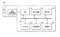
- 1B for example, the lens group 140, the solid-state imaging device 1, the digital signal processor (DSP) 141, the frame memory 142, the display device 143, the recording device 144, the operation system 145, and the power supply system 146. It is comprised including.
- the DSP 141, the frame memory 142, the display device 143, the recording device 144, the operation system 145, and the power supply system 146 are electrically connected by a bus line 147.
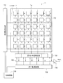
- the solid-state imaging device 1 includes, for example, an imaging region 1a, a vertical drive circuit 131, a column signal processing circuit 133, a horizontal drive circuit 134, an output circuit 136, and a control circuit 130 on a semiconductor substrate (for example, a silicon semiconductor substrate). And have. In the imaging area 1a, a plurality of pixels P including a photoelectric conversion element 10 described later are arranged in a two-dimensional array. Note that circuits such as the vertical drive circuit 131, the column signal processing circuit 133, the horizontal drive circuit 134, the output circuit 136, and the control circuit 130 can be configured from various circuits used in the solid-state imaging device.
- the solid-state imaging device 1 may be a so-called front side irradiation type or a so-called back side irradiation type.
- a shutter device for controlling the incidence of light on the pixel P may be arranged as necessary.
- the vertical drive circuit 131 is constituted by a shift register, for example, and selectively scans each pixel P in the imaging region 1a in the vertical direction sequentially in units of rows.
- a pixel signal (a signal based on a current generated according to the amount of received light) output from each pixel P in the pixel row selectively scanned by the vertical drive circuit 131 is sent to the column signal processing circuit 133 via the vertical signal line 132. It is done.
- the column signal processing circuit 133 is arranged for each pixel column, for example, and is formed for each pixel P in a black reference pixel (for example, a peripheral region of the imaging region 1a) with respect to a signal output from one row of pixels P. For example, signal processing such as noise removal and signal amplification is performed.
- a horizontal selection switch is provided at the output stage of the column signal processing circuit 133, and the column signal processing circuit 133 and the horizontal signal line 135 are connected via the horizontal selection switch.
- the horizontal driving circuit 134 is configured by, for example, a shift register, and sequentially outputs each of the column signal processing circuits 133 by sequentially outputting horizontal scanning pulses, and signals from each of the column signal processing circuits 133 are transmitted to the horizontal signal line 135. Output.
- the output circuit 136 performs signal processing on the signals sequentially supplied from the horizontal signal line 135 and outputs them (generates an output signal Vout).
- the control circuit 130 generates a clock signal and a control signal that serve as a reference for operations of the vertical drive circuit 131, the column signal processing circuit 133, and the horizontal drive circuit 134 based on, for example, a vertical synchronization signal, a horizontal synchronization signal, and a master clock. It is.
- the generated clock signal and control signal are input to the vertical drive circuit 131, the column signal processing circuit 133, and the horizontal drive circuit 134.
- the imaging region 1a has, for example, a plurality of pixels P that are two-dimensionally arranged in a matrix.
- a pixel drive line Lread (specifically, a row selection line and a reset control line) is arranged for each pixel row, and a vertical signal line 132 is arranged for each pixel column.
- the pixel drive line Lread supplies a drive signal for reading a signal from the pixel.
- One end of the pixel drive line Lread is connected to an output end corresponding to each row of the vertical drive circuit 131.
- Each pixel P is formed with a photoelectric conversion element using an organic semiconductor, as will be described in detail later.
- An on-chip lens and a protective film may be provided on the light incident side of the imaging region 1a.
- the color filter may or may not be provided as necessary.
- the photoelectric conversion layer itself can function as a color filter by selecting a photoelectric conversion material. In such a case, color separation is possible without providing a color filter.
- a color filter is disposed on the light incident side of the pixel P, for example, a known color filter that transmits one or more wavelengths of red, green, blue, cyan, magenta, yellow, and the like is used. be able to.
- FIG. 2 schematically shows a main configuration of a photoelectric conversion element (photoelectric conversion element 10) formed in each pixel of the imaging region 1a.
- the photoelectric conversion element 10 includes a first electrode (pixel electrode) 12, a photoelectric conversion layer 13, and a second electrode 14 in this order on a support substrate 11.
- the photoelectric conversion element 10 is configured such that light can be incident from both the first electrode 12 side and the second electrode 14 side (upper and lower) of the photoelectric conversion layer 13.
- the incident direction of light is not particularly limited, and may be configured such that light can be incident only from the first electrode 12 side, or configured such that light can be incident only from the second electrode 14 side. It doesn't matter.
- the support substrate 11 is made of a material such as glass, plastic or silicon.
- the substrate material is not particularly limited, but when light is incident from the first electrode 12 side, a material having transparency in the visible light region is selected.
- the support substrate 11 is formed of a silicon semiconductor substrate, the above-described drive circuit is provided on the silicon semiconductor substrate, and the photoelectric conversion element 10 is mounted on the silicon semiconductor substrate.
- a laminated structure can also be used.
- the first electrode 12 is made of a conductive material such as a transparent conductive film and metal.
- a transparent conductive film having transparency in the visible light region is selected as the constituent material of the first electrode 12.
- the transparent conductive film include indium tin oxide (ITO), indium gallium zinc (IGZO), zinc oxide (ZnO), indium zinc oxide (IZO), iridium dioxide (IrO 2 ), and titanium dioxide (TiO 2 ).
- a transparent conductive film comprising at least one of tin dioxide (SnO 2 ).
- An example of the metal material is aluminum (Al).
- the photoelectric conversion layer 13 includes at least one organic semiconductor. Desirably, it includes different types of materials, specifically, a hole transporting material (donor material) and an electron transporting material (acceptor material). This is because a bulk heterojunction (bulk heterostructure) is formed by mixing the hole transporting material and the electron transporting material, and the photoelectric conversion efficiency can be increased.
- the hole transporting material and the electron transporting material are formed, for example, by being stacked or mixed in the photoelectric conversion layer 13.
- the organic semiconductor various organic pigments can be used.
- subphthalocyanine derivatives for example, subphthalocyanine derivatives, quinacridone derivatives, phthalocyanine derivatives, oxadiazole derivatives, stilbene derivatives, perylene derivatives, tetracyanoquinodimethane derivatives, phenanthroline derivatives. , Naphthalene derivatives, pyrene derivatives, and fluoranthene derivatives.
- a metal complex dye etc. may be used.
- other organic materials such as fullerene (C60) and BCP (Bathocuproine) may be laminated on the photoelectric conversion layer 13.
- the film thickness of this photoelectric converting layer 13 is not specifically limited, For example, they are 50 nm or more and 1 micrometer or less.
- the electron transporting material includes a subphthalocyanine derivative among the materials described above.
- the hole transporting material at this time includes, for example, a quinacridone derivative such as 2,9-di-tert-butylquinacridone or N-methylquinacridone.
- the quantum efficiency of at least one organic semiconductor is 1% or less. More desirably, it is 0.1% or more and 0.7% or less.
- the quantum efficiency here is the quantum efficiency of the organic semiconductor itself (of the organic semiconductor alone) and is the quantum efficiency obtained in the single-layer film of the organic semiconductor.
- R1 to R12 are each, for example, a hydrogen atom (H), a halogen atom (F, Cl, Br, I), a linear, branched or cyclic alkyl group, a phenyl group, a linear or condensed aromatic ring Group, partial fluoroalkyl group, perfluoroalkyl group, halide group, silylalkyl group, silylalkoxy group, arylsilyl group, thioalkyl group, thioaryl group, arylsulfonyl group, alkylsulfonyl group, amino group, alkylamino group, Arylamino group, hydroxy group, alkoxy group, acylamino group, acyloxy group, carboxy group, carboximide group, carboalkoxy group, acyl group, sulfonyl group
- M contains boron (B), a divalent metal, or a trivalent metal.
- X includes an anionic group and any one of the same group of substituents as R1 to R12.
- Z represents nitrogen (N), CH, or hydrogen in CH substituted by any one of the same group of substituents as R1 to R12.
- a subphthalocyanine derivative represented by the following general formulas of Chemical Formula 2, Chemical Formula 3, and Chemical Formula 4 is used. That is, in the general formula of the above chemical formula 1, R1, R4, R5, R8, R9, and R12 are hydrogen atoms, and R2, R3, R6, R7, R10, and R11 are fluorine atoms. Further, in Chemical Formula 2, M is boron, X is fluorine, and Z is nitrogen. In Chemical Formula 3, M is boron, X is phenol substituted with fluorine, and Z is nitrogen. In Chemical Formula 4, M is boron, X is chlorine, and Z is nitrogen.
- the single quantum efficiency of each is low (1% or less), and as described in detail later, free carriers after dissociation of excitons are reduced. It becomes easy to conduct, and as a result, photoresponsiveness can be improved. This is due to the following reason. That is, it is considered that by making R2, R3, R6, R7, R10, and R11 in Chemical Formula 1 a fluorine atom, the intermolecular interaction is weakened, thereby increasing the amorphous nature. In the case of an organic semiconductor having an amorphous property, the energy level is less likely to be confused as compared to those containing many grain boundaries such as polycrystal or microcrystal.
- R1 to R12 in Chemical Formula 1 may be a part of a condensed aliphatic ring or a condensed aromatic ring, and these rings contain one or more atoms other than carbon. Also good. Furthermore, as represented by the general formula of Chemical Formula 5 below, it may contain two or more subphthalocyanine derivatives, or has a structure in which one subphthalocyanine derivative and a subporphyrin ring are bonded. You may do it. R13 is a substituent which can be bonded to one or more subphthalocyanine derivatives or subporphyrin rings via M or any part of R1 to R12 (substituents similar to R1 to R12 above). Any of the group of groups).
- the second electrode 14 is made of a conductive material such as a transparent conductive film and metal.
- a transparent conductive film having transparency in the visible light region is selected as the constituent material of the second electrode 14.
- the transparent conductive film include indium tin oxide (ITO), indium gallium zinc (IGZO), zinc oxide (ZnO), indium zinc oxide (IZO), iridium dioxide (IrO 2 ), and titanium dioxide (TiO 2 ).
- a transparent conductive film comprising at least one of tin dioxide (SnO 2 ).
- An example of the metal material is aluminum (Al).
- FIG. 3 are schematic views for explaining a manufacturing method of the photoelectric conversion element 10 shown in FIG.
- the photoelectric conversion element 10 can be manufactured as follows, for example. That is, first, as shown in FIG. 3, the first electrode 12 made of the above-described material (for example, ITO) is formed on the support substrate 11 made of the above-described material by a sputtering method, for example, with a film thickness of about 100 nm. To do. Thereafter, the first electrode 12 is patterned by etching using, for example, a photolithography method.
- the first electrode 12 made of the above-described material for example, ITO
- a sputtering method for example, with a film thickness of about 100 nm.
- the first electrode 12 is patterned by etching using, for example, a photolithography method.
- the photoelectric conversion layer 13 is formed on the first electrode 12.
- a mixture of a hole transporting material and an electron transporting material as described above, for example, by vapor deposition using a resistance heating type vacuum vapor deposition apparatus is formed on the first electrode 12 with, for example, 100 nm.
- the film is formed with a film thickness.
- the photoelectric conversion layer 13 can be formed by various methods in addition to the resistance heating type vacuum deposition method as described above, depending on the material to be used. Examples thereof include various chemical vapor deposition methods (CVD methods) including coating methods, physical vapor deposition methods (PVD methods), and MOCVD methods. Examples of coating methods include spin coating, dipping, casting, screen printing, inkjet printing, offset printing, gravure printing, stamping, spraying, air doctor coater, blade coater, and rod coater. Method, knife coater method, squeeze coater method, reverse roll coater method, transfer roll coater method, gravure coater method, kiss coater method, cast coater method, spray coater method, slit orifice coater method and calendar coater method.
- CVD methods chemical vapor deposition methods
- PVD methods physical vapor deposition methods
- MOCVD methods MOCVD methods
- coating methods include spin coating, dipping, casting, screen printing, inkjet printing, offset printing, gravure printing, stamping, spraying, air doctor coater, blade coater
- a nonpolar or low polarity organic solvent such as toluene, chloroform, hexane, or ethanol can be used as the solvent.
- a vacuum deposition method electron beam heating method, resistance heating method, flash deposition, etc.
- plasma deposition method sputtering method (bipolar sputtering method, direct current sputtering method, direct current magnetron sputtering method, high frequency sputtering method, magnetron) Sputtering method, ion beam sputtering method, bias sputtering method, etc.), ion plating method (DC (direct current) method, RF method, multi-cathode method, activation reaction method, field evaporation method, high-frequency ion plating method, reactivity) Ion plating method).
- DC direct current
- the second electrode 14 made of the above-described material (for example, Al) is formed on the photoelectric conversion layer 13 with a film thickness of 100 nm by, for example, a vacuum deposition method.
- the photoelectric conversion element 10 which has the photoelectric converting layer 13 which has a bulk heterojunction shown in FIG. 2 can be manufactured.
- the solid-state imaging device 1 of the present embodiment light incident on the imaging region 1a is photoelectrically converted in the photoelectric conversion element 10 of each pixel P. Specifically, the light incident on the photoelectric conversion element 10 passes through the first electrode 12 (or passes through the second electrode 14), for example, and reaches the photoelectric conversion layer 13. In the photoelectric conversion layer 13, pairs of electrons and holes (excitons) are generated, and one of them (for example, electrons) is read to the vertical signal line 132 as a signal charge. The read signal is output to the outside through the horizontal signal line 135. Alternatively, it may be input to the DSP 141 or the like shown in FIG. 1B and held in the recording device 144. In this way, the solid-state imaging device 1 can acquire an electrical signal by photoelectric conversion.
- the photoelectric conversion layer 13 using the organic semiconductor as described above it is desired to improve its photoresponsiveness.
- the organic semiconductor thin film when the quantum efficiency of the organic semiconductor alone is high, the energy level tends to expand in the film. That is, HOMO (Highest Occupied Molecular Orbital) levels or LUMO (Lowest Unoccupied Molecular Orbital) levels are randomly distributed, and exciton dissociation is easily promoted by light absorption.
- the organic semiconductor material itself contained in the photoelectric conversion layer 13 has a low quantum efficiency, specifically, 1% or less, and this makes it difficult to randomly distribute energy levels. Can do. That is, the randomness of the energy level of the organic semiconductor contained in the photoelectric conversion layer affects the quantum efficiency, and in an organic semiconductor having a low quantum efficiency (quantum efficiency of 1% or less), free carriers are easily conducted. This leads to an improvement in photoresponsiveness.
- the photoelectric conversion layer 13 has an electron transporting material and a hole transporting material, and by making the quantum efficiency of the electron transporting material of these materials 1% or less, the photoresponsiveness is effectively improved. Can be made. This is due to the following reason. That is, the photoresponsiveness in the photoelectric conversion element that is generated by pairs of holes and electrons is affected by a carrier type having a low carrier mobility among holes and electrons. Therefore, the responsiveness of the photoelectric conversion element is determined not by the balance between the hole mobility and the electron mobility but by the carrier type having the lower responsiveness. For example, when the photoresponsiveness is easily affected by electron mobility, it is desirable to lower the quantum efficiency of the electron transporting material.
- the quantum efficiency (hereinafter referred to as sensitivity) of the entire photoelectric conversion layer 13 is also an important factor.
- sensitivity the quantum efficiency of the entire photoelectric conversion layer 13
- the photoresponsiveness can be improved as described above, but on the other hand, the organic semiconductor having a low quantum efficiency.
- the sensitivity is lowered.
- the photoelectric conversion layer 13 has a bulk heterojunction made of different materials. Thereby, it is possible to increase the sensitivity of the entire photoelectric conversion layer 13 or to suppress the decrease in sensitivity. This is due to the following reason. That is, in general, in the photoelectric conversion layer 13, excitons generated after light absorption are strongly bound, and free carriers are hardly generated with energy of about room temperature. For this reason, dissociation of excitons can be promoted at the heterointerface by bonding (bulk heterojunction) dissimilar materials (hole transport material and electron transport material) having different energy levels. The energy difference between the molecules constituting the photoelectric conversion layer 13 leads to the promotion of free carrier generation.
- the photoelectric conversion layer 13 includes a bulk heterojunction of an electron transporting material and a hole transporting material, the photoresponsiveness can be improved while increasing the quantum efficiency (sensitivity) of the entire photoelectric conversion layer 13. It is possible to improve two characteristics that are originally in a trade-off relationship.
- the quantum efficiency of the organic semiconductor included in the photoelectric conversion layer 13 is 1% or less, the spread of energy level distribution in the organic semiconductor is suppressed, and free carriers are conducted. It can be made easy. Therefore, it is possible to improve photoresponsiveness.
- Example 1 In the photoelectric conversion element 10 shown in FIG. 2, the response time when the subphthalocyanine derivative shown in Chemical Formula 2 was used as the photoelectric conversion layer 13 was measured.
- a first electrode made of ITO, a photoelectric conversion layer 13, and a second electrode 14 made of Al were formed in this order on a support substrate 11 made of quartz.
- a subphthalocyanine derivative (Chemical Formula 2) was formed to a thickness of 100 nm by a vacuum deposition method.
- the quantum efficiency (%) of the subphthalocyanine derivative (Chemical Formula 2) is ⁇ 5.0 ⁇ 10 5 (V / cm) ( ⁇ 5.0 ⁇ E + 5 (V / cm)) applied to the first electrode 12.
- the light amount when the photocurrent density was 1 ( ⁇ A / cm 2 ) was calculated.
- the response time (s) is excited so that the photocurrent density becomes 1 ( ⁇ A / cm 2 ) when ⁇ 5.0 ⁇ 10 5 (V / cm) is applied to the first electrode 12.
- Light irradiation at a wavelength of 530 nm the time from the end of light irradiation until the photocurrent density attenuates to 0.1 ( ⁇ A / cm 2 ) (that is, the time until the photocurrent attenuates to 10% at the time of light irradiation Time).
- the quantum efficiency of the subphthalocyanine derivative was 0.1%, and the response time was 1.9 ⁇ 10 ⁇ 5 (s).
- Example 1 a device using a subphthalocyanine derivative represented by the following general formula 6 was produced. Furthermore, as a comparative example (comparative example 2) of Example 1, a device using a subphthalocyanine derivative represented by the general formula of Chemical Formula 7 below was produced. In these Comparative Examples 1 and 2 as well, except that the organic semiconductor used for the photoelectric conversion layer was different, an element was produced in the same manner as in Example 1 above, and the quantum efficiency and response time were measured.
- Example 2 In the photoelectric conversion element 10 illustrated in FIG. 2, the response time when the subphthalocyanine derivative represented by Chemical Formula 3 was used as the photoelectric conversion layer 13 was measured. Except that the organic semiconductor used for the photoelectric conversion layer 13 is different, an element was produced in the same manner as in Example 1, and the quantum efficiency and response time were measured.
- the quantum efficiency of the subphthalocyanine derivative was 0.3%, and the response time was 3.0 ⁇ 10 ⁇ 5 (s). Also in Example 2, the response time could be shortened compared to Comparative Examples 1 and 2 above.
- Example 3 In the photoelectric conversion element 10 shown in FIG. 2, the response time when the subphthalocyanine derivative shown in Chemical Formula 4 was used as the photoelectric conversion layer 13 was measured. Except that the organic semiconductor used for the photoelectric conversion layer 13 is different, an element was produced in the same manner as in Example 1, and the quantum efficiency and response time were measured.
- the quantum efficiency of the subphthalocyanine derivative was 0.7%, and the response time was 3.5 ⁇ 10 ⁇ 5 (s). Also in Example 3, the response time could be shortened compared to Comparative Examples 1 and 2 above.
- FIG. 6 shows the response times of Examples 1 to 3 and Comparative Examples 1 and 2.
- Examples 1 to 3 using an organic semiconductor having a quantum efficiency of 1% or less for the photoelectric conversion layer 13 the response time is shorter than those in Comparative Examples 1 and 2 using an organic semiconductor having a quantum efficiency of more than 1%. Recognize.
- the quantum efficiency is 1% or less, which is advantageous for improving the photoresponsiveness.
- Example 4 In the photoelectric conversion element 10 shown in FIG. 2, as the photoelectric conversion layer 13, a bulk heterojunction is formed by mixing an electron transporting material and a hole transporting material. The response time was measured when subphthalocyanine derivatives were used.
- a first electrode made of ITO, a photoelectric conversion layer 13, and a second electrode 14 made of Al were formed in this order on a support substrate 11 made of quartz.
- a subphthalocyanine derivative (Chemical Formula 2) and 2,9-di-tert-butylquinacridon as a hole transporting material are deposited at a deposition rate of 1: 1 to 100 nm by vacuum deposition.
- the response time (s) was measured in the same manner as in Example 1.
- the quantum efficiency of the subphthalocyanine derivative (Chemical Formula 2) is 0.1% as described in Example 1.
- Example 4 Comparative Example 3
- an element using a subphthalocyanine derivative represented by the general formula of Chemical Formula 6 as an electron transporting material was prepared, and other conditions were the same as in Example 4. The response time was measured.
- Example 4 As a result of the above measurement, in Example 4 using the photoelectric conversion layer 13 in which a bulk heterojunction was formed using a subphthalocyanine derivative (chemical formula 2) having a quantum efficiency of 0.1%, the response time was 4.0 ⁇ 10 ⁇ . 5 (s). In Comparative Example 3, it was 3.5 ⁇ 10 ⁇ 4 (s). In Example 4, compared with Comparative Example 3, the response time could be shortened.
- a subphthalocyanine derivative chemical formula 2 having a quantum efficiency of 0.1%
- Example 5 In the photoelectric conversion element 10 illustrated in FIG. 2, as the photoelectric conversion layer 13, an electron transporting material and a hole transporting material are stacked to form a bulk heterojunction. The response time when a subphthalocyanine derivative was used was measured.
- a first electrode made of ITO, a photoelectric conversion layer 13, and a second electrode 14 made of Al were formed in this order on a support substrate 11 made of quartz.
- the first electrode 12 was formed with a thickness of 100 nm by sputtering.
- a subphthalocyanine derivative (Chemical Formula 3) and N-methylquinacridone as a hole transporting material were formed to a thickness of 100 nm by a vacuum deposition method at a deposition rate of 1: 1.
- the response time (s) was measured in the same manner as in Example 1. Further, as described in Example 2, the quantum efficiency of the subphthalocyanine derivative (Chemical Formula 3) is 0.3%.
- Example 5 Comparative Example 4
- an element using a subphthalocyanine derivative represented by the general formula of Chemical Formula 6 as an electron transporting material was prepared, and other conditions were the same as in Example 5. The response time was measured.
- Example 5 As a result of the above measurement, in Example 5 using the photoelectric conversion layer 13 in which a bulk heterojunction was formed using a subphthalocyanine derivative (chemical formula 3) having a quantum efficiency of 0.3%, the response time was 2.0 ⁇ 10 ⁇ . 5 (s). In Comparative Example 4, it was 3.0 ⁇ 10 ⁇ 4 (s). In Example 5, compared with Comparative Example 3, the response time could be shortened.
- a subphthalocyanine derivative chemical formula 3
- Example 6 In the photoelectric conversion element 10 illustrated in FIG. 2, as the photoelectric conversion layer 13, an electron transporting material and a hole transporting material are stacked to form a bulk heterojunction, and the electron transporting material is represented by the above chemical formula 4 The response time when a subphthalocyanine derivative was used was measured.
- a first electrode made of ITO, a photoelectric conversion layer 13, and a second electrode 14 made of Al were formed in this order on a support substrate 11 made of quartz.
- the first electrode 12 was formed with a thickness of 100 nm by sputtering.
- a subphthalocyanine derivative (Chemical Formula 4) and 2,9-di-tert-butylquinacridon as a hole transporting material are deposited at a deposition rate of 1: 1 to 100 nm by vacuum deposition.
- the response time (s) was measured in the same manner as in Example 1. Further, as described in Example 3, the quantum efficiency of the subphthalocyanine derivative (Chemical Formula 4) is 0.7%.
- Example 5 using the photoelectric conversion layer 13 in which a bulk heterojunction was formed using a subphthalocyanine derivative (chemical formula 4) having a quantum efficiency of 0.7%, the response time was 8.3 ⁇ 10 ⁇ . 5 (s). Also in Example 6, the response time could be shortened as compared with Comparative Example 3.
- the solid-state imaging device 1 can be applied to all types of electronic devices having an imaging function, such as a camera system such as a digital still camera and a video camera, and a mobile phone having an imaging function.
- FIG. 7 shows a schematic configuration of the electronic apparatus 2 (camera) as an example.
- the electronic device 2 is, for example, a video camera capable of shooting a still image or a moving image, and drives the solid-state imaging device 1, the optical system (optical lens) 310, the shutter device 311, the solid-state imaging device 1 and the shutter device 311. And a signal processing unit 312.
- the optical system 310 guides image light (incident light) from a subject to the imaging region 1 a of the solid-state imaging device 1.
- the optical system 310 may be composed of a plurality of optical lenses.
- the shutter device 311 controls the light irradiation period and the light shielding period for the solid-state imaging device 1.
- the drive unit 313 controls the transfer operation of the solid-state imaging device 1 and the shutter operation of the shutter device 311.
- the signal processing unit 312 performs various types of signal processing on the signal output from the solid-state imaging device 1.
- the video signal Dout after the signal processing is stored in a storage medium such as a memory, or is output to a monitor or the like.
- the layer structure of the photoelectric conversion element described in the above embodiment is an example, and may further include another layer.
- various intermediate layers such as an electron block layer, a buffer layer, and an active layer may be provided between the photoelectric conversion layer 13 and each electrode.
- the material and thickness of each layer are examples, and are not limited to those described above.
- the present disclosure may be configured as follows. (1) A first electrode; A photoelectric conversion layer including an organic semiconductor provided on the first electrode and having a quantum efficiency of 1% or less; A photoelectric conversion element comprising: a second electrode provided on the photoelectric conversion layer. (2) The photoelectric conversion layer is configured to include a bulk heterojunction of a hole transporting material and an electron transporting material, The photoelectric conversion element according to (1), wherein a quantum efficiency of the electron transporting material in the photoelectric conversion layer is 1% or less. (3) The photoelectric conversion element according to (2), wherein the electron transporting material includes a subphthalocyanine derivative. (4) The said sub phthalocyanine derivative is represented by the general formula of following Chemical formula 1. The photoelectric conversion element as described in said (3).
- R1 to R12 are each a hydrogen atom, a halogen atom (F, Cl, Br, I), a linear, branched or cyclic alkyl group, a phenyl group, a linear or condensed aromatic ring group, or a partial fluoroalkyl group.
- (6) The photoelectric conversion element according to any one of (2) to (5), wherein the quantum efficiency is not less than 0.1% and not more than 0.7%.
- One or both of the first electrode and the second electrode is a transparent oxide semiconductor.
- the transparent oxide semiconductor includes indium tin oxide (ITO), indium gallium zinc (IGZO), zinc oxide (ZnO), indium zinc oxide (IZO), iridium oxide (IrO 2 ), and titanium oxide (TiO 2 ).
- the photoelectric conversion element according to (7) including at least one of tin oxide (SnO 2 ).
- the photoelectric conversion layer including an organic semiconductor having a quantum efficiency of 1% or less on the first electrode; The manufacturing method of the photoelectric conversion element which forms a 2nd electrode on the said photoelectric converting layer.
- the photoelectric conversion layer is configured to include a bulk heterojunction of a hole transporting material and an electron transporting material, The quantum efficiency of the electron transport material in the photoelectric conversion layer is 1% or less.
- the said subphthalocyanine derivative is represented by the general formula of following Chemical formula 1.
- R1 to R12 are each a hydrogen atom, a halogen atom (F, Cl, Br, I), a linear, branched or cyclic alkyl group, a phenyl group, a linear or condensed aromatic ring group, or a partial fluoroalkyl group.
- the quantum efficiency is 0.1% or more and 0.7% or less.
- One or both of the first electrode and the second electrode is a transparent oxide semiconductor.
- the transparent oxide semiconductor includes indium tin oxide (ITO), indium gallium zinc (IGZO), zinc oxide (ZnO), indium zinc oxide (IZO), iridium oxide (IrO 2 ), and titanium oxide (TiO 2 ).
Landscapes
- Chemical & Material Sciences (AREA)
- Physics & Mathematics (AREA)
- Electromagnetism (AREA)
- Inorganic Chemistry (AREA)
- Engineering & Computer Science (AREA)
- Materials Engineering (AREA)
- Light Receiving Elements (AREA)
- Solid State Image Pick-Up Elements (AREA)
Abstract
この光電変換素子は、第1電極と、第1電極上に設けられると共に、量子効率が1%以下である有機半導体を含む光電変換層と、光電変換層上に設けられた第2電極とを備えたものである。
Description
本開示は、例えばCCD(Charge Coupled Device)あるいはCMOS(Complementary Metal Oxide Semiconductor)イメージセンサなどに用いられる光電変換素子、光電変換素子の製造方法および固体撮像装置に関する。
近年、CCDあるいはCMOSイメージセンサ等の固体撮像装置において、有機半導体よりなる光電変換層を有する光電変換素子を用いたものが提案されている(例えば、特許文献1~5参照)。この有機半導体を用いた光電変換素子では、カラーフィルタが不要であり、無機半導体を用いたものに比べて、構造や製造プロセスを簡素化できる。
特許文献1~3に記載された光電変換素子では、基板上に、下部電極と、有機半導体よりなる光電変換層と、上部電極とがこの順に積層されている。尚、光電変換層と、各電極との間に、電子ブロック層、バッファ層および活性層等の各種中間層が設けられることもある。
上記のような有機半導体を用いた光電変換素子では、光電変換層における光応答性が重要である。デジタルカメラなどに用いられる固体撮像素子では、この光応答性が低いと、動く被写体の撮像時や動画の撮影時に残像が生じてしまう。このため、光応答性の改善が望まれている。
特許文献4,5には、有機半導体を光電変換層に用いた固体撮像素子において、応答性を改善する具体的な手法が提案されている。例えば、特許文献4では、光電変換層が、少なくとも1つの有機化合物半導体で構成され、該光電変換層の正孔移動度をh1とし、電子移動度をe1としたとき、0.1<h1/e1<10を満たす素子構造が提案されている。また、特許文献5では、光電変換層が、少なくとも1つの有機化合物半導体で構成され、該光電変換層の正孔移動度をh1とし、電子移動度をe1としたとき、0.1<h1/e1<10を満たしつつ、正孔移動度h1が8.5E-6cm2/Vs以上3.8E-5cm2/Vs以下であって、かつ、電子移動度e1が9.3E-7cm2/Vs以上7.6E-5cm2/Vs以下に制御する手法が提案されている。これらの手法とは異なる、より簡易な手法の実現が望まれている。
光応答性を向上させることが可能な光電変換素子、光電変換素子の製造方法および固体撮像装置を提供することが望ましい。
本開示の一実施の形態の光電変換素子は、第1電極と、第1電極上に設けられると共に、量子効率が1%以下である有機半導体を含む光電変換層と、光電変換層上に設けられた第2電極とを備えたものである。
本開示の一実施の形態の光電変換素子の製造方法は、第1電極上に、量子効率が1%以下である有機半導体を含む光電変換層を形成し、光電変換層上に、第2電極を形成するものである。
本開示の一実施の形態の固体撮像装置は、上記本開示の一実施の形態の光電変換素子を有するものである。
本開示の一実施の形態の光電変換素子および光電変換素子の製造方法ならびに固体撮像装置では、光電変換層に含まれる有機半導体の量子効率が1%以下である。ここで、1つの有機半導体から構成される単層膜の(有機半導体単独の)量子効率が高いと、該単層膜ではエネルギー準位が拡がり易い。即ち、HOMO(Highest Occupied Molecular Orbital)準位あるいはLUMO(Lowest Unoccupied Molecular Orbital)準位が乱雑に分布し、光吸収によって励起子の解離が促進され易い。一方で、励起子解離後の自由キャリアの伝導においては、エネルギー準位が乱雑に分布している場合、キャリア伝導の活性化エネルギーが大きくなり、自由キャリアが伝導しにくい。即ち、光電変換層に含まれる有機半導体のエネルギー準位の乱雑さは量子効率に影響を与え、量子効率が低い(量子効率が1%以下の)有機半導体では、自由キャリアが伝導し易い。
本開示の一実施の形態の光電変換素子および光電変換素子の製造方法ならびに固体撮像装置によれば、光電変換層が、量子効率が1%以下である有機半導体を含むようにしたので、有機半導体において、エネルギー準位の拡がりを抑え、自由キャリアを伝導させ易くすることができる。よって、光応答性を向上させることが可能となる。
尚、上記内容は本開示の一例である。本開示の効果は、上述したものに限らず、他の異なる効果であってもよいし、更に他の効果を含んでいてもよい。
以下、本開示における実施形態について、図面を参照して詳細に説明する。なお、説明する順序は、下記の通りである。
1.実施形態(量子効率が1%以下である有機半導体を含む光電変換層を有する光電変換素子および固体撮像素子の例)
2.実施例(光電変換層にサブフタロシアニン誘導体を用いた実施例)
3.適用例(カメラの例)
1.実施形態(量子効率が1%以下である有機半導体を含む光電変換層を有する光電変換素子および固体撮像素子の例)
2.実施例(光電変換層にサブフタロシアニン誘導体を用いた実施例)
3.適用例(カメラの例)
<実施の形態>
[構成]
図1Aは、本開示の一の実施形態の固体撮像装置(固体撮像装置1)の機能構成を表したものである。図1Bは、固体撮像装置1が搭載される電子機器の構成を表したものである。固体撮像装置1は、例えばCCDまたはCMOSイメージセンサなどである。図1Bに示した電子機器では、例えばレンズ群140、固体撮像装置1、デジタルシグナルプロセッサ(DSP:Digital Signal Processor)141、フレームメモリ142、表示装置143、記録装置144、操作系145および電源系146を含んで構成されている。これらのうち、DSP141、フレームメモリ142、表示装置143、記録装置144、操作系145および電源系146は、バスライン147により電気的に接続されている。
固体撮像装置1は、例えば半導体基板(例えばシリコン半導体基板)上に、撮像領域1aと、垂直駆動回路131と、カラム信号処理回路133と、水平駆動回路134と、出力回路136と、制御回路130とを有している。撮像領域1aには、後述の光電変換素子10を含む複数の画素Pが、2次元アレイ状に配置されている。尚、垂直駆動回路131、カラム信号処理回路133、水平駆動回路134、出力回路136、および制御回路130等の回路は、固体撮像装置において用いられる様々な回路から構成することができる。尚、この固体撮像装置1は、いわゆる表面照射型であってもよいし、いわゆる裏面照射型であってもよい。また、必要に応じて、画素Pへの光の入射を制御するためのシャッター装置が配置されても構わない。
垂直駆動回路131は、例えば、シフトレジスタによって構成され、撮像領域1aの各画素Pを行単位で順次垂直方向に選択走査するものである。垂直駆動回路131によって選択走査された画素行の各画素Pから出力された画素信号(受光量に応じて生成した電流に基づく信号)は、垂直信号線132を介してカラム信号処理回路133に送られる。
カラム信号処理回路133は、例えば、画素列毎に配置されており、1行分の画素Pから出力される信号に対し、画素P毎に黒基準画素(例えば撮像領域1aの周辺領域に形成されている)からの信号を用いて、例えばノイズ除去および信号増幅等の信号処理を行うものである。カラム信号処理回路133の出力段には水平選択スイッチが設けられ、この水平選択スイッチを介して、カラム信号処理回路133と水平信号線135とが接続されている。
水平駆動回路134は、例えばシフトレジスタによって構成され、水平走査パルスを順次出力することによって、カラム信号処理回路133の各々を順次選択し、カラム信号処理回路133の各々から信号を水平信号線135に出力するものである。
出力回路136は、水平信号線135から順次供給される信号に対し、信号処理を施して出力するものである(出力信号Voutを生成するものである)。
制御回路130は、例えば垂直同期信号、水平同期信号およびマスタクロックに基づいて、垂直駆動回路131、カラム信号処理回路133および水平駆動回路134の動作の基準となるクロック信号および制御信号を生成するものである。生成されたクロック信号および制御信号は、垂直駆動回路131、カラム信号処理回路133および水平駆動回路134に入力される。
撮像領域1aは、例えば行列状に2次元配置された複数の画素Pを有している。この画素Pには、例えば画素行ごとに画素駆動線Lread(具体的には行選択線およびリセット制御線など)が配置され、画素列ごとに垂直信号線132が配置されている。画素駆動線Lreadは、画素からの信号読み出しのための駆動信号を供給するものである。画素駆動線Lreadの一端は、垂直駆動回路131の各行に対応した出力端に接続されている。撮像領域1aの詳細構成については後述する。
各画素Pには、詳細は後述するが、有機半導体を用いた光電変換素子が形成されている。撮像領域1aの光入射側には、オンチップレンズおよび保護膜などが設けられていてもよい。また、有機半導体を用いた光電変換素子では、カラーフィルタは、必要に応じて、設けられていてもよいし、設けられていなくともよい。例えば、光電変換材料の選択により、光電変換層自体をカラーフィルタとしても機能させることが可能である。このような場合には、カラーフィルタを配設しなくとも色分離が可能である。あるいは、画素Pの光入射側にカラーフィルタを配置する場合には、例えば赤色、緑色、青色、シアン色、マゼンダ色および黄色等のうちの1または複数の波長を透過させる周知のカラーフィルタを用いることができる。
図2は、撮像領域1aの各画素に形成される光電変換素子(光電変換素子10)の要部構成を模式的に表したものである。光電変換素子10は、支持基板11上に、第1電極(画素電極)12と、光電変換層13と、第2電極14とをこの順に備えたものである。尚、光電変換素子10では、光電変換層13の第1電極12側と第2電極14側との両方(上下の両方)から光が入射可能に構成されている。但し、光の入射方向は特に限定されるものではなく、第1電極12側からのみ光入射が可能な構成であってもよいし、第2電極14側からのみ光入射が可能な構成であっても構わない。
支持基板11は、ガラス、プラスチックまたはシリコンなどの材料から構成されている。基板材料は特に限定されないが、第1電極12側から光を入射させる場合には、可視光領域において透明性を有する材料が選択される。第1電極12側から光を入射させない場合には、支持基板11をシリコン半導体基板から構成し、このシリコン半導体基板に上述した駆動回路等を設けておき、このシリコン半導体基板に光電変換素子10を積層した構造とすることもできる。
第1電極12は、透明導電膜および金属などの導電性を有する材料から構成されている。第1電極12側から光を入射させる場合には、この第1電極12の構成材料は、可視光領域において透明性を有する透明導電膜が選択される。透明導電膜としては、例えば酸化インジウム錫(ITO)、酸化インジウム・ガリウム・亜鉛(IGZO)、酸化亜鉛(ZnO)、酸化インジウム亜鉛(IZO)、二酸化イリジウム(IrO2)、二酸化チタン(TiO2)および二酸化錫(SnO2)のうちの少なくとも1つを含んで構成された透明導電膜が挙げられる。金属材料としては、例えばアルミニウム(Al)が挙げられる。
光電変換層13は、少なくとも1種の有機半導体を含んで構成されている。望ましくは、異種の材料、具体的には正孔輸送性材料(ドナー性材料)と電子輸送性材料(アクセプタ材料)とを含んで構成される。正孔輸送性材料と電子輸送性材料との混合によりバルクヘテロ接合(バルクヘテロ構造)が形成され、光電変換効率を高めることができるためである。正孔輸送性材料と電子輸送性材料とは、例えば光電変換層13において積層または混合して形成されている。有機半導体としては、様々な有機顔料を用いることができるが、一例としては、サブフタロシアニン誘導体、キナクリドン誘導体、フタロシアニン誘導体、オキサジアゾール誘導体、スチルベン誘導体、ペリレン誘導体、テトラシアノキノジメタン誘導体、フェナントロリン誘導体、ナフタレン誘導体、ピレン誘導体、およびフルオランテン誘導体などが挙げられる。また、金属錯体色素などが用いられてもよい。更に、光電変換層13には、顔料以外にも、フラーレン(C60)およびBCP(Bathocuproine)等の他の有機材料が積層されていてもよい。この光電変換層13の膜厚は、特に限定されないが、例えば50nm以上1μm以下である。
電子輸送性材料は、上述した材料のうちサブフタロシアニン誘導体を含むことが望ましい。このときの正孔輸送性材料は、例えば2,9-ジ-tert-ブチルキナクリドン(2,9-di-tert-butylquinacridon)またはN-メチルキナクリドン(N-methylquinacridone)などのキナクリドン誘導体を含む。
この光電変換層13では、少なくとも1種の有機半導体、例えば電子輸送性材料の量子効率が1%以下である。より望ましくは、0.1%以上0.7%以下である。ここでの量子効率は、有機半導体そのものが持つ(有機半導体単独の)量子効率であり、該有機半導体の単層膜において得られる量子効率である。尚、量子効率nは、入射する光子数に対して発生するキャリア数の比であり、以下の式(A)で表すことができる。但し、hをプランク定数、cを真空中の光速度、qを電子電荷、λを波長、Iを電流、Pを光出力とする。
n={(hc)/(qλ)}・(I/P) ………(A)
n={(hc)/(qλ)}・(I/P) ………(A)
電子輸送性材料としては、例えば以下の化1の一般式で表されるサブフタロシアニン誘導体が用いられることが望ましい。但し、R1~R12はそれぞれ、例えば、水素原子(H)、ハロゲン原子(F,Cl,Br,I)、直鎖、分岐または環状のアルキル基、フェニル基、直鎖または縮環をもつ芳香環基、パーシャルフルオロアルキル基、パーフルオロアルキル基、ハロゲン化物の基、シリルアルキル基、シリルアルコキシ基、アリールシリル基、チオアルキル基、チオアリール基、アリールスルホニル基、アルキルスルホニル基、アミノ基、アルキルアミノ基、アリールアミノ基、ヒドロキシ基、アルコキシ基、アシルアミノ基、アシルオキシ基、カルボキシ基、カルボキシイミド基、カルボアルコキシ基、アシル基、スルホニル基、シアノ基、ニトロ基、ビニル基、アリル基、(メタ)アクリル基、グリシジル基、アジリジン環、イソシアネート基、共役ジエンの基、酸無水物の基、酸塩化物の基、カルボニル基、水酸基、アミド基、クロロメチル基、エステル基、ホルミル基、ニトリル基、カルボジイミド基およびオキサゾリン基よりなる群のうちのいずれかを含む。Mは、ホウ素(B)、2価の金属および3価の金属のいずれかを含む。Xは、アニオン性基および上記R1~R12と同様の置換基の群のうちのいずれかを含む。Zは、窒素(N)、CH、またはCHのうちの水素を、上記R1~R12と同様の置換基の群のうちのいずれかで置換したものである。

また、より望ましくは、電子輸送性材料として、以下の化2、化3および化4の一般式で表されるサブフタロシアニン誘導体が用いられる。即ち、上記の化1の一般式において、R1,R4,R5,R8,R9,R12を水素原子とし、R2,R3,R6,R7,R10,R11をフッ素原子としたものである。更に、化2では、Mがホウ素、Xがフッ素、Zが窒素である。化3では、Mがホウ素、Xがフッ素で置換されたフェノール、Zが窒素である。化4では、Mがホウ素、Xが塩素、Zが窒素である。


上記のような化1ないし化4で表されるサブフタロシアニン誘導体では、それぞれの単独の量子効率が低く(1%以下)、これにより、詳細は後述するが、励起子の解離後の自由キャリアが伝導し易くなり、結果として光応答性を向上させることができる。これは、以下の理由による。即ち、化1におけるR2,R3,R6,R7,R10,R11を、フッ素原子とすることにより、分子間相互作用が弱まり、これによってアモルファス性が高まるためと考えられる。アモルファス性をもつ有機半導体では、多結晶あるいは微結晶のように粒界を多く含むものに比べ、エネルギー準位が乱雑になりにくい。
また、上記化1のR1~R12は、縮合脂肪族の環または縮合芳香族の環の一部であってもよいし、それらの環は、炭素以外の1個または複数の原子を含んでいてもよい。更には、以下の化5の一般式で表されるように、2つ以上のサブフタロシアニン誘導体を含んでいてもよいし、または1つのサブフタロシアニン誘導体と、サブポルフィリン環とが結合した構造を有していてもよい。尚、R13は、Mを介して、または、R1~R12のいずれかの部位を介して、1つ以上のサブフタロシアニン誘導体またはサブポルフィリン環と結合可能な置換基(上記R1~R12と同様の置換基の群のうちのいずれか)である。

第2電極14は、透明導電膜および金属などの導電性を有する材料から構成されている。第2電極14側から光を入射させる場合には、この第2電極14の構成材料は、可視光領域において透明性を有する透明導電膜が選択される。透明導電膜としては、例えば酸化インジウム錫(ITO)、酸化インジウム・ガリウム・亜鉛(IGZO)、酸化亜鉛(ZnO)、酸化インジウム亜鉛(IZO)、二酸化イリジウム(IrO2)、二酸化チタン(TiO2)および二酸化錫(SnO2)のうちの少なくとも1つを含んで構成された透明導電膜が挙げられる。金属材料としては、例えばアルミニウム(Al)が挙げられる。尚、この第2電極14側からのみ光を入射させる場合には、支持基板11および第1電極12の材料は特に限定されない。
[製造方法]
図3~図5は、図2に示した光電変換素子10の製造方法について説明するための模式図である。光電変換素子10は、例えば次のようにして製造することができる。即ち、まず図3に示したように、上述した材料からなる支持基板11上に、上述した材料(例えばITO)よりなる第1電極12を、例えばスパッタ法により、100nm程度の膜厚で成膜する。この後、例えばフォトリソグラフィ法を用いたエッチングにより第1電極12をパターニングする。
図3~図5は、図2に示した光電変換素子10の製造方法について説明するための模式図である。光電変換素子10は、例えば次のようにして製造することができる。即ち、まず図3に示したように、上述した材料からなる支持基板11上に、上述した材料(例えばITO)よりなる第1電極12を、例えばスパッタ法により、100nm程度の膜厚で成膜する。この後、例えばフォトリソグラフィ法を用いたエッチングにより第1電極12をパターニングする。
続いて、図4に示したように、第1電極12上に、光電変換層13を形成する。具体的には、例えば抵抗加熱型真空蒸着装置を用いた蒸着によって、例えば上述したような正孔輸送性材料と電子輸送性材料とを混合したものを、第1電極12上に、例えば100nmの膜厚で成膜する。
光電変換層13は、使用する材料にもよるが、上記のような抵抗加熱型の真空蒸着法の他にも、様々な手法で形成することができる。例えば、塗布法、物理的気相成長法(PVD法)、MOCVD法を含む各種の化学的気相成長法(CVD法)を挙げることができる。塗布法としては、例えば、スピンコート法、浸漬法、キャスト法、スクリーン印刷法、インクジェット印刷法、オフセット印刷法、グラビア印刷法、スタンプ法、スプレー法、エアドクタコーター法、ブレードコーター法、ロッドコーター法、ナイフコーター法、スクイズコーター法、リバースロールコーター法、トランスファーロールコーター法、グラビアコーター法、キスコーター法、キャストコーター法、スプレーコーター法、スリットオリフィスコーター法およびカレンダーコーター法が挙げられる。尚、塗布法では、溶媒として、トルエン、クロロホルム、ヘキサン、エタノールといった無極性または極性の低い有機溶媒を用いることができる。また、PVD法として、真空蒸着法(電子ビーム加熱法、抵抗加熱法、フラッシュ蒸着等)、プラズマ蒸着法、スパッタリング法(2極スパッタリング法、直流スパッタリング法、直流マグネトロンスパッタリング法、高周波スパッタリング法、マグネトロンスパッタリング法、イオンビームスパッタリング法、バイアススパッタリング法等)、イオンプレーティング法(DC(direct current)法、RF法、多陰極法、活性化反応法、電界蒸着法、高周波イオンプレーティング法、反応性イオンプレーティング法等)を挙げることができる。
その後、図5に示したように、光電変換層13上に、上述した材料(例えばAl)よりなる第2電極14を、例えば真空蒸着法により、膜厚100nmで形成する。これにより、図2に示したバルクヘテロ接合をもつ光電変換層13を有する光電変換素子10を製造することができる。
[効果]
本実施の形態の固体撮像装置1では、撮像領域1aに入射した光は、各画素Pの光電変換素子10において光電変換される。具体的には、光電変換素子10に入射した光は、例えば第1電極12を透過して(あるいは第2電極14を透過して)、光電変換層13に到達する。光電変換層13では、電子と正孔の対(励起子)が発生し、それらのうちの一方(例えば電子)が、信号電荷として垂直信号線132へ読み出される。読み出された信号は、水平信号線135を通じて外部に出力される。あるいは、図1Bに示したDSP141等に入力され、記録装置144に保持されてもよい。このようにして、固体撮像装置1では、光電変換による電気信号を取得することができる。
本実施の形態の固体撮像装置1では、撮像領域1aに入射した光は、各画素Pの光電変換素子10において光電変換される。具体的には、光電変換素子10に入射した光は、例えば第1電極12を透過して(あるいは第2電極14を透過して)、光電変換層13に到達する。光電変換層13では、電子と正孔の対(励起子)が発生し、それらのうちの一方(例えば電子)が、信号電荷として垂直信号線132へ読み出される。読み出された信号は、水平信号線135を通じて外部に出力される。あるいは、図1Bに示したDSP141等に入力され、記録装置144に保持されてもよい。このようにして、固体撮像装置1では、光電変換による電気信号を取得することができる。
上記のような有機半導体を用いた光電変換層13では、その光応答性の向上が望まれている。ここで、有機半導体薄膜では、その有機半導体単独の量子効率が高いと、該膜中においてエネルギー準位が拡がり易い。即ち、HOMO(Highest Occupied Molecular Orbital)準位あるいはLUMO(Lowest Unoccupied Molecular Orbital)準位が乱雑に分布し、光吸収によって励起子の解離が促進され易い。
一方で、励起子解離後の自由キャリアの伝導においては、エネルギー準位が乱雑に分布していると、キャリア伝導の活性化エネルギーが大きくなり、キャリア伝導を阻害する。したがって、光電変換層13に含まれる有機半導体の材料そのもののもつ量子効率が低いこと、具体的には1%以下であることが望ましく、これにより、エネルギー準位が乱雑に分布しにくくなると考えることができる。即ち、光電変換層に含まれる有機半導体のエネルギー準位の乱雑さは量子効率に影響を与え、量子効率が低い(量子効率が1%以下の)有機半導体では、自由キャリアが伝導し易い。これが、光応答性の向上につながる。
また、光電変換層13が電子輸送性材料と正孔輸送性材料とを有し、これらのうちの電子輸送性材料の量子効率を1%以下とすることで、光応答性を効果的に向上させることができる。これは、次のような理由による。即ち、正孔および電子が対となって発生する光電変換素子における光応答性は、正孔および電子のうちのキャリア移動度が遅いキャリア種に影響を受ける。したがって、光電変換素子の応答性は、正孔移動度と電子移動度とのバランスではなく、応答性の低い方のキャリア種によって決定される。例えば、光応答性が、電子移動度の影響を受け易い場合には、電子輸送性材料の量子効率を低くすることが望ましい。
ところで、光電変換素子10では、上記のような光応答性に加え、光電変換層13全体の量子効率(以下、感度とする)も重要なファクターである。上述のように、励起子解離後の自由キャリアの伝導においては、エネルギー準位が乱雑に分布していると、キャリア伝導の活性化エネルギーが大きくなり、キャリア伝導を阻害する。つまり、光応答性と感度とは、トレードオフの関係にある。
したがって、光電変換層13における有機半導体の量子効率を低くする(1%以下とする)ことで、上述のように光応答性を向上させることができるが、その一方で、量子効率の低い有機半導体を光電変換層13に単独で用いると、感度の低下につながる。
これに対し、本実施の形態では、光電変換層13が異種材料によるバルクヘテロ接合を有している。これにより、光電変換層13全体の感度を高める、あるいは感度の低下を抑制させることが可能である。これは、次のような理由による。即ち、一般に、光電変換層13では、光吸収後に生じる励起子は強く束縛されており、室温程度のエネルギーでは自由キャリアは生成されにくい。このため、エネルギーレベルの異なる異種材料(正孔輸送性材料および電子輸送性材料)を接合(バルクヘテロ接合)させることで、ヘテロ界面において励起子の解離を促進させることができる。光電変換層13を構成する分子間のエネルギー差が、自由キャリアの発生促進につながるのである。また、励起子解離後の正孔はエネルギーレベルの浅い材料のHOMOを伝導し、電子はエネルギーレベルが深い材料のLUMOを伝導する。このように、異種材料をバルクヘテロ接合させても、自由キャリアの伝導に影響を与えにくい(応答性に影響しにくい)。
よって、光電変換層13が電子輸送性材料と正孔輸送性材料とのバルクヘテロ接合を含むことで、光電変換層13全体の量子効率(感度)を高めつつ、光応答性を向上させることできる。本来トレードオフの関係にある2つの特性の向上を実現することが可能となる。
以上説明したように本実施の形態では、光電変換層13に含まれる有機半導体の量子効率が1%以下であることにより、その有機半導体においてエネルギー準位の分布の拡がりを抑え、自由キャリアを伝導させ易くすることができる。よって、光応答性を向上させることが可能となる。
<実施例>
(実施例1)
図2に示した光電変換素子10において、光電変換層13として、上記化2に示したサブフタロシアニン誘導体を用いた場合の応答時間を測定した。測定用の光電変換素子10としては、石英よりなる支持基板11上に、ITOよりなる第1電極と、光電変換層13と、Alよりなる第2電極14とこの順に形成したものを用いた。光電変換層13としては、サブフタロシアニン誘導体(化2)を真空蒸着法により100nm成膜した。また、サブフタロシアニン誘導体(化2)の量子効率(%)は、第1電極12に、-5.0×10⁵(V/cm)(-5.0×E+5(V/cm))を印加した状態で、光電流密度が1(μA/cm2)となるときの光量において算出した。また、応答時間(s)は、第1電極12に、-5.0×105(V/cm)を印加した状態で、光電流密度が1(μA/cm2)となるように、励起波長530nmで光照射を行い、光照射を終了してから光電流密度が0.1(μA/cm2)まで減衰するまでの時間(すなわち光電流が光照射時の10%まで減衰するまでの時間)とした。
上記測定を行った結果、サブフタロシアニン誘導体(化2)の量子効率は0.1%であり、応答時間は1.9×10⁻⁵(s)となった。
また、実施例1の比較例(比較例1)として、以下の化6の一般式で表されるサブフタロシアニン誘導体を用いた素子を作製した。更に、実施例1の比較例(比較例2)として、以下の化7の一般式で表されるサブフタロシアニン誘導体を用いた素子を作製した。尚、これらの比較例1,2においても、光電変換層に用いる有機半導体が異なること以外は、上記実施例1と同様にして素子を作製し、量子効率および応答時間を測定した。


測定の結果、比較例1のサブフタロシアニン誘導体(化6)の量子効率は7%であり、応答時間は4.0×10⁻⁴(s)となった。比較例2のサブフタロシアニン誘導体(化7)の量子効率は44%であり、応答時間は8.0×10⁻⁴(s)となった。このように、実施例1では、比較例1,2に比べ、応答時間を短くすることが出来た。
(実施例2)
図2に示した光電変換素子10において、光電変換層13として、上記化3に示したサブフタロシアニン誘導体を用いた場合の応答時間を測定した。光電変換層13に用いる有機半導体が異なること以外は、上記実施例1と同様にして素子を作製し、量子効率および応答時間を測定した。
図2に示した光電変換素子10において、光電変換層13として、上記化3に示したサブフタロシアニン誘導体を用いた場合の応答時間を測定した。光電変換層13に用いる有機半導体が異なること以外は、上記実施例1と同様にして素子を作製し、量子効率および応答時間を測定した。
上記測定を行った結果、サブフタロシアニン誘導体(化3)の量子効率は0.3%であり、応答時間は3.0×10⁻⁵(s)となった。実施例2においても、上記比較例1,2に比べ応答時間を短くすることが出来た。
(実施例3)
図2に示した光電変換素子10において、光電変換層13として、上記化4に示したサブフタロシアニン誘導体を用いた場合の応答時間を測定した。光電変換層13に用いる有機半導体が異なること以外は、上記実施例1と同様にして素子を作製し、量子効率および応答時間を測定した。
図2に示した光電変換素子10において、光電変換層13として、上記化4に示したサブフタロシアニン誘導体を用いた場合の応答時間を測定した。光電変換層13に用いる有機半導体が異なること以外は、上記実施例1と同様にして素子を作製し、量子効率および応答時間を測定した。
上記測定を行った結果、サブフタロシアニン誘導体(化4)の量子効率は0.7%であり、応答時間は3.5×10⁻⁵(s)となった。実施例3においても、上記比較例1,2に比べ応答時間を短くすることが出来た。
実施例1~3および比較例1,2の応答時間を図6に示す。光電変換層13に量子効率1%以下の有機半導体を用いた実施例1~3では、量子効率が1%よりも大きい有機半導体を用いた比較例1,2に比べ、応答時間が短いことがわかる。また、この結果から、上記化1の一般式で表されるサブフタロシアニン誘導体の中で、特に上記化2~4の一般式で表される構造、即ちR1,R4,R5,R8,R9,R12を水素原子とし、R2,R3,R6,R7,R10,R11をフッ素原子とした構造を持つことで、量子効率が1%以下となり、光応答性の向上に有利であることがわかる。
(実施例4)
図2に示した光電変換素子10において、光電変換層13として、電子輸送性材料と正孔輸送性材料とを混合することによりバルクヘテロ接合を形成し、電子輸送性材料として、上記化2に示したサブフタロシアニン誘導体を用いた場合の応答時間を測定した。測定用の光電変換素子10としては、石英よりなる支持基板11上に、ITOよりなる第1電極と、光電変換層13と、Alよりなる第2電極14とこの順に形成したものを用いた。光電変換層13として、サブフタロシアニン誘導体(化2)と、正孔輸送性材料としての2,9-ジ-tert-ブチルキナクリドン(2,9-di-tert-butylquinacridon)とを、蒸着レート1:1で真空蒸着法により100nm成膜した。尚、応答時間(s)は、上記実施例1と同様にして測定した。また、サブフタロシアニン誘導体(化2)の量子効率は、実施例1で記載したように、0.1%である。
図2に示した光電変換素子10において、光電変換層13として、電子輸送性材料と正孔輸送性材料とを混合することによりバルクヘテロ接合を形成し、電子輸送性材料として、上記化2に示したサブフタロシアニン誘導体を用いた場合の応答時間を測定した。測定用の光電変換素子10としては、石英よりなる支持基板11上に、ITOよりなる第1電極と、光電変換層13と、Alよりなる第2電極14とこの順に形成したものを用いた。光電変換層13として、サブフタロシアニン誘導体(化2)と、正孔輸送性材料としての2,9-ジ-tert-ブチルキナクリドン(2,9-di-tert-butylquinacridon)とを、蒸着レート1:1で真空蒸着法により100nm成膜した。尚、応答時間(s)は、上記実施例1と同様にして測定した。また、サブフタロシアニン誘導体(化2)の量子効率は、実施例1で記載したように、0.1%である。
また、実施例4の比較例(比較例3)として、上記化6の一般式で表されるサブフタロシアニン誘導体を電子輸送性材料として用いた素子を作製し、その他の条件は実施例4と同様にして応答時間を測定した。
上記測定を行った結果、量子効率0.1%のサブフタロシアニン誘導体(化2)を用いてバルクヘテロ接合を形成した光電変換層13を用いた実施例4では、応答時間が4.0×10⁻⁵(s)となった。また、比較例3では、3.5×10⁻⁴(s)となった。実施例4では、比較例3に比べ、応答時間を短くすることができた。
(実施例5)
図2に示した光電変換素子10において、光電変換層13として、電子輸送性材料と正孔輸送性材料とを積層してバルクヘテロ接合を形成し、電子輸送性材料として、上記化3に示したサブフタロシアニン誘導体を用いた場合の応答時間を測定した。測定用の光電変換素子10としては、石英よりなる支持基板11上に、ITOよりなる第1電極と、光電変換層13と、Alよりなる第2電極14とこの順に形成したものを用いた。第1電極12は、スパッタ法により100nmの厚みで形成した。光電変換層13として、サブフタロシアニン誘導体(化3)と、正孔輸送性材料としてのN-メチルキナクリドン(N-methylquinacridone)とを、蒸着レート1:1で真空蒸着法により100nm成膜した。尚、応答時間(s)は、上記実施例1と同様にして測定した。また、サブフタロシアニン誘導体(化3)の量子効率は、実施例2で記載したように、0.3%である。
図2に示した光電変換素子10において、光電変換層13として、電子輸送性材料と正孔輸送性材料とを積層してバルクヘテロ接合を形成し、電子輸送性材料として、上記化3に示したサブフタロシアニン誘導体を用いた場合の応答時間を測定した。測定用の光電変換素子10としては、石英よりなる支持基板11上に、ITOよりなる第1電極と、光電変換層13と、Alよりなる第2電極14とこの順に形成したものを用いた。第1電極12は、スパッタ法により100nmの厚みで形成した。光電変換層13として、サブフタロシアニン誘導体(化3)と、正孔輸送性材料としてのN-メチルキナクリドン(N-methylquinacridone)とを、蒸着レート1:1で真空蒸着法により100nm成膜した。尚、応答時間(s)は、上記実施例1と同様にして測定した。また、サブフタロシアニン誘導体(化3)の量子効率は、実施例2で記載したように、0.3%である。
また、実施例5の比較例(比較例4)として、上記化6の一般式で表されるサブフタロシアニン誘導体を電子輸送性材料として用いた素子を作製し、その他の条件は実施例5と同様にして応答時間を測定した。
上記測定を行った結果、量子効率0.3%のサブフタロシアニン誘導体(化3)を用いてバルクヘテロ接合を形成した光電変換層13を用いた実施例5では、応答時間が2.0×10⁻⁵(s)となった。また、比較例4では、3.0×10⁻⁴(s)となった。実施例5では、比較例3に比べ、応答時間を短くすることができた。
(実施例6)
図2に示した光電変換素子10において、光電変換層13として、電子輸送性材料と正孔輸送性材料とを積層してバルクヘテロ接合を形成し、電子輸送性材料として、上記化4に示したサブフタロシアニン誘導体を用いた場合の応答時間を測定した。測定用の光電変換素子10としては、石英よりなる支持基板11上に、ITOよりなる第1電極と、光電変換層13と、Alよりなる第2電極14とこの順に形成したものを用いた。第1電極12は、スパッタ法により100nmの厚みで形成した。光電変換層13として、サブフタロシアニン誘導体(化4)と、正孔輸送性材料としての2,9-ジ-tert-ブチルキナクリドン(2,9-di-tert-butylquinacridon)とを、蒸着レート1:1で真空蒸着法により100nm成膜した。尚、応答時間(s)は、上記実施例1と同様にして測定した。また、サブフタロシアニン誘導体(化4)の量子効率は、実施例3で記載したように、0.7%である。
図2に示した光電変換素子10において、光電変換層13として、電子輸送性材料と正孔輸送性材料とを積層してバルクヘテロ接合を形成し、電子輸送性材料として、上記化4に示したサブフタロシアニン誘導体を用いた場合の応答時間を測定した。測定用の光電変換素子10としては、石英よりなる支持基板11上に、ITOよりなる第1電極と、光電変換層13と、Alよりなる第2電極14とこの順に形成したものを用いた。第1電極12は、スパッタ法により100nmの厚みで形成した。光電変換層13として、サブフタロシアニン誘導体(化4)と、正孔輸送性材料としての2,9-ジ-tert-ブチルキナクリドン(2,9-di-tert-butylquinacridon)とを、蒸着レート1:1で真空蒸着法により100nm成膜した。尚、応答時間(s)は、上記実施例1と同様にして測定した。また、サブフタロシアニン誘導体(化4)の量子効率は、実施例3で記載したように、0.7%である。
上記測定を行った結果、量子効率0.7%のサブフタロシアニン誘導体(化4)を用いてバルクヘテロ接合を形成した光電変換層13を用いた実施例5では、応答時間が8.3×10⁻⁵(s)となった。実施例6においても、比較例3に比べ、応答時間を短くすることができた。
<適用例>
上記実施の形態の固体撮像装置1は、例えばデジタルスチルカメラやビデオカメラ等のカメラシステムや、撮像機能を有する携帯電話など、撮像機能を備えたあらゆるタイプの電子機器に適用することができる。図7に、その一例として、電子機器2(カメラ)の概略構成を示す。この電子機器2は、例えば静止画または動画を撮影可能なビデオカメラであり、固体撮像装置1と、光学系(光学レンズ)310と、シャッタ装置311と、固体撮像装置1およびシャッタ装置311を駆動する駆動部313と、信号処理部312とを有する。
上記実施の形態の固体撮像装置1は、例えばデジタルスチルカメラやビデオカメラ等のカメラシステムや、撮像機能を有する携帯電話など、撮像機能を備えたあらゆるタイプの電子機器に適用することができる。図7に、その一例として、電子機器2(カメラ)の概略構成を示す。この電子機器2は、例えば静止画または動画を撮影可能なビデオカメラであり、固体撮像装置1と、光学系(光学レンズ)310と、シャッタ装置311と、固体撮像装置1およびシャッタ装置311を駆動する駆動部313と、信号処理部312とを有する。
光学系310は、被写体からの像光(入射光)を固体撮像装置1の撮像領域1aへ導くものである。この光学系310は、複数の光学レンズから構成されていてもよい。シャッタ装置311は、固体撮像装置1への光照射期間および遮光期間を制御するものである。駆動部313は、固体撮像装置1の転送動作およびシャッタ装置311のシャッタ動作を制御するものである。信号処理部312は、固体撮像装置1から出力された信号に対し、各種の信号処理を行うものである。信号処理後の映像信号Doutは、メモリーなどの記憶媒体に記憶されるか、あるいは、モニタ等に出力される。
以上、実施の形態を挙げて説明したが、本開示内容は上記実施の形態等に限定されるものではなく、種々変形が可能である。例えば、上記実施の形態において説明した光電変換素子の層構成は一例であり、更に他の層を備えていてもよい。例えば、光電変換層13と、各電極との間に、電子ブロック層、バッファ層および活性層等の各種中間層が設けられていてもよい。また、各層の材料や厚みも一例であって、上述のものに限定されるものではない。
また、上記実施の形態等において説明した効果は一例であり、他の効果であってもよいし、更に他の効果を含んでいてもよい。
尚、本開示は、以下のような構成であってもよい。
(1)
第1電極と、
前記第1電極上に設けられると共に、量子効率が1%以下である有機半導体を含む光電変換層と、
前記光電変換層上に設けられた第2電極と
を備えた
光電変換素子。
(2)
前記光電変換層は、正孔輸送性材料と電子輸送性材料とのバルクヘテロ接合を含んで構成され、
前記光電変換層における前記電子輸送性材料の量子効率が1%以下である
上記(1)に記載の光電変換素子。
(3)
前記電子輸送性材料はサブフタロシアニン誘導体を含む
上記(2)に記載の光電変換素子。
(4)
前記サブフタロシアニン誘導体は、以下の化1の一般式で表されるものである
上記(3)に記載の光電変換素子。
(R1~R12はそれぞれ、水素原子、ハロゲン原子(F,Cl,Br,I)、直鎖、分岐または環状のアルキル基、フェニル基、直鎖または縮環をもつ芳香環基、パーシャルフルオロアルキル基、パーフルオロアルキル基、ハロゲン化物の基、シリルアルキル基、シリルアルコキシ基、アリールシリル基、チオアルキル基、チオアリール基、アリールスルホニル基、アルキルスルホニル基、アミノ基、アルキルアミノ基、アリールアミノ基、ヒドロキシ基、アルコキシ基、アシルアミノ基、アシルオキシ基、カルボキシ基、カルボキシイミド基、カルボアルコキシ基、アシル基、スルホニル基、シアノ基、ニトロ基、ビニル基、アリル基、(メタ)アクリル基、グリシジル基、アジリジン環、イソシアネート基、共役ジエンの基、酸無水物の基、酸塩化物の基、カルボニル基、水酸基、アミド基、クロロメチル基、エステル基、ホルミル基、ニトリル基、カルボジイミド基およびオキサゾリン基よりなる群のうちのいずれかを含む。Mは、ホウ素、2価の金属および3価の金属のいずれかを含む。Xは、アニオン性基および上記R1~R12と同様の置換基の群のうちのいずれかを含む。Zは、N、CH、またはCHのうちの水素を、上記R1~R12と同様の置換基の群のうちのいずれかで置換したものである。)

(5)
前記一般式において、R1,R4,R5,R8,R9,R12は水素原子であり、R2,R3,R6,R7,R10,R11はフッ素原子である
上記(4)に記載の光電変換素子。
(6)
前記量子効率は、0.1%以上0.7%以下である
上記(2)~(5)のいずれか1つに記載の光電変換素子。
(7)
前記第1電極および前記第2電極のうちの一方または両方は、透明酸化物半導体である
上記(1)~(6)のいずれか1つに記載の光電変換素子。
(8)
前記透明酸化物半導体は、酸化インジウム錫(ITO)、酸化インジウム・ガリウム・亜鉛(IGZO)、酸化亜鉛(ZnO)、酸化インジウム亜鉛(IZO)、酸化イリジウム(IrO2)、酸化チタン(TiO2)および酸化錫(SnO2)のうちの少なくとも1つを含んで構成されている
上記(7)に記載の光電変換素子。
(9)
第1電極上に、量子効率が1%以下である有機半導体を含む光電変換層を形成し、
前記光電変換層上に、第2電極を形成する
光電変換素子の製造方法。
(10)
前記光電変換層は、正孔輸送性材料と電子輸送性材料とのバルクヘテロ接合を含んで構成され、
前記光電変換層における前記電子輸送性材料の量子効率が1%以下である
上記(9)に記載の光電変換素子の製造方法。
(11)
前記電子輸送性材料はサブフタロシアニン誘導体を含む
上記(10)に記載の光電変換素子の製造方法。
(12)
前記サブフタロシアニン誘導体は、以下の化1の一般式で表されるものである 上記(11)に記載の光電変換素子の製造方法。
(R1~R12はそれぞれ、水素原子、ハロゲン原子(F,Cl,Br,I)、直鎖、分岐または環状のアルキル基、フェニル基、直鎖または縮環をもつ芳香環基、パーシャルフルオロアルキル基、パーフルオロアルキル基、ハロゲン化物の基、シリルアルキル基、シリルアルコキシ基、アリールシリル基、チオアルキル基、チオアリール基、アリールスルホニル基、アルキルスルホニル基、アミノ基、アルキルアミノ基、アリールアミノ基、ヒドロキシ基、アルコキシ基、アシルアミノ基、アシルオキシ基、カルボキシ基、カルボキシイミド基、カルボアルコキシ基、アシル基、スルホニル基、シアノ基、ニトロ基、ビニル基、アリル基、(メタ)アクリル基、グリシジル基、アジリジン環、イソシアネート基、共役ジエンの基、酸無水物の基、酸塩化物の基、カルボニル基、水酸基、アミド基、クロロメチル基、エステル基、ホルミル基、ニトリル基、カルボジイミド基およびオキサゾリン基よりなる群のうちのいずれかを含む。Mは、ホウ素、2価の金属および3価の金属のいずれかを含む。Xは、アニオン性基および上記R1~R12と同様の置換基の群のうちのいずれかを含む。Zは、N、CH、またはCHのうちの水素を、上記R1~R12と同様の置換基の群のうちのいずれかで置換したものである。)

(13)
前記一般式において、R1,R4,R5,R8,R9,R12は水素原子であり、R2,R3,R6,R7,R10,R11はフッ素原子である
上記(12)に記載の光電変換素子の製造方法。
(14)
前記量子効率は、0.1%以上0.7%以下である
上記(10)~(13)のいずれか1つに記載の光電変換素子の製造方法。
(15)
前記第1電極および前記第2電極のうちの一方または両方は、透明酸化物半導体である
上記(9)~(14)のいずれか1つに記載の光電変換素子の製造方法。
(16)
前記透明酸化物半導体は、酸化インジウム錫(ITO)、酸化インジウム・ガリウム・亜鉛(IGZO)、酸化亜鉛(ZnO)、酸化インジウム亜鉛(IZO)、酸化イリジウム(IrO2)、酸化チタン(TiO2)および酸化錫(SnO2)のうちの少なくとも1つを含んで構成されている
上記(9)~(15)のいずれか1つに記載の光電変換素子の製造方法。
(17)
第1電極と、
前記第1電極上に設けられると共に、量子効率が1%以下である有機半導体を含む光電変換層と、
前記光電変換層上に設けられた第2電極と
を備えた
光電変換素子を有する固体撮像装置。
(1)
第1電極と、
前記第1電極上に設けられると共に、量子効率が1%以下である有機半導体を含む光電変換層と、
前記光電変換層上に設けられた第2電極と
を備えた
光電変換素子。
(2)
前記光電変換層は、正孔輸送性材料と電子輸送性材料とのバルクヘテロ接合を含んで構成され、
前記光電変換層における前記電子輸送性材料の量子効率が1%以下である
上記(1)に記載の光電変換素子。
(3)
前記電子輸送性材料はサブフタロシアニン誘導体を含む
上記(2)に記載の光電変換素子。
(4)
前記サブフタロシアニン誘導体は、以下の化1の一般式で表されるものである
上記(3)に記載の光電変換素子。
(R1~R12はそれぞれ、水素原子、ハロゲン原子(F,Cl,Br,I)、直鎖、分岐または環状のアルキル基、フェニル基、直鎖または縮環をもつ芳香環基、パーシャルフルオロアルキル基、パーフルオロアルキル基、ハロゲン化物の基、シリルアルキル基、シリルアルコキシ基、アリールシリル基、チオアルキル基、チオアリール基、アリールスルホニル基、アルキルスルホニル基、アミノ基、アルキルアミノ基、アリールアミノ基、ヒドロキシ基、アルコキシ基、アシルアミノ基、アシルオキシ基、カルボキシ基、カルボキシイミド基、カルボアルコキシ基、アシル基、スルホニル基、シアノ基、ニトロ基、ビニル基、アリル基、(メタ)アクリル基、グリシジル基、アジリジン環、イソシアネート基、共役ジエンの基、酸無水物の基、酸塩化物の基、カルボニル基、水酸基、アミド基、クロロメチル基、エステル基、ホルミル基、ニトリル基、カルボジイミド基およびオキサゾリン基よりなる群のうちのいずれかを含む。Mは、ホウ素、2価の金属および3価の金属のいずれかを含む。Xは、アニオン性基および上記R1~R12と同様の置換基の群のうちのいずれかを含む。Zは、N、CH、またはCHのうちの水素を、上記R1~R12と同様の置換基の群のうちのいずれかで置換したものである。)
前記一般式において、R1,R4,R5,R8,R9,R12は水素原子であり、R2,R3,R6,R7,R10,R11はフッ素原子である
上記(4)に記載の光電変換素子。
(6)
前記量子効率は、0.1%以上0.7%以下である
上記(2)~(5)のいずれか1つに記載の光電変換素子。
(7)
前記第1電極および前記第2電極のうちの一方または両方は、透明酸化物半導体である
上記(1)~(6)のいずれか1つに記載の光電変換素子。
(8)
前記透明酸化物半導体は、酸化インジウム錫(ITO)、酸化インジウム・ガリウム・亜鉛(IGZO)、酸化亜鉛(ZnO)、酸化インジウム亜鉛(IZO)、酸化イリジウム(IrO2)、酸化チタン(TiO2)および酸化錫(SnO2)のうちの少なくとも1つを含んで構成されている
上記(7)に記載の光電変換素子。
(9)
第1電極上に、量子効率が1%以下である有機半導体を含む光電変換層を形成し、
前記光電変換層上に、第2電極を形成する
光電変換素子の製造方法。
(10)
前記光電変換層は、正孔輸送性材料と電子輸送性材料とのバルクヘテロ接合を含んで構成され、
前記光電変換層における前記電子輸送性材料の量子効率が1%以下である
上記(9)に記載の光電変換素子の製造方法。
(11)
前記電子輸送性材料はサブフタロシアニン誘導体を含む
上記(10)に記載の光電変換素子の製造方法。
(12)
前記サブフタロシアニン誘導体は、以下の化1の一般式で表されるものである 上記(11)に記載の光電変換素子の製造方法。
(R1~R12はそれぞれ、水素原子、ハロゲン原子(F,Cl,Br,I)、直鎖、分岐または環状のアルキル基、フェニル基、直鎖または縮環をもつ芳香環基、パーシャルフルオロアルキル基、パーフルオロアルキル基、ハロゲン化物の基、シリルアルキル基、シリルアルコキシ基、アリールシリル基、チオアルキル基、チオアリール基、アリールスルホニル基、アルキルスルホニル基、アミノ基、アルキルアミノ基、アリールアミノ基、ヒドロキシ基、アルコキシ基、アシルアミノ基、アシルオキシ基、カルボキシ基、カルボキシイミド基、カルボアルコキシ基、アシル基、スルホニル基、シアノ基、ニトロ基、ビニル基、アリル基、(メタ)アクリル基、グリシジル基、アジリジン環、イソシアネート基、共役ジエンの基、酸無水物の基、酸塩化物の基、カルボニル基、水酸基、アミド基、クロロメチル基、エステル基、ホルミル基、ニトリル基、カルボジイミド基およびオキサゾリン基よりなる群のうちのいずれかを含む。Mは、ホウ素、2価の金属および3価の金属のいずれかを含む。Xは、アニオン性基および上記R1~R12と同様の置換基の群のうちのいずれかを含む。Zは、N、CH、またはCHのうちの水素を、上記R1~R12と同様の置換基の群のうちのいずれかで置換したものである。)
前記一般式において、R1,R4,R5,R8,R9,R12は水素原子であり、R2,R3,R6,R7,R10,R11はフッ素原子である
上記(12)に記載の光電変換素子の製造方法。
(14)
前記量子効率は、0.1%以上0.7%以下である
上記(10)~(13)のいずれか1つに記載の光電変換素子の製造方法。
(15)
前記第1電極および前記第2電極のうちの一方または両方は、透明酸化物半導体である
上記(9)~(14)のいずれか1つに記載の光電変換素子の製造方法。
(16)
前記透明酸化物半導体は、酸化インジウム錫(ITO)、酸化インジウム・ガリウム・亜鉛(IGZO)、酸化亜鉛(ZnO)、酸化インジウム亜鉛(IZO)、酸化イリジウム(IrO2)、酸化チタン(TiO2)および酸化錫(SnO2)のうちの少なくとも1つを含んで構成されている
上記(9)~(15)のいずれか1つに記載の光電変換素子の製造方法。
(17)
第1電極と、
前記第1電極上に設けられると共に、量子効率が1%以下である有機半導体を含む光電変換層と、
前記光電変換層上に設けられた第2電極と
を備えた
光電変換素子を有する固体撮像装置。
本出願は、日本国特許庁において2015年6月11日に出願された日本特許出願番号第2015-118105号を基礎として優先権を主張するものであり、この出願のすべての内容を参照によって本出願に援用する。
当業者であれば、設計上の要件や他の要因に応じて、種々の修正、コンビネーション、サブコンビネーション、および変更を想到し得るが、それらは添付の請求の範囲やその均等物の範囲に含まれるものであることが理解される。
Claims (17)
- 第1電極と、
前記第1電極上に設けられると共に、量子効率が1%以下である有機半導体を含む光電変換層と、
前記光電変換層上に設けられた第2電極と
を備えた
光電変換素子。 - 前記光電変換層は、正孔輸送性材料と電子輸送性材料とのバルクヘテロ接合を含んで構成され、
前記光電変換層における前記電子輸送性材料の量子効率が1%以下である
請求項1に記載の光電変換素子。 - 前記電子輸送性材料はサブフタロシアニン誘導体を含む
請求項2に記載の光電変換素子。 - 前記サブフタロシアニン誘導体は、以下の化1の一般式で表されるものである
請求項3に記載の光電変換素子。
(R1~R12はそれぞれ、水素原子、ハロゲン原子(F,Cl,Br,I)、直鎖、分岐または環状のアルキル基、フェニル基、直鎖または縮環をもつ芳香環基、パーシャルフルオロアルキル基、パーフルオロアルキル基、ハロゲン化物の基、シリルアルキル基、シリルアルコキシ基、アリールシリル基、チオアルキル基、チオアリール基、アリールスルホニル基、アルキルスルホニル基、アミノ基、アルキルアミノ基、アリールアミノ基、ヒドロキシ基、アルコキシ基、アシルアミノ基、アシルオキシ基、カルボキシ基、カルボキシイミド基、カルボアルコキシ基、アシル基、スルホニル基、シアノ基、ニトロ基、ビニル基、アリル基、(メタ)アクリル基、グリシジル基、アジリジン環、イソシアネート基、共役ジエンの基、酸無水物の基、酸塩化物の基、カルボニル基、水酸基、アミド基、クロロメチル基、エステル基、ホルミル基、ニトリル基、カルボジイミド基およびオキサゾリン基よりなる群のうちのいずれかを含む。Mは、ホウ素、2価の金属および3価の金属のいずれかを含む。Xは、アニオン性基および上記R1~R12と同様の置換基の群のうちのいずれかを含む。Zは、N、CH、またはCHのうちの水素を、上記R1~R12と同様の置換基の群のうちのいずれかで置換したものである。)

- 前記一般式において、R1,R4,R5,R8,R9,R12は水素原子であり、R2,R3,R6,R7,R10,R11はフッ素原子である
請求項4に記載の光電変換素子。 - 前記量子効率は、0.1%以上0.7%以下である
請求項2に記載の光電変換素子。 - 前記第1電極および前記第2電極のうちの一方または両方は、透明酸化物半導体である
請求項1に記載の光電変換素子。 - 前記透明酸化物半導体は、酸化インジウム錫(ITO)、酸化インジウム・ガリウム・亜鉛(IGZO)、酸化亜鉛(ZnO)、酸化インジウム亜鉛(IZO)、酸化イリジウム(IrO2)、酸化チタン(TiO2)および酸化錫(SnO2)のうちの少なくとも1つを含んで構成されている
請求項7に記載の光電変換素子。 - 第1電極上に、量子効率が1%以下である有機半導体を含む光電変換層を形成し、
前記光電変換層上に、第2電極を形成する
光電変換素子の製造方法。 - 前記光電変換層は、正孔輸送性材料と電子輸送性材料とのバルクヘテロ接合を含んで構成され、
前記光電変換層における前記電子輸送性材料の量子効率が1%以下である
請求項9に記載の光電変換素子の製造方法。 - 前記電子輸送性材料はサブフタロシアニン誘導体を含む
請求項10に記載の光電変換素子の製造方法。 - 前記サブフタロシアニン誘導体は、以下の化1の一般式で表されるものである
請求項11に記載の光電変換素子の製造方法。
(R1~R12はそれぞれ、水素原子、ハロゲン原子(F,Cl,Br,I)、直鎖、分岐または環状のアルキル基、フェニル基、直鎖または縮環をもつ芳香環基、パーシャルフルオロアルキル基、パーフルオロアルキル基、ハロゲン化物の基、シリルアルキル基、シリルアルコキシ基、アリールシリル基、チオアルキル基、チオアリール基、アリールスルホニル基、アルキルスルホニル基、アミノ基、アルキルアミノ基、アリールアミノ基、ヒドロキシ基、アルコキシ基、アシルアミノ基、アシルオキシ基、カルボキシ基、カルボキシイミド基、カルボアルコキシ基、アシル基、スルホニル基、シアノ基、ニトロ基、ビニル基、アリル基、(メタ)アクリル基、グリシジル基、アジリジン環、イソシアネート基、共役ジエンの基、酸無水物の基、酸塩化物の基、カルボニル基、水酸基、アミド基、クロロメチル基、エステル基、ホルミル基、ニトリル基、カルボジイミド基およびオキサゾリン基よりなる群のうちのいずれかを含む。Mは、ホウ素、2価の金属および3価の金属のいずれかを含む。Xは、アニオン性基および上記R1~R12と同様の置換基の群のうちのいずれかを含む。Zは、N、CH、またはCHのうちの水素を、上記R1~R12と同様の置換基の群のうちのいずれかで置換したものである。)

- 前記一般式において、R1,R4,R5,R8,R9,R12は水素原子であり、R2,R3,R6,R7,R10,R11はフッ素原子である
請求項12に記載の光電変換素子の製造方法。 - 前記量子効率は、0.1%以上0.7%以下である
請求項10に記載の光電変換素子の製造方法。 - 前記第1電極および前記第2電極のうちの一方または両方は、透明酸化物半導体である
請求項9に記載の光電変換素子の製造方法。 - 前記透明酸化物半導体は、酸化インジウム錫(ITO)、酸化インジウム・ガリウム・亜鉛(IGZO)、酸化亜鉛(ZnO)、酸化インジウム亜鉛(IZO)、酸化イリジウム(IrO2)、酸化チタン(TiO2)および酸化錫(SnO2)のうちの少なくとも1つを含んで構成されている
請求項15に記載の光電変換素子の製造方法。 - 第1電極と、
前記第1電極上に設けられると共に、量子効率が1%以下である有機半導体を含む光電変換層と、
前記光電変換層上に設けられた第2電極と
を備えた
光電変換素子を有する固体撮像装置。
Priority Applications (1)
| Application Number | Priority Date | Filing Date | Title |
|---|---|---|---|
| US15/578,542 US10516124B2 (en) | 2015-06-11 | 2016-06-01 | Photoelectric conversion elements, method of manufacturing photoelectric conversion element, and solid-state imaging device |
Applications Claiming Priority (2)
| Application Number | Priority Date | Filing Date | Title |
|---|---|---|---|
| JP2015-118105 | 2015-06-11 | ||
| JP2015118105 | 2015-06-11 |
Publications (1)
| Publication Number | Publication Date |
|---|---|
| WO2016199632A1 true WO2016199632A1 (ja) | 2016-12-15 |
Family
ID=57504003
Family Applications (1)
| Application Number | Title | Priority Date | Filing Date |
|---|---|---|---|
| PCT/JP2016/066147 WO2016199632A1 (ja) | 2015-06-11 | 2016-06-01 | 光電変換素子、光電変換素子の製造方法および固体撮像装置 |
Country Status (2)
| Country | Link |
|---|---|
| US (1) | US10516124B2 (ja) |
| WO (1) | WO2016199632A1 (ja) |
Cited By (1)
| Publication number | Priority date | Publication date | Assignee | Title |
|---|---|---|---|---|
| JP2022130539A (ja) * | 2016-07-20 | 2022-09-06 | ソニーグループ株式会社 | 固体撮像素子および固体撮像装置 |
Families Citing this family (3)
| Publication number | Priority date | Publication date | Assignee | Title |
|---|---|---|---|---|
| US11296296B2 (en) | 2019-11-06 | 2022-04-05 | Applied Materials, Inc. | Organic light-emtting diode light extraction layer having graded index of refraction |
| US11121345B2 (en) | 2019-11-26 | 2021-09-14 | Applied Materials, Inc. | Structures and methods of OLED display fabrication suited for deposition of light enhancing layer |
| KR20220129601A (ko) | 2020-01-22 | 2022-09-23 | 어플라이드 머티어리얼스, 인코포레이티드 | 미러를 갖는 oled(organic light-emitting diode) 디스플레이 디바이스들 및 이를 제조하기 위한 방법 |
Citations (2)
| Publication number | Priority date | Publication date | Assignee | Title |
|---|---|---|---|---|
| JP2009538529A (ja) * | 2006-05-25 | 2009-11-05 | ザ、トラスティーズ オブ プリンストン ユニバーシティ | サブフタロシアニン化合物を用いた有機感光性デバイス |
| JP2010212455A (ja) * | 2009-03-10 | 2010-09-24 | Nippon Hoso Kyokai <Nhk> | 有機光電変換膜及びこれを含む電子素子 |
Family Cites Families (9)
| Publication number | Priority date | Publication date | Assignee | Title |
|---|---|---|---|---|
| JP4579502B2 (ja) * | 2003-05-02 | 2010-11-10 | キヤノン株式会社 | 構造体及びその製造方法、該構造体を含むトナー並びにそれを用いた画像形成方法及び装置 |
| JP5216373B2 (ja) | 2008-03-06 | 2013-06-19 | 富士フイルム株式会社 | 固体撮像素子 |
| EP2292586B1 (en) * | 2009-09-08 | 2018-01-17 | Fujifilm Corporation | Photoelectric conversion material, film containing the material, photoelectric conversion device, production method thereof, photosensor, imaging device and their use methods |
| JP2012077064A (ja) * | 2010-09-08 | 2012-04-19 | Fujifilm Corp | 光電変換材料、該材料を含む膜、光電変換素子、光電変換素子の製造方法、光電変換素子の使用方法、光センサ、撮像素子 |
| JP5337887B2 (ja) | 2012-01-27 | 2013-11-06 | 富士フイルム株式会社 | 固体撮像素子 |
| JP2013219190A (ja) | 2012-04-09 | 2013-10-24 | Kuraray Co Ltd | 有機光電変換素子 |
| JP2014063999A (ja) | 2012-08-31 | 2014-04-10 | Mitsubishi Chemicals Corp | 有機光電変換素子の製造方法 |
| JP5824436B2 (ja) | 2012-09-28 | 2015-11-25 | 富士フイルム株式会社 | 光電変換素子及びそれを用いた撮像素子 |
| CN106463564A (zh) * | 2014-07-31 | 2017-02-22 | 富士胶片株式会社 | 光电转换元件及成像元件 |
-
2016
- 2016-06-01 US US15/578,542 patent/US10516124B2/en active Active
- 2016-06-01 WO PCT/JP2016/066147 patent/WO2016199632A1/ja active Application Filing
Patent Citations (2)
| Publication number | Priority date | Publication date | Assignee | Title |
|---|---|---|---|---|
| JP2009538529A (ja) * | 2006-05-25 | 2009-11-05 | ザ、トラスティーズ オブ プリンストン ユニバーシティ | サブフタロシアニン化合物を用いた有機感光性デバイス |
| JP2010212455A (ja) * | 2009-03-10 | 2010-09-24 | Nippon Hoso Kyokai <Nhk> | 有機光電変換膜及びこれを含む電子素子 |
Non-Patent Citations (3)
| Title |
|---|
| H. GOMMANS ET AL.: "Perfluorinated Subphthalocyanine as a New Acceptor Material in a Small-Molecule Bilayer Organic Solar Cell", ADVANCED FUNCTIONAL MATERIALS, vol. 19, no. 21, 18 September 2009 (2009-09-18), pages 3435 - 3439, XP001549701 * |
| KWANG-HEE LEE ET AL.: "Green-Sensitive Organic Photodetectors with High Sensitivity and Spectral Selectivity Using Subphthalocyanine Derivatives", ACS APPLIED MATERIALS & INTERFACES, vol. 5, no. 24, 25 November 2013 (2013-11-25), pages 13089 - 13095, XP055200549 * |
| P. SULLIVAN ET AL.: "Halogenated Boron Subphthalocyanines as Light Harvesting Electron Acceptors in Organic Photovoltaics", ADVANCED ENERGY MATERIALS, vol. 1, no. 3, 30 March 2011 (2011-03-30), pages 352 - 355, XP055139770 * |
Cited By (3)
| Publication number | Priority date | Publication date | Assignee | Title |
|---|---|---|---|---|
| JP2022130539A (ja) * | 2016-07-20 | 2022-09-06 | ソニーグループ株式会社 | 固体撮像素子および固体撮像装置 |
| US11730004B2 (en) | 2016-07-20 | 2023-08-15 | Sony Group Corporation | Solid-state imaging element and solid-state imaging apparatus |
| JP7367128B2 (ja) | 2016-07-20 | 2023-10-23 | ソニーグループ株式会社 | 固体撮像素子および固体撮像装置 |
Also Published As
| Publication number | Publication date |
|---|---|
| US10516124B2 (en) | 2019-12-24 |
| US20180269414A1 (en) | 2018-09-20 |
Similar Documents
| Publication | Publication Date | Title |
|---|---|---|
| JP5323025B2 (ja) | 固体撮像素子 | |
| KR101583581B1 (ko) | 광전 변환 소자 및 촬상 소자 | |
| JP6965967B2 (ja) | 撮像素子、積層型撮像素子及び撮像装置 | |
| JP6046649B2 (ja) | 光電変換素子及びそれを用いた撮像素子 | |
| KR101873665B1 (ko) | 광전 변환 소자, 광 센서 및 촬상 소자 | |
| JP6754156B2 (ja) | 固体撮像素子および固体撮像素子の製造方法、光電変換素子、撮像装置、電子機器、並びに光電変換素子。 | |
| WO2016199632A1 (ja) | 光電変換素子、光電変換素子の製造方法および固体撮像装置 | |
| KR101719089B1 (ko) | 광전 변환 소자 및 그 사용 방법, 광 센서, 촬상 소자 | |
| TW201143182A (en) | Photoelectric conversion device, imaging device and production methods thereof | |
| JP5814293B2 (ja) | 光電変換素子および撮像素子、ならびに、光電変換素子の製造方法および撮像素子の製造方法 | |
| CN103811517A (zh) | 光电转换元件、固体摄像装置以及电子设备 | |
| KR101777534B1 (ko) | 광전 변환 소자, 촬상 소자, 광 센서 | |
| JP2018098438A (ja) | 光電変換素子、撮像素子、積層型撮像素子及び固体撮像装置 | |
| JP2015103735A (ja) | 固体撮像素子および電子機器 | |
| JP7203170B2 (ja) | 半導体装置 | |
| KR101676974B1 (ko) | 광전 변환 소자 및 그것을 사용한 촬상 소자 | |
| JP5702074B2 (ja) | 固体撮像装置 | |
| JP2011054869A (ja) | 有機光電変換素子、及び、これを含むイメージセンサ | |
| JP2018195683A (ja) | 固体撮像素子 | |
| JP2010135496A (ja) | 光電変換膜及びこれを用いた撮像素子 | |
| Seo et al. | Improvement in photoconductive properties of coumarin 30-evaporated film by fullerene doping for blue-sensitive photoconductors | |
| WO2015025717A1 (ja) | 光電変換素子、光センサおよび撮像素子 | |
| JP2009212468A (ja) | 光電変換素子及び固体撮像素子 | |
| JP2006319275A (ja) | 光電変換素子および撮像素子 | |
| JP2021093534A (ja) | 撮像素子、積層型撮像素子、撮像装置及び電子装置 |
Legal Events
| Date | Code | Title | Description |
|---|---|---|---|
| 121 | Ep: the epo has been informed by wipo that ep was designated in this application |
Ref document number: 16807339 Country of ref document: EP Kind code of ref document: A1 |
|
| WWE | Wipo information: entry into national phase |
Ref document number: 15578542 Country of ref document: US |
|
| NENP | Non-entry into the national phase |
Ref country code: DE |
|
| 122 | Ep: pct application non-entry in european phase |
Ref document number: 16807339 Country of ref document: EP Kind code of ref document: A1 |
|
| NENP | Non-entry into the national phase |
Ref country code: JP |