WO2016194874A1 - 光透過性フィルムの欠陥検査方法、直線偏光子フィルムの製造方法及び偏光板の製造方法 - Google Patents
光透過性フィルムの欠陥検査方法、直線偏光子フィルムの製造方法及び偏光板の製造方法 Download PDFInfo
- Publication number
- WO2016194874A1 WO2016194874A1 PCT/JP2016/065924 JP2016065924W WO2016194874A1 WO 2016194874 A1 WO2016194874 A1 WO 2016194874A1 JP 2016065924 W JP2016065924 W JP 2016065924W WO 2016194874 A1 WO2016194874 A1 WO 2016194874A1
- Authority
- WO
- WIPO (PCT)
- Prior art keywords
- film
- light
- inspected
- defect inspection
- polarizing plate
- Prior art date
- Legal status (The legal status is an assumption and is not a legal conclusion. Google has not performed a legal analysis and makes no representation as to the accuracy of the status listed.)
- Ceased
Links
Images







Classifications
-
- G—PHYSICS
- G01—MEASURING; TESTING
- G01N—INVESTIGATING OR ANALYSING MATERIALS BY DETERMINING THEIR CHEMICAL OR PHYSICAL PROPERTIES
- G01N21/00—Investigating or analysing materials by the use of optical means, i.e. using sub-millimetre waves, infrared, visible or ultraviolet light
- G01N21/84—Systems specially adapted for particular applications
- G01N21/88—Investigating the presence of flaws or contamination
- G01N21/89—Investigating the presence of flaws or contamination in moving material, e.g. running paper or textiles
- G01N21/892—Investigating the presence of flaws or contamination in moving material, e.g. running paper or textiles characterised by the flaw, defect or object feature examined
-
- G—PHYSICS
- G01—MEASURING; TESTING
- G01N—INVESTIGATING OR ANALYSING MATERIALS BY DETERMINING THEIR CHEMICAL OR PHYSICAL PROPERTIES
- G01N21/00—Investigating or analysing materials by the use of optical means, i.e. using sub-millimetre waves, infrared, visible or ultraviolet light
- G01N21/84—Systems specially adapted for particular applications
- G01N21/88—Investigating the presence of flaws or contamination
- G01N21/8806—Specially adapted optical and illumination features
-
- G—PHYSICS
- G01—MEASURING; TESTING
- G01N—INVESTIGATING OR ANALYSING MATERIALS BY DETERMINING THEIR CHEMICAL OR PHYSICAL PROPERTIES
- G01N21/00—Investigating or analysing materials by the use of optical means, i.e. using sub-millimetre waves, infrared, visible or ultraviolet light
- G01N21/84—Systems specially adapted for particular applications
- G01N21/88—Investigating the presence of flaws or contamination
- G01N21/89—Investigating the presence of flaws or contamination in moving material, e.g. running paper or textiles
- G01N21/892—Investigating the presence of flaws or contamination in moving material, e.g. running paper or textiles characterised by the flaw, defect or object feature examined
- G01N21/896—Optical defects in or on transparent materials, e.g. distortion, surface flaws in conveyed flat sheet or rod
-
- G—PHYSICS
- G02—OPTICS
- G02B—OPTICAL ELEMENTS, SYSTEMS OR APPARATUS
- G02B5/00—Optical elements other than lenses
- G02B5/30—Polarising elements
-
- G—PHYSICS
- G01—MEASURING; TESTING
- G01N—INVESTIGATING OR ANALYSING MATERIALS BY DETERMINING THEIR CHEMICAL OR PHYSICAL PROPERTIES
- G01N21/00—Investigating or analysing materials by the use of optical means, i.e. using sub-millimetre waves, infrared, visible or ultraviolet light
- G01N21/84—Systems specially adapted for particular applications
- G01N21/88—Investigating the presence of flaws or contamination
- G01N21/8806—Specially adapted optical and illumination features
- G01N2021/8845—Multiple wavelengths of illumination or detection
Definitions
- the present invention relates to a defect inspection method for a light transmissive film, and also relates to a method for manufacturing a linear polarizer film and a method for manufacturing a polarizing plate.
- Patent Document 1 As a defect detection method for a light transmissive film exemplified by a linear polarizer film and a retardation film, a technique described in Patent Document 1 is known.
- an optical film (light-transmitting film) is disposed between first and second polarizing plates that are disposed in a state where their absorption axes (or transmission axes) substantially intersect at 90 °.
- an optical film is image
- the illumination light transmitted through the first polarizing plate is irradiated to the optical film, the linearly polarized light is irradiated to the optical film.
- the second polarizing plate is disposed in a state where the absorption axis of the first knitting optical plate intersects the absorption axis of the second knitting optical plate substantially at 90 ° with respect to the first polarizing plate.
- the linearly polarized light that has passed through the polarizing plate the light that has passed through a normal portion where no defect has occurred in the optical film is absorbed by the second polarizing plate.
- the polarization state of the linearly polarized light is disturbed in the defect portion where the defect has occurred in the optical film, a part of the linearly polarized light after passing through the defective portion is transmitted through the second polarizing plate. . Therefore, in the image photographed by the imaging device, a difference in luminance occurs between the defective part and the normal part. Thereby, in theory, it is possible to detect a defect.
- Patent Document 1 the conventional defect inspection method as disclosed in Patent Document 1 sometimes cannot detect the defects reliably.
- an object of the present invention is to provide a light-transmitting film defect inspection method capable of more reliably detecting defects, a polarizer film manufacturing method and a polarizing plate manufacturing method using the inspection method.
- a defect inspection method for a light transmissive film according to one aspect of the present invention includes linearly polarized light as illumination light on a film to be inspected having light transmittance. While irradiating light, the imaging device passes through a linear polarizing plate that is arranged between the film to be inspected and the imaging device so that the absorption axis intersects the direction orthogonal to the vibration plane of the linearly polarized light.
- the difference between the maximum intensity wavelength of incident light that is transmitted and incident on the imaging device and the maximum sensitivity wavelength of the imaging device is 50 nm or less.
- the linearly polarizing plate is disposed in a state where the absorption axis intersects the direction orthogonal to the vibration plane with respect to the linearly polarized light. Therefore, when the linearly polarizing plate as illumination light is irradiated onto the film to be inspected, which is a light-transmitting film, the light transmitted through the part of the film to be inspected (hereinafter also referred to as “normal part”) Difficult to pass through linear polarizing plate.
- the polarization state of the linearly polarizing plate is disturbed, so that the light transmitted through the defect portion in the film to be inspected is a normal portion. More light than the light transmitted through the linearly polarizing plate. Since the difference between the maximum intensity wavelength of incident light that passes through the film to be inspected and the linearly polarizing plate and enters the imaging device and the maximum sensitivity wavelength of the imaging device is 50 nm or less, imaging is performed via the linearly polarizing plate.
- the incident light can be detected with high sensitivity. Thereby, in the image image
- the absorption axis of the linear polarizing plate is 85 ° to 90 ° or 90 ° to 95 °, preferably 89 ° to 90 ° or 90 ° to the direction perpendicular to the vibration plane of the linearly polarized light.
- a defect inspection method for a light-transmitting film according to another aspect of the present invention (hereinafter also referred to as “second defect inspection method”) has an absorption axis and is a direction orthogonal to the direction of the absorption axis.
- a linearly polarizing plate is arranged with respect to the film to be inspected that transmits the linearly polarized light that vibrates in the direction where the absorption axis of the film to be inspected and the absorption axis of the linearly polarizing plate intersect, and the illumination light is
- a method for inspecting a defect of a light-transmitting film as a film to be inspected by photographing the film to be inspected with an imaging device while irradiating the film to be inspected.
- the difference between the maximum intensity wavelength of incident light that passes through the film to be inspected and the linearly polarizing plate and enters the imaging device, and the maximum sensitivity wavelength of the imaging device is 50 nm or less.
- the illumination light incident on the normal part where no defect is generated in the film to be inspected is difficult to enter the imaging device.
- the linearly polarized light characteristic of the film to be inspected is disturbed, so that the illumination light incident on the defect portion of the film to be inspected is more than the illumination light incident on the normal portion.
- Many incident on the imaging device Since the difference between the maximum intensity wavelength of incident light that passes through the film to be inspected and the linearly polarizing plate and enters the image pickup device and the maximum sensitivity wavelength of the image pickup device is 50 nm or less, the image pickup device uses the film to be inspected.
- the incident light can be detected with high sensitivity. Thereby, in the image image
- the absorption axis of the linear polarizing plate is an angle of 85 ° to 90 ° or 90 ° to 95 °, preferably 89 ° to 90 ° or 90 ° to 91 ° with respect to the absorption axis of the film to be inspected. You may arrange in the state which intersects.
- the incident light may be green light.
- the imaging device Since the difference between the maximum intensity wavelength of incident light and the maximum sensitivity wavelength of the imaging device is 50 nm or less, when the incident light is green light, the imaging device also has high sensitivity to green light. And when the said incident light is green light and an object is image
- the incident light may be red light, yellow light, or blue light.
- the illumination light may be green light.
- the illumination light is white light, and the light that has passed through the optical filter that is disposed between the film to be inspected and the imaging device and selectively passes green light is incident on the imaging device as incident light. You may let them.
- a method of manufacturing a linear polarizer film according to another aspect of the present invention is a method of manufacturing a linear polarizer film using a light-transmitting raw material film, and a polarizing property that imparts a linear polarizing property to the raw material film
- a defect inspection step, and in the defect inspection step when the defect inspection is performed using at least one of the raw material film before the polarizing property imparting step and the raw material film in the polarizing property imparting step as the film to be inspected, the first defect inspection Defect inspection is performed according to the method, and in the defect inspection process, the raw material film after the polarization property imparting process is missing as the inspection film.
- a defect inspection is performed according to the method, and in the defect inspection process,
- a linear polarizer film can be obtained by imparting linear polarization characteristics to the raw material film in the polarization characteristic imparting step. Then, defect inspection is performed using at least one of the raw material film before the polarizing property imparting step, the raw material film in the polarizing property imparting step, and the raw material film after the polarizing property imparting step as a film to be inspected. In this defect inspection step, when performing defect inspection using at least one of the raw material film before the polarizing property imparting step and the raw material film in the polarizing property imparting step as a film to be inspected, the defect is detected by the first defect inspection method described above.
- the defect inspection is performed by the above-described second defect inspection method. Therefore, it is possible to detect the defect of the inspection film with high sensitivity. As a result, for example, if the position of the defective portion is recorded, using the produced linear polarizer film, for example, a polarizer protective film for protecting the linear polarizer film is bonded to the linear polarizer film, etc. And when manufacturing a polarizing plate, it is easy to manufacture the polarizing plate which does not contain a defective part.
- the polarizing property imparting step may include a dyeing treatment step for dyeing the raw material film with a dichroic dye and a stretching step for drawing the raw material film dyed in the dyeing treatment step.
- the defect inspection process may be performed using the raw material film in the dyeing process or the raw material film dyed in the dyeing process as the film to be inspected between the dyeing process and the stretching process.
- the defect may be stretched in the stretching process to become a streak defect (streaky defect).
- the streak defect generated in the stretching process can be detected.
- the defect inspection step since the raw film as the film to be inspected is inspected by the defect inspection method for the light transmissive film according to one aspect of the present invention, the above-mentioned streak defects can be detected more reliably.
- the protective film bonding process which bonds a protective film to the at least single side
- the defect inspection process may be performed using the raw material film that has undergone the protective film bonding process as a film to be inspected.
- the manufacturing method of the polarizing plate which concerns on the further another side surface of this invention is a polarizer film manufacturing process which manufactures a linear polarizer film with the manufacturing method of the linear polarizer film which concerns on the other side surface of this invention, and polarizer film manufacture.
- a protective film laminating step for obtaining a laminated polarizer film by laminating a protective film on at least one surface of the linear polarizer film produced in the process, and a cutting step for cutting out a polarizing plate as a product from the laminated polarizer film Prepare.
- the linear polarizer film is manufactured by the method of manufacturing the linear polarizer film according to another aspect of the present invention, the linear polarizer film is subjected to defect inspection in the defect inspection process. Therefore, when a polarizing plate as a product is cut out from a laminated polarizer film obtained by laminating a protective film on a linear polarizer film that has been subjected to defect inspection, for example, it is possible to cut out the polarizing plate except for defective portions It is. Alternatively, after cutting out the polarizing plate, it is possible to sort the polarizing plate having a defective portion. As a result, it is easy to efficiently obtain a polarizing plate as a good product.
- the defect inspection may be performed by the second defect inspection method using the laminated polarizer film as a film to be inspected before the cutting step.
- a defect generated in the protective film bonding step or a defect of the protective film itself can be detected, and a polarizing plate can be produced based on the result.
- the present invention it is possible to provide a defect inspection method for a light-transmitting film that can detect defects more reliably, and a method for manufacturing a polarizer film and a method for manufacturing a polarizing plate using the inspection method.
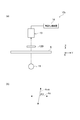
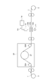
- FIG. 1 is a schematic diagram for explaining a defect inspection method for a light-transmitting film according to the first embodiment.
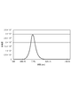
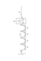
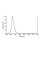
- FIG. 2 is a diagram illustrating an example of a spectral spectrum of illumination light used in the defect inspection method for the light transmissive film illustrated in FIG. 1.
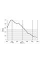
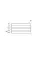
- FIG. 3 is a diagram illustrating an example of detection sensitivity characteristics of the imaging apparatus used in the defect inspection method for the light transmissive film illustrated in FIG. 1.
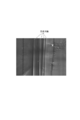
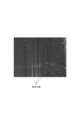
- FIG. 4 is a diagram showing a defect detection result when the difference between the maximum intensity wavelength of illumination light and the maximum sensitivity wavelength of the imaging device is 50 nm or less.
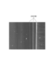
- FIG. 5 is a diagram showing a defect detection result when the difference between the maximum intensity wavelength of illumination light and the maximum sensitivity wavelength of the imaging device exceeds 50 nm.
- FIG. 1 is a schematic diagram for explaining a defect inspection method for a light-transmitting film according to the first embodiment.
- FIG. 2 is a diagram illustrating an example of a spectral spectrum of illumination light used
- FIG. 6 is a schematic diagram for explaining a defect inspection method for a light-transmitting film according to the second embodiment.
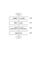
- FIG. 7 is a flowchart showing an example of a method for producing a linear polarizer film according to the third embodiment.
- FIG. 8 is a drawing for explaining a stretching process and a defect inspection process in the method of manufacturing the linear polarizer film shown in FIG.
- FIG. 9 is a drawing for explaining the process from the swelling process to the drying process in the method of manufacturing the linear polarizer film shown in FIG.
- FIG. 10 is a view for explaining a modification in the case where a defect inspection process is performed after the dyeing process in the method of manufacturing the linear polarizer film shown in FIG.
- FIG. 11 is a flow chart showing a modification in the case of further carrying out a protective film bonding step in the method of manufacturing the linear polarizer film shown in FIG.
- FIG. 12 is a drawing for explaining a protective film bonding step in the modification shown in the flowchart shown in FIG. 11.
- FIG. 13 is a schematic diagram illustrating the configuration of a polarizing plate manufactured by the polarizing plate manufacturing method according to the fourth embodiment.
- FIG. 14 is a flowchart illustrating an example of a polarizing plate manufacturing method according to the fourth embodiment.
- FIG. 15 is a schematic diagram for explaining another example of the defect inspection method for the light transmissive film.
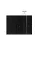
- FIG. 16 shows defect detection when the difference between the maximum intensity wavelength of light incident on the imaging device and the maximum sensitivity wavelength of the imaging device is 20 nm or less, using the defect inspection method for the light transmissive film shown in FIG. It is drawing which shows a result.
- FIG. 17 is a diagram showing a spectrum of blue light output from the blue LED used in the experiment.
- FIG. 18 is a diagram showing a spectral spectrum of red light output from the red LED used in the experiment.
- FIG. 19 is a diagram showing a defect detection result when the difference between the maximum intensity wavelength of illumination light and the maximum sensitivity wavelength of the imaging device is 50 nm or less.
- FIG. 20 is a diagram illustrating a defect detection result when the difference between the maximum intensity wavelength of illumination light and the maximum sensitivity wavelength of the imaging apparatus is 50 nm or less.
- the film S to be inspected is a raw material film used for manufacturing a linear polarizer film having linear polarization characteristics that transmits predetermined linearly polarized light.
- raw material films are polyvinyl alcohol (hereinafter sometimes referred to as “PVA”) resin films, polyvinyl acetate resin films, ethylene / vinyl acetate (hereinafter sometimes referred to as “EVA”) resin films, polyamide resin films. And a polyester resin film.
- PVA polyvinyl alcohol
- EVA ethylene / vinyl acetate
- EVA ethylene / vinyl acetate
- a polyester resin film Usually, from the viewpoint of the adsorptivity and orientation of the dichroic dye, a PVA-based resin film, particularly a PVA film having vinyl alcohol alone as a repeating unit is used.
- the thickness of the raw material film as the film S to be inspected is usually 1 ⁇ m or more and 50 ⁇ m or less.
- the linear polarizer film is manufactured through a polarization property imparting process that imparts a linear polarization property to the raw material film.
- the polarization property imparting treatment includes uniaxially stretching the raw material film and dyeing with a dichroic dye.
- Film material to be tested by the first inspection device 10 1 may also be before those polarization characteristic applying process is performed, or may be in the polarization characteristic applying process.
- Examples of detected defects include streak defects, dents, and minute foreign matter.
- a “streaky defect” is a defect that rises slightly in one direction (for example, about 1 ⁇ m).
- the “dent” is a recess having a diameter of 500 ⁇ m to 700 ⁇ m and a depth of about 0.2 ⁇ m to 0.5 ⁇ m.
- Examples of the recess are a small and deep recess having a diameter of about 500 ⁇ m and a depth of about 0.5 ⁇ m, a diameter of 700 ⁇ m and A relatively large and shallow recess having a depth of about 0.2 ⁇ m is included.
- Examples of “fine foreign matter” include foreign matter having a diameter of about 500 ⁇ m.
- the first inspection apparatus 10 1 comprises a pair of linear polarizer 12A, and 12B, a light source 11, an imaging device 13, and an image processing apparatus 14.
- a XYZ coordinate system is set as shown in FIG.
- the Z-axis direction is the thickness direction of the linearly polarizing plates 12A and 12B
- the Y-axis direction is the left-right direction in FIG.
- the pair of linearly polarizing plates 12A and 12B are arranged in parallel to each other.
- the linear polarizing plate 12A and the linear polarizing plate 12B have an absorption axis A 12A of the linear polarizing plate 12A and an absorption axis A 12B of the linear polarizing plate 12B. They are arranged so as to cross each other at a predetermined angle ⁇ 1 of 1.
- the absorption axis A 12A and the absorption axis A 12B intersect means that they intersect when viewed from the thickness direction (Z-axis direction) of the film S to be inspected.
- the first predetermined angle ⁇ 1 an angle at which a defect can be easily detected in an image obtained by imaging the film S to be inspected by the imaging device 13 is selected.
- the first predetermined angle ⁇ 1 is 85 ° to 90 °, preferably 89 ° to 90 °, more preferably 89.4 ° or more.
- the first predetermined angle ⁇ 1 is 90 ° to 95 °, preferably 90 ° to 91 °, more preferably 90.6 ° or less.
- the film S to be inspected is disposed in parallel with the linearly polarizing plates 12A and 12B between the pair of linearly polarizing plates 12A and 12B.
- the length in the X-axis direction of the linearly polarizing plates 12A and 12B can be the same as the length of the film S to be inspected in the X-axis direction, for example.
- the length in the Y-axis direction of the linearly polarizing plates 12A and 12B is usually equal to or shorter than the length in the Y-axis direction of the imaging region of the imaging device 13, and is usually shorter than the length in the Y-axis direction of the film S to be inspected.
- the light source 11 is disposed on the opposite side to the linearly polarizing plate 12B as viewed from the linearly polarizing plate 12A (below the linearly polarizing plate 12A in FIG. 1A) and emits illumination light for illuminating the film S to be inspected. Output.
- the illumination light output from the light source 11 is non-polarized light.
- An example of the light source 11 is a green LED that outputs green light as illumination light.
- An example of the wavelength range of the illumination light when the illumination light is green light is 440 nm to 590 nm.
- the illumination light is green light
- the illumination light has a light receiving area ⁇ (diameter).
- the light may be 1850 lux or more per mm.
- the imaging device 13 photographs the film S to be inspected through the linear polarizing plate 12B.
- the imaging device 13 is usually a monochrome camera.
- Examples of the imaging device 13 include a line sensor camera in which photodetectors are arranged in a line and an area sensor camera in which photodetectors are arranged in a two-dimensional manner.
- the imaging device 13 inputs the imaging result to the image processing device 14.
- the image processing device 14 includes a computer, and processes a signal indicating a result of photographing by the imaging device 13 to form a photographed image. At this time, in the film S to be inspected, a photographed image is formed so as to distinguish a defective portion where a defect has occurred from other normal portions. In order to distinguish the defective portion and the normal portion on the image, for example, a gray level difference may be given between them.
- the image processing apparatus 14 may include an image processing function that extracts a defective portion based on the formed captured image. Extraction of the defective portion includes, for example, coloring the defective portion.
- the image processing apparatus 14 may have a display that displays the formed image. Alternatively, separately from the image processing apparatus 14, the image processing apparatus 14 images the first inspection device 10 1 a display for displaying the formed can may have.
- the captured image of the imaging device 13 is a black and white (monochrome) image.
- the maximum intensity wavelength lambda] m s is the wavelength corresponding to the maximum intensity of the illumination light output from the light source 11, the wavelength corresponding to the maximum sensitivity of the imaging device 13 the difference between the maximum sensitivity wavelength lambda] m d is is a light source 11 and the imaging device 13 satisfy the relationship that is 50nm or less.
- Maximum intensity wavelength lambda] m s is also a wavelength corresponding to the maximum value of the light intensity in the spectrum of the illumination light.
- Maximum sensitivity wavelength lambda] m d of the image pickup device 13, specifically, the maximum sensitivity wavelength lambda] m d photodetector imaging apparatus 13 has.
- the difference between the maximum intensity wavelength lambda] m s and the maximum sensitivity wavelength lambda] m d is preferably 20nm or less.
- An example of illumination light output from the light source 11 is green light having a maximum intensity wavelength ⁇ m s having a maximum and maximum light intensity in a wavelength range of 515.5 nm to 516.5 nm, and the full width at half maximum of the spectrum of the green light. Is usually 50 nm or less, preferably 40 nm or less, and usually 10 nm or more.
- Examples of the illumination light in the visible light range normally 75nm or more from the maximum intensity wavelength lambda] m s, preferably usually 75nm or more wavelength ranges and lambda] m s below than 60 nm, preferably the light intensity in the wavelength range above or 60 nm, the maximum intensity The light is usually 25% or less, preferably 10% or less.
- Maximum sensitivity wavelength lambda] m d of the image pickup device 13, more specifically, examples of the maximum sensitivity wavelength lambda] m d photodetector imaging apparatus 13 has is 500 nm.
- the film S to be inspected is disposed between the pair of linearly polarizing plates 12A and 12B.
- the film to be inspected S is photographed by the imaging device 13 via the linearly polarizing plate 12B while outputting the illumination light from the light source 11.
- Illumination light from the light source 11 passes through the linear polarizing plate 12A and is applied to the film S to be inspected as linearly polarized light. Therefore, the linearly polarized light that has passed through the linearly polarizing plate 12A is irradiated as illumination light on the film S to be inspected. And the light which permeate
- the linearly polarizing plate 12B is arranged with respect to the linearly polarizing plate 12A in a state where the absorption axes A 12A and A 12B intersect at a first predetermined angle ⁇ 1.
- linear polarizer 12B the absorption axis A 12B is disposed so as to intersect at a first predetermined angle ⁇ 1 with respect to the plane of vibration of linearly polarized light is an illumination light irradiating the object to be inspected film S . Therefore, in a normal part where no defect is generated in the film S to be inspected, the light transmitted through the film S to be inspected is hardly transmitted through the linearly polarizing plate 12B. On the other hand, if the film S to be inspected has a defect, the polarization of the linearly polarized light transmitted through the defective part is disturbed. Thereby, the light that has passed through the defective portion is likely to pass through the linearly polarizing plate 12B. Therefore, more light that has passed through the defective portion is incident on the imaging device 13 than light that has passed through the normal portion.
- the image processing apparatus 14 can confirm the defective portion by forming a captured image in which the normal portion and the defective portion are represented by shading according to the luminance.
- the difference between the maximum intensity wavelength lambda] m s with the illumination light irradiated to the inspected film S, a maximum sensitivity wavelength lambda] m d of the image pickup device 13 is 50nm or less.
- the defect inspection method using the first inspection apparatus 10 can detect defects with high sensitivity is there.
- the maximum intensity wavelength lambda] m s of the illumination light the difference between the maximum sensitivity wavelength lambda] m d of the image pickup device 13 is greater than 50 nm, of the defect, for example, a defect slightly raised extends in one direction muscle The defect cannot be detected.
- the maximum intensity wavelength lambda] m s of the illumination light, the difference between the maximum sensitivity wavelength lambda] m d of the image pickup device 13 is equal to 50nm or less, it is possible to detect a line defect.
- the imaging device 13 when green light is taken as illumination light, it is easy to obtain a high contrast image (particularly a grayscale image). And when green light is used for illumination light, the imaging device 13 also has high sensitivity to green light. Therefore, since the light output from the light source 11 is green light, the defective portion and the normal portion can be more clearly distinguished. As a result, the defective portion, in particular, the streak defect that could not be detected in the related art is obtained. It can be detected more reliably.
- the linearly polarizing plates 12A and 12B tend to absorb green light. Therefore, in the form in which green light is output from the light source 11, if the illuminance of the illumination light output from the light source 11 is high, for example, if the illuminance is 1850 lux or more per light receiving area ⁇ 1 mm, it is easy to detect a defect.
- the first predetermined angle ⁇ 1 is 85 ° to 90 °, preferably 89 ° to 90 °, more preferably 89.4 ° or more, or 90 ° to 95 °, preferably 90 ° to 91 °, and further In the form of preferably 90.6 ° or less, the absorption axis A 12A and the absorption axis A 12B substantially intersect at 90 °. For this reason, the light that has passed through the defective portion is incident on the imaging device 13, while the light that has passed through the normal portion is not substantially incident. Therefore, it is easier to distinguish a normal part and a defective part.
- the first inspection device 10 1 Using the experimental results, the first inspection device 10 1 will be described that can be more reliably detect defects.
- Experiments E1 and E2 were performed as experiments. In the description of the experiment E1, E2, for convenience of description, components corresponding to the first inspection apparatus 10 1 constituent components are denoted by the same reference numerals.
- E2 also was adopted a first inspection device 10 1 having the structure shown in Figure 1 (a).
- a green LED that outputs green light was used as the light source 11.
- the spectrum of the illumination light output from the green LED used in Experiment E1 is as shown in FIG.
- the horizontal axis in FIG. 2 indicates the wavelength (nm), and the vertical axis indicates the relative light intensity (arbitrary unit).
- the maximum intensity wavelength lambda] m s of the illumination light in the experiment E1 is 516 nm
- the full width at half maximum of the spectrum is green light is 39.5 nm.
- a white LED that outputs white light was used as the light source 11.
- Maximum intensity wavelength lambda] m s of the illumination light outputted from the light source 11 of the experiment E2 is 425 nm.
- the same imaging device 13 was used in the experiments E1 and E2.
- the detection sensitivity characteristics of the imaging device 13 are as shown in FIG. In FIG. 3, the horizontal axis indicates the wavelength (nm), and the vertical axis indicates the relative value normalized by the maximum sensitivity. As shown in FIG. 3, the maximum sensitivity wavelength lambda] m d of the imaging device 13 is 500 nm.
- the difference between the maximum sensitivity wavelength lambda] m d of the image pickup device 13 at 16nm is there. That is, in the experiment E1, the difference between the maximum intensity wavelength lambda] m s and the maximum sensitivity wavelength lambda] m d, and a 50nm or less, more particularly, to 20nm or less. Meanwhile, in Experiment E2, the difference between the maximum intensity wavelength lambda] m s of the illumination light, the maximum sensitivity wavelength lambda] m d of the image pickup device 13 is 75 nm. That is, in experimental E2, the difference between the maximum intensity wavelength lambda] m s and the maximum sensitivity wavelength lambda] m d is over 50nm.
- the film S to be inspected is a uniaxially stretched polyvinyl alcohol (PVA) film. Since the PVA film absorbs moisture and wrinkles easily occur, PVA films manufactured under the same conditions were prepared in Experiments E1 and E2. The thickness of the PVA film as the film S to be inspected was 8 ⁇ m in both Experiment E1 and Experiment E2.
- PVA polyvinyl alcohol
- each of the inspected films S was placed between the linearly polarizing plates 12A and 12B, and then the illumination light was output from the light source 11. And the defect was test
- the linearly polarizing plates 12A and 12B were arranged so that the first predetermined angle ⁇ 1 was 90 °.
- the maximum intensity wavelength lambda] m s of the illumination light is set to lower than or equal to 50nm the difference between the maximum sensitivity wavelength lambda] m d of the image pickup device 13 is capable of detecting defects more reliably, in particular, a line defect It is understood that it can be detected properly.
- the linear polarization characteristic i.e., a light transmissive film having an absorption axis A S.
- the linear polarizer film which transmits linearly polarized light polarized in the direction orthogonal to the direction of the absorption axis A S, and a protective film on at least one side of the linear polarizer film is laminated Laminated polarizer film.
- the protective film is a transparent light-transmitting film, and examples of the protective film include triacetyl cellulose (hereinafter sometimes referred to as “TAC”) film, polyethylene terephthalate film, nylon film, polycarbonate film, polyethylene film, and the like. Including. Usually, a TAC film having a small optical anisotropy, particularly a TAC film made of a homopolymer of triacetyl cellulose is used.
- TAC triacetyl cellulose
- the thickness of the laminated polarizer film as the inspected film S is usually 5 ⁇ m to 300 ⁇ m (0.3 mm).
- the second inspection device 10 2 in that it does not comprise a linear polarizer 12A, mainly different first inspection apparatus 10 1. Focusing on this difference the second inspection device 10 2 will be described.
- the inspected film S and the linear polarization plate 12B as shown schematically in FIG. 6 (b), the absorption the absorption axis A 12B linear polarizer 12B is inspected film S placement against the axis a S while intersecting at a second predetermined angle .theta.2.
- the second predetermined angle ⁇ 2 an angle at which a defect can be easily detected in an image obtained by imaging the film S to be inspected by the imaging device 13 can be selected.
- the second predetermined angle ⁇ 2 may be the same as the first predetermined angle ⁇ 1.
- the second predetermined angle ⁇ 2 may be 85 ° to 90 °, preferably 89 ° to 90 °, more preferably 89.4 ° or more.
- the second predetermined angle ⁇ 2 may be 90 ° to 95 °, preferably 90 ° to 91 °, more preferably 90.6 ° or less.
- the light to be inspected is irradiated with illumination light from the light source 11. Since the film S to be inspected has linear polarization characteristics, the light that has passed through the normal part in the film S to be inspected where no defect has occurred is linearly polarized light.
- the linearly polarizing plate 12B is arranged so as to intersect the film S to be inspected at the second predetermined angle ⁇ 2, most of the linearly polarized light transmitted through the normal part of the film S to be inspected The light is absorbed by the linearly polarizing plate 12B and does not pass through it. That is, the linearly polarized light transmitted through the normal part is difficult to transmit through the linearly polarizing plate 12B.
- the linear polarization characteristic of the inspected film S is disturbed in the defective part.
- the light transmitted through the defective portion includes light having a polarization component different from the linearly polarized light generated in the inspected film S.
- the light transmitted through the defective portion of the film S to be inspected easily passes through the linearly polarizing plate 12B.
- more light that has passed through the defective portion than light that has passed through the normal portion passes through the linearly polarizing plate 12B and is incident on the imaging device 13 as incident light.
- the imaging apparatus the difference between the maximum sensitivity wavelength lambda] m d 13 is 50nm or less. Therefore, when the film to be inspected S has a defect, the brightness difference is more clearly generated between the normal part and the defective part. As a result, defects can be detected in the same manner as in the first embodiment.
- the second inspection device 10 2 In the second inspection device 10 2, the inspection film S and the linear polarization plate 12B, the absorption axis A S, A 12B are arranged in a state that intersect at a second predetermined angle .theta.2, to be inspected film S and the maximum intensity wavelength lambda] m s of illumination light irradiated has, since the difference between the maximum sensitivity wavelength lambda] m d of the image pickup device 13 is 50nm or less, the second inspection device 10 2, in the case of the first inspection apparatus 10 1 In the same manner, the defect of the film S to be inspected can be inspected. Therefore, a defect inspection method using the second inspection device 10 2 has at least same effect as a defect inspection method in the case of using the first inspection apparatus 10 1 in the first embodiment.
- the linear polarizer film is produced by subjecting an unstretched and undyed raw film to a polarization property imparting treatment that imparts a linear polarization property.
- the example of the raw material film for manufacturing a linear polarizer film is the same as the film illustrated in 1st Embodiment.
- a PVA film particularly a PVA film is usually used.
- a raw material film is strip
- the manufacturing method of the linear polarizer film includes a stretching step S10 for uniaxially stretching a raw material film, a defect inspection step S11 for inspecting a defect of the uniaxially stretched raw material film, and a uniaxially stretched raw material. And a dyeing process S13 for dyeing the film with a dichroic dye.
- a stretching step S10 for uniaxially stretching a raw material film a defect inspection step S11 for inspecting a defect of the uniaxially stretched raw material film, and a uniaxially stretched raw material.
- a dyeing process S13 for dyeing the film with a dichroic dye.
- FIG. 7 it has a swelling treatment step S12 before the dyeing treatment step S13, and after the dyeing treatment step S13, a boric acid treatment step S14, a water washing treatment step S15 and a drying step S16. You may have.
- Each step illustrated in FIG. 7 will be described with reference to FIGS. 8 and 9. Below, the form containing swelling process process S12, boric-acid process process S14, water washing process process S17, and drying process S16 is illustrated and demonstrated.
- the raw material film 1 is fed out from the first raw material film roll 2 in which the belt-shaped raw material film 1 is wound in a roll shape, and the raw material is drawn by the conveying roller.
- the film 1 is conveyed to the stretching device 20.
- the uniaxially stretched raw material film 1 is unloaded from the stretching device 20.
- the stretching device 20 includes a heat roll 21 and transport rollers 22A and 22B disposed before and after the heat roll 21 in the transport direction of the raw material film 1.
- the positions of the transport rollers 22 ⁇ / b> A and 22 ⁇ / b> B and the position of the heat roll 21 are different.
- the raw material film 1 is passed over the heat roll 21, and is tensioned in the conveyance direction (longitudinal direction) of the raw material film 1 by the conveyance rollers 22 ⁇ / b> A and 22 ⁇ / b> B before and after the heat roll 21 in the conveyance direction of the raw material film 1.
- the raw material film 1 is uniaxially stretched. Examples of the draw ratio are 3 to 8 times.
- the raw film 1 is uniaxially stretched using the heat roll 21.
- the raw film 1. May be uniaxially stretched.
- (3-2) Defect Inspection Step In the defect inspection step S11, as shown in FIG. 8, the raw film 1 carried out from the stretching apparatus 20 is used as the inspection film S, and the raw film 1 is inspected for defects. As shown in FIG. 7, when performing defect inspection between the stretching step S ⁇ b> 10 and the dyeing treatment step S ⁇ b> 13, the raw film 1 is not imparted with linear polarization characteristics. Therefore, the stretching step S10, with the dyeing step S13, when performing defect inspection by the defect inspection method using the first inspection apparatus 10 1 described in the first embodiment, inspection of defects.
- the first inspecting apparatus 10 in the downstream of the stretching device 20 is arranged on the transport path of the film material 1. Specifically, the raw material film 1 is passed between the linearly polarizing plates 12A and 12B arranged in a state where the absorption axes A 12A and A 12B intersect at the first predetermined angle ⁇ 1. At that time, illumination light is output from the light source 11, and the raw material film 1 is photographed by the imaging device 13 via the linear polarizing plate 12 ⁇ / b> B. A captured image is formed in the image processing device 14 on the basis of the photographing result of the imaging device 13. The presence or absence of a defect can be determined by looking at this captured image.
- the two linearly polarizing plates 12A and 12B are arranged so as to intersect at the first predetermined angle ⁇ 1, the normal part having no defect is transmitted through the inspected film S.
- the incident light is difficult to enter the imaging device 13.
- the linearly polarized light transmitted through the linearly polarizing plate 12A is disturbed in the defective portion, so that the light transmitted through the raw material film 1 as the film S to be inspected is linearly polarized light. It is easy to enter the imaging device 13 through the plate 12B. That is, when the raw material film 1 has a defective portion, the light transmitted through the defective portion is incident on the imaging device 13 more than the light transmitted through the normal portion.
- the difference between the maximum intensity wavelength lambda] m s with the illumination light irradiated to the inspected film S, a maximum sensitivity wavelength lambda] m d of the image pickup device 13 is 50nm or less.
- the defect position may be recorded electronically on a recording medium, for example, or may be recorded by marking a defective portion of the raw material film 1 with a marker or the like.
- the recording medium may be, for example, a storage unit in the image processing apparatus 14, a storage unit of another computer, or a removable external recording medium such as a USB memory and a DVD.
- Film material 1 which has passed through the first inspection apparatus 10 1 is wound into a roll.
- the roll on which the stretched raw film 1 is wound is referred to as a second raw film roll 3.
- the uniaxially stretched raw material film 1 fed out from the second raw material film roll 3 is immersed in a treatment bath in the swelling tank 30.
- the raw material film 1 is subjected to a swelling treatment.
- This swelling treatment is performed for the purpose of removing foreign matter on the film surface, removing the plasticizer in the film, imparting easy dyeability in a subsequent process, and plasticizing the raw film 1.
- the conditions for the swelling treatment can be determined within a range in which these objects can be achieved, and in a range in which problems such as extreme dissolution and devitrification of the raw material film 1 do not occur.
- the swelling treatment is performed by immersing the raw material film 1 in a treatment bath at a temperature of 10 to 50 ° C., preferably 20 to 50 ° C., for example.
- the swelling treatment time is about 5 to 300 seconds, preferably about 20 to 240 seconds.
- the treatment bath used in the swelling tank 30 is pure water, boric acid as described in JP-A-10-153709, chloride as described in JP-A-6-281816, and others.
- An aqueous solution to which an inorganic acid, other inorganic salt, a water-soluble organic solvent, alcohols and the like are added in an amount of 0.01 to 10% by weight can be used.
- pure water substantially free from dissolved components is preferably used.
- the raw material film 1 that has undergone the swelling process step S12 is immersed in an aqueous solution of the dichroic dye in the dyeing tank 31, thereby making the raw material film 1 with the dichroic dye. Stain.
- a normal dyeing process with a dichroic dye is performed for the purpose of adsorbing the dichroic dye on the raw film 1.
- the processing conditions are determined within a range in which such an object can be achieved and in a range in which problems such as extreme dissolution and devitrification of the raw material film 1 do not occur.
- Examples of dichroic dyes used for dyeing are iodine and dichroic dyes.
- iodine is 0.003 to 0.2 parts by weight and iodine at a temperature of 10 to 50 ° C., preferably 20 to 40 ° C., and 100 parts by weight of water.
- the dyeing treatment is performed by immersing the raw material film in an aqueous solution containing 0.1 to 10 parts by weight of potassium halide for 10 to 600 seconds, preferably 30 to 200 seconds.
- potassium iodide other iodides such as zinc iodide may be used.
- Other iodides may be used in combination with potassium iodide.
- iodide compounds other than iodide, such as boric acid, zinc chloride, cobalt chloride, etc. may coexist. Even when boric acid is added, it is distinguished from the subsequent boric acid treatment in that it contains iodine. Any bath containing 0.003 parts by weight or more of iodine with respect to 100 parts by weight of water can be regarded as a dyeing bath.
- the dichroic dye When a water-soluble dichroic dye is used as the dichroic dye, the dichroic dye is added at a temperature of, for example, 20 to 80 ° C., preferably 30 to 60 ° C., and 100 parts by weight of water.
- the dyeing process is performed by immersing the raw material film 1 in an aqueous solution containing 0.1 part by weight for 10 to 600 seconds, preferably 20 to 300 seconds.
- the aqueous solution of the dichroic dye to be used may contain a dyeing assistant or the like, and may contain, for example, an inorganic salt such as sodium sulfate or a surfactant. Only one type of dichroic dye may be used, or two or more types of dichroic dyes may be used in combination according to the desired hue.
- the dichroic dye is adsorbed and oriented on the raw film 1 in the stretching direction of the uniaxial stretching through the dyeing process S13.
- the linear polarization property is imparted to the raw material film 1. Therefore, in the manufacturing method according to the flowchart shown in FIG. 7, the raw material film 1 after the dyeing process step S ⁇ b> 13 is the linear polarizer film 4.
- the film processed at each process after dyeing process S13 is also explained as raw material film 1.
- the raw film 1 that has undergone the dyeing treatment step S13 is immersed in an aqueous solution in the boric acid bath 32 to perform boric acid treatment.
- This boric acid treatment is performed by immersing the raw material film 1 dyed with a dichroic dye in an aqueous solution containing about 1 to 10 parts by weight of boric acid with respect to 100 parts by weight of water.
- the boric acid treatment bath preferably contains about 0.1 to 30 parts by weight of iodide with respect to 100 parts by weight of water in addition to boric acid.
- iodide include potassium iodide and zinc iodide.
- This boric acid treatment is performed for water resistance and hue adjustment (to prevent bluish tint) by crosslinking.
- a cross-linking agent such as glyoxal or glutaraldehyde can be used together with boric acid as necessary.
- the boric acid treatment for water resistance is sometimes referred to as water resistance treatment, crosslinking treatment, immobilization treatment, or the like.
- boric acid treatment is regarded as hue adjustment, and is sometimes referred to as complementary color processing, toning processing, or the like.
- This boric acid treatment is performed by appropriately changing the concentration of boric acid and iodide and the temperature of the treatment bath according to the purpose.
- the boric acid treatment for water resistance and the boric acid treatment for hue adjustment are not particularly distinguished, but are preferably carried out under the following conditions.
- boric acid is about 3 to 10 weights per 100 weight parts of water.
- An aqueous solution containing about 1 to 20 parts by weight of iodide and iodide is used as a boric acid treatment bath, usually at a temperature of 50 to 70 ° C., preferably 53 to 65 ° C.
- the treatment time is usually about 10 to 600 seconds, preferably 20 to 300 seconds, more preferably 20 to 100 seconds.
- boric acid treatment for hue adjustment may be further performed.
- the dichroic dye is iodine
- an aqueous solution containing about 1 to 5 parts by weight of boric acid and about 3 to 30 parts by weight of iodide for 100 parts by weight of water is used for this purpose.
- An acid treatment bath is usually used at a temperature of about 10 to 45 ° C.
- the immersion time is usually about 1 to 300 seconds, preferably 2 to 100 seconds.
- the boric acid treatment for hue adjustment is usually performed at a lower temperature than the boric acid treatment for water resistance.
- this boric acid treatment may be performed in a plurality of tanks, and usually 1 to 5 tanks are often arranged.
- the raw material film 1 sequentially passes through each tank, and the raw film 1 is subjected to boric acid treatment.
- positioning a some tank the aqueous solution composition and temperature of each boric-acid processing tank to be used may be the same within the said range, or may differ.
- the boric acid treatment for water resistance and the boric acid treatment for hue adjustment may be performed in a plurality of tanks, respectively.
- water-washing process S15 the raw material film 1 which passed through the boric-acid treatment process S14 is immersed in the water in the water-washing tank 33, and the raw material film 1 after the boric-acid treatment process S14 is washed with water.
- the water washing treatment may be performed by a method of spraying water as a shower or a method of using immersion and spraying together.
- the water temperature in the water washing treatment is usually about 2 to 40 ° C., and the treatment time is usually about 2 to 120 seconds.
- the drying step S16 the raw material film 1 that has undergone the water washing treatment step S15 is conveyed to the drying device 34, and the raw material film 1 is dried in the drying device 34.
- This drying is performed for about 30 to 600 seconds in the drying apparatus 34 maintained at a temperature of about 40 to 100 ° C.
- FIG. 9 schematically shows the drying device 34.
- the drying device 34 is not particularly limited as long as the moisture attached to the raw material film 1 can be dried by the drying step S16, and may be a known device that is usually used in the production of a linear polarizer film.
- the defect inspection step S11 is performed after the stretching step S10. Therefore, it is possible after fed from the first raw material film roll 2, to inspect the defects generated in the raw material film 1 to reach the first inspection device 10 1.
- defect inspection is performed by the inspection method described in the first embodiment. Therefore, when the raw material film 1 has a defect, the defective portion can be detected more reliably.
- defects for example, point-like defects
- a streak defect may occur.
- Such a streak defect could not be detected by a conventional inspection method.
- using the illumination light and the image pickup device 13 to satisfy the relationship that the difference between the maximum intensity wavelength lambda] m s and the maximum sensitivity wavelength lambda] m d is 50nm or less By performing the defect inspection, the streak defect can also be detected in the defect inspection step S11. In the form in which the illumination light is green light, it is easier to detect the streak defect.
- the defect inspection process S11 is provided after extending process S10 as shown in FIG. 7, the said streak defect can be detected reliably.
- a defect When a defect is detected by defect inspection, it is possible to record the defect position electronically or mark the defect portion of the raw film 1 as described above.
- a polarizing plate is manufactured using the linear polarizer film 4 by performing the recording process (recording process) as described above while performing the defect inspection process S11 or after the defect inspection process S11, the defect portion It is possible to manufacture a polarizing plate while avoiding the above, or to easily sort a polarizing plate including a defective portion from the manufactured polarizing plate. As a result, it is easy to obtain a polarizing plate as a good product.
- the defect state for example, the number or size of a defective part
- production of linear polarizer film 4 is interrupted and the first raw material film roll 2 is made. It may be replaced.
- the post-process can be omitted for the raw material film 1 whose defect state exceeds the allowable range, the linear polarizer film 4 as a non-defective product can be efficiently manufactured.
- the determination as to whether or not to stop the production of the linear polarizer film 4 may be made, for example, while viewing the photographed image formed by the image processing device 14 in the defect inspection step S11, or the second raw film roll After forming 3, the defect state over the entire length of the raw material film 1 wound around the second raw material film roll 3 may be taken into consideration.
- the defect inspection step S11 may not be provided between the stretching step S10 and the swelling treatment step S12, and may be performed while the polarization property imparting step for imparting linear polarization properties to the raw film 1 is being performed.
- the defect inspection process S11 may be performed between the swelling process step S12 and the dyeing process step S13.
- the first inspection apparatus 10 1 is provided in the transport path of the film material 1 from swelling bath 30 to dyeing tank 31.
- the defect inspection step S11 is provided between the swelling treatment step S12 and the dyeing treatment step S13, it is possible to inspect the defects generated up to the swelling treatment step S12, and a linear polarizer according to the inspection result. Whether or not the film 4 can be manufactured can be determined.
- the defect inspection step S11 may be provided before the stretching step S10, that is, before the polarization property imparting step for imparting linear polarization properties to the raw material film 1.
- the raw material film 1 itself wound around the first raw material film roll 2 is inspected. Thereby, it is possible to inspect the defect when the raw material film 1 is manufactured with high sensitivity.
- defect inspection process S11 of the modification 2 when the raw material film 1 has a defect exceeding an allowable range, for example, if the first raw material film roll 2 is replaced, the process after the stretching process S10 exceeds the allowable range.
- a more appropriate raw material film 1 can be used. As a result, the production efficiency of the linear polarizer film 4 is improved.
- the defect inspection step S11 may be provided after the dyeing treatment step S13, that is, after the polarization property imparting step for imparting the linear polarization property to the raw material film 1.
- the linear polarizer film 4 since it passes through extending process S10 and dyeing process S13, the linear polarizer film 4 by which the linearly polarized light characteristic was provided to the raw material film 1 will be test
- the raw material film 1 is uniaxially stretched in the conveying direction of the raw material film 1, that is, in the longitudinal direction of the raw material film 1. Since the direction of the absorption axis A S corresponds to the stretching direction, the direction of the absorption axis A S given to the film material 1 by the raw material film 1 is subjected to the stretching step S10 and dyeing process S13., Substantially It can be assumed that the material film 1 (or the linear polarizer film 4) is conveyed.
- the absorption axis A 12B linear polarizer 12B intersect at a second predetermined angle ⁇ 2 with respect to the transport direction them if, linear polarizer 12B is with respect to the linear polarizer film 4 being conveyed, at a second predetermined angle ⁇ 2 absorption axis a 12B linear polarizer 12B is with respect to the absorption axis a S of the linear polarizer film 4 It will be arranged in a crossing state.
- the conveying direction of the film material 1 exemplifies a case it is assumed that the direction of the absorption axis A S, for example, prior to the defect inspection step S11 in the modified example 3, detects the direction of the absorption axis A S, the The arrangement of the linearly polarizing plate 12B may be adjusted using the detection result.
- the second inspection device 10 2 uses the second inspection device 10 2, the method of defect inspection of the inspected film S which is a linear polarizer film 4, because it is as described in the second embodiment, the description thereof is omitted.
- the difference between the maximum intensity wavelength lambda] m s and the maximum sensitivity wavelength lambda] m d is using illumination light and the imaging device 13 is 50nm or less, the detection sensitivity of the defect Is good. Therefore, it is possible to detect the defect more reliably, and in particular, it is possible to detect a streak defect that may occur in the stretching step S10. In the form in which the illumination light is green light, it is easier to detect the streak defect.
- Modification 3 it is possible to detect with high sensitivity defects generated in the process until the linear polarizer film 4 is manufactured. As a result, whether or not the raw material film 1 to which the linearly polarized light property is imparted is appropriate as the linear polarizer film 4 as a product, or the linear polarizer film 4 is produced following the production of the linear polarizer film 4. It can be judged more appropriately whether it can be used for manufacture of a polarizing plate.
- the second inspection device 10 2 is arranged downstream of the drying device 34, and by using the second inspection device 10 2 carried a defect inspection step S11.
- the raw film 1 is given a linear polarization characteristic, and therefore the defect inspection step S11 described in the modified example 3 may be performed after the dyeing treatment step S13.
- the defect inspection step S11 and the second inspection device 10 2 is provided in the transport path of the film material 1 from dyeing tank 31 to the washing tank 33.
- the protective film 5 is a transparent film for protecting the linear polarizer film 4.
- the example of the protective film 5 is the same as the film illustrated about the protective film in 2nd Embodiment.
- a TAC film particularly a TAC film is used.
- An example of the thickness of the protective film 5 is 10 ⁇ m to 100 ⁇ m.
- the adhesive surface with the linear polarizer film 4 may be subjected to a hydrophilic treatment such as a saponification treatment.
- the linear polarizer film 4 is fed by a roll-to-roll method by feeding the protective film 5 out of a protective film roll 6 in which the protective film 5 is wound in a roll shape.
- a protective film 5 is laminated on the substrate.
- the protective film 5 is laminated on both sides of the linear polarizer film 4, but the protective film 5 may be laminated only on one side.
- a water-soluble adhesive for bonding them is usually applied to the interface. Therefore, usually, after the protective film 5 is laminated on the linear polarizer film 4, the protective film 5 is carried into the drying device 40 to dry the adhesive, and the protective film 5 and the linear polarizer film 4 are bonded together.
- FIG. 12 schematically shows the drying device 40.
- the drying device 40 is not particularly limited as long as the laminated polarizer film 7 can be dried, and may be a known device used for manufacturing a linear polarizer film.
- Modification 5 As described in the modified example 4, when a protective film laminating step S17, as illustrated in FIG. 12, downstream of the drying device 40, and the second inspection unit 10 2 is disposed, the defect inspection step S11 may be performed. Method of inspecting a laminated polarizer film 7 by the second inspection device 10 2 may be the same as in the case described in the second embodiment and the third modification.
- the laminated polarizer film 7 is inspected by the defect inspection method described in the second embodiment using the film to be inspected S, it occurs in the process until the laminated polarizer film 7 is manufactured including the defects of the protective film 5 itself.
- the detected defect can be detected with high sensitivity.
- whether the laminated polarizer film 7 as the linear polarizer film 4 on which the protective film 5 is laminated is appropriate as a linear polarizer film as a product, or manufacture of a polarizing plate using the laminated polarizer film 7 It is possible to more appropriately determine whether or not it can be used.
- defect inspection process S11 When performing defect inspection process S11 after protective film bonding process S17, defect inspection process S11 may be implemented separately by protective film bonding process S17, or does not need to be implemented.
- the dyeing process S13 is performed after the stretching process S10.
- the stretching step S10 may be performed after the dyeing step S13.
- the dyeing process S13 is performed before the stretching process S10, the swelling process S12, the boric acid process S14, the water washing process S15 and the drying process S16 are also performed before the stretching process S10.
- the defect inspection step S11 may be performed after the stretching step S10.
- the stretching process S10 is performed after the dyeing process S13, in FIG. 8, instead of the raw material film 1 fed out from the first raw film roll 24, the raw material film 1 that has been dyed and dried is stretched by the stretching device 20. Just bring it in. Then, the first place of the inspection apparatus 10 1 shown in FIG. 8, may be used a second inspection device 10 2.
- the stretching process S10 may be performed during the dyeing process S13.
- the raw film 1 in the conveyance direction of the raw material film 1, the raw film 1 is immersed in the aqueous solution of the dichroic dye in the dyeing tank 31 by setting the peripheral speeds of the conveying rollers before and after the dyeing tank 31 to different peripheral speeds.
- the raw material film 1 can be uniaxially stretched in the longitudinal direction (conveyance direction) while performing the dyeing treatment.
- the stretching step S10 may be performed during the boric acid treatment step S14, or may be performed over the dyeing treatment step S13 and the boric acid treatment step S14.
- the polarizing plate 50 includes a laminated polarizer film 7 composed of a linear polarizer film 4 and protective films 5 bonded to both surfaces thereof, and a protect provided on one protective film 5. It has a film 51, an adhesive layer 52 provided on the other protective film 5, and a separate film 53 provided on the adhesive layer 52.
- the planar view shape (the shape seen from the thickness direction) of the polarizing plate 50 may be any one according to the device to which the polarizing plate 50 is applied.
- the example of the planar view shape of the polarizing plate 50 is a rectangle or a square.
- the linear polarizer film 4 is manufactured through a process before the protective film 5 is bonded as described in the third embodiment. Since the protective film 5 is the same as the protective film described in Modification 4 of the third embodiment, the description thereof is omitted.
- the protect film 51 is a surface protective film for protecting the surface of the laminated polarizer film 7.
- An example of the thickness of the protect film 51 is 30 ⁇ m to 100 ⁇ m.
- Examples of the material of the protective film 51 include polyethylene, polypropylene, and polyester.
- the adhesive layer 52 is for attaching the polarizing plate 50 as a product to another member such as a liquid crystal cell.
- An example of the thickness of the adhesive layer 52 is 5 ⁇ m to 30 ⁇ m.
- the example of the adhesive which comprises the adhesion layer 52 contains an acrylic adhesive, a urethane adhesive, and a silicone adhesive.
- the separate film 53 is a film for preventing dust and the like from adhering to the adhesive layer 52 until the polarizing plate 50 as a product is used.
- An example of the thickness of the separate film 53 is 30 ⁇ m to 100 ⁇ m.
- the surface of the separation film 53 on which the adhesive layer 52 is formed is bonded to the protective film 5. Therefore, a member in which the adhesive layer 52 is formed on one surface of the separate film 53 is also referred to as a separate film 54 with an adhesive layer.
- the manufacturing method of the polarizing plate 50 includes a linear polarizer film manufacturing process S ⁇ b> 20 that manufactures the linear polarizer film 4, and a first method in which the protective film 5 is bonded to both surfaces of the linear polarizer film 4.
- the protective film 51 is bonded to one surface of the laminated polarizer film 7 that has undergone the bonding step (protective film bonding step) S21 and the first bonding step S21, and a separate film 54 with an adhesive layer is bonded to the other surface.
- the 2nd bonding process S22 which bonds, and the cutting process S23 which cuts out the polarizing plate 50 as a product from the laminated polarizer film 7 which passed 2nd bonding process S22.
- Each step will be described.
- the protective film 51 is laminated on one surface of the laminated polarizer film 7 by the same method as when the protective film 5 described with reference to FIG. A separate film 54 with an adhesive layer is laminated on the other surface.
- the protective film 51 is laminated on the laminated polarizer film 7 and the roll-to-roll method. Laminate by. At this time, an adhesive may be applied to the surface of the protect film 51 facing the laminated polarizer film 7.
- a separate film 54 with an adhesive layer is laminated on the laminated polarizer film 7 by a roll-to-roll method.
- the adhesive layer-attached separate film 54 may be laminated on the laminated polarizer film 7 so that the adhesive layer 52 is in contact with the laminated polarizer film 7 in the separate film 54 with the adhesive layer.
- the laminated polarizer film 7 that has undergone the second bonding step S22 is cut into the size of the polarizing plate 50 as a product to obtain the polarizing plate 50.
- the polarizing plate 50 may be cut out from the laminated polarizer film 7 so as not to include a defective portion according to the inspection result of the defect inspection step S11 (see FIG. 7) in the manufacturing process of the linear polarizer film 4. .
- the linear polarizer film 4 included in the laminated polarizer film 7 is manufactured by the manufacturing method illustrated in FIG. Therefore, the linear polarizer film 4 is manufactured through defect inspection process S11 (refer FIG. 7).
- the cutting step S23 based on the defect detection result in the defect inspection step S11, it is possible to select the portion where no defect has occurred and cut out the polarizing plate 50. As a result, it is easy to manufacture a polarizing plate 50 that does not include defects.
- a defect is detected in the defect inspection step S11, if the defect position is recorded, it is easy to select the portion where no defect has occurred and cut out the polarizing plate 50.
- the polarizing plate 50 that does not include a defective portion may be sorted. For example, if the inspection result of the defect inspection step S11 is marked on the film S to be inspected, it is easy to sort the polarizing plates 50 that do not include a defective portion, and it is easy to obtain a non-defective polarizing plate 50.
- the linear polarizer film manufacturing step S20 the linear polarizer film 4 is manufactured by the manufacturing method illustrated in FIG. 7.
- a defect inspection of the laminated polarizer film 7 may be performed in the same manner as the defect inspection described in Modification 6 of the third embodiment.
- the polarizing plate 50 can be cut out using the defect inspection result of the laminated polarizer film 7.
- the manufacturing method shown in FIG. 14 has 2nd bonding process S22
- the manufacturing method of a polarizing plate does not need to include 2nd bonding process S22.
- the polarizing plate as a product is cut out directly from the laminated polarizer film 7.
- the polarizing plate manufactured in this manner has a configuration that does not include the protect film 51, the adhesive layer 52, and the separate film 53 in the polarizing plate 50 shown in FIG.
- the inspected film S is a raw material film for producing a linear polarizer film, but is not limited thereto.
- a retardation film may be used, and an optical film having optical transparency without birefringence may be used.
- non-polarized light is output from the light source 11, and the linearly polarized light is irradiated as illumination light onto the inspected film S through the linear polarizing plate 12 ⁇ / b> A.
- a light source that outputs linearly polarized light may be used.
- the direction of the absorption axis A 12B linear polarizer 12B with respect to the vibration direction of the linearly polarized light is irradiated to the inspected film S has only to become parallel.
- An example of a light source that outputs linearly polarized light may be a light source that includes the light source 11 illustrated in FIG. 1A and the linearly polarizing plate 12A as one illumination unit.
- the maximum intensity wavelength lambda] m s of the illumination light but the difference between the maximum sensitivity wavelength lambda] m d of the image pickup apparatus 13 has been described as 50nm or less, the imaging apparatus and transmitted through the test film S the difference between the maximum sensitivity wavelength lambda] m d of the maximum intensity wavelength lambda] m s and the imaging device 13 of the light incident to the 13 may be any 50nm or less.
- green light was illustrated as an example of illumination light.
- the incident light incident on the imaging device 13 may be green light.
- defect inspection of the light transmissive film may be performed using a third inspection device 10 3 shown in FIG. 15.
- the absorption axis A 12A linear polarizer 12A are oriented in the Y-axis direction shown in FIG. 1 (a), the absorption axis A 12B linear polarizer 12B It is oriented in the X-axis direction shown in FIG.
- the absorption axis A 12B linear polarizer 12B shows since it is facing the X-axis direction, in FIG. 15, the direction of the absorption axis A 12A linear polarizer 12B in schematically black dots.
- the illumination light output from the light source 11 is white light
- green light is incident on the imaging device 13. Since white light includes green light, the film S to be inspected is substantially irradiated with green light. Therefore, the defect can be detected more clearly for the same reason as when green light is used as illumination light in the first embodiment or the like.
- the maximum sensitivity wavelength lambda] m d of the image pickup device 13 used in the experiment E1, E2, and the maximum intensity wavelength lambda] m s of the incident light to the imaging device 13 is a 32 nm, is 50nm or less.
- a PVA film having a thickness of 8 ⁇ m manufactured under the same conditions as those in Experiments E1 and E2 was used.
- the experiment method is the same as in Experiments E1 and E2.
- the experiment E3 as shown in FIG. 16 which is a captured image of the imaging device 13, the streak defect is shown and the streak defect can be detected as in the case of the experiment E1.
- the illumination light from the light source 11 is preferably a illumination light with high illuminance.
- the illumination light can be 1850 lux or more per light receiving area ⁇ 1 mm.
- the green filter 15 may be disposed between the linearly polarizing plate 12 ⁇ / b> B and the imaging device 13.
- the second inspection device 10 2 as described with reference to the third inspection unit 103 may be disposed green filter 15 selectively passes the green light.
- the inspection apparatus 10 2 shown in FIG. 6 (a) to it are arranged linearly polarizing plate 12B between the inspected film S and the imaging device 13, without providing the linear polarizer 12B, the A linearly polarizing plate 12 ⁇ / b> A may be disposed between the inspection film S and the light source 11. In this case, the inspected film S is irradiated with linearly polarized light.
- linear polarizer 12A may be arranged in addition to the linear polarizer 12B, between the inspected film S and the light source 11, as in the first inspection apparatus 10 1 shown in FIG. 1 (a).
- the direction of the absorption axis A 12A linear polarizer 12A, or in parallel to the direction of the absorption axis A S of the test film S, or the direction of the absorption axis A 12A linear polarizer 12B, the inspection the direction of the absorption axis a S of the film S may be in parallel.
- the manufacturing process of the linear polarizer film 4 basically includes one defect inspection step S11.
- the method for manufacturing the linear polarizer film 4 may include a plurality of defect inspection steps S11.
- the defect inspection process S11 before the stretching process S10 as illustrated in FIG. 7, the defect inspection process S11 after the stretching process S10, and the fourth modification.
- the defect inspection process S ⁇ b> 11 after the dyeing process S ⁇ b> 13 may be included.
- a cumulative defect state (the number and size of defects) can be grasped by performing the defect inspection step S11 on the post-process side. Therefore, when the defect state exceeds the allowable range, for example, the production of the linear polarizer film 4 is interrupted, the first raw film roll 2 is replaced, and the linear polarizer film 4 is produced with a more appropriate raw material film 1. Can do.
- the defect between one defect inspection step S11 and the next defect inspection step S11 can be grasped, so that the cause of the defect can be grasped more reliably. Is also possible.
- the first to third inspection apparatuses 10 1 to 10 3 have the image processing apparatus 14, for example, a change in signal intensity from the imaging apparatus 13 and a detection position on the inspection film S are associated with each other. If the defective portion can be specified, the image processing device 14 may not be provided.
- the raw material film 1 after uniaxial stretching is wound up to form a second raw material film roll 3.
- the second raw material film roll 3 may not be formed, and the uniaxially stretched raw material film 1 may be conveyed and immersed in the treatment bath in the swelling tank 30.
- the green light is exemplified as the incident light incident on the imaging device 13.
- the relationship between the maximum intensity wavelength that is the wavelength corresponding to the maximum intensity of the incident light and the maximum sensitivity wavelength that is the wavelength corresponding to the maximum sensitivity of the imaging device 13 is 50 nm or less, the above incident light May be red light or blue light.
- an experimental example when the incident light is blue light or red light will be described.
- An experiment when the incident light is blue light is referred to as an experiment E4
- an experiment when the incident light is red light is referred to as an experiment E5.
- Maximum intensity wavelength lambda] m s of the illumination light in experimental E4 is 470 nm, the full width at half maximum of the spectrum was 26.7Nm.
- the maximum sensitivity wavelength lambda] m d is using an image pickup device 13 is 445 nm.
- the difference between the maximum sensitivity wavelength lambda] m d of the image pickup device 13, be 25nm 50 nm or less. Also in Experiment E4, as shown in FIG. 19 which is a captured image of the imaging device 13, a streak defect is shown and the streak defect can be detected.
- Device configuration in experiments E5 is similar to the experiment E1, i.e., employing a first inspection device 10 1 having the structure shown in Figure 1 (a).
- a first inspection device 10 1 having the structure shown in Figure 1 (a).
- a PVA film having a thickness of 8 ⁇ m manufactured under the same conditions as those in Experiments E1 and E2 was used.
- a red LED that outputs red light was used as the light source 11.
- the spectrum of the illumination light output from the red LED used in Experiment E5 is as shown in FIG.
- the horizontal axis in FIG. 18 indicates the wavelength (nm).
- the vertical axis in FIG. 18 indicates the relative light output (%) when the maximum light output of the red LED is 100%.
- Maximum intensity wavelength lambda] m s of the illumination light in experimental E5 is 633.3Nm, full width at half maximum of the spectrum was 16.7 nm.
- the maximum sensitivity wavelength lambda] m d is using an image pickup device 13 is 650 nm.
- the incident light incident on the imaging device 13 may be blue light or red light. If the relationship between the maximum intensity wavelength that is the wavelength corresponding to the maximum intensity of the incident light and the maximum sensitivity wavelength that is the wavelength corresponding to the maximum sensitivity of the imaging device 13 is 50 nm or less, the incident light May be yellow light.
- SYMBOLS 1 Raw material film (light transmissive film), 4 ... Linear polarizer film (light transmissive film), 5 ... Protective film, 7 ... Laminated polarizer film, 12A, 12B ... Linear polarizing plate, 13 ... Imaging apparatus, 15 ... green filter (optical filter), 50 ... polarizing plate, S ... film to be inspected.
Landscapes
- Physics & Mathematics (AREA)
- General Physics & Mathematics (AREA)
- General Health & Medical Sciences (AREA)
- Immunology (AREA)
- Life Sciences & Earth Sciences (AREA)
- Chemical & Material Sciences (AREA)
- Analytical Chemistry (AREA)
- Biochemistry (AREA)
- Pathology (AREA)
- Health & Medical Sciences (AREA)
- Textile Engineering (AREA)
- Engineering & Computer Science (AREA)
- Optics & Photonics (AREA)
- Investigating Materials By The Use Of Optical Means Adapted For Particular Applications (AREA)
- Optical Filters (AREA)
- Polarising Elements (AREA)
Abstract
Description
第1の実施形態では、図1の(a)に模式的に示す第1検査装置101を用いて、光透過性フィルムである被検査フィルムSの欠陥を検査する方法(第1の欠陥検査方法)について説明する。
第2の実施形態では、図6の(a)に模式的に示す第2検査装置102を用いて、光透過性フィルムである被検査フィルムSの欠陥を検査する方法(第2の欠陥検査方法)について説明する。第2の実施形態でも、説明の便宜のため、図1の(a)に示したXYZ座標系と同様のXYZ座標系を用いて説明する場合もある。
第3の実施形態として、第1及び第2の実施形態で説明した欠陥検査方法の少なくとも一つを利用した直線偏光子フィルムの製造方法について説明する。
延伸工程S10では、図8に示したように、帯状の原料フィルム1がロール状に巻かれた第1原料フィルムロール2から原料フィルム1を繰り出し、搬送ローラにより、原料フィルム1を延伸装置20に搬送する。延伸装置20内で、乾式の延伸方法によって、原料フィルム1を一軸延伸した後、延伸装置20から、一軸延伸された原料フィルム1を搬出する。
欠陥検査工程S11では、図8に示したように、延伸装置20から搬出された原料フィルム1を被検査フィルムSとして、原料フィルム1の欠陥検査を行う。図7に示したように、延伸工程S10と、染色処理工程S13との間で、欠陥検査を行う場合、原料フィルム1には、直線偏光特性が付与されていない。そのため、延伸工程S10と、染色処理工程S13との間で、欠陥検査を行う場合、第1の実施形態で説明した第1検査装置101を利用した欠陥検査方法によって、欠陥の検査を行う。
膨潤処理工程S12では、図9に示したように、第2原料フィルムロール3から繰り出された一軸延伸済みの原料フィルム1を膨潤槽30内の処理浴に浸漬することによって、原料フィルム1に膨潤処理を行う。この膨潤処理は、フィルム表面の異物除去、フィルム中の可塑剤除去、後工程での易染色性の付与、原料フィルム1の可塑化などの目的で行われる。膨潤処理の条件は、これらの目的が達成できる範囲で、かつ原料フィルム1の極端な溶解、失透などの不具合が生じない範囲で決定され得る。膨潤処理工程S12では、原料フィルム1を、例えば、温度10~50℃、好ましくは20~50℃の処理浴に浸漬することにより、膨潤処理が行われる。膨潤処理の時間は、5~300秒程度であり、好ましくは20~240秒程度である。
染色処理工程S13では、膨潤処理工程S12を経た原料フィルム1を染色槽31内の二色性色素の水溶液に浸漬することによって、原料フィルム1を二色性色素で染色する。通常の二色性色素による染色処理は、原料フィルム1に二色性色素を吸着させるなどの目的で行われる。処理条件はこのような目的が達成できる範囲で、かつ原料フィルム1の極端な溶解、失透などの不具合が生じない範囲で決定される。染色に使用される二色性色素の例は、ヨウ素及び二色性染料である。
ホウ酸処理工程S14では、図9に示したように、染色処理工程S13を経た原料フィルム1を、ホウ酸槽32内の水溶液に浸漬することでホウ酸処理を施す。このホウ酸処理は、水100重量部に対してホウ酸を約1~10重量部含有する水溶液に、二色性色素で染色された原料フィルム1を浸漬することにより行われる。二色性色素としてヨウ素を用いた場合、このホウ酸処理浴は、ホウ酸に加え、水100重量部に対してヨウ化物を約0.1~30重量部含有するのが好ましい。ヨウ化物としては、ヨウ化カリウムやヨウ化亜鉛などが挙げられる。
水洗処理工程S15では、ホウ酸処理工程S14を経た原料フィルム1を水洗槽33内の水に浸漬して、ホウ酸処理工程S14後の原料フィルム1を水洗いする。ただし、水洗処理は、水をシャワーとして噴霧する方法、或いは、浸漬と噴霧を併用する方法などによって行ってもよい。水洗処理における水の温度は、通常2~40℃程度であり、処理時間は、通常2~120秒程度である。
乾燥工程S16では、水洗処理工程S15を経た原料フィルム1を乾燥装置34に搬送し、乾燥装置34内で原料フィルム1を乾燥させる。この乾燥は、約40~100℃の温度に保たれた乾燥装置34の中で、約30~600秒程度行われる。図9では、乾燥装置34を模式的に示している。乾燥装置34は、乾燥工程S16までに原料フィルム1に付着した水分を乾燥できれば特に限定されず、直線偏光子フィルムの製造において、通常、使用される公知のものでよい。
欠陥検査工程S11は、延伸工程S10と膨潤処理工程S12との間に設けられていなくてもよく、原料フィルム1に直線偏光特性付与する偏光特性付与工程が行われている間であればよい。
欠陥検査工程S11は、延伸工程S10の前、すなわち、原料フィルム1に直線偏光特性を付与する偏光特性付与工程前に設けてもよい。この場合、第1原料フィルムロール2に巻かれている原料フィルム1自体を検査することになる。これにより、原料フィルム1が製造された際の欠陥を高感度で検査することが可能である。そして、変形例2の欠陥検査工程S11において、原料フィルム1に許容範囲を超える欠陥がある場合、例えば、第1原料フィルムロール2を取り替えれば、延伸工程S10以降の工程を、許容範囲を超えた原料フィルム1の代わりに、より適切な原料フィルム1を使用して行うことができる。その結果、直線偏光子フィルム4の製造効率が向上する。
欠陥検査工程S11は、染色処理工程S13の後、すなわち、原料フィルム1に直線偏光特性を付与する偏光特性付与工程後に設けてもよい。この場合、延伸工程S10及び染色処理工程S13を経ているので、原料フィルム1に直線偏光特性が付与された直線偏光子フィルム4を検査することになる。そのため、第2の実施形態で説明した第2検査装置102を使用した検査方法で、欠陥検査を行う。例えば、図10に示したように、乾燥装置34の下流に第2検査装置102を配置して、直線偏光子フィルム4を被検査フィルムSとし、直線偏光子フィルム4の欠陥検査を行う。
図11に示すように、乾燥工程S16の後に、直線偏光子フィルムに保護フィルムを貼合する保護フィルム貼合工程S17を設けてもよい。
変形例4で説明したように、保護フィルム貼合工程S17を設ける場合、図12に例示しているように、乾燥装置40の下流に、第2検査装置102を配置して、欠陥検査工程S11を実施してもよい。積層偏光子フィルム7を第2検査装置102で検査する方法は、第2の実施形態及び変形例3で説明した場合と同様とし得る。
図7に示したフローチャートでは、延伸工程S10の後に染色処理工程S13を行っている。しかしながら、染色処理工程S13の後に、延伸工程S10を行ってもよい。染色処理工程S13を延伸工程S10の前に行う場合、通常、膨潤処理工程S12、ホウ酸処理工程S14、水洗処理工程S15及び乾燥工程S16も延伸工程S10の前に行う。
延伸工程S10は、染色処理工程S13中に実施してもよい。例えば、原料フィルム1の搬送方向において、染色槽31の前後の搬送ローラの周速を互いに異なる周速とすることで、原料フィルム1を染色槽31内に二色性色素の水溶液に浸漬して染色処理を施しながら、原料フィルム1をその長手方向(搬送方向)に一軸延伸することが可能である。同様に、延伸工程S10は、ホウ酸処理工程S14中に実施してもよいし、染色処理工程S13とホウ酸処理工程S14とに渡って実施してもよい。
第4の実施形態として、図13に示すような直線偏光子フィルムを含む偏光板を製造する方法について説明する。
直線偏光子フィルム製造工程S20では、図7に例示した製造方法によって直線偏光子フィルム4を製造する。製造方法は、第3の実施形態で説明したとおりであるので、説明を省略する。
第1貼合工程S21は、第3の実施形態における変形例5で説明した直線偏光子フィルム4への保護フィルム5の保護フィルム貼合工程S17と同様であるため説明を省略する。
第2貼合工程S22では、第1貼合工程S21を経た積層偏光子フィルム7に対して、プロテクトフィルム51と、粘着層付きセパレートフィルム54とを貼合する。
切出工程S23では、第2貼合工程S22を経た積層偏光子フィルム7を、製品としての偏光板50の大きさに切断して、偏光板50を得る。この際、直線偏光子フィルム4の製造過程における欠陥検査工程S11(図7参照)の検査結果に応じて、欠陥部分を含まないように、積層偏光子フィルム7から偏光板50を切り出してもよい。
Claims (16)
- 光透過性を有する被検査フィルムに、照明光としての直線偏光光を照射しながら、前記直線偏光光の振動面に対して直交する方向に対して吸収軸が交差する状態で前記被検査フィルムと撮像装置の間に配置された直線偏光板を介して、撮像装置によって前記被検査フィルムを撮影することによって、前記被検査フィルムである光透過性フィルムの欠陥を検査する方法であって、
前記被検査フィルムに前記直線偏光光が照射された際に、前記被検査フィルム及び前記直線偏光板を透過して前記撮像装置に入射する入射光の最大強度波長と、前記撮像装置の最大感度波長との差が50nm以下である、
光透過性フィルムの欠陥検査方法。 - 前記入射光が緑色光である、
請求項1に記載の光透過性フィルムの欠陥検査方法。 - 前記照明光が緑色光である、
請求項2に記載の光透過性フィルムの欠陥検査方法。 - 前記照明光は白色光であり、
前記撮像装置に、前記被検査フィルムと前記撮像装置との間に配置される光学フィルタであって緑色光を選択的に通過させる前記光学フィルタを通過した光を前記入射光として入射させる、
請求項2に記載の光透過性フィルムの欠陥検査方法。 - 前記直線偏光板は、前記直線偏光板の吸収軸が前記直線偏光光の振動面に直交する方向に対して85°~90°または90°~95°の角度で交差する状態で配置されている、
請求項1~4の何れか一項に記載の欠陥検査方法。 - 吸収軸を有しており前記吸収軸の方向と直交する方向に振動する直線偏光光を透過する光透過性を有する被検査フィルムに対して直線偏光板を、前記被検査フィルムの吸収軸と前記直線偏光板の吸収軸とが交差する状態で配置し、照明光を前記被検査フィルムに照射しながら、前記被検査フィルムを撮像装置で撮影することによって、前記被検査フィルムである光透過性フィルムの欠陥を検査する方法であって、
前記被検査フィルムに前記照明光が照射された際に、前記被検査フィルム及び前記直線偏光板を透過して前記撮像装置に入射する入射光の最大強度波長と、前記撮像装置の最大感度波長との差が50nm以下である、
光透過性フィルムの欠陥検査方法。 - 前記入射光が緑色光である、
請求項6に記載の光透過性フィルムの欠陥検査方法。 - 前記照明光が緑色光である、
請求項7に記載の光透過性フィルムの欠陥検査方法。 - 前記照明光は白色光であり、
前記撮像装置に、前記被検査フィルムと前記撮像装置との間に配置される光学フィルタであって緑色光を選択的に通過させる前記光学フィルタを通過した光を前記入射光として入射させる、
請求項7に記載の光透過性フィルムの欠陥検査方法。 - 前記直線偏光板は、前記直線偏光板の吸収軸が前記被検査フィルムの吸収軸に対して85°~90°または90°~95°の角度で交差する状態で配置されている、
請求項6~9の何れか一項に記載の欠陥検査方法。 - 光透過性を有する原料フィルムを用いて直線偏光子フィルムを製造する方法であって、
前記原料フィルムに直線偏光特性を付与する偏光特性付与工程と、
前記偏光特性付与工程前の前記原料フィルム、前記偏光特性付与工程中の前記原料フィルム、及び前記偏光特性付与工程後の前記原料フィルムのうち少なくとも一つを、被検査フィルムとして欠陥検査をする、少なくとも一つの欠陥検査工程と、
を備え、
前記欠陥検査工程において、前記偏光特性付与工程前の前記原料フィルム及び前記偏光特性付与工程中の前記原料フィルムの少なくとも一方を前記被検査フィルムとして欠陥検査を行う場合、請求項1~5の何れか一項に記載の光透過性フィルムの欠陥検査方法である第1の欠陥検査方法によって、欠陥検査を行い、
前記欠陥検査工程において、前記偏光特性付与工程後の前記原料フィルムを前記被検査フィルムとして欠陥検査を行う場合、請求項6~10の何れか一項に記載の光透過性フィルムの欠陥検査方法である第2の欠陥検査方法によって、欠陥検査を行う、
直線偏光子フィルムの製造方法。 - 前記偏光特性付与工程は、
前記原料フィルムを一軸延伸する延伸工程と、
前記延伸工程で一軸延伸された前記原料フィルムを二色性色素によって染色する染色処理工程と、を有し、
前記欠陥検査工程は、前記延伸工程と前記染色処理工程との間において、前記延伸工程で一軸延伸された前記原料フィルムを前記被検査フィルムとして実施される、
請求項11に記載の直線偏光子フィルムの製造方法。 - 前記偏光特性付与工程は、
前記原料フィルムを二色性色素によって染色する染色処理工程と、
前記染色処理工程で染色された前記原料フィルムを延伸する延伸工程と、を有し、
前記欠陥検査工程は、前記染色処理工程と前記延伸工程との間において、前記染色処理工程中の前記原料フィルム又は前記染色処理工程で染色された前記原料フィルムを前記被検査フィルムとして実施される、
請求項11に記載の直線偏光子フィルムの製造方法。 - 前記直線偏光特性が付与された前記原料フィルムの少なくとも片面に保護フィルムを貼合する保護フィルム貼合工程を更に備え、
前記欠陥検査工程は、前記保護フィルム貼合工程を経た前記原料フィルムを前記被検査フィルムとして、実施される、請求項11~13の何れか一項に記載の直線偏光子フィルムの製造方法。 - 請求項11~13の何れか一項に記載の直線偏光子フィルムの製造方法で直線偏光子フィルムを製造する偏光子フィルム製造工程と、
前記偏光子フィルム製造工程で製造された前記直線偏光子フィルムの少なくとも片面に保護フィルムを貼合して積層偏光子フィルムを得る保護フィルム貼合工程と、
前記積層偏光子フィルムから製品としての偏光板を切り出す切出工程と、
を備える、偏光板の製造方法。 - 前記切出工程の前に、前記積層偏光子フィルムを被検査フィルムとして、前記第2の欠陥検査方法によって、欠陥検査を行う、
請求項15に記載の偏光板の製造方法。
Priority Applications (3)
| Application Number | Priority Date | Filing Date | Title |
|---|---|---|---|
| KR1020177034945A KR102513214B1 (ko) | 2015-06-05 | 2016-05-30 | 광투과성 필름의 결함 검사 방법, 직선 편광자 필름의 제조 방법 및 편광판의 제조 방법 |
| JP2017521936A JP6749321B2 (ja) | 2015-06-05 | 2016-05-30 | 光透過性フィルムの欠陥検査方法、直線偏光子フィルムの製造方法及び偏光板の製造方法 |
| CN201680031369.6A CN107615051A (zh) | 2015-06-05 | 2016-05-30 | 光透射性膜的缺陷检查方法、直线偏振片膜的制造方法以及偏振板的制造方法 |
Applications Claiming Priority (2)
| Application Number | Priority Date | Filing Date | Title |
|---|---|---|---|
| JP2015-114683 | 2015-06-05 | ||
| JP2015114683 | 2015-06-05 |
Publications (1)
| Publication Number | Publication Date |
|---|---|
| WO2016194874A1 true WO2016194874A1 (ja) | 2016-12-08 |
Family
ID=57440388
Family Applications (1)
| Application Number | Title | Priority Date | Filing Date |
|---|---|---|---|
| PCT/JP2016/065924 Ceased WO2016194874A1 (ja) | 2015-06-05 | 2016-05-30 | 光透過性フィルムの欠陥検査方法、直線偏光子フィルムの製造方法及び偏光板の製造方法 |
Country Status (5)
| Country | Link |
|---|---|
| JP (1) | JP6749321B2 (ja) |
| KR (1) | KR102513214B1 (ja) |
| CN (1) | CN107615051A (ja) |
| TW (1) | TWI708054B (ja) |
| WO (1) | WO2016194874A1 (ja) |
Cited By (5)
| Publication number | Priority date | Publication date | Assignee | Title |
|---|---|---|---|---|
| JP2019184589A (ja) * | 2018-03-30 | 2019-10-24 | セーレン株式会社 | 欠陥検査装置、及び欠陥検査方法 |
| US20200393399A1 (en) * | 2018-03-30 | 2020-12-17 | Sumitomo Chemical Company, Limited | Sensor and production method for same |
| JP2022532427A (ja) * | 2019-06-07 | 2022-07-14 | エルジー・ケム・リミテッド | 偏光板の液晶ムラ検査装置および偏光板の液晶ムラ検査方法 |
| WO2022211048A1 (ja) * | 2021-03-31 | 2022-10-06 | 住友ベークライト株式会社 | 偏光シート、偏光レンズおよび光学部品 |
| JP2022158919A (ja) * | 2021-03-31 | 2022-10-17 | 住友ベークライト株式会社 | 偏光シート、偏光レンズおよび光学部品 |
Families Citing this family (8)
| Publication number | Priority date | Publication date | Assignee | Title |
|---|---|---|---|---|
| TWI782086B (zh) * | 2017-09-13 | 2022-11-01 | 日商住友化學股份有限公司 | 缺陷檢查裝置、缺陷檢查方法、圓偏光板或橢圓偏光板之製造方法及相位差板之製造方法 |
| KR102800291B1 (ko) * | 2018-07-30 | 2025-04-28 | 닛뽄 가야쿠 가부시키가이샤 | 마킹 장치, 마킹 방법, 편광판의 제조 방법 및 편광판 |
| CN111721776B (zh) * | 2019-03-22 | 2024-02-20 | 住友化学株式会社 | 检查方法及检查装置 |
| KR102713733B1 (ko) * | 2019-06-07 | 2024-10-04 | 산진 옵토일렉트로닉스 (난징) 컴퍼니 리미티드 | 편광판의 접착제얼룩 검사장치 |
| JP7332144B2 (ja) * | 2019-06-13 | 2023-08-23 | 株式会社ブイ・テクノロジー | レーザ修正方法、レーザ修正装置 |
| JP7413211B2 (ja) * | 2020-08-28 | 2024-01-15 | 住友化学株式会社 | 検査方法 |
| CN117295986A (zh) * | 2021-03-31 | 2023-12-26 | 住友电木株式会社 | 偏振片、偏振透镜和光学部件 |
| CN116559199A (zh) * | 2023-07-10 | 2023-08-08 | 杭州百子尖科技股份有限公司 | 基于机器视觉的薄膜缺陷检测装置及检测方法 |
Citations (5)
| Publication number | Priority date | Publication date | Assignee | Title |
|---|---|---|---|---|
| JPH0422851A (ja) * | 1990-05-17 | 1992-01-27 | Toyobo Co Ltd | 長尺物検査方法 |
| JP2005049158A (ja) * | 2003-07-31 | 2005-02-24 | Sumitomo Chemical Co Ltd | 透明性フィルムの異物検査方法 |
| JP2011226957A (ja) * | 2010-04-21 | 2011-11-10 | Sanritz Corp | 偏光板の欠陥検査方法及び欠陥検査装置 |
| JP2013007689A (ja) * | 2011-06-27 | 2013-01-10 | Fujifilm Corp | 欠陥検査装置及び方法 |
| JP2015034744A (ja) * | 2013-08-08 | 2015-02-19 | 住友化学株式会社 | 欠陥検査装置及び光学表示デバイスの生産システム |
Family Cites Families (6)
| Publication number | Priority date | Publication date | Assignee | Title |
|---|---|---|---|---|
| JP4869053B2 (ja) * | 2006-01-11 | 2012-02-01 | 日東電工株式会社 | 積層フィルムの製造方法、積層フィルムの欠陥検出方法、積層フィルムの欠陥検出装置、積層フィルム、及び画像表示装置 |
| JP5051874B2 (ja) * | 2006-01-11 | 2012-10-17 | 日東電工株式会社 | 積層フィルムの製造方法、積層フィルムの欠陥検出方法、積層フィルムの欠陥検出装置 |
| JP5529094B2 (ja) * | 2006-10-11 | 2014-06-25 | 日東電工株式会社 | 光学フィルムを有するシート状製品の検査データ処理装置および切断装置 |
| JP2008298557A (ja) | 2007-05-31 | 2008-12-11 | Nippon Zeon Co Ltd | 光学フィルムの検査方法及び装置 |
| CN104081232B (zh) * | 2012-02-01 | 2017-09-01 | 住友化学株式会社 | 偏振性层叠膜的制造方法及偏振板的制造方法 |
| KR20150007719A (ko) * | 2013-07-12 | 2015-01-21 | 동우 화인켐 주식회사 | 편광판의 검사 방법 |
-
2016
- 2016-05-30 KR KR1020177034945A patent/KR102513214B1/ko active Active
- 2016-05-30 WO PCT/JP2016/065924 patent/WO2016194874A1/ja not_active Ceased
- 2016-05-30 CN CN201680031369.6A patent/CN107615051A/zh active Pending
- 2016-05-30 JP JP2017521936A patent/JP6749321B2/ja active Active
- 2016-06-03 TW TW105117538A patent/TWI708054B/zh active
Patent Citations (5)
| Publication number | Priority date | Publication date | Assignee | Title |
|---|---|---|---|---|
| JPH0422851A (ja) * | 1990-05-17 | 1992-01-27 | Toyobo Co Ltd | 長尺物検査方法 |
| JP2005049158A (ja) * | 2003-07-31 | 2005-02-24 | Sumitomo Chemical Co Ltd | 透明性フィルムの異物検査方法 |
| JP2011226957A (ja) * | 2010-04-21 | 2011-11-10 | Sanritz Corp | 偏光板の欠陥検査方法及び欠陥検査装置 |
| JP2013007689A (ja) * | 2011-06-27 | 2013-01-10 | Fujifilm Corp | 欠陥検査装置及び方法 |
| JP2015034744A (ja) * | 2013-08-08 | 2015-02-19 | 住友化学株式会社 | 欠陥検査装置及び光学表示デバイスの生産システム |
Cited By (9)
| Publication number | Priority date | Publication date | Assignee | Title |
|---|---|---|---|---|
| JP2019184589A (ja) * | 2018-03-30 | 2019-10-24 | セーレン株式会社 | 欠陥検査装置、及び欠陥検査方法 |
| US20200393399A1 (en) * | 2018-03-30 | 2020-12-17 | Sumitomo Chemical Company, Limited | Sensor and production method for same |
| JP7262260B2 (ja) | 2018-03-30 | 2023-04-21 | セーレン株式会社 | 欠陥検査装置、及び欠陥検査方法 |
| US11892423B2 (en) * | 2018-03-30 | 2024-02-06 | Sumitomo Chemical Company, Limited | Sensor and production method for same |
| JP2022532427A (ja) * | 2019-06-07 | 2022-07-14 | エルジー・ケム・リミテッド | 偏光板の液晶ムラ検査装置および偏光板の液晶ムラ検査方法 |
| JP7410979B2 (ja) | 2019-06-07 | 2024-01-10 | エルジー・ケム・リミテッド | 偏光板の液晶ムラ検査装置および偏光板の液晶ムラ検査方法 |
| US12352701B2 (en) | 2019-06-07 | 2025-07-08 | Shanjin Optoelectronics (Suzhou) Co., Ltd. | Device and method for inspecting liquid crystal stain of polarizing plate |
| WO2022211048A1 (ja) * | 2021-03-31 | 2022-10-06 | 住友ベークライト株式会社 | 偏光シート、偏光レンズおよび光学部品 |
| JP2022158919A (ja) * | 2021-03-31 | 2022-10-17 | 住友ベークライト株式会社 | 偏光シート、偏光レンズおよび光学部品 |
Also Published As
| Publication number | Publication date |
|---|---|
| TWI708054B (zh) | 2020-10-21 |
| KR20180013949A (ko) | 2018-02-07 |
| JP6749321B2 (ja) | 2020-09-02 |
| JPWO2016194874A1 (ja) | 2018-03-29 |
| KR102513214B1 (ko) | 2023-03-22 |
| CN107615051A (zh) | 2018-01-19 |
| TW201702591A (zh) | 2017-01-16 |
Similar Documents
| Publication | Publication Date | Title |
|---|---|---|
| JP6749321B2 (ja) | 光透過性フィルムの欠陥検査方法、直線偏光子フィルムの製造方法及び偏光板の製造方法 | |
| JP4855493B2 (ja) | 光学表示装置製造システム及び光学表示装置製造方法 | |
| JP2015138031A (ja) | 光学フィルムの検査装置及び方法 | |
| KR20240085234A (ko) | 편광자의 검사 방법 및 편광판의 제조 방법 | |
| JP2011226957A (ja) | 偏光板の欠陥検査方法及び欠陥検査装置 | |
| CN113341494B (zh) | 具有非偏振部的偏振片的制造方法 | |
| JP2004198163A (ja) | 保護フィルム粘着偏光板の欠陥検査方法 | |
| TW201610419A (zh) | 積層偏光膜的缺陷檢查方法、製造方法以及製造裝置 | |
| KR20150007719A (ko) | 편광판의 검사 방법 | |
| KR20200047262A (ko) | 광학 필름의 결함 검사 방법 및 장치 | |
| TWI816846B (zh) | 偏光板製造系統、標記方法、偏光板的製造方法及偏光板 | |
| JP2021012392A (ja) | 偏光板の検査方法および検査装置 | |
| JP2012068641A (ja) | 光学表示装置製造システム及び光学表示装置製造方法 | |
| KR20160044802A (ko) | 시트상 제품 검사 시스템, 시트상 제품 검사 방법 및 그러한 검사에서 사용하기 위한 편광판 | |
| JP6604805B2 (ja) | 偏光子の検査方法および偏光板の製造方法 | |
| JP6955075B2 (ja) | 偏光子の製造方法 | |
| KR20160005445A (ko) | 편광판의 결함 검사 장치 및 방법 | |
| JP6666101B2 (ja) | 長尺状偏光子の検査方法 | |
| JP2020126255A (ja) | 偏光子の検査方法および偏光板の製造方法 | |
| JP2022134936A (ja) | 欠陥検査方法及び欠陥検査装置 | |
| TW202227794A (zh) | 檢查方法 | |
| JP6986614B2 (ja) | 偏光子の製造方法 | |
| JP5994196B2 (ja) | 検査装置及び光学フィルムの製造システム | |
| JP6704230B2 (ja) | 長尺状偏光子の検査方法、検査システムおよび製造方法 | |
| JP2022172803A (ja) | 検査方法 |
Legal Events
| Date | Code | Title | Description |
|---|---|---|---|
| 121 | Ep: the epo has been informed by wipo that ep was designated in this application |
Ref document number: 16803309 Country of ref document: EP Kind code of ref document: A1 |
|
| ENP | Entry into the national phase |
Ref document number: 2017521936 Country of ref document: JP Kind code of ref document: A |
|
| ENP | Entry into the national phase |
Ref document number: 20177034945 Country of ref document: KR Kind code of ref document: A |
|
| NENP | Non-entry into the national phase |
Ref country code: DE |
|
| 122 | Ep: pct application non-entry in european phase |
Ref document number: 16803309 Country of ref document: EP Kind code of ref document: A1 |