WO2016174758A1 - 固体撮像装置および撮像システム - Google Patents
固体撮像装置および撮像システム Download PDFInfo
- Publication number
- WO2016174758A1 WO2016174758A1 PCT/JP2015/062942 JP2015062942W WO2016174758A1 WO 2016174758 A1 WO2016174758 A1 WO 2016174758A1 JP 2015062942 W JP2015062942 W JP 2015062942W WO 2016174758 A1 WO2016174758 A1 WO 2016174758A1
- Authority
- WO
- WIPO (PCT)
- Prior art keywords
- substrate
- solid
- connection portion
- imaging device
- state imaging
- Prior art date
- Legal status (The legal status is an assumption and is not a legal conclusion. Google has not performed a legal analysis and makes no representation as to the accuracy of the status listed.)
- Ceased
Links
Images







Classifications
-
- H—ELECTRICITY
- H10—SEMICONDUCTOR DEVICES; ELECTRIC SOLID-STATE DEVICES NOT OTHERWISE PROVIDED FOR
- H10F—INORGANIC SEMICONDUCTOR DEVICES SENSITIVE TO INFRARED RADIATION, LIGHT, ELECTROMAGNETIC RADIATION OF SHORTER WAVELENGTH OR CORPUSCULAR RADIATION
- H10F39/00—Integrated devices, or assemblies of multiple devices, comprising at least one element covered by group H10F30/00, e.g. radiation detectors comprising photodiode arrays
- H10F39/80—Constructional details of image sensors
- H10F39/811—Interconnections
-
- H—ELECTRICITY
- H10—SEMICONDUCTOR DEVICES; ELECTRIC SOLID-STATE DEVICES NOT OTHERWISE PROVIDED FOR
- H10D—INORGANIC ELECTRIC SEMICONDUCTOR DEVICES
- H10D89/00—Aspects of integrated devices not covered by groups H10D84/00 - H10D88/00
- H10D89/60—Integrated devices comprising arrangements for electrical or thermal protection, e.g. protection circuits against electrostatic discharge [ESD]
- H10D89/601—Integrated devices comprising arrangements for electrical or thermal protection, e.g. protection circuits against electrostatic discharge [ESD] for devices having insulated gate electrodes, e.g. for IGFETs or IGBTs
- H10D89/931—Integrated devices comprising arrangements for electrical or thermal protection, e.g. protection circuits against electrostatic discharge [ESD] for devices having insulated gate electrodes, e.g. for IGFETs or IGBTs characterised by the dispositions of the protective arrangements
-
- H—ELECTRICITY
- H10—SEMICONDUCTOR DEVICES; ELECTRIC SOLID-STATE DEVICES NOT OTHERWISE PROVIDED FOR
- H10F—INORGANIC SEMICONDUCTOR DEVICES SENSITIVE TO INFRARED RADIATION, LIGHT, ELECTROMAGNETIC RADIATION OF SHORTER WAVELENGTH OR CORPUSCULAR RADIATION
- H10F39/00—Integrated devices, or assemblies of multiple devices, comprising at least one element covered by group H10F30/00, e.g. radiation detectors comprising photodiode arrays
- H10F39/10—Integrated devices
- H10F39/12—Image sensors
-
- H—ELECTRICITY
- H10—SEMICONDUCTOR DEVICES; ELECTRIC SOLID-STATE DEVICES NOT OTHERWISE PROVIDED FOR
- H10F—INORGANIC SEMICONDUCTOR DEVICES SENSITIVE TO INFRARED RADIATION, LIGHT, ELECTROMAGNETIC RADIATION OF SHORTER WAVELENGTH OR CORPUSCULAR RADIATION
- H10F39/00—Integrated devices, or assemblies of multiple devices, comprising at least one element covered by group H10F30/00, e.g. radiation detectors comprising photodiode arrays
- H10F39/80—Constructional details of image sensors
- H10F39/809—Constructional details of image sensors of hybrid image sensors
-
- H—ELECTRICITY
- H10—SEMICONDUCTOR DEVICES; ELECTRIC SOLID-STATE DEVICES NOT OTHERWISE PROVIDED FOR
- H10W—GENERIC PACKAGES, INTERCONNECTIONS, CONNECTORS OR OTHER CONSTRUCTIONAL DETAILS OF DEVICES COVERED BY CLASS H10
- H10W42/00—Arrangements for protection of devices
- H10W42/60—Arrangements for protection of devices protecting against electrostatic charges or discharges, e.g. Faraday shields
-
- H—ELECTRICITY
- H10—SEMICONDUCTOR DEVICES; ELECTRIC SOLID-STATE DEVICES NOT OTHERWISE PROVIDED FOR
- H10W—GENERIC PACKAGES, INTERCONNECTIONS, CONNECTORS OR OTHER CONSTRUCTIONAL DETAILS OF DEVICES COVERED BY CLASS H10
- H10W72/00—Interconnections or connectors in packages
- H10W72/50—Bond wires
-
- H—ELECTRICITY
- H10—SEMICONDUCTOR DEVICES; ELECTRIC SOLID-STATE DEVICES NOT OTHERWISE PROVIDED FOR
- H10W—GENERIC PACKAGES, INTERCONNECTIONS, CONNECTORS OR OTHER CONSTRUCTIONAL DETAILS OF DEVICES COVERED BY CLASS H10
- H10W72/00—Interconnections or connectors in packages
- H10W72/90—Bond pads, in general
- H10W72/931—Shapes of bond pads
- H10W72/932—Plan-view shape, i.e. in top view
-
- H—ELECTRICITY
- H10—SEMICONDUCTOR DEVICES; ELECTRIC SOLID-STATE DEVICES NOT OTHERWISE PROVIDED FOR
- H10W—GENERIC PACKAGES, INTERCONNECTIONS, CONNECTORS OR OTHER CONSTRUCTIONAL DETAILS OF DEVICES COVERED BY CLASS H10
- H10W72/00—Interconnections or connectors in packages
- H10W72/90—Bond pads, in general
- H10W72/941—Dispositions of bond pads
- H10W72/944—Dispositions of multiple bond pads
- H10W72/9445—Top-view layouts, e.g. mirror arrays
-
- H—ELECTRICITY
- H10—SEMICONDUCTOR DEVICES; ELECTRIC SOLID-STATE DEVICES NOT OTHERWISE PROVIDED FOR
- H10W—GENERIC PACKAGES, INTERCONNECTIONS, CONNECTORS OR OTHER CONSTRUCTIONAL DETAILS OF DEVICES COVERED BY CLASS H10
- H10W90/00—Package configurations
- H10W90/701—Package configurations characterised by the relative positions of pads or connectors relative to package parts
- H10W90/791—Package configurations characterised by the relative positions of pads or connectors relative to package parts of direct-bonded pads
- H10W90/792—Package configurations characterised by the relative positions of pads or connectors relative to package parts of direct-bonded pads between multiple chips
Definitions
- the present invention relates to a solid-state imaging device and an imaging system.
- an electrostatic protection circuit is provided in a solid-state imaging device formed on a semiconductor substrate.
- the electrostatic protection circuit is configured to include a diode or a transistor.
- the electrostatic protection circuit is electrically connected to a circuit between an electrode portion exposed to the outside of the solid-state imaging device and an electric circuit in the semiconductor substrate.
- An electrostatic protection circuit is provided for each of the electrode units.
- the solid-state imaging device may be configured, for example, by electrically connecting a plurality of substrates and connecting the plurality of substrates by a substrate connection portion disposed therebetween.
- Patent Document 1 describes a stacked solid-state imaging device as described above. In this solid-state imaging device, a pad (electrode portion) exposed to the outside is formed on the first substrate.
- a protection diode circuit (electrostatic protection circuit) is disposed in a region overlapping with the pad when viewed from the stacking direction at the time of stacking.
- a connection portion (substrate connection portion) is disposed between the first substrate and the second substrate at a position overlapping the entire pad as viewed in the stacking direction.
- the electrostatic protection circuit included in the solid-state imaging device is a sensitive circuit sensitive to changes in current density in order to obtain good electrostatic discharge (STD) resistance.
- STD electrostatic discharge
- the electrostatic protection circuit for example, even if the circuit configuration is the same, if the current density of the circuit changes more than a design value due to a layout pattern or the like, the STD resistance may change significantly. Similarly, even if the electrical characteristics of the circuit elements constituting the electrostatic protection circuit change from the design values, the STD resistance may change significantly. If the STD resistance decreases, electrostatic noise may be mixed into the solid-state imaging device, or the circuit may be broken, which may reduce the reliability of the solid-state imaging device.
- the stacked solid-state imaging device In the manufacturing process of the stacked solid-state imaging device, in the case where a plurality of substrates are stacked and connected to each other by the substrate connection portion, pressure is applied to the stacked substrates. At this time, since the circuit elements in each substrate receive stress, the electrical characteristics of the circuit elements may change. For example, if the circuit element is a transistor, the threshold voltage may change. For example, since pressure is applied to the substrate connection portion in a state in which bumps for bonding the substrates are disposed, stress in the region in the vicinity thereof tends to be high.
- a protection diode circuit is disposed in a region overlapping with the connection portion when viewed from the stacking direction. For this reason, the protection diode circuit is susceptible to stress at the time of bonding of the first substrate and the second substrate. Therefore, in the stacked solid-state imaging device described in Patent Document 1, the STD resistance of the protection diode circuit is likely to change from the design value depending on the pressure at the time of bonding the substrates. For this reason, there is a concern that the reliability of the solid-state imaging device may be reduced.
- the present invention has been made in view of the above problems, and provides a solid-state imaging device and an imaging system capable of suppressing a change in electrostatic discharge resistance at the time of substrate bonding even if the substrate size is compact. With the goal.
- a solid-state imaging device includes a first substrate on which a photoelectric conversion element is disposed, and a readout for reading out a signal based on the charge of the photoelectric conversion element, which is disposed stacked on the first substrate.
- a laminate comprising: an electrostatic protection circuit connected to a circuit between the substrate connection part connected to the electrode part and the peripheral circuit among the connection parts, and the first substrate and the second substrate are stacked When viewed from the direction, the electrostatic protection circuit Serial one and is arranged in a position not to overlap the substrate connection portion.
- the area of the electrode portion is larger than the area of a substrate connection portion connected to the electrode portion, and the electrostatic protection circuit When viewed from the stacking direction, the first electrode may be disposed at a position overlapping the electrode portion.
- the electrode portion is disposed on the first substrate outside the peripheral circuit when viewed from the stacking direction, and
- the substrate connection portion connected to the electrode portion may be disposed at a position excluding a region sandwiched between the electrode portion and the peripheral circuit.
- the electrode portion and the substrate connection portion connected to the electrode portion do not overlap with each other when viewed in the stacking direction. It may be located at
- An imaging system includes the solid-state imaging device according to any one of the first to fourth aspects.
- the solid-state imaging device and the imaging system of the present invention even when the substrate size is compact, it is possible to suppress the change in electrostatic discharge resistance at the time of substrate bonding.
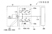
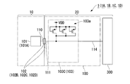
- FIG. 3 is a schematic circuit diagram showing a circuit example (first example) including the electrostatic protection circuit of the solid-state imaging device according to the first embodiment of the present invention.
- FIG. 6 is a schematic circuit diagram showing a circuit example (second example) including the electrostatic protection circuit of the solid-state imaging device according to the first embodiment of the present invention.
- FIG. 6 is a schematic circuit diagram showing a circuit example (third example) including the electrostatic protection circuit of the solid-state imaging device according to the first embodiment of the present invention.
- FIG. 6 is a schematic circuit diagram showing a circuit example (fourth example) including the electrostatic protection circuit of the solid-state imaging device according to the first embodiment of the present invention.
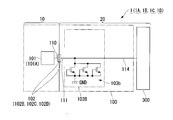
- FIG. 6 is a schematic circuit diagram showing a circuit example (fifth example) including the electrostatic protection circuit of the solid-state imaging device according to the first embodiment of the present invention.
- FIG. 1 is a schematic diagram showing the configuration of an imaging system according to a first embodiment of the present invention.
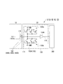
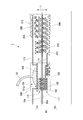
- FIG. 2 is a schematic cross-sectional view showing a configuration example of the solid-state imaging device according to the first embodiment of the present invention.
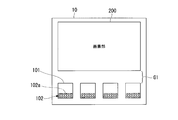
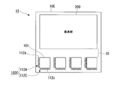
- FIG. 3A is a schematic plan view showing the configuration of the first substrate of the solid-state imaging device according to the first embodiment of the present invention.
- FIG. 3B is a schematic plan view showing the configuration of the second substrate of the solid-state imaging device according to the first embodiment of the present invention.
- Each drawing is a schematic view, and the size and shape of each part are exaggerated (the same applies to the following drawings).
- an imaging system 8 of the present embodiment includes a lens unit 2, a shutter 7, a solid-state imaging device 1, an image signal processing device 3, a recording device 4, a display device 6, and an imaging control device 5.
- the imaging system 8 can be used in various applications for imaging a subject.
- the imaging system 8 can be used for a digital camera, a digital video camera, an endoscope, a mobile phone having an imaging function, and the like.
- the lens unit 2 condenses the light from the subject.
- the lens unit 2 may be a single lens or may be composed of a plurality of lenses.
- a plurality of lenses are accommodated in a lens barrel.
- the lens unit 2 includes a lens drive mechanism 2a that performs focal position alignment and zooming by changing the arrangement position of the lens.
- the focal position of the lens unit 2 may be fixed. In this case, the lens drive mechanism 2a can be omitted.
- the shutter 7 opens and closes the light path based on the shutter speed and the aperture value set at the time of imaging, and performs exposure on the solid-state imaging device 1 described later.
- the type of the shutter 7 is not particularly limited.
- the shutter 7 may be a mechanical shutter or an electronic shutter.
- an electronic shutter that opens and closes under the control of the imaging control device 5 is an example.
- the shutter 7 can be omitted when configuring a complete electronic shutter.
- the solid-state imaging device 1 of the present embodiment includes a photoelectric conversion element (not shown) for each of the pixels that divide the imaging range. Each photoelectric conversion element receives light which passes through the shutter 7 and reaches the pixel area. Each photoelectric conversion element photoelectrically converts the received light to generate an image signal for each pixel.
- the solid-state imaging device 1 sends an image signal generated by each photoelectric conversion element to an image signal processing device 3 described later. The detailed configuration of the solid-state imaging device 1 will be described later.
- the image signal processing device 3 is electrically connected to the solid-state imaging device 1.
- the image signal processing device 3 subjects the image signal sent from the solid-state imaging device 1 to image processing. Examples of image processing performed by the image signal processing device 3 include noise removal processing, shading correction processing, tone correction processing, and color tone correction processing.
- the image signal processing device 3 is electrically connected to a recording device 4 and a display device 6 described later. The image signal processing device 3 sends the image signal subjected to image processing to the recording device 4 and the display device 6.
- the recording device 4 stores the image signal sent from the image signal processing device 3.
- the type of the recording device 4 is not particularly limited.
- the recording device 4 may be, for example, a memory, a memory card, a hard disk or the like.
- the display device 6 displays the image signal sent from the image signal processing device 3.
- the type of display 6 is not particularly limited.
- the display device 6 may be, for example, a liquid crystal display, an organic EL display, or the like.
- the imaging control device 5 controls the operation of each device portion of the imaging system 8.
- the imaging control device 5 is communicably connected to the lens driving mechanism 2a, the shutter 7, the solid-state imaging device 1, the image signal processing device 3, the recording device 4, the display device 6, and an operation unit (not shown).
- the example of the control which the imaging control apparatus 5 in this embodiment performs is as follows.
- the imaging control device 5 performs focus alignment of the lens unit 2 based on the image captured by the solid-state imaging device 1.
- the imaging control device 5 controls the operation of the shutter 7 to perform exposure control.
- the imaging control device 5 can change the image processing of the image signal processing device 3 according to the operation input from the operation unit (not shown).
- the imaging control device 5 switches the display mode of the display device 6 according to the operation input from the operation unit (not shown).
- a display mode of the display device 6 for example, a mode for displaying a still image to be captured, a mode for displaying a moving image to be captured, a mode for reproducing an image stored in the recording device 4, a mode for displaying an operation menu, etc. Can be mentioned.
- the solid-state imaging device 1 includes a first substrate 10 and a second substrate 20.
- the first substrate 10 and the second substrate 20 are stacked on one another in the stacking direction L to constitute a solid-state imaging device main body 50.
- the first substrate 10 and the second substrate 20 are bonded to each other in a state in which the facing surfaces 10a and 20a facing each other are in contact with each other.
- the external shapes of the first substrate 10 and the second substrate 20 are desirably rectangular as shown in FIGS. 3A and 3B, but the external shapes may be different.
- the first substrate 10 includes an electrode pad 101 (electrode unit), a wiring unit 110, and a pixel unit 200.
- the electrode pad 101 is formed of a metal layer formed on the first substrate 10.
- a hole 10 b is formed to penetrate the semiconductor forming layer such as Si (silicon) up to the surface of the electrode pad 101.
- the size of the hole 10 b is smaller than the area of the surface of the electrode pad 101 where the holes 10 b overlap. Therefore, the connection surface 101a which is the surface of the electrode pad 101 is exposed inside the hole 10b.
- the connection surface 101 a can be electrically connected by contact or bonding with an appropriate metal from the outside of the solid-state imaging device 1.
- the electrode pad 101 constitutes an electrode portion having a connection surface provided so as to be electrically connectable to the outside of the first substrate 10. Although appropriate wires are connected to the electrode pads 101 in order to be electrically connected to the outside of the first substrate 10, illustration thereof is omitted in FIG.
- the outer shape of the electrode pad 101 and the outer shape of the connection surface 101a are not particularly limited.
- the outer shape of the electrode pad 101 and the connection surface 101a may be, for example, a polygon, a circle, or an ellipse.
- the electrode pad 101 and the connection surface 101a are both rectangular.
- a wiring portion 110 connected to the electrode pad 101 is formed on the first substrate 10 closer to the facing surface 10 a than the electrode pad 101.
- the wiring portions 110 extend in the stacking direction L as a whole, for example, by alternately arranging metal layers and vias electrically connected to each other.
- the wiring portion 110 is connected to a first substrate connection portion 102, which will be described later, disposed between the facing surfaces 10a and 20a.
- the wiring portion 110 electrically connects the electrode pad 101 and the first substrate connection portion 102.
- the pixel unit 200 photoelectrically converts incident light according to the amount of light, generates a signal based on charge, and includes a plurality of photoelectric conversion elements 201.
- the pixel unit 200 is formed on the first substrate 10 using a semiconductor manufacturing process.
- the photoelectric conversion element 201 for example, a photodiode element can be mentioned.
- the area in which the pixel unit 200 is formed (hereinafter referred to as the area of the pixel unit 200) has a rectangular shape located inside the first substrate 10 as schematically shown in FIG. 3A when viewed from the stacking direction L .
- Each outer edge portion of the region of the pixel unit 200 is substantially parallel (including parallel) to the outer shape of the first substrate 10 that each faces.
- a band-like region is formed on the outer side of the pixel unit 200 with the outer edge of the first substrate 10. These band-like regions can form the electrode pad 101 in any region.
- the electrode pad 101 may be disposed over four regions facing the four sides of the region of the pixel unit 200.
- the electrode pad 101 may be disposed across two regions facing two sides of the region of the pixel unit 200. In FIG.
- the plurality of electrode pads 101 are illustrated only in one band-like region sandwiched between one long side of the region of the pixel unit 200 and the outer shape of the first substrate 10. Furthermore, the number of electrode pads 101 shown in FIG. 3A is also an example. The number of electrode pads 101 is not limited to four, and may be three or less, or five or more. Each electrode pad 101 does not overlap with the pixel unit 200, and when viewed in the stacking direction L, the pixel unit 200 and each electrode pad 101 are opposed to each other across the region G1.
- the photoelectric conversion elements 201 are arranged at fixed pitches in two directions parallel to the outer shape of the area of the pixel section 200 when viewed in the stacking direction L. Therefore, the pixel unit 200 is divided into a plurality of pixels corresponding to each photoelectric conversion element 201 as viewed in the stacking direction L.
- a microlens portion 113 formed of transparent resin is disposed for each pixel of the pixel portion 200.
- the microlens unit 113 condenses incident light from the outside on the photoelectric conversion element 201 to which the microlens unit 113 faces.
- a color filter such as red, green, or blue may be formed between the micro lens unit 113 and the photoelectric conversion element 201.
- the second substrate 20 includes a peripheral circuit unit 300 (peripheral circuit), a wiring unit 111, and an electrostatic protection circuit 103.
- Peripheral circuit unit 300 includes a read circuit and a control circuit.
- the peripheral circuit unit 300 is formed on the second substrate 20 using a semiconductor manufacturing process.
- the readout circuit of the peripheral circuit unit 300 reads out a signal based on the charge of each photoelectric conversion element 201 in the pixel unit 200.
- the control circuit of the peripheral circuit unit 300 controls the read timing of the read out circuit, and outputs the signal read from each photoelectric conversion element 201 as an image signal corresponding to the arrangement position of the photoelectric conversion element 201.
- the region in which the peripheral circuit portion 300 is formed (hereinafter referred to as the region of the peripheral circuit portion 300) is a rectangular shape located inside the second substrate 20 as schematically shown in FIG. 3B when viewed from the stacking direction L. It is.
- Each outer edge portion of the region of the peripheral circuit portion 300 is substantially parallel (including parallel) to the outer shape of the second substrate 20 to which it faces.
- a band-shaped region is formed on the outer side of the peripheral circuit portion 300 with the outer edge of the second substrate 20. When viewed in the stacking direction L, the band-like region of the second substrate 20 at least overlaps the region of the first substrate 10 where the electrode pad 101 is formed.
- the area of the area of the peripheral circuit unit 300 is larger than the area of the area of the pixel unit 200.
- the peripheral circuit portion 300 and the electrode pad 101 do not overlap.
- the peripheral circuit unit 300 and each electrode pad 101 are opposed to each other across the region G2.
- the width of the region G2 in the opposing direction to the peripheral circuit portion 300 and each electrode pad 101 viewed from the stacking direction L is narrower than the width of the region G1 in the opposing direction to the pixel portion 200 and each electrode pad 101. But it is not necessarily the case.
- the peripheral circuit unit 300 is electrically connected to the pixel unit 200 and the electrode pad 101 in the first substrate 10. As shown in FIG. 2, in order to make such an electrical connection, a first substrate connection portion 102 (a substrate connection portion connected to an electrode portion) is disposed between the first substrate 10 and the second substrate 20. The second substrate connection portion 115 is disposed inside the second substrate 20.
- the first substrate connection portion 102 applies pressure to the connection electrode formed on the opposing surface 10 a and the connection electrode formed on the opposing surface 20 a through, for example, a connection metal material such as a micro bump or a fine electrode. It is formed by The number of connection electrodes in the first substrate connection portion 102 may be one or more for each electrode pad 101 to be connected. In the present embodiment, when viewed from the stacking direction L, the first substrate connection portion 102 for one electrode pad 101 has a plurality of connection electrodes arranged in a rectangular area. However, since FIG. 2, FIG. 3A, and FIG. 3B are schematic diagrams, the number of connection electrodes does not correspond exactly between FIG. 2, FIG. 3A, and FIG. 3B.
- the first substrate connection portion 102 is the connection electrodes formed on the facing surfaces 10a and 20a and the connection material sandwiched therebetween.
- the first substrate connection portion is represented in a case where a circumscribed polygon region (indicated by a two-dot chain line in the drawing) including all the connection electrodes constituting one first substrate connection portion 102 is represented. It may be called a formation region of 102.
- the formation region 102a of the first substrate connection portion 102 in this embodiment has a rectangular shape as an example.
- connection electrode formed on the facing surface 10 a of the first substrate connection portion 102 is connected to the electrode pad 101 via the wiring portion 110.
- the first substrate connection portion 102 is a substrate connection portion connected to the electrode pad 101.
- the formation region 102a of the first substrate connection portion 102 is narrower than the area of the electrode pad 101 to which the first substrate connection portion 102 is connected.
- the formation region 102 a of each first substrate connection portion 102 overlaps the inside of the electrode pad 101 to which it is connected. For this reason, the first substrate connection portion 102 itself also overlaps the inside of the electrode pad 101.
- the first substrate connection portion 102 is disposed below the electrode pad 101 so as to be away from the pixel portion 200 and the peripheral circuit portion 300.
- the electrode pad 101 overlaps with the first substrate connection portion 102 and the pixel portion 200 and the peripheral circuit portion 300, and overlaps with the formation region 102a of the first substrate connection portion 102. Areas are formed.
- the solid-state imaging device 1 is an example in which the first substrate connecting portion 102 does not overlap the region G2 when viewed in the stacking direction L. That is, the first substrate connection portion 102 is disposed at a position excluding the region G2 which is a region sandwiched between the electrode pad 101 and the peripheral circuit portion 300.
- the second substrate connection unit 115 has the same configuration as the first substrate connection unit 102. However, the second substrate connection portion 115 electrically connects the peripheral circuit portion 300 and the pixel portion 200 through appropriate wirings or circuits.
- the second substrate connection portion 115 is disposed in a region not overlapping the electrode pad 101 when viewed in the stacking direction L.
- the second substrate connection portion 115 may be disposed, for example, in a region overlapping with the pixel portion 200 or the peripheral circuit portion 300 when viewed in the stacking direction L.
- the second substrate connection portion 115 may be disposed, for example, in a region not overlapping the electrode pad 101 outside the pixel portion 200 or the peripheral circuit portion 300 when viewed in the stacking direction L. In the case of the second substrate connection portion 115 illustrated in FIG.
- the second substrate connection portion 115 is located in an area outside the pixel portion 200 and inside the peripheral circuit portion 300 when viewed in the stacking direction L. It is arranged.
- the second substrate connection portion 115 can be provided according to the need for wiring, and the number is not particularly limited.
- the wiring portion 111 is connected to the connection electrode formed on the facing surface 20 a in the first substrate connection portion 102.
- the wiring portion 111 is connected to the peripheral circuit portion 300 directly or indirectly via a circuit.
- the wiring portion 111 electrically connects the first substrate connection portion 102 and the peripheral circuit portion 300.
- the wiring portion 111 extends in the stacking direction L in a region overlapping with the formation region of the first substrate connection portion 102 when viewed in the stacking direction L, and then extends toward the peripheral circuit portion 300 inside the second substrate 20.
- the wiring portion 111 is, for example, alternately arranged with metal layers and vias electrically connected to each other, similarly to the wiring portion 110.
- the wiring portion 111 extends toward the peripheral circuit portion 300 by any metal layer constituting the wiring portion 111.
- the electrostatic protection circuit 103 protects the peripheral circuit unit 300 and the pixel unit 200 from the STD generated through the electrode pad 101. Therefore, the electrostatic protection circuit 103 is connected to the circuit between the first substrate connection portion 102 and the peripheral circuit portion 300 in the second substrate 20.
- the electrostatic protection circuit 103 is disposed in a region not overlapping any of the first substrate connection portion 102 and the second substrate connection portion 115 when viewed in the stacking direction L.
- not overlapping with the first substrate connection portion 102 and the second substrate connection portion 115 means that when viewed in the stacking direction L, any connection electrodes do not overlap.
- the electrostatic protection circuit 103 overlaps the electrode pad 101 when viewed in the stacking direction L, and the formation region 102a of the first substrate connection portion 102. It is arranged in the area which does not overlap.
- the electrode pad 101, the wiring portion 110, the first substrate connection portion 102, the wiring portion 111, and the electrostatic protection circuit 103 perform input / output between the solid-state imaging device 1 and the outside. Configure a part.
- the circuit configuration of the electrostatic protection circuit 103 may be different depending on the type of input / output at each electrode pad 101.
- the IO unit 100 can include circuit elements other than the above depending on the type of input / output at each electrode pad 101.
- FIG. 4 to 8 are schematic circuit diagrams showing circuit examples (first to fifth examples) including the electrostatic protection circuit of the solid-state imaging device according to the first embodiment of the present invention.
- FIG. 9 is a schematic cross-sectional view showing a configuration example of the wiring state of the solid-state imaging device according to the first embodiment of the present invention.
- the circuit example (first example) shown in FIG. 4 is an example where the electrode pad 101 is a digital input terminal.
- the IO unit 100 of the first example includes an electrode pad 101, a wiring unit 110, a first substrate connection unit 102, a wiring unit 111, an electrostatic protection circuit 103A, and a driver circuit 104A.
- the wiring portion 111 electrically connects the first substrate connection portion 102 and the driver circuit 104A.
- FIG. 4 shows only the main circuit elements of the IO unit 100 for the schematic view. In addition to the illustrated circuit elements, for example, appropriate circuit elements such as resistors may be provided (the same applies to FIGS. 5 to 8).
- the electrostatic protection circuit 103A of the first example includes a first protection circuit 103a in which a plurality of NMOS transistors are diode-connected and a second protection circuit 103b in which a plurality of PMOS transistors is diode-connected.
- the number of elements in the first protection circuit 103a and the second protection circuit 103b can be appropriately set according to the current capacity required for electrostatic protection.
- the source and gate of each NMOS transistor are connected to the power supply line of the constant voltage VDD, and the drain is connected to the wiring portion 111.
- the source and gate of each PMOS transistor of the second protection circuit 103 b are connected to the ground (GND) line, and the drain is connected to the wiring portion 111.
- the input port is connected to the wiring portion 111, and the output port is connected to the peripheral circuit portion 300 via the wiring portion 114. Therefore, the driver circuit 104A inputs the digital signal input to the electrode pad 101 to the peripheral circuit unit 300.
- the IO unit 100 of the first example when the electric signal input to the electrode pad 101 is 0 V or more and VDD or less, current does not flow in the first protection circuit 103 a and the second protection circuit 103 b. However, when an excessive voltage is applied to the electrode pad 101 by STD or the like, a current flows in the first protective circuit 103a or the second protective circuit 103b, and the excessive current is released to the power supply line or the ground line. Therefore, even if STD is input to the electrode pad 101, the driver circuit 104A and the peripheral circuit portion 300 can be prevented from being damaged.
- the first protection circuit 103a and the second protection circuit 103b function, for example, even in a state in which the solid-state imaging device is not incorporated in the imaging system (a state in which each voltage is not input to the electrode pad 101 of the solid-state imaging device). That is, regardless of the potentials of the power supply line and the ground line, when an excessive voltage is applied to the electrode pad 101 by STD or the like, an excessive current is caused to flow to the power supply line or the ground line, and a failure of the driver circuit 104A or the peripheral circuit portion 300. To prevent.
- the circuit example (second example) shown in FIG. 5 is an example where the electrode pad 101 is a digital output terminal.
- the IO unit 100 of the second example includes an electrode pad 101, a wiring unit 110, a first substrate connection unit 102, a wiring unit 111, an electrostatic protection circuit 103A, and a driver circuit 104B.
- the wiring portion 111 electrically connects the first substrate connection portion 102 and the driver circuit 104B.
- the driver circuit 104 B has an input port connected to the peripheral circuit unit 300 via the wiring unit 114, and an output port connected to the wiring unit 111. Therefore, the driver circuit 104B outputs the digital signal sent from the peripheral circuit unit 300 to the electrode pad 101.
- the IO unit 100 of the second example no current flows in the first protection circuit 103a and the second protection circuit 103b when the driver circuit 104B outputs a digital signal.
- a current flows in the first protective circuit 103a or the second protective circuit 103b, and the excessive current is released to the power supply line or the ground line. Therefore, even if STD is input to the electrode pad 101, failure of the driver circuit 104B and the peripheral circuit portion 300 can be prevented.
- the circuit example (third example) shown in FIG. 6 is an example where the electrode pad 101 is an analog terminal.
- the IO unit 100 of the third example includes an electrode pad 101, a wiring unit 110, a first substrate connection unit 102, a wiring unit 111, and an electrostatic protection circuit 103A.
- the wiring portion 111 is electrically connected to the peripheral circuit portion 300 via the wiring portion 114.
- This example is an example in which the driver circuit 104A is deleted in the first example. Therefore, the electrode pad 101 can be used as an analog input terminal for inputting an electric signal input from the outside to the peripheral circuit unit 300 as it is, or an analog output terminal for outputting an output signal from the peripheral circuit unit 300 to the outside as it is it can.
- the IO unit 100 of the third example when the input / output voltage at the electrode pad 101 is 0 V or more and VDD or less, no current flows in the first protection circuit 103 a and the second protection circuit 103 b. However, when an excessive voltage is externally applied to the electrode pad 101 by STD or the like, a current flows in the first protective circuit 103a or the second protective circuit 103b, and the excessive current is released to the power supply line or the ground line. For this reason, even if STD is input to the electrode pad 101, a failure of the peripheral circuit unit 300 can be prevented.
- the circuit example (fourth example) shown in FIG. 7 is an example in the case where the electrode pad 101 is a power supply terminal.
- the IO unit 100 of the fourth example includes an electrode pad 101, a wiring unit 110, a first substrate connection unit 102, a wiring unit 111, and an electrostatic protection circuit 103B.
- the wiring portion 111 is electrically connected to the peripheral circuit portion 300 via the wiring portion 114.
- the electrostatic protection circuit 103A is replaced with the electrostatic protection circuit 103B in the first example, and the driver circuit 104A is eliminated.
- the electrostatic protection circuit 103B is configured by deleting the first protection circuit 103a from the electrostatic protection circuit 103A of the first example.
- the IO unit 100 of the fourth example when the voltage of VDD is applied to the electrode pad 101, no current flows in the second protection circuit 103b. However, when an excessive voltage is externally applied to the electrode pad 101 by STD or the like, a current flows in the second protection circuit 103b, and the excessive current is released to the ground line. For this reason, even if STD is input to the electrode pad 101, a failure of the peripheral circuit unit 300 can be prevented.
- the circuit example (fifth example) shown in FIG. 8 is an example where the electrode pad 101 is a ground terminal.
- the IO unit 100 of the fifth example includes an electrode pad 101, a wiring unit 110, a first substrate connection unit 102, a wiring unit 111, and an electrostatic protection circuit 103C.
- the wiring portion 111 is electrically connected to the peripheral circuit portion 300 via the wiring portion 114.
- This example is an example in which the electrostatic protection circuit 103C is provided instead of the electrostatic protection circuit 103A in the first example, and the driver circuit 104A is eliminated.
- the electrostatic protection circuit 103C is configured by deleting the second protection circuit 103b from the electrostatic protection circuit 103A of the first example.
- the IO unit 100 of the fourth example when the electrode pad 101 is at the same potential as the ground, no current flows in the first protection circuit 103a. However, when an excessive voltage is applied to the electrode pad 101 from the outside by STD or the like, a current flows in the first protection circuit 103 a and the excessive current is released to the power supply line. For this reason, even if STD is input to the electrode pad 101, a failure of the peripheral circuit unit 300 can be prevented.
- Each example of the IO unit 100 described above can be mixed and used in the solid-state imaging device 1 according to the type of input / output at the electrode pad 101.
- the first substrate 10 and the second substrate 20 are manufactured by a semiconductor manufacturing process.
- the opposing surface 10 a of the first substrate 10 and the opposing surface 20 a of the second substrate 20 are opposed to each other, and connection is made between the connection electrodes of the first substrate connection portion 102 and the second substrate connection portion 115. Arrange the materials and stack them.
- the first substrate 10 and the second substrate 20 are pressurized in the stacking direction L. Thereby, the connection electrodes and the opposing surfaces 10a and 20a opposed to each other are in close contact and joined. Furthermore, the connection electrodes are also electrically connected to each other by the connection material.
- the solid-state imaging device main body 50 is manufactured.
- the solid-state imaging device main body 50 is connected to, for example, another chip constituting another circuit or a lead provided in a package of the solid-state imaging device 1 using, for example, wire bonding or the like.
- the solid-state imaging device 1 is manufactured.
- FIG. 9 shows an example in which the electrode pad 101 is wire-bonded.
- the bonding wire 30 is connected to the electrode pad 101 at the connection surface 101 a.
- Connection surface 101a after wire bonding has a portion exposed to the outside and a portion covered by bonding wire 30 exposed to the outside. Therefore, the electrode pad 101 is electrically susceptible to external STD. Furthermore, in this state, the connection surface 101a and the bonding wire 30 may be charged to generate STD.
- the electrostatic protection circuit 103 provided for each electrode pad 101 overlaps the electrode pad 101 when viewed from the stacking direction L, and the first substrate connection portion 102 and the first substrate connection portion 102 It is formed in a region which does not overlap with the second substrate connection portion 115.
- the electrostatic protection circuit 103 is formed within the formation range of the electrode pad 101 which requires a certain area for connection.
- the sizes of the first substrate 10 and the second substrate 20 can be reduced as compared with the case where the electrostatic protection circuit 103 is disposed in a region not overlapping the electrode pad 101.
- the electrostatic protection circuit 103 does not overlap the first substrate connection portion 102 and the second substrate connection portion 115 when viewed in the stacking direction L, pressure is applied when the first substrate 10 and the second substrate 20 are bonded. During the process, it is less susceptible to the stress generated from the first substrate connection portion 102.
- the electrostatic protection circuit 103 when the electrical characteristics of circuit elements such as a transistor and a diode that constitute the electrostatic protection circuit 103 change from design values, the STD resistance may change significantly. However, according to the present embodiment, when the first substrate 10 and the second substrate 20 are bonded, no excessive stress is applied to the electrostatic protection circuit 103.
- the electrostatic protection circuit 103 of the solid-state imaging device 1 can maintain good STD resistance even after the first substrate 10 and the second substrate 20 are bonded.
- the solid-state imaging device 1 can use a connecting material such as a bump that easily generates stress due to pressure when bonding the first substrate 10 and the second substrate 20, so that bonding can be performed inexpensively and rapidly. Since the solid-state imaging device 1 does not need to reduce the pressing force in consideration of the influence on the electrostatic protection circuit 103 when the first substrate 10 and the second substrate 20 are bonded, the reliability of the bonding can also be improved. . Furthermore, when the solid-state imaging device main body 50 is fixed or wired after the first substrate 10 and the second substrate 20 are joined, the solid-state imaging device main body 50 may be pressurized in the stacking direction L. Also in this case, according to the configuration of the solid-state imaging device 1, the change in the STD resistance of the electrostatic protection circuit 103 can be suppressed.
- a connecting material such as a bump that easily generates stress due to pressure when bonding the first substrate 10 and the second substrate 20, so that bonding can be performed inexpensively and rapidly. Since the solid-state imaging device 1 does not need to reduce the pressing force
- the first substrate connecting portion 102 when viewed from the stacking direction L, the first substrate connecting portion 102 is disposed at a position not overlapping the region G2. Therefore, an increase in chip area can be suppressed without the area of the peripheral circuit portion or the pixel portion being compressed by the substrate connection portion.
- the solid-state imaging device 1 even if the substrate size is compact, it is possible to suppress a change in electrostatic discharge resistance at the time of substrate bonding.
- FIG. 10 is a schematic cross-sectional view showing a configuration example of a solid-state imaging device according to a second embodiment of the present invention.
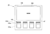
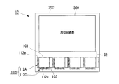
- FIG. 11A is a schematic plan view showing the configuration of the first substrate of the solid-state imaging device according to the second embodiment of the present invention.
- FIG. 11B is a schematic plan view showing the configuration of the second substrate of the solid-state imaging device according to the second embodiment of the present invention.
- the solid-state imaging device 1A of the present embodiment can be used in place of the solid-state imaging device 1 in the imaging system 8 of the first embodiment.
- a solid-state imaging device 1A includes a first substrate 10A and a second substrate 20A instead of the first substrate 10 and the second substrate 20 of the solid-state imaging device 1 of the first embodiment.
- the first substrate 10A includes an electrode pad 101A (electrode portion) in which the electrode pad 101 of the first embodiment is extended more toward the pixel portion 200, instead of the electrode pad 101.
- the area and the arrangement position of the connection surface 101 a are the same as those of the first substrate 10. Therefore, as shown in FIG. 11A, a region g1 narrower than the region G1 is formed between the pixel unit 200 and the electrode pad 101A.
- the wiring portion 110 and the first substrate connection portion 102 in the first substrate 10A overlap the electrode pads 101A on the pixel portion 200 side with respect to the connection surface 101a. Placed in the area. That is, the wiring portion 110 and the first substrate connection portion 102 are not disposed between the connection surface 101 a and the facing surface 10 a.
- the second substrate 20A is moved to a position where the position of the wiring portion 111 overlaps the formation region 102a of the first substrate connection portion 102 when viewed in the stacking direction L.
- the wiring portion 111 (see FIG. 10) is extended in a direction away from the peripheral circuit portion 300 from the region overlapping the wiring portion 111 to electrostatically protect the region overlapping the connection surface 101a. It is connected to the circuit 103.
- the electrode pad 101A, the wiring portion 110, the first substrate connection portion 102, the wiring portion 111, and the electrostatic protection circuit 103 are parts of the IO portion 100 as in the first embodiment.
- Configure see Figure 4
- the configurations of all the IO units 100 and the electrostatic protection circuit 103 described in the first embodiment can be adopted in the solid-state imaging device 1A (see FIGS. 5 to 8).
- the solid-state imaging device 1A can be manufactured in exactly the same manner only by replacing the first substrate 10 and the second substrate 20 in the first embodiment with the first substrate 10A and the second substrate 20A. However, on the opposing surfaces 10a and 20a of the first substrate 10A and the second substrate 20A, the connection electrodes of the first substrate connection portion 102 corresponding to the position of the first substrate connection portion 102 described above in the present embodiment. Is formed.
- the electrostatic protection circuit 103 when viewed in the stacking direction L, the electrostatic protection circuit 103 is disposed in a region overlapping with the electrode pad 101A, and the electrostatic protection circuit 103 does not overlap with the first substrate connection portion 102. Therefore, even in the present embodiment, as in the first embodiment, even if the substrate size is compact, it is possible to suppress a change in electrostatic discharge resistance at the time of substrate bonding.
- the first substrate connection portion 102 when viewed in the stacking direction L, the first substrate connection portion 102 is formed in a region not overlapping the connection surface 101 a. Therefore, when bonding wire 30 is bonded to electrode pad 101A, a load such as pressure or stress transmitted through connection surface 101a is not easily transmitted to first substrate connection portion 102. As a result, the load received by the first substrate connection portion 102 at the time of wire bonding is reduced, so that the connection reliability in the first substrate connection portion 102 is improved.
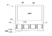
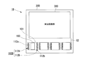
- FIG. 12A is a schematic plan view showing the configuration of the first substrate of the solid-state imaging device according to the third embodiment of the present invention.
- FIG. 12B is a schematic plan view showing the configuration of the second substrate of the solid-state imaging device according to the third embodiment of the present invention.
- the solid-state imaging device 1B of this embodiment can be used in place of the solid-state imaging device 1 in the imaging system 8 of the first embodiment.
- a sectional view is not shown, the solid-state imaging device 1B is replaced with a first substrate 10B (see FIG. 12A) and a second substrate 20B (in place of the first substrate 10 and the second substrate 20 in the first embodiment). (See FIG. 12B).
- first substrate 10B see FIG. 12A
- second substrate 20B in place of the first substrate 10 and the second substrate 20 in the first embodiment.
- the first substrate 10B and the second substrate 20B of the solid-state imaging device 1B are disposed between the first substrate 10B and the second substrate 20B instead of the first substrate connection portion 102.
- the first substrate connection portion 102B substrate connection portion connected to the electrode portion.
- the first substrate connection portion 102B includes a first connection portion 112A and a second connection portion 112B in the vicinity of the outer edge portion of each electrode pad 101 in the direction in which each electrode pad 101 faces.
- the first connection portion 112A is located near the side surface on the left side in the drawing, and the second connection portion 112B is located near the side surface on the right side in the drawing.
- Both the formation region 112 a of the first connection portion 112 A and the formation region 112 b of the second connection portion 112 B have a rectangular shape parallel to the outer edge portion of the electrode pad 101.
- the first connection portion 112A and the second connection portion 112B are located in a region (outside the electrode pad 101) that does not overlap with the electrode pad 101.
- the first connection portion 112A and the second connection portion 112B are located in a region not overlapping any of the regions G1 and G2.
- the wiring portion 110 when viewed in the stacking direction L, is formed in a range covering the electrode pad 101, the first connection portion 112A, and the second connection portion 112B.
- the wiring portion 111 is formed in a range covering the electrode pad 101, the first connection portion 112A, and the second connection portion 112B.
- the electrostatic protection circuit 103 in the present embodiment overlaps the electrode pad 101 when viewed in the stacking direction L in the second substrate 20B, and extends substantially parallel (including parallel) to the formation regions 112a and 112b. Be placed.
- the electrostatic protection circuit 103 is disposed at a position approximately equidistant (including the case of equidistant) from the adjacent formation regions 112a and 112b.
- the electrostatic protection circuit 103 is electrically connected to the wiring portion 111 (not shown).
- the electrode pad 101, the wiring portion 110, the first substrate connection portion 102B, the wiring portion 111, and the electrostatic protection circuit 103 are parts of the IO portion 100 as in the first embodiment.
- Configure see Figure 4
- the configurations of all the IO units 100 and the electrostatic protection circuit 103 described in the first embodiment can be adopted in the solid-state imaging device 1B (see FIGS. 5 to 8).
- the solid-state imaging device 1B can be manufactured in exactly the same manner only by replacing the first substrate 10 and the second substrate 20 of the first embodiment with the first substrate 10B and the second substrate 20B. However, on the facing surfaces 10a and 20a (not shown) of the first substrate 10B and the second substrate 20B, the connection electrodes of the first substrate connecting portion 102B corresponding to the position of the first substrate connecting portion 102B described above Is formed.
- the electrostatic protection circuit 103 when viewed in the stacking direction L, the electrostatic protection circuit 103 is disposed in a region overlapping the electrode pad 101 and a region not overlapping the first substrate connection portion 102B. Therefore, even in the present embodiment, as in the first embodiment, even if the substrate size is compact, it is possible to suppress a change in electrostatic discharge resistance at the time of substrate bonding.
- the first substrate connection portion 102B is disposed at a position not overlapping the region G2 when viewed from the stacking direction L, similarly to the first substrate connection portion 102 of the first embodiment. . Therefore, as in the first embodiment, the increase in the chip area can be suppressed without the area of the peripheral circuit portion or the pixel portion being compressed by the substrate connection portion.
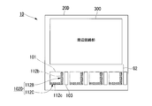
- FIG. 13A is a schematic plan view showing the configuration of the first substrate of the solid-state imaging device according to the fourth embodiment of the present invention.
- FIG. 13B is a schematic plan view showing the configuration of the second substrate of the solid-state imaging device according to the fourth embodiment of the present invention.
- the solid-state imaging device 1C of this embodiment can be used in place of the solid-state imaging device 1 in the imaging system 8 of the first embodiment.
- a sectional view is not shown, the solid-state imaging device 1C is replaced with a first substrate 10C (see FIG. 13A) and a second substrate 20C (in place of the first substrate 10 and the second substrate 20 in the first embodiment). (See FIG. 13B).
- first substrate 10C see FIG. 13A
- second substrate 20C in place of the first substrate 10 and the second substrate 20 in the first embodiment.
- the first substrate 10C and the second substrate 20C of the solid-state imaging device 1C are disposed between the first substrate 10C and the second substrate 20C instead of the first substrate connection portion 102.
- the first substrate connection portion 102C includes a first connection portion 112A and a third connection portion 112C similar to those in the third embodiment.
- the third connection portion 112 ⁇ / b> C is located in the vicinity of an outer edge portion opposite to the outer edge portion facing the pixel portion 200 in each electrode pad 101.
- the third connection portion 112C faces the pixel portion 200 with the electrode pad 101 interposed therebetween.
- the formation region 112 c of the third connection portion 112 ⁇ / b> C has a rectangular shape parallel to the outer edge portion of the electrode pad 101.
- the third connection portion 112 ⁇ / b> C is located in a region (outside of the electrode pad 101) that does not overlap with the electrode pad 101 when viewed in the stacking direction L. For this reason, in the present embodiment, when viewed in the stacking direction L, the first connection portion 112A and the third connection portion 112C are located in a region not overlapping any of the regions G1 and G2.
- the wiring portion 110 when viewed in the stacking direction L, is formed in a range covering the electrode pad 101, the first connection portion 112A, and the third connection portion 112C.
- the wiring portion 111 is formed in a range covering the electrode pad 101, the first connection portion 112A, and the third connection portion 112C.
- the electrostatic protection circuit 103 in the present embodiment is an electrode pad in the vicinity of the outer edge portion of the electrode pad 101 on the opposite side to the first connection portion 112A when viewed in the stacking direction L in the second substrate 20C. It is arrange
- the electrode pad 101, the wiring portion 110, the first substrate connection portion 102C, the wiring portion 111, and the electrostatic protection circuit 103 are parts of the IO portion 100 as in the first embodiment.
- Configure see Figure 4
- the configurations of all the IO units 100 and the electrostatic protection circuit 103 described in the first embodiment can be adopted in the solid-state imaging device 1C (see FIGS. 5 to 8).
- the solid-state imaging device 1C can be manufactured in exactly the same manner only by replacing the first substrate 10 and the second substrate 20 of the first embodiment with the first substrate 10C and the second substrate 20C. However, on the facing surfaces 10a and 20a (not shown) of the first substrate 10C and the second substrate 20C, the connection electrodes of the first substrate connecting portion 102C corresponding to the position of the first substrate connecting portion 102C described above Is formed.
- the electrostatic protection circuit 103 when viewed in the stacking direction L, the electrostatic protection circuit 103 is disposed in a region not overlapping the first substrate connection portion 102C. For this reason, also in the present embodiment, it is possible to suppress a change in electrostatic discharge resistance at the time of bonding the substrates, as in the first embodiment.
- the electrostatic protection circuit 103 is a region on the side of the electrode pad 101 not overlapping the electrode pad 101, and the electrode pads 101 are arranged in the adjacent direction. Adjacent electrode pads 101 need to be spaced to some extent for wiring. For this reason, normally, the space between the adjacent electrode pads 101 is vacant as an area which is not effectively utilized.
- the electrostatic protection circuit 103 since the electrostatic protection circuit 103 is disposed in such an empty space, the electrostatic protection circuit 103 can be disposed without increasing the substrate size by effectively utilizing the empty space. As described above, this embodiment is an example in which the substrate size can be made compact even if the electrostatic protection circuit 103 does not overlap with the electrode pad 101.
- the first substrate connection portion 102C is disposed at a position not overlapping the region G2 when viewed from the stacking direction L, similarly to the first substrate connection portion 102 of the first embodiment. . Therefore, as in the first embodiment, the increase in the chip area can be suppressed without the area of the peripheral circuit portion or the pixel portion being compressed by the substrate connection portion.
- the first substrate connection portion 102C when viewed in the stacking direction L, the first substrate connection portion 102C is formed in a region not overlapping the electrode pad 101 including the connection surface 101a. Therefore, when bonding the bonding wire 30 to the electrode pad 101, a load such as pressure or stress transmitted through the electrode pad 101 is not easily transmitted to the first substrate connection portion 102C. As a result, the load received by the first substrate connection portion 102C is reduced at the time of wire bonding, so that the reliability of connection in the first substrate connection portion 102C is improved.
- FIG. 14A is a schematic plan view showing the configuration of the first substrate of the solid-state imaging device according to the fifth embodiment of the present invention.
- FIG. 14B is a schematic plan view showing the configuration of the second substrate of the solid-state imaging device according to the fifth embodiment of the present invention.
- the solid-state imaging device 1D of the present embodiment can be used in place of the solid-state imaging device 1 in the imaging system 8 of the first embodiment.
- a sectional view is not shown, a solid-state imaging device 1D is replaced with a first substrate 10D (see FIG. 14A) and a second substrate 20D (in place of the first substrate 10 and the second substrate 20 in the first embodiment). (See FIG. 14B).
- first substrate 10D see FIG. 14A
- second substrate 20D in place of the first substrate 10 and the second substrate 20 in the first embodiment.
- the first substrate 10D and the second substrate 20D of the solid-state imaging device 1D are disposed between the first substrate 10C and the second substrate 20C instead of the first substrate connection portion 102.
- the first substrate connection portion 102D includes a third connection portion 112C similar to the fourth embodiment and a second connection portion 112B similar to the third embodiment.
- each of the third connection portion 112C and the second connection portion 112B of the present embodiment is located at a position overlapping the adjacent electrode pad 101 (inside of the electrode pad 101). Be placed.
- the wiring portion 110 is formed in a range covering the electrode pad 101, the second connection portion 112B, and the third connection portion 112C.
- the electrostatic protection circuit 103 in the present embodiment is disposed at the same position as the electrostatic protection circuit 103 in the fourth embodiment.
- the electrostatic protection circuit 103 when viewed in the stacking direction L, is disposed in a region facing the second connection portion 112B and not overlapping the electrode pad 101 and the regions G1 and G2.
- the wiring portion 111 is formed in a range covering the second connection portion 112B, the third connection portion 112C, and the electrostatic protection circuit 103.
- the electrostatic protection circuit 103 is electrically connected to the wiring portion 111 (not shown).
- the electrode pad 101, the wiring portion 110, the first substrate connection portion 102D, the wiring portion 111, and the electrostatic protection circuit 103 are parts of the IO portion 100 as in the first embodiment.
- Configure see Figure 4
- the configurations of all the IO units 100 and the electrostatic protection circuit 103 described in the first embodiment can be adopted in the solid-state imaging device 1D (see FIGS. 5 to 8).
- the solid-state imaging device 1D can be manufactured in exactly the same manner only by replacing the first substrate 10 and the second substrate 20 in the first embodiment with the first substrate 10D and the second substrate 20D.
- the connection electrodes of the first substrate connection portion 102D corresponding to the position of the first substrate connection portion 102D described above. Is formed.
- the electrostatic protection circuit 103 when viewed in the stacking direction L, the electrostatic protection circuit 103 is disposed in a region not overlapping the first substrate connection portion 102D. For this reason, also in the present embodiment, it is possible to suppress a change in electrostatic discharge resistance at the time of bonding the substrates, as in the first embodiment.
- the electrostatic protection circuit 103 is a region on the side of the electrode pad 101 not overlapping the electrode pad 101, and in the direction in which the electrode pads 101 are adjacent. Be placed. Therefore, as in the fourth embodiment, since the electrostatic protection circuit 103 is disposed in the empty space between the electrode pads 101, the electrostatic protection circuit 103 can be effectively utilized to effectively utilize the empty space. Can be placed.
- the first substrate connection portion 102D is disposed at a position not overlapping the region G2 when viewed from the stacking direction L, similarly to the first substrate connection portion 102 of the first embodiment. . Therefore, as in the first embodiment, the increase in the chip area can be suppressed without the area of the peripheral circuit portion or the pixel portion being compressed by the substrate connection portion.
- the first substrate connection portion 102D is formed in a region not overlapping the electrode pad 101 including the connection surface 101a. Therefore, as in the fourth embodiment, the reliability of connection in the first substrate connection portion 102D is improved.
- the second connection portion 112B may be provided instead of the first connection portion 112A.
- the first connection portion 112A may be provided instead of the second connection portion 112B.
- the third connection portion 112C may be deleted.
- the third connection portion 112C may be added to the first substrate connection portion 102B.
- the first substrate connection portion is disposed in the region excluding the regions G 2 and g 2 which is the region sandwiched between the electrode pad 101 and the peripheral circuit portion 300 when viewed in the stacking direction L.
- the first substrate connection portion it is not essential not to arrange the first substrate connection portion in the regions G2 and g2.
- the electrostatic protection circuit 103 when viewed in the stacking direction L, completely overlaps the electrode pad 101 and does not overlap at all. However, as long as the electrostatic protection circuit 103 does not overlap with the first substrate connection portion, only a part thereof may overlap with the electrode pad 101.
Landscapes
- Solid State Image Pick-Up Elements (AREA)
- Engineering & Computer Science (AREA)
- Power Engineering (AREA)
- Transforming Light Signals Into Electric Signals (AREA)
Abstract
固体撮像装置は、光電変換素子が配された第1基板と、第1基板に積層して配置され、光電変換素子の電荷に基づく信号を読み出すための読み出し回路および制御回路を含む周辺回路の少なくとも一部が配された第2基板と、第1基板に設けられ、第1基板の外部に向かって電気的に接続可能に設けられた接続表面を有する電極部と、第1基板と第2基板との間に配置され、第1基板および第2基板とを電気的に接続する基板接続部と、第2基板において、基板接続部のうち電極部に接続された基板接続部と周辺回路との間の回路に接続された静電保護回路と、を備え、第1基板および第2基板が積層される積層方向から見るとき、静電保護回路は、基板接続部のいずれとも重ならない位置に配置されている。
Description
本発明は、固体撮像装置および撮像システムに関する。
従来、半導体基板上に形成された固体撮像装置には、静電保護回路が設けられている。静電保護回路は、ダイオードまたはトランジスタを含んで構成される。静電保護回路は、固体撮像装置の外部に露出する電極部と半導体基板内の電気回路との間の回路に電気的に接続されている。静電保護回路は、電極部のそれぞれに対して設けられている。
固体撮像装置は、例えば、複数の基板が積層され、かつ複数の基板がその間に配される基板接続部によって電気的に接続されて、構成される場合がある。
例えば、特許文献1には、上述したような積層型の固体撮像装置が記載されている。この固体撮像装置は、第1基板に外部に露出するパッド(電極部)が形成される。第1基板に積層される第2基板には、積層時に積層方向から見てパッドと重なる領域に、保護ダイオード回路(静電保護回路)が配される。第1基板と第2基板の間には、積層方向から見てパッド全体と重なる位置に接続部(基板接続部)が配置される。
固体撮像装置は、例えば、複数の基板が積層され、かつ複数の基板がその間に配される基板接続部によって電気的に接続されて、構成される場合がある。
例えば、特許文献1には、上述したような積層型の固体撮像装置が記載されている。この固体撮像装置は、第1基板に外部に露出するパッド(電極部)が形成される。第1基板に積層される第2基板には、積層時に積層方向から見てパッドと重なる領域に、保護ダイオード回路(静電保護回路)が配される。第1基板と第2基板の間には、積層方向から見てパッド全体と重なる位置に接続部(基板接続部)が配置される。
固体撮像装置に含まれる静電保護回路は、良好な静電気放電(STD)耐性を得るために、電流密度の変化に対して敏感に反応するセンシティブな回路である。静電保護回路は、例えば、回路構成が同じでもレイアウトパターン等に起因して回路の電流密度が設計値よりも変化すると、STD耐性が大きく変わる可能性がある。同様に、静電保護回路を構成する回路素子の電気特性が設計値から変化しても、STD耐性が大きく変わる可能性がある。
STD耐性が低下すると、固体撮像装置に静電ノイズが混入したり、回路が破損して固体撮像装置の信頼性が低下したりする可能性がある。
STD耐性が低下すると、固体撮像装置に静電ノイズが混入したり、回路が破損して固体撮像装置の信頼性が低下したりする可能性がある。
積層型の固体撮像装置の製造工程では、複数の基板を積層して、基板接続部によって互いに接続する場合に、積層した基板同士に圧力をかける。このとき、各基板内の回路素子が応力を受けるため、回路素子の電気特性が変化する場合がある。例えば、回路素子がトランジスタであれば、閾値電圧が変化する場合がある。
基板接続部には、例えば、基板接合用のバンプが配された状態で加圧されるため、その近傍領域の応力が高くなりやすい。
基板接続部には、例えば、基板接合用のバンプが配された状態で加圧されるため、その近傍領域の応力が高くなりやすい。
特許文献1に記載の積層型の固体撮像装置は、積層方向から見て、接続部と重なる領域に保護ダイオード回路が配されている。このため、保護ダイオード回路は、第1基板および第2基板の接合時に、応力を受けやすい。
したがって、特許文献1に記載の積層型の固体撮像装置は、基板の接合時の圧力によって、保護ダイオード回路のSTD耐性が設計値から変化しやすい。このため、固体撮像装置の信頼性が低下することが懸念される。
したがって、特許文献1に記載の積層型の固体撮像装置は、基板の接合時の圧力によって、保護ダイオード回路のSTD耐性が設計値から変化しやすい。このため、固体撮像装置の信頼性が低下することが懸念される。
本発明は、上記の課題に鑑みてなされたものであり、基板サイズがコンパクトであっても、基板接合時の静電気放電耐性の変化を抑制することができる固体撮像装置および撮像システムを提供することを目的とする。
本発明の第1の態様の固体撮像装置は、光電変換素子が配された第1基板と、前記第1基板に積層して配置され、前記光電変換素子の電荷に基づく信号を読み出すための読み出し回路および制御回路を含む周辺回路の少なくとも一部が配された第2基板と、前記第1基板に設けられ、前記第1基板の外部に向かって電気的に接続可能に設けられた接続表面を有する電極部と、前記第1基板と前記第2基板との間に配置され、前記第1基板および前記第2基板とを電気的に接続する基板接続部と、前記第2基板において、前記基板接続部のうち前記電極部に接続された基板接続部と前記周辺回路との間の回路に接続された静電保護回路と、を備え、前記第1基板および前記第2基板が積層される積層方向から見るとき、前記静電保護回路は、前記基板接続部のいずれとも重ならない位置に配置されている。
本発明の第2の態様によれば、上記第1の態様の固体撮像装置において、前記電極部の面積は、前記電極部に接続された基板接続部の面積より大きく、前記静電保護回路は、前記積層方向から見るとき、前記電極部と重なる位置に配置されてもよい。
本発明の第3の態様によれば、上記第1の態様の固体撮像装置において、前記積層方向から見るとき、前記電極部は、前記周辺回路よりも外側の前記第1基板に配置され、かつ、前記電極部に接続された基板接続部は、前記電極部と前記周辺回路との間に挟まれる領域を除く位置に配置されてもよい。
本発明の第4の態様によれば、上記第3の態様の固体撮像装置において、前記積層方向から見るとき、前記電極部と前記電極部に接続された基板接続部とは、互いに重ならない位置に配置されてもよい。
本発明の第5の態様の撮像システムは、上記第1の態様から第4の態様のいずれか1態様の固体撮像装置を備える。
本発明の固体撮像装置および撮像システムによれば、基板サイズがコンパクトであっても、基板接合時の静電気放電耐性の変化を抑制することができるという効果を奏する。
以下では、本発明の実施形態について添付図面を参照して説明する。すべての図面において、実施形態が異なる場合であっても、同一または相当する部材には同一の符号を付し、共通する説明は省略する。
[第1の実施形態]
本発明の第1の実施形態の固体撮像装置および撮像システムについて説明する。
図1は、本発明の第1の実施形態の撮像システムの構成を示す模式的な構成図である。図2は、本発明の第1の実施形態の固体撮像装置の構成例を示す模式的な断面図である。図3Aは、本発明の第1の実施形態の固体撮像装置の第1基板の構成を示す模式的な平面図である。図3Bは、本発明の第1の実施形態の固体撮像装置の第2基板の構成を示す模式的な平面図である。
各図面は、模式図のため、各部の寸法および形状は誇張されている(以下の図面も同様)。
[第1の実施形態]
本発明の第1の実施形態の固体撮像装置および撮像システムについて説明する。
図1は、本発明の第1の実施形態の撮像システムの構成を示す模式的な構成図である。図2は、本発明の第1の実施形態の固体撮像装置の構成例を示す模式的な断面図である。図3Aは、本発明の第1の実施形態の固体撮像装置の第1基板の構成を示す模式的な平面図である。図3Bは、本発明の第1の実施形態の固体撮像装置の第2基板の構成を示す模式的な平面図である。
各図面は、模式図のため、各部の寸法および形状は誇張されている(以下の図面も同様)。
図1に示すように、本実施形態の撮像システム8は、レンズユニット2、シャッタ7、固体撮像装置1、画像信号処理装置3、記録装置4、表示装置6、および撮像制御装置5を備える。
撮像システム8は、被写体を撮像する種々の用途に用いることができる。例えば、撮像システム8は、デジタルカメラ、デジタルビデオカメラ、内視鏡、撮像機能を有する携帯電話などに用いることができる。
撮像システム8は、被写体を撮像する種々の用途に用いることができる。例えば、撮像システム8は、デジタルカメラ、デジタルビデオカメラ、内視鏡、撮像機能を有する携帯電話などに用いることができる。
レンズユニット2は、被写体からの光を集光する。レンズユニット2は、単レンズでもよいし、複数のレンズから構成されてもよい。本実施形態では、レンズユニット2は、一例として、複数のレンズがレンズ鏡筒に収容されている。
レンズユニット2は、レンズの配置位置を変えて、焦点位置合わせやズーミングを行うレンズ駆動機構2aを備える。ただし、レンズユニット2は、焦点位置が固定されていてもよい。この場合には、レンズ駆動機構2aは省略できる。
レンズユニット2は、レンズの配置位置を変えて、焦点位置合わせやズーミングを行うレンズ駆動機構2aを備える。ただし、レンズユニット2は、焦点位置が固定されていてもよい。この場合には、レンズ駆動機構2aは省略できる。
シャッタ7は、撮像時に設定されるシャッタスピードおよび絞り値に基づいて、光路を開閉して、後述する固体撮像装置1に対する露光を行う。シャッタ7の種類は特に限定されない。例えば、シャッタ7は、機械シャッタでもよいし、電子シャッタでもよい。本実施形態では、一例として、撮像制御装置5の制御によって開閉動作する電子シャッタである。
ただし、固体撮像装置1において、完全な電子式シャッタを構成する場合には、シャッタ7は省略することができる。
ただし、固体撮像装置1において、完全な電子式シャッタを構成する場合には、シャッタ7は省略することができる。
本実施形態の固体撮像装置1は、撮像範囲を分割する画素ごとに、図示略の光電変換素子を備える。各光電変換素子は、シャッタ7を通過して画素領域に到達する光を受光する。各光電変換素子は、受光した光を光電変換して、画素ごとに画像信号を生成する。固体撮像装置1は、各光電変換素子によって生成された画像信号を後述する画像信号処理装置3に送出する。
固体撮像装置1の詳細構成は、後述する。
固体撮像装置1の詳細構成は、後述する。
画像信号処理装置3は、固体撮像装置1と電気的に接続する。画像信号処理装置3は、固体撮像装置1から送出される画像信号に画像処理を施す。
画像信号処理装置3が行う画像処理の例としては、例えば、ノイズ除去処理、シェーディング補正処理、階調補正処理、色調補正処理などを挙げることができる。
画像信号処理装置3は、後述する記録装置4および表示装置6と電気的に接続される。画像信号処理装置3は、画像処理した画像信号を記録装置4および表示装置6に送出する。
画像信号処理装置3が行う画像処理の例としては、例えば、ノイズ除去処理、シェーディング補正処理、階調補正処理、色調補正処理などを挙げることができる。
画像信号処理装置3は、後述する記録装置4および表示装置6と電気的に接続される。画像信号処理装置3は、画像処理した画像信号を記録装置4および表示装置6に送出する。
記録装置4は、画像信号処理装置3から送出される画像信号を記憶する。記録装置4の種類は特に限定されない。記録装置4は、例えば、メモリ、メモリカード、ハードディスクなどであってもよい。
表示装置6は、画像信号処理装置3から送出される画像信号を表示する。表示装置6の種類は特に限定されない。表示装置6は、例えば、液晶ディスプレイ、有機ELディスプレイなどであってもよい。
表示装置6は、画像信号処理装置3から送出される画像信号を表示する。表示装置6の種類は特に限定されない。表示装置6は、例えば、液晶ディスプレイ、有機ELディスプレイなどであってもよい。
撮像制御装置5は、撮像システム8の各装置部分の動作を制御する。例えば、撮像制御装置5は、レンズ駆動機構2a、シャッタ7、固体撮像装置1、画像信号処理装置3、記録装置4、表示装置6、および図示略の操作部と通信可能に接続する。
本実施形態における撮像制御装置5が行う制御の例は、以下の通りである。
撮像制御装置5は、固体撮像装置1が撮像する画像に基づいて、レンズユニット2の焦点位置合わせを行う。
撮像制御装置5は、シャッタ7の動作を制御して露出制御を行う。
撮像制御装置5は、図示略の操作部からの操作入力に応じて、画像信号処理装置3の画像処理を変更することができる。
撮像制御装置5は、図示略の操作部からの操作入力に応じて、表示装置6の表示モードを切り換える。表示装置6の表示モードとしては、例えば、撮像される静止画像を表示するモード、撮像される動画を表示するモード、記録装置4に記憶された画像を再生するモード、操作メニューを表示するモードなどを挙げることができる。
本実施形態における撮像制御装置5が行う制御の例は、以下の通りである。
撮像制御装置5は、固体撮像装置1が撮像する画像に基づいて、レンズユニット2の焦点位置合わせを行う。
撮像制御装置5は、シャッタ7の動作を制御して露出制御を行う。
撮像制御装置5は、図示略の操作部からの操作入力に応じて、画像信号処理装置3の画像処理を変更することができる。
撮像制御装置5は、図示略の操作部からの操作入力に応じて、表示装置6の表示モードを切り換える。表示装置6の表示モードとしては、例えば、撮像される静止画像を表示するモード、撮像される動画を表示するモード、記録装置4に記憶された画像を再生するモード、操作メニューを表示するモードなどを挙げることができる。
次に、固体撮像装置1の詳細構成について説明する。
図2に示すように、固体撮像装置1は、第1基板10および第2基板20を備える。第1基板10および第2基板20は、積層方向Lにおいて互いに積層され、固体撮像素子本体50を構成する。
第1基板10および第2基板20は、互いに対向する対向面10a、20a同士が当接した状態で互いに接合されている。
第1基板10および第2基板20には、例えば、シリコン基板に半導体製造プロセスを用いて各種の回路部が形成されている。
第1基板10および第2基板20の外形は、図3A、3Bに示すように、同面積の矩形状が望ましいが、それぞれの外形が異なってもよい。
図2に示すように、固体撮像装置1は、第1基板10および第2基板20を備える。第1基板10および第2基板20は、積層方向Lにおいて互いに積層され、固体撮像素子本体50を構成する。
第1基板10および第2基板20は、互いに対向する対向面10a、20a同士が当接した状態で互いに接合されている。
第1基板10および第2基板20には、例えば、シリコン基板に半導体製造プロセスを用いて各種の回路部が形成されている。
第1基板10および第2基板20の外形は、図3A、3Bに示すように、同面積の矩形状が望ましいが、それぞれの外形が異なってもよい。
第1基板10は、電極パッド101(電極部)、配線部110、および画素部200を備える。
電極パッド101は、第1基板10に形成された金属層からなる。第1基板10において対向面10aと反対側の表面には、電極パッド101の表面までSi(シリコン)などの半導体形成層を貫通する穴部10bが形成されている。穴部10bの大きさは、穴部10bが重なる電極パッド101の表面の面積よりも小さい。このため、穴部10bの内部には、電極パッド101の表面である接続表面101aが露出している。
接続表面101aは、固体撮像装置1の外部から適宜の金属と接触または接合することによって電気的に接続可能である。
接続表面101aは、固体撮像装置1の外部から適宜の金属と接触または接合することによって電気的に接続可能である。
電極パッド101は、第1基板10の外部に向かって電気的に接続可能に設けられた接続表面を有する電極部を構成する。
電極パッド101は、第1基板10の外部と電気的に接続するため、適宜の配線が接続されるが、図2では図示を省略している。
電極パッド101は、第1基板10の外部と電気的に接続するため、適宜の配線が接続されるが、図2では図示を省略している。
電極パッド101の外形および接続表面101aの外形は、特に限定されない。例えば、電極パッド101、接続表面101aの外形は、例えば、多角形、円形、楕円形などでもよい。
本実施形態では、一例として、電極パッド101および接続表面101aはいずれも矩形である。
本実施形態では、一例として、電極パッド101および接続表面101aはいずれも矩形である。
第1基板10において、電極パッド101よりも対向面10a側には、電極パッド101に接続する配線部110が形成されている。
配線部110は、例えば、互いに電気的に接続する金属層とビアとを交互に配置して、全体として積層方向Lに延びている。
配線部110は、対向面10a、20aの間に配された後述する第1の基板接続部102と接続される。配線部110は、電極パッド101と第1の基板接続部102とを電気的に接続する。
配線部110は、例えば、互いに電気的に接続する金属層とビアとを交互に配置して、全体として積層方向Lに延びている。
配線部110は、対向面10a、20aの間に配された後述する第1の基板接続部102と接続される。配線部110は、電極パッド101と第1の基板接続部102とを電気的に接続する。
画素部200は、入射光を光量に応じて光電変換し、電荷に基づく信号を発生複数の光電変換素子201を備える。画素部200は、第1基板10において、半導体製造プロセスを用いて形成される。光電変換素子201としては、例えば、フォトダイオード素子を挙げることができる。
画素部200が形成される領域(以下、画素部200の領域という)は、積層方向Lから見るとき、図3Aに模式的に示すように、第1基板10の内側に位置する矩形状である。画素部200の領域の各外縁部は、それぞれが対向する第1基板10の外形と略平行(平行の場合を含む)である。画素部200の外側には、第1基板10の外縁との間に、帯状の領域が形成されている。
これらの帯状の領域は、いずれの領域においても電極パッド101を形成することができる。
例えば、画素部200の領域の四辺と対向する4つの領域にわたって、電極パッド101が配置されてもよい。例えば、画素部200の領域の二辺と対向する2つの領域にわたって、電極パッド101が配置されてもよい。
図3Aでは、一例として、画素部200の領域の一方の長辺と、第1基板10の外形とに挟まれた1つの帯状の領域のみに、複数の電極パッド101を図示している。
さらに、図3Aに示す電極パッド101の個数も一例である。電極パッド101の個数は4つには限定されず、3以下でもよいし、5以上でもよい。
各電極パッド101は、画素部200と重なりを有しておらず、積層方向Lから見るとき、画素部200と各電極パッド101とは、領域G1を隔てて対向している。
これらの帯状の領域は、いずれの領域においても電極パッド101を形成することができる。
例えば、画素部200の領域の四辺と対向する4つの領域にわたって、電極パッド101が配置されてもよい。例えば、画素部200の領域の二辺と対向する2つの領域にわたって、電極パッド101が配置されてもよい。
図3Aでは、一例として、画素部200の領域の一方の長辺と、第1基板10の外形とに挟まれた1つの帯状の領域のみに、複数の電極パッド101を図示している。
さらに、図3Aに示す電極パッド101の個数も一例である。電極パッド101の個数は4つには限定されず、3以下でもよいし、5以上でもよい。
各電極パッド101は、画素部200と重なりを有しておらず、積層方向Lから見るとき、画素部200と各電極パッド101とは、領域G1を隔てて対向している。
光電変換素子201は、積層方向Lから見て、画素部200の領域の外形に平行な2方向において、それぞれ一定のピッチで配列されている。
このため、画素部200は、積層方向Lから見て、各光電変換素子201に対応する複数の画素に区画されている。
このため、画素部200は、積層方向Lから見て、各光電変換素子201に対応する複数の画素に区画されている。
図2に示すように、第1基板10において、対向面10aと反対側の表面には、画素部200の画素ごとに、透明樹脂で形成されたマイクロレンズ部113が配置されている。マイクロレンズ部113は、外部からの入射光を、マイクロレンズ部113が対向する光電変換素子201上に集光する。
マイクロレンズ部113と光電変換素子201との間には、例えば、赤色、緑色、青色等のカラーフィルタが形成されていてもよい。
マイクロレンズ部113と光電変換素子201との間には、例えば、赤色、緑色、青色等のカラーフィルタが形成されていてもよい。
第2基板20は、周辺回路部300(周辺回路)、配線部111、および静電保護回路103を備える。
周辺回路部300は、読み出し回路および制御回路を含む。周辺回路部300は、第2基板20において、半導体製造プロセスを用いて形成される。
周辺回路部300の読み出し回路は、画素部200における各光電変換素子201の電荷に基づく信号を読み出す。
周辺回路部300の制御回路は、読み出し回路の読み出しタイミングを制御し、各光電変換素子201から読み出した信号を、光電変換素子201の配置位置に対応する画像信号として出力する。
周辺回路部300は、読み出し回路および制御回路を含む。周辺回路部300は、第2基板20において、半導体製造プロセスを用いて形成される。
周辺回路部300の読み出し回路は、画素部200における各光電変換素子201の電荷に基づく信号を読み出す。
周辺回路部300の制御回路は、読み出し回路の読み出しタイミングを制御し、各光電変換素子201から読み出した信号を、光電変換素子201の配置位置に対応する画像信号として出力する。
周辺回路部300が形成される領域(以下、周辺回路部300の領域という)は、積層方向Lから見るとき、図3Bに模式的に示すように、第2基板20の内側に位置する矩形状である。周辺回路部300の領域の各外縁部は、それぞれが対向する第2基板20の外形と略平行(平行の場合を含む)である。周辺回路部300の外側には、第2基板20の外縁との間に、帯状の領域が形成されている。
第2基板20における帯状の領域は、積層方向Lから見るとき、少なくとも、第1基板10において電極パッド101が形成された領域と重なる。
第2基板20における帯状の領域は、積層方向Lから見るとき、少なくとも、第1基板10において電極パッド101が形成された領域と重なる。
本実施形態では、周辺回路部300の領域の面積は、画素部200の領域の面積よりも広い。ただし、積層方向Lから見るとき、周辺回路部300と電極パッド101(図3Bの二点鎖線参照)とは重なりを有していない。積層方向Lから見るとき、周辺回路部300と各電極パッド101とは、領域G2を隔てて対向している。本実施形態では、積層方向Lから見た周辺回路部300と各電極パッド101と対向方向における領域G2の幅は、画素部200と各電極パッド101との対向方向における領域G1の幅よりも狭くなっているが必ずしもこの限りではない。
周辺回路部300は、第1基板10における画素部200および電極パッド101と電気的に接続されている。
図2に示すように、このような電気的接続をとるため、第1基板10および第2基板20の間には第1の基板接続部102(電極部に接続される基板接続部)が配置され、第2基板20の内部には第2の基板接続部115が配置される。
図2に示すように、このような電気的接続をとるため、第1基板10および第2基板20の間には第1の基板接続部102(電極部に接続される基板接続部)が配置され、第2基板20の内部には第2の基板接続部115が配置される。
第1の基板接続部102は、対向面10aに形成された接続電極と、対向面20aに形成された接続電極とを、例えば、マイクロバンプや微細電極などの接続金属材を介して加圧することで形成される。
第1の基板接続部102における接続電極は、接続される電極パッド101ごとに1つでもよいし、複数でもよい。本実施形態では、1つの電極パッド101に対する第1の基板接続部102は、積層方向Lから見るとき、矩形状の領域に配置された複数の接続電極を有する。
ただし、図2、図3A、図3Bは模式図のため、接続電極の個数は図2と、図3A、図3Bとでは正確には対応していない。
第1の基板接続部102における接続電極は、接続される電極パッド101ごとに1つでもよいし、複数でもよい。本実施形態では、1つの電極パッド101に対する第1の基板接続部102は、積層方向Lから見るとき、矩形状の領域に配置された複数の接続電極を有する。
ただし、図2、図3A、図3Bは模式図のため、接続電極の個数は図2と、図3A、図3Bとでは正確には対応していない。
第1の基板接続部102の実体をなすのは、対向面10a、20aに形成された接続電極およびこれらに挟まれた接続材である。以下では、積層方向Lから見るとき、1つの第1の基板接続部102を構成する接続電極すべて含む外接多角形領域(図面では二点鎖線で表示)を表す場合に、第1の基板接続部102の形成領域という場合がある。
例えば、図3A、図3Bに示すように、本実施形態における第1の基板接続部102の形成領域102a、(図示二点鎖線参照)は、一例として、矩形状である。
例えば、図3A、図3Bに示すように、本実施形態における第1の基板接続部102の形成領域102a、(図示二点鎖線参照)は、一例として、矩形状である。
第1の基板接続部102の対向面10aに形成される接続電極は、配線部110を介して、電極パッド101に接続される。このため、第1の基板接続部102は、電極パッド101に接続する基板接続部になっている。
積層方向Lから見るとき、図2、図3Bに示すように、第1の基板接続部102の形成領域102aは、第1の基板接続部102が接続する電極パッド101の面積よりも狭い。各第1の基板接続部102の形成領域102aは、それぞれが接続する電極パッド101の内側に重なる。このため、第1の基板接続部102自体も、電極パッド101の内側に重なる。
本実施形態では、第1の基板接続部102は、電極パッド101下において、画素部200および周辺回路部300から遠ざかる方に偏って配置される。積層方向Lから見たとき、第1の基板接続部102と画素部200および周辺回路部300との間には、電極パッド101と重なり、かつ第1の基板接続部102の形成領域102aと重ならない領域が形成される。
本実施形態では、第1の基板接続部102は、電極パッド101下において、画素部200および周辺回路部300から遠ざかる方に偏って配置される。積層方向Lから見たとき、第1の基板接続部102と画素部200および周辺回路部300との間には、電極パッド101と重なり、かつ第1の基板接続部102の形成領域102aと重ならない領域が形成される。
本実施形態の固体撮像装置1は、積層方向Lから見るとき、第1の基板接続部102が領域G2と重ならない場合の例になっている。すなわち、第1の基板接続部102は、電極パッド101と周辺回路部300との間に挟まれる領域である領域G2を除く位置に配置されている。
第2の基板接続部115は、第1の基板接続部102と同様な構成を有する。ただし、第2の基板接続部115は、適宜の配線または回路を介して、周辺回路部300と画素部200とを電気的に接続する。
第2の基板接続部115は、積層方向Lから見るとき、電極パッド101と重ならない領域に配置される。
第2の基板接続部115は、積層方向Lから見るとき、例えば、画素部200または周辺回路部300と重なる領域に配置されてもよい。第2の基板接続部115は、積層方向Lから見るとき、例えば、画素部200または周辺回路部300の外側において電極パッド101と重ならない領域に配置されともよい。
図2に例示する第2の基板接続部115の場合、第2の基板接続部115は、積層方向Lから見たときに、画素部200の外側、かつ周辺回路部300の内側となる領域に配置されている。
第2の基板接続部115は、配線の必要に応じて設けることができ、個数は特に限定されない。
第2の基板接続部115は、積層方向Lから見るとき、電極パッド101と重ならない領域に配置される。
第2の基板接続部115は、積層方向Lから見るとき、例えば、画素部200または周辺回路部300と重なる領域に配置されてもよい。第2の基板接続部115は、積層方向Lから見るとき、例えば、画素部200または周辺回路部300の外側において電極パッド101と重ならない領域に配置されともよい。
図2に例示する第2の基板接続部115の場合、第2の基板接続部115は、積層方向Lから見たときに、画素部200の外側、かつ周辺回路部300の内側となる領域に配置されている。
第2の基板接続部115は、配線の必要に応じて設けることができ、個数は特に限定されない。
配線部111は、第1の基板接続部102において対向面20aに形成された接続電極に接続する。配線部111は、周辺回路部300に対して、直接的に、または回路を介して間接的に接続される。配線部111は、第1の基板接続部102と周辺回路部300とを電気的に接続する。
配線部111は、積層方向Lから見て第1の基板接続部102の形成領域と重なる領域において積層方向Lに延びてから、第2基板20の内部で周辺回路部300に向かって延ばされる。
配線部111は、配線部110と同様に、例えば、互いに電気的に接続する金属層とビアとを交互に配置される。配線部111は、配線部111を構成するいずれかの金属層によって、周辺回路部300に向かって延びる。
配線部111は、配線部110と同様に、例えば、互いに電気的に接続する金属層とビアとを交互に配置される。配線部111は、配線部111を構成するいずれかの金属層によって、周辺回路部300に向かって延びる。
静電保護回路103は、電極パッド101を通して生じるSTDから周辺回路部300および画素部200を保護する。このため、静電保護回路103は、第2基板20において、第1の基板接続部102と周辺回路部300との間の回路に接続される。
静電保護回路103は、積層方向Lから見るとき、第1の基板接続部102および第2の基板接続部115のいずれにも重ならない領域に配置される。ここで、第1の基板接続部102および第2の基板接続部115と重ならないとは、積層方向Lから見るときに、いずれの接続電極とも重ならないという意味である。
静電保護回路103は、積層方向Lから見るとき、第1の基板接続部102および第2の基板接続部115のいずれにも重ならない領域に配置される。ここで、第1の基板接続部102および第2の基板接続部115と重ならないとは、積層方向Lから見るときに、いずれの接続電極とも重ならないという意味である。
本実施形態では、図3A、図3Bに模式的に示すように、静電保護回路103は、積層方向Lから見るとき、電極パッド101と重なり、かつ第1の基板接続部102の形成領域102aと重ならない領域に配置される。
固体撮像装置1において、電極パッド101、配線部110、第1の基板接続部102、配線部111、および静電保護回路103は、固体撮像装置1と外部との入出力を行うIO部100の一部を構成する。
静電保護回路103の回路構成は、各電極パッド101における入出力の種類に応じて異なっていてもよい。さらに、IO部100には、各電極パッド101における入出力の種類に応じて、上記以外の回路要素を含むことができる。
静電保護回路103の回路構成は、各電極パッド101における入出力の種類に応じて異なっていてもよい。さらに、IO部100には、各電極パッド101における入出力の種類に応じて、上記以外の回路要素を含むことができる。
以下、IO部100の入出力の種類に応じた静電保護回路103およびIO部100の構成例について説明する。
図4から図8は、それぞれ、本発明の第1の実施形態の固体撮像装置の静電保護回路を含む回路例(第1例から第5例)を示す模式的な回路図である。図9は、本発明の第1の実施形態の固体撮像装置の配線状態の構成例を示す模式的な断面図である。
図4から図8は、それぞれ、本発明の第1の実施形態の固体撮像装置の静電保護回路を含む回路例(第1例から第5例)を示す模式的な回路図である。図9は、本発明の第1の実施形態の固体撮像装置の配線状態の構成例を示す模式的な断面図である。
図4に示す回路例(第1例)は、電極パッド101がデジタル入力端子の場合の例である。
第1例のIO部100は、電極パッド101、配線部110、第1の基板接続部102、配線部111、静電保護回路103A、およびドライバ回路104Aを備える。配線部111は、第1の基板接続部102とドライバ回路104Aとを電気的に接続している。
なお、図4は模式図のため、IO部100の主要な回路要素のみを示している。図示の回路要素の他にも、例えば、抵抗等の適宜の回路要素を備えてもよい(図5~図8も同様)。
第1例のIO部100は、電極パッド101、配線部110、第1の基板接続部102、配線部111、静電保護回路103A、およびドライバ回路104Aを備える。配線部111は、第1の基板接続部102とドライバ回路104Aとを電気的に接続している。
なお、図4は模式図のため、IO部100の主要な回路要素のみを示している。図示の回路要素の他にも、例えば、抵抗等の適宜の回路要素を備えてもよい(図5~図8も同様)。
第1例の静電保護回路103Aは、複数のNMOSトランジスタをダイオード接続した第1保護回路103aと、複数のPMOSトランジスタをダイオード接続した第2保護回路103bとからなる。第1保護回路103aおよび第2保護回路103bにおける素子数は、静電保護のために必要な電流容量などに応じて適宜数を配置することができる。
第1保護回路103aは、各NMOSトランジスタのソースおよびゲートが定電圧VDDの電源ラインに接続され、ドレインが配線部111に接続される。
第2保護回路103bは、各PMOSトランジスタのソースおよびゲートがグランド(GND)ラインに接続され、ドレインが配線部111に接続される。
第1保護回路103aは、各NMOSトランジスタのソースおよびゲートが定電圧VDDの電源ラインに接続され、ドレインが配線部111に接続される。
第2保護回路103bは、各PMOSトランジスタのソースおよびゲートがグランド(GND)ラインに接続され、ドレインが配線部111に接続される。
ドライバ回路104Aは、入力ポートが配線部111に接続され、出力ポートが配線部114を介して周辺回路部300に接続される。このため、ドライバ回路104Aは、電極パッド101に入力されるデジタル信号を周辺回路部300に入力する。
第1例のIO部100によれば、電極パッド101に入力される電気信号が、0V以上VDD以下の場合、第1保護回路103a、第2保護回路103bには、電流が流れない。
ただし、電極パッド101にSTDなどによって、過大な電圧が印加されると、第1保護回路103aまたは第2保護回路103bに電流が流れ、過大な電流が電源ラインまたはグランドラインに逃がされる。このため、電極パッド101にSTDが入力されても、ドライバ回路104Aおよび周辺回路部300の故障を防止することができる。
この第1保護回路103aおよび第2保護回路103bは、例えば、固体撮像装置が撮像システムに組み込まれていない状態(固体撮像装置の電極パッド101に各電圧が入力されていない状態)でも機能する。すなわち電源ライン、グランドラインの電位に関わらず、電極パッド101にSTDなどによって過大な電圧が印加された時に、電源ラインまたはグランドラインに過大な電流を流し、ドライバ回路104Aや周辺回路部300の故障を防止するように機能する。
ただし、電極パッド101にSTDなどによって、過大な電圧が印加されると、第1保護回路103aまたは第2保護回路103bに電流が流れ、過大な電流が電源ラインまたはグランドラインに逃がされる。このため、電極パッド101にSTDが入力されても、ドライバ回路104Aおよび周辺回路部300の故障を防止することができる。
この第1保護回路103aおよび第2保護回路103bは、例えば、固体撮像装置が撮像システムに組み込まれていない状態(固体撮像装置の電極パッド101に各電圧が入力されていない状態)でも機能する。すなわち電源ライン、グランドラインの電位に関わらず、電極パッド101にSTDなどによって過大な電圧が印加された時に、電源ラインまたはグランドラインに過大な電流を流し、ドライバ回路104Aや周辺回路部300の故障を防止するように機能する。
図5に示す回路例(第2例)は、電極パッド101がデジタル出力端子の場合の例である。以下、第1例と異なる点を中心に説明する。
第2例のIO部100は、電極パッド101、配線部110、第1の基板接続部102、配線部111、静電保護回路103A、およびドライバ回路104Bを備える。配線部111は、第1の基板接続部102とドライバ回路104Bとを電気的に接続している。
ドライバ回路104Bは、入力ポートが配線部114を介して周辺回路部300に接続され、出力ポートが配線部111に接続される。このため、ドライバ回路104Bは、周辺回路部300から送出されるデジタル信号を電極パッド101に出力する。
第2例のIO部100は、電極パッド101、配線部110、第1の基板接続部102、配線部111、静電保護回路103A、およびドライバ回路104Bを備える。配線部111は、第1の基板接続部102とドライバ回路104Bとを電気的に接続している。
ドライバ回路104Bは、入力ポートが配線部114を介して周辺回路部300に接続され、出力ポートが配線部111に接続される。このため、ドライバ回路104Bは、周辺回路部300から送出されるデジタル信号を電極パッド101に出力する。
第2例のIO部100によれば、ドライバ回路104Bからデジタル信号が出力される場合には、第1保護回路103a、第2保護回路103bには、電流が流れない。
しかし、STDなどによって、外部から電極パッド101に過大な電圧が印加されると、第1保護回路103aまたは第2保護回路103bに電流が流れ、過大な電流が電源ラインまたはグランドラインに逃がされる。このため、電極パッド101にSTDが入力されても、ドライバ回路104Bおよび周辺回路部300の故障を防止することができる。
しかし、STDなどによって、外部から電極パッド101に過大な電圧が印加されると、第1保護回路103aまたは第2保護回路103bに電流が流れ、過大な電流が電源ラインまたはグランドラインに逃がされる。このため、電極パッド101にSTDが入力されても、ドライバ回路104Bおよび周辺回路部300の故障を防止することができる。
図6に示す回路例(第3例)は、電極パッド101がアナログ端子の場合の例である。以下、第1例と異なる点を中心に説明する。
第3例のIO部100は、電極パッド101、配線部110、第1の基板接続部102、配線部111、および静電保護回路103Aを備える。配線部111は、配線部114を介して、周辺回路部300に電気的に接続している。
本例は、上記第1例において、ドライバ回路104Aを削除した例になっている。このため、電極パッド101は、外部から入力される電気信号をそのまま周辺回路部300に入力するアナログ入力端子、または周辺回路部300からの出力信号を外部にそのまま出力するアナログ出力端子に用いることができる。
第3例のIO部100は、電極パッド101、配線部110、第1の基板接続部102、配線部111、および静電保護回路103Aを備える。配線部111は、配線部114を介して、周辺回路部300に電気的に接続している。
本例は、上記第1例において、ドライバ回路104Aを削除した例になっている。このため、電極パッド101は、外部から入力される電気信号をそのまま周辺回路部300に入力するアナログ入力端子、または周辺回路部300からの出力信号を外部にそのまま出力するアナログ出力端子に用いることができる。
第3例のIO部100によれば、電極パッド101における入出力電圧が、0V以上VDD以下の場合、第1保護回路103a、第2保護回路103bには、電流が流れない。
しかし、STDなどによって、外部から電極パッド101に過大な電圧が印加されると、第1保護回路103aまたは第2保護回路103bに電流が流れ、過大な電流が電源ラインまたはグランドラインに逃がされる。このため、電極パッド101にSTDが入力されても、周辺回路部300の故障を防止することができる。
しかし、STDなどによって、外部から電極パッド101に過大な電圧が印加されると、第1保護回路103aまたは第2保護回路103bに電流が流れ、過大な電流が電源ラインまたはグランドラインに逃がされる。このため、電極パッド101にSTDが入力されても、周辺回路部300の故障を防止することができる。
図7に示す回路例(第4例)は、電極パッド101が電源端子の場合の例である。以下、第1例と異なる点を中心に説明する。
第4例のIO部100は、電極パッド101、配線部110、第1の基板接続部102、配線部111、および静電保護回路103Bを備える。配線部111は、配線部114を介して、周辺回路部300に電気的に接続している。
本例は、上記第1例において、静電保護回路103Aに代えて静電保護回路103Bを備え、ドライバ回路104Aを削除した例になっている。
静電保護回路103Bは、上記第1例の静電保護回路103Aから第1保護回路103aを削除して構成される。
第4例のIO部100は、電極パッド101、配線部110、第1の基板接続部102、配線部111、および静電保護回路103Bを備える。配線部111は、配線部114を介して、周辺回路部300に電気的に接続している。
本例は、上記第1例において、静電保護回路103Aに代えて静電保護回路103Bを備え、ドライバ回路104Aを削除した例になっている。
静電保護回路103Bは、上記第1例の静電保護回路103Aから第1保護回路103aを削除して構成される。
第4例のIO部100によれば、電極パッド101にVDDの電圧が印加されている場合、第2保護回路103bには、電流が流れない。
しかし、STDなどによって、外部から電極パッド101に過大な電圧が印加されると、第2保護回路103bに電流が流れ、過大な電流がグランドラインに逃がされる。このため、電極パッド101にSTDが入力されても、周辺回路部300の故障を防止することができる。
しかし、STDなどによって、外部から電極パッド101に過大な電圧が印加されると、第2保護回路103bに電流が流れ、過大な電流がグランドラインに逃がされる。このため、電極パッド101にSTDが入力されても、周辺回路部300の故障を防止することができる。
図8に示す回路例(第5例)は、電極パッド101がグランド端子の場合の例である。以下、第1例と異なる点を中心に説明する。
第5例のIO部100は、電極パッド101、配線部110、第1の基板接続部102、配線部111、および静電保護回路103Cを備える。配線部111は、配線部114を介して、周辺回路部300に電気的に接続している。
本例は、上記第1例において、静電保護回路103Aに代えて静電保護回路103Cを備え、ドライバ回路104Aを削除した例になっている。
静電保護回路103Cは、上記第1例の静電保護回路103Aから第2保護回路103bを削除して構成される。
第5例のIO部100は、電極パッド101、配線部110、第1の基板接続部102、配線部111、および静電保護回路103Cを備える。配線部111は、配線部114を介して、周辺回路部300に電気的に接続している。
本例は、上記第1例において、静電保護回路103Aに代えて静電保護回路103Cを備え、ドライバ回路104Aを削除した例になっている。
静電保護回路103Cは、上記第1例の静電保護回路103Aから第2保護回路103bを削除して構成される。
第4例のIO部100によれば、電極パッド101がグランドと同電位である場合、第1保護回路103aには、電流が流れない。
しかし、STDなどによって、外部から電極パッド101に過大な電圧が印加されると、第1保護回路103aに電流が流れ、過大な電流が電源ラインに逃がされる。このため、電極パッド101にSTDが入力されても、周辺回路部300の故障を防止することができる。
しかし、STDなどによって、外部から電極パッド101に過大な電圧が印加されると、第1保護回路103aに電流が流れ、過大な電流が電源ラインに逃がされる。このため、電極パッド101にSTDが入力されても、周辺回路部300の故障を防止することができる。
以上説明したIO部100の各例は、電極パッド101における入出力の種類に応じて、固体撮像装置1の中で混合して用いることができる。
本実施形態の固体撮像装置1を製造するには、半導体製造プロセスによって、第1基板10と第2基板20とを製造する。
次に、第1基板10の対向面10aと、第2基板20の対向面20aとを対向させ、それぞれの第1の基板接続部102および第2の基板接続部115の接続電極の間に接続材を配置して、重ね合わせる。
次に、第1基板10および第2基板20を積層方向Lにおいて加圧する。これにより、互いに対向する接続電極および対向面10a、20aが密着して接合される。さらに、接続材によって、接続電極同士が電気的にも接続される。
このようにして、固体撮像素子本体50が製造される。
次に、第1基板10の対向面10aと、第2基板20の対向面20aとを対向させ、それぞれの第1の基板接続部102および第2の基板接続部115の接続電極の間に接続材を配置して、重ね合わせる。
次に、第1基板10および第2基板20を積層方向Lにおいて加圧する。これにより、互いに対向する接続電極および対向面10a、20aが密着して接合される。さらに、接続材によって、接続電極同士が電気的にも接続される。
このようにして、固体撮像素子本体50が製造される。
固体撮像素子本体50は、例えば、他の回路を構成する他のチップ、あるいは固体撮像装置1のパッケージに設けられたリードに、例えば、ワイヤボンディングなどを用いて接続される。このようにして、固体撮像装置1が製造される。
図9に、電極パッド101がワイヤボンディングされた例を示す。電極パッド101は、接続表面101aにおいて、ボンディングワイヤ30が接続されている。ワイヤボンディング後の接続表面101aは、外部に向かって露出された部分と、外部に露出されたボンディングワイヤ30によって覆われている部分とを有する。このため、電極パッド101は、電気的には、外部からのSTD影響を受けやすい状態である。さらにこの状態では、接続表面101aやボンディングワイヤ30が帯電しSTDを発生させることもある。
図9に、電極パッド101がワイヤボンディングされた例を示す。電極パッド101は、接続表面101aにおいて、ボンディングワイヤ30が接続されている。ワイヤボンディング後の接続表面101aは、外部に向かって露出された部分と、外部に露出されたボンディングワイヤ30によって覆われている部分とを有する。このため、電極パッド101は、電気的には、外部からのSTD影響を受けやすい状態である。さらにこの状態では、接続表面101aやボンディングワイヤ30が帯電しSTDを発生させることもある。
本実施形態の固体撮像装置1によれば、電極パッド101ごとに設けられる静電保護回路103は、積層方向Lから見るとき、電極パッド101と重なり、かつ、第1の基板接続部102および第2の基板接続部115と重ならない領域に形成される。
このような構成によって、静電保護回路103は、接続のためにある程度の面積が必要となる電極パッド101の形成範囲内に形成される。固体撮像装置1では、電極パッド101と重ならない領域に静電保護回路103を配置する場合に比べて、第1基板10および第2基板20の大きさを低減することができる。
このような構成によって、静電保護回路103は、接続のためにある程度の面積が必要となる電極パッド101の形成範囲内に形成される。固体撮像装置1では、電極パッド101と重ならない領域に静電保護回路103を配置する場合に比べて、第1基板10および第2基板20の大きさを低減することができる。
さらに、静電保護回路103は、積層方向Lから見るとき第1の基板接続部102および第2の基板接続部115と重ならないため、第1基板10および第2基板20の接合時に加圧される際に、第1の基板接続部102から発生する応力の影響を受けにくい。
静電保護回路103は、静電保護回路103を構成するトランジスタやダイオードなどの回路素子の電気特性が設計値から変化すると、STD耐性が大きく変わる可能性がある。しかし、本実施形態によれば、第1基板10および第2基板20の接合時には、静電保護回路103に過大な応力がかからない。このため、静電保護回路103の回路素子は、電気特性の設計値からのずれが生じにくい。固体撮像装置1の静電保護回路103は、第1基板10および第2基板20の接合後も、良好なSTD耐性を保つことができる。
静電保護回路103は、静電保護回路103を構成するトランジスタやダイオードなどの回路素子の電気特性が設計値から変化すると、STD耐性が大きく変わる可能性がある。しかし、本実施形態によれば、第1基板10および第2基板20の接合時には、静電保護回路103に過大な応力がかからない。このため、静電保護回路103の回路素子は、電気特性の設計値からのずれが生じにくい。固体撮像装置1の静電保護回路103は、第1基板10および第2基板20の接合後も、良好なSTD耐性を保つことができる。
固体撮像装置1は、第1基板10および第2基板20の接合に加圧により応力が発生しやすいバンプなどの接続材を使用することができるため、安価かつ迅速に接合を行うことができる。
固体撮像装置1は、第1基板10および第2基板20の接合時に、静電保護回路103への影響を考慮して加圧力を低減する必要がないため、接合の信頼性を高めることもできる。
さらに、第1基板10および第2基板20の接合後、固体撮像素子本体50を固定したり、配線したりする場合に、固体撮像素子本体50が積層方向Lに加圧される場合がある。この場合にも、固体撮像装置1の構成によれば、静電保護回路103のSTD耐性の変化を抑制することができる。
固体撮像装置1は、第1基板10および第2基板20の接合時に、静電保護回路103への影響を考慮して加圧力を低減する必要がないため、接合の信頼性を高めることもできる。
さらに、第1基板10および第2基板20の接合後、固体撮像素子本体50を固定したり、配線したりする場合に、固体撮像素子本体50が積層方向Lに加圧される場合がある。この場合にも、固体撮像装置1の構成によれば、静電保護回路103のSTD耐性の変化を抑制することができる。
さらに、本実施形態では、第1の基板接続部102は、積層方向Lから見るとき、領域G2と重ならない位置に配置される。このため、基板接続部により周辺回路部や画素部の面積が圧迫されることなく、チップ面積の増大を抑圧することができる。
以上説明したように、固体撮像装置1によれば、基板サイズがコンパクトであっても、基板接合時の静電気放電耐性の変化を抑制することができる。
[第2の実施形態]
本発明の第2の実施形態の固体撮像装置および撮像システムについて説明する。
図10は、本発明の第2の実施形態の固体撮像装置の構成例を示す模式的な断面図である。図11Aは、本発明の第2の実施形態の固体撮像装置の第1基板の構成を示す模式的な平面図である。図11Bは、本発明の第2の実施形態の固体撮像装置の第2基板の構成を示す模式的な平面図である。
本発明の第2の実施形態の固体撮像装置および撮像システムについて説明する。
図10は、本発明の第2の実施形態の固体撮像装置の構成例を示す模式的な断面図である。図11Aは、本発明の第2の実施形態の固体撮像装置の第1基板の構成を示す模式的な平面図である。図11Bは、本発明の第2の実施形態の固体撮像装置の第2基板の構成を示す模式的な平面図である。
図1に示すように、本実施形態の固体撮像装置1Aは、上記第1の実施形態の撮像システム8において、固体撮像装置1に代えて用いることができる。
図10に示すように、固体撮像装置1Aは、上記第1の実施形態の固体撮像装置1の第1基板10、第2基板20に代えて、第1基板10A、第2基板20Aを備える。以下、上記第1の実施形態と異なる点を中心に説明する。
図10に示すように、固体撮像装置1Aは、上記第1の実施形態の固体撮像装置1の第1基板10、第2基板20に代えて、第1基板10A、第2基板20Aを備える。以下、上記第1の実施形態と異なる点を中心に説明する。
第1基板10Aは、電極パッド101に代えて、上記第1の実施形態の電極パッド101が、画素部200の方により長く延ばされた電極パッド101A(電極部)を備える。接続表面101aの面積および配置位置は、第1基板10と同様である。
このため、図11Aに示すように、画素部200と電極パッド101Aとの間には、領域G1よりも狭い領域g1が形成されている。
図10、図11Aに示すように、第1基板10Aにおける配線部110および第1の基板接続部102は、積層方向Lから見るとき、接続表面101aよりも画素部200側の電極パッド101Aと重なる領域に配置される。すなわち、接続表面101aと対向面10aとの間には、配線部110および第1の基板接続部102は配置されていない。
このため、図11Aに示すように、画素部200と電極パッド101Aとの間には、領域G1よりも狭い領域g1が形成されている。
図10、図11Aに示すように、第1基板10Aにおける配線部110および第1の基板接続部102は、積層方向Lから見るとき、接続表面101aよりも画素部200側の電極パッド101Aと重なる領域に配置される。すなわち、接続表面101aと対向面10aとの間には、配線部110および第1の基板接続部102は配置されていない。
第2基板20Aは、図10、図11Bに示すように、積層方向Lから見るとき、配線部111の位置が、第1の基板接続部102の形成領域102aと重なる位置に移動される点を除いて、第2基板20と同様である。このため、第2基板20Aでは、配線部111(図10参照)は、配線部111に重なる領域から、周辺回路部300から離れる方向に延ばされて、接続表面101aと重なる領域の静電保護回路103と接続される。
固体撮像装置1Aにおいて、電極パッド101A、配線部110、第1の基板接続部102、配線部111、および静電保護回路103は、上記第1の実施形態と同様にIO部100の一部を構成する(図4参照)。上記第1の実施形態で説明した、すべてのIO部100および静電保護回路103の構成は、固体撮像装置1Aにも採用することができる(図5から図8参照)。
固体撮像装置1Aは、上記第1の実施形態の第1基板10、第2基板20を第1基板10A、第2基板20Aに代えるのみで、まったく同様にして製造することができる。ただし、第1基板10A、第2基板20Aにおける対向面10a、20aには、本実施形態における上述した第1の基板接続部102の位置に対応して第1の基板接続部102の各接続電極が形成される。
固体撮像装置1Aでは、積層方向Lから見るとき、静電保護回路103は電極パッド101Aと重なる領域に配置され、かつ、静電保護回路103は第1の基板接続部102と重ならない。このため、本実施形態でも、上記第1の実施形態と同様、基板サイズがコンパクトであっても、基板接合時の静電気放電耐性の変化を抑制することができる。
固体撮像装置1Aでは、積層方向Lから見るとき、静電保護回路103は電極パッド101Aと重なる領域に配置され、かつ、静電保護回路103は第1の基板接続部102と重ならない。このため、本実施形態でも、上記第1の実施形態と同様、基板サイズがコンパクトであっても、基板接合時の静電気放電耐性の変化を抑制することができる。
さらに、本実施形態では、積層方向Lから見るとき、第1の基板接続部102が接続表面101aと重ならない領域に形成される。
このため、ボンディングワイヤ30を、電極パッド101Aに接合する場合、接続表面101aを通して伝達される圧力や応力等の負荷が、第1の基板接続部102に伝達されにくい。この結果、ワイヤボンディング時に、第1の基板接続部102が受ける負荷が低減されるため、第1の基板接続部102における接続の信頼性が良好となる。
このため、ボンディングワイヤ30を、電極パッド101Aに接合する場合、接続表面101aを通して伝達される圧力や応力等の負荷が、第1の基板接続部102に伝達されにくい。この結果、ワイヤボンディング時に、第1の基板接続部102が受ける負荷が低減されるため、第1の基板接続部102における接続の信頼性が良好となる。
[第3の実施形態]
本発明の第3の実施形態の固体撮像装置および撮像システムについて説明する。
図12Aは、本発明の第3の実施形態の固体撮像装置の第1基板の構成を示す模式的な平面図である。図12Bは、本発明の第3の実施形態の固体撮像装置の第2基板の構成を示す模式的な平面図である。
本発明の第3の実施形態の固体撮像装置および撮像システムについて説明する。
図12Aは、本発明の第3の実施形態の固体撮像装置の第1基板の構成を示す模式的な平面図である。図12Bは、本発明の第3の実施形態の固体撮像装置の第2基板の構成を示す模式的な平面図である。
図1に示すように、本実施形態の固体撮像装置1Bは、上記第1の実施形態の撮像システム8において、固体撮像装置1に代えて用いることができる。
断面図の図示は省略するが、固体撮像装置1Bは、上記第1の実施形態の第1基板10、第2基板20に代えて、第1基板10B(図12A参照)、第2基板20B(図12B参照)を備える。以下、上記第1の実施形態と異なる点を中心に説明する。
断面図の図示は省略するが、固体撮像装置1Bは、上記第1の実施形態の第1基板10、第2基板20に代えて、第1基板10B(図12A参照)、第2基板20B(図12B参照)を備える。以下、上記第1の実施形態と異なる点を中心に説明する。
図12A、図12Bに示すように、固体撮像装置1Bの第1基板10B、第2基板20Bは、第1の基板接続部102に代えて、第1基板10Bおよび第2基板20Bの間に配置される第1の基板接続部102B(電極部に接続される基板接続部)によって接続される。
第1の基板接続部102Bは、積層方向Lから見るとき、各電極パッド101が対向する方向における各電極パッド101の外縁部の近傍に、第1接続部112Aおよび第2接続部112Bを備える。第1接続部112Aは図示左側の側面の近傍に位置し、第2接続部112Bは図示右側の側面の近傍に位置する。
第1接続部112Aの形成領域112aと第2接続部112Bの形成領域112bとは、いずれも電極パッド101の外縁部に平行な矩形状である。かつ、第1接続部112Aおよび第2接続部112Bは、積層方向Lから見るとき、電極パッド101と重ならない領域(電極パッド101の外側)に位置する。
さらに、本実施形態では、第1接続部112Aおよび第2接続部112Bは、積層方向Lから見るとき、領域G1、G2のいずれにも重ならない領域に位置する。
第1の基板接続部102Bは、積層方向Lから見るとき、各電極パッド101が対向する方向における各電極パッド101の外縁部の近傍に、第1接続部112Aおよび第2接続部112Bを備える。第1接続部112Aは図示左側の側面の近傍に位置し、第2接続部112Bは図示右側の側面の近傍に位置する。
第1接続部112Aの形成領域112aと第2接続部112Bの形成領域112bとは、いずれも電極パッド101の外縁部に平行な矩形状である。かつ、第1接続部112Aおよび第2接続部112Bは、積層方向Lから見るとき、電極パッド101と重ならない領域(電極パッド101の外側)に位置する。
さらに、本実施形態では、第1接続部112Aおよび第2接続部112Bは、積層方向Lから見るとき、領域G1、G2のいずれにも重ならない領域に位置する。
図示は省略するが、第1基板10Bにおいて、積層方向Lから見るとき、配線部110は、電極パッド101、第1接続部112A、および第2接続部112Bを覆う範囲に形成される。
第2基板20Bにおいて、積層方向Lから見るとき、配線部111は、電極パッド101、第1接続部112A、および第2接続部112Bを覆う範囲に形成される。
第2基板20Bにおいて、積層方向Lから見るとき、配線部111は、電極パッド101、第1接続部112A、および第2接続部112Bを覆う範囲に形成される。
本実施形態における静電保護回路103は、第2基板20Bにおいて、積層方向Lから見るとき、電極パッド101と重なり、かつ、形成領域112a、112bに略平行(平行の場合を含む)に延びて配置される。本実施形態では、静電保護回路103は、隣り合う形成領域112a、112bから略等距離(等距離の場合を含む)の位置に配置される。
静電保護回路103は、図示略の配線部111と電気的に接続される。
静電保護回路103は、図示略の配線部111と電気的に接続される。
固体撮像装置1Bにおいて、電極パッド101、配線部110、第1の基板接続部102B、配線部111、および静電保護回路103は、上記第1の実施形態と同様にIO部100の一部を構成する(図4参照)。上記第1の実施形態で説明した、すべてのIO部100および静電保護回路103の構成は、固体撮像装置1Bにも採用することができる(図5から図8参照)。
固体撮像装置1Bは、上記第1の実施形態の第1基板10、第2基板20を第1基板10B、第2基板20Bに代えるのみで、まったく同様にして製造することができる。ただし、第1基板10B、第2基板20Bにおける対向面10a、20a(図示略)には、上述した第1の基板接続部102Bの位置に対応して第1の基板接続部102Bの各接続電極が形成される。
本実施形態では、積層方向Lから見るとき、静電保護回路103は、電極パッド101と重なる領域、かつ、第1の基板接続部102Bと重ならない領域に配置される。このため、本実施形態でも、上記第1の実施形態と同様、基板サイズがコンパクトであっても、基板接合時の静電気放電耐性の変化を抑制することができる。
本実施形態では、積層方向Lから見るとき、静電保護回路103は、電極パッド101と重なる領域、かつ、第1の基板接続部102Bと重ならない領域に配置される。このため、本実施形態でも、上記第1の実施形態と同様、基板サイズがコンパクトであっても、基板接合時の静電気放電耐性の変化を抑制することができる。
さらに、本実施形態では、第1の基板接続部102Bは、上記第1の実施形態の第1の基板接続部102と同様、積層方向Lから見るとき、領域G2と重ならない位置に配置される。このため、上記第1の実施形態と同様、基板接続部により周辺回路部や画素部の面積が圧迫されることなく、チップ面積の増大を抑圧することができる。
[第4の実施形態]
本発明の第4の実施形態の固体撮像装置および撮像システムについて説明する。
図13Aは、本発明の第4の実施形態の固体撮像装置の第1基板の構成を示す模式的な平面図である。図13Bは、本発明の第4の実施形態の固体撮像装置の第2基板の構成を示す模式的な平面図である。
本発明の第4の実施形態の固体撮像装置および撮像システムについて説明する。
図13Aは、本発明の第4の実施形態の固体撮像装置の第1基板の構成を示す模式的な平面図である。図13Bは、本発明の第4の実施形態の固体撮像装置の第2基板の構成を示す模式的な平面図である。
図1に示すように、本実施形態の固体撮像装置1Cは、上記第1の実施形態の撮像システム8において、固体撮像装置1に代えて用いることができる。
断面図の図示は省略するが、固体撮像装置1Cは、上記第1の実施形態の第1基板10、第2基板20に代えて、第1基板10C(図13A参照)、第2基板20C(図13B参照)を備える。以下、上記第1の実施形態と異なる点を中心に説明する。
断面図の図示は省略するが、固体撮像装置1Cは、上記第1の実施形態の第1基板10、第2基板20に代えて、第1基板10C(図13A参照)、第2基板20C(図13B参照)を備える。以下、上記第1の実施形態と異なる点を中心に説明する。
図13A、図13Bに示すように、固体撮像装置1Cの第1基板10C、第2基板20Cは、第1の基板接続部102に代えて、第1基板10Cおよび第2基板20Cの間に配置される第1の基板接続部102C(電極部に接続される基板接続部)によって接続される。
第1の基板接続部102Cは、上記第3の実施形態と同様の第1接続部112Aと、第3接続部112Cとを備える。
第3接続部112Cは、積層方向Lから見るとき、各電極パッド101において、画素部200と対向する外縁部と反対側の外縁部の近傍に位置する。このため、第3接続部112Cは、積層方向Lから見るとき、電極パッド101を間に挟んで画素部200と対向している。
第3接続部112Cの形成領域112cは、電極パッド101の外縁部に平行な矩形状である。かつ、第3接続部112Cは、積層方向Lから見るとき、電極パッド101と重ならない領域(電極パッド101の外側)に位置する。このため、本実施形態では、第1接続部112Aおよび第3接続部112Cは、積層方向Lから見るとき、領域G1、G2のいずれにも重ならない領域に位置する。
第1の基板接続部102Cは、上記第3の実施形態と同様の第1接続部112Aと、第3接続部112Cとを備える。
第3接続部112Cは、積層方向Lから見るとき、各電極パッド101において、画素部200と対向する外縁部と反対側の外縁部の近傍に位置する。このため、第3接続部112Cは、積層方向Lから見るとき、電極パッド101を間に挟んで画素部200と対向している。
第3接続部112Cの形成領域112cは、電極パッド101の外縁部に平行な矩形状である。かつ、第3接続部112Cは、積層方向Lから見るとき、電極パッド101と重ならない領域(電極パッド101の外側)に位置する。このため、本実施形態では、第1接続部112Aおよび第3接続部112Cは、積層方向Lから見るとき、領域G1、G2のいずれにも重ならない領域に位置する。
図示は省略するが、第1基板10Cにおいて、積層方向Lから見るとき、配線部110は、電極パッド101、第1接続部112A、および第3接続部112Cを覆う範囲に形成される。
第2基板20Cにおいて、積層方向Lから見るとき、配線部111は、電極パッド101、第1接続部112A、および第3接続部112Cを覆う範囲に形成される。
第2基板20Cにおいて、積層方向Lから見るとき、配線部111は、電極パッド101、第1接続部112A、および第3接続部112Cを覆う範囲に形成される。
本実施形態における静電保護回路103は、第2基板20Cにおいて、積層方向Lから見るとき、第1接続部112Aが配置されたのと反対側の電極パッド101の外縁部の近傍において、電極パッド101および隣の第1接続部112Aと重ならない位置に配置される。かつ、本実施形態の第1の基板接続部102は、対向する電極パッド101の外縁部と略平行(平行の場合を含む)に延びて配置される。
本実施形態では、静電保護回路103は、積層方向Lから見るとき、電極パッド101を間に挟んで、形成領域112aと対向する位置に配置される。
静電保護回路103は、図示略の配線部111と電気的に接続される。
本実施形態では、静電保護回路103は、積層方向Lから見るとき、電極パッド101を間に挟んで、形成領域112aと対向する位置に配置される。
静電保護回路103は、図示略の配線部111と電気的に接続される。
固体撮像装置1Cにおいて、電極パッド101、配線部110、第1の基板接続部102C、配線部111、および静電保護回路103は、上記第1の実施形態と同様にIO部100の一部を構成する(図4参照)。上記第1の実施形態で説明した、すべてのIO部100および静電保護回路103の構成は、固体撮像装置1Cにも採用することができる(図5から図8参照)。
固体撮像装置1Cは、上記第1の実施形態の第1基板10、第2基板20を第1基板10C、第2基板20Cに代えるのみで、まったく同様にして製造することができる。ただし、第1基板10C、第2基板20Cにおける対向面10a、20a(図示略)には、上述した第1の基板接続部102Cの位置に対応して第1の基板接続部102Cの各接続電極が形成される。
本実施形態では、積層方向Lから見るとき、静電保護回路103は、第1の基板接続部102Cと重ならない領域に配置される。このため、本実施形態でも、上記第1の実施形態と同様、基板接合時の静電気放電耐性の変化を抑制することができる。
さらに、本実施形態では、静電保護回路103は、電極パッド101と重ならない電極パッド101の側方の領域であって、各電極パッド101が隣り合う方向に配置される。
隣り合う電極パッド101は、配線を行うために、ある程度の間隔をあける必要がある。このため、通常、隣り合う電極パッド101の間のスペースは、有効活用されていない領域として空いている。本実施形態では、このような空きスペースに静電保護回路103を配置するため、空きスペースを有効活用して、基板サイズを拡大することなく静電保護回路103を配置することができる。
このように、本実施形態は、静電保護回路103が電極パッド101と重なっていなくとも、基板サイズをコンパクトにすることができる場合の例になっている。
本実施形態では、積層方向Lから見るとき、静電保護回路103は、第1の基板接続部102Cと重ならない領域に配置される。このため、本実施形態でも、上記第1の実施形態と同様、基板接合時の静電気放電耐性の変化を抑制することができる。
さらに、本実施形態では、静電保護回路103は、電極パッド101と重ならない電極パッド101の側方の領域であって、各電極パッド101が隣り合う方向に配置される。
隣り合う電極パッド101は、配線を行うために、ある程度の間隔をあける必要がある。このため、通常、隣り合う電極パッド101の間のスペースは、有効活用されていない領域として空いている。本実施形態では、このような空きスペースに静電保護回路103を配置するため、空きスペースを有効活用して、基板サイズを拡大することなく静電保護回路103を配置することができる。
このように、本実施形態は、静電保護回路103が電極パッド101と重なっていなくとも、基板サイズをコンパクトにすることができる場合の例になっている。
さらに、本実施形態では、第1の基板接続部102Cは、上記第1の実施形態の第1の基板接続部102と同様、積層方向Lから見るとき、領域G2と重ならない位置に配置される。このため、上記第1の実施形態と同様、基板接続部により周辺回路部や画素部の面積が圧迫されることなく、チップ面積の増大を抑圧することができる。
さらに、本実施形態では、積層方向Lから見るとき、第1の基板接続部102Cが接続表面101aを含む電極パッド101と重ならない領域に形成される。
このため、ボンディングワイヤ30を、電極パッド101に接合する場合、電極パッド101を通して伝達される圧力や応力等の負荷が、第1の基板接続部102Cに伝達されにくい。この結果、ワイヤボンディング時に、第1の基板接続部102Cが受ける負荷が低減されるため、第1の基板接続部102Cにおける接続の信頼性が良好となる。
このため、ボンディングワイヤ30を、電極パッド101に接合する場合、電極パッド101を通して伝達される圧力や応力等の負荷が、第1の基板接続部102Cに伝達されにくい。この結果、ワイヤボンディング時に、第1の基板接続部102Cが受ける負荷が低減されるため、第1の基板接続部102Cにおける接続の信頼性が良好となる。
[第5の実施形態]
本発明の第5の実施形態の固体撮像装置および撮像システムについて説明する。
図14Aは、本発明の第5の実施形態の固体撮像装置の第1基板の構成を示す模式的な平面図である。図14Bは、本発明の第5の実施形態の固体撮像装置の第2基板の構成を示す模式的な平面図である。
本発明の第5の実施形態の固体撮像装置および撮像システムについて説明する。
図14Aは、本発明の第5の実施形態の固体撮像装置の第1基板の構成を示す模式的な平面図である。図14Bは、本発明の第5の実施形態の固体撮像装置の第2基板の構成を示す模式的な平面図である。
図1に示すように、本実施形態の固体撮像装置1Dは、上記第1の実施形態の撮像システム8において、固体撮像装置1に代えて用いることができる。
断面図の図示は省略するが、固体撮像装置1Dは、上記第1の実施形態の第1基板10、第2基板20に代えて、第1基板10D(図14A参照)、第2基板20D(図14B参照)を備える。以下、上記第1の実施形態と異なる点を中心に説明する。
断面図の図示は省略するが、固体撮像装置1Dは、上記第1の実施形態の第1基板10、第2基板20に代えて、第1基板10D(図14A参照)、第2基板20D(図14B参照)を備える。以下、上記第1の実施形態と異なる点を中心に説明する。
図14A、図14Bに示すように、固体撮像装置1Dの第1基板10D、第2基板20Dは、第1の基板接続部102に代えて、第1基板10Cおよび第2基板20Cの間に配置される第1の基板接続部102D(電極部に接続される基板接続部)によって接続される。
第1の基板接続部102Dは、上記第4の実施形態と同様の第3接続部112Cと、上記第3の実施形態と同様の第2接続部112Bとを備える。
ただし、本実施形態の第3接続部112Cおよび第2接続部112Bは、いずれも、積層方向Lから見るとき、それぞれの位置は、近傍の電極パッド101と重なる位置(電極パッド101の内側)に配置される。
第1の基板接続部102Dは、上記第4の実施形態と同様の第3接続部112Cと、上記第3の実施形態と同様の第2接続部112Bとを備える。
ただし、本実施形態の第3接続部112Cおよび第2接続部112Bは、いずれも、積層方向Lから見るとき、それぞれの位置は、近傍の電極パッド101と重なる位置(電極パッド101の内側)に配置される。
図示は省略するが、第1基板10Dにおいて、積層方向Lから見るとき、配線部110は、電極パッド101、第2接続部112B、および第3接続部112Cを覆う範囲に形成される。
本実施形態における静電保護回路103は、上記第4の実施形態の静電保護回路103と同様の位置に配置される。
本実施形態では、静電保護回路103は、積層方向Lから見るとき、第2接続部112Bと対向し、電極パッド101および領域G1、G2と重ならない領域に配置される。
第2基板20Dにおいて、積層方向Lから見るとき、配線部111は、第2接続部112B、第3接続部112C、および静電保護回路103を覆う範囲に形成される。
静電保護回路103は、図示略の配線部111と電気的に接続される。
本実施形態では、静電保護回路103は、積層方向Lから見るとき、第2接続部112Bと対向し、電極パッド101および領域G1、G2と重ならない領域に配置される。
第2基板20Dにおいて、積層方向Lから見るとき、配線部111は、第2接続部112B、第3接続部112C、および静電保護回路103を覆う範囲に形成される。
静電保護回路103は、図示略の配線部111と電気的に接続される。
固体撮像装置1Dにおいて、電極パッド101、配線部110、第1の基板接続部102D、配線部111、および静電保護回路103は、上記第1の実施形態と同様にIO部100の一部を構成する(図4参照)。上記第1の実施形態で説明した、すべてのIO部100および静電保護回路103の構成は、固体撮像装置1Dにも採用することができる(図5から図8参照)。
固体撮像装置1Dは、上記第1の実施形態の第1基板10、第2基板20を第1基板10D、第2基板20Dに代えるのみで、まったく同様にして製造することができる。ただし、第1基板10D、第2基板20Dにおける対向面10a、20a(図示略)には、上述した第1の基板接続部102Dの位置に対応して第1の基板接続部102Dの各接続電極が形成される。
本実施形態では、積層方向Lから見るとき、静電保護回路103は、第1の基板接続部102Dと重ならない領域に配置される。このため、本実施形態でも、上記第1の実施形態と同様、基板接合時の静電気放電耐性の変化を抑制することができる。
さらに、本実施形態では、静電保護回路103は、上記第4の実施形態と同様、電極パッド101と重ならない電極パッド101の側方の領域であって、各電極パッド101が隣り合う方向に配置される。このため、上記第4の実施形態と同様、電極パッド101間の空きスペースに静電保護回路103を配置するため、空きスペースを有効活用して、基板サイズを拡大することなく静電保護回路103を配置することができる。
本実施形態では、積層方向Lから見るとき、静電保護回路103は、第1の基板接続部102Dと重ならない領域に配置される。このため、本実施形態でも、上記第1の実施形態と同様、基板接合時の静電気放電耐性の変化を抑制することができる。
さらに、本実施形態では、静電保護回路103は、上記第4の実施形態と同様、電極パッド101と重ならない電極パッド101の側方の領域であって、各電極パッド101が隣り合う方向に配置される。このため、上記第4の実施形態と同様、電極パッド101間の空きスペースに静電保護回路103を配置するため、空きスペースを有効活用して、基板サイズを拡大することなく静電保護回路103を配置することができる。
さらに、本実施形態では、第1の基板接続部102Dは、上記第1の実施形態の第1の基板接続部102と同様、積層方向Lから見るとき、領域G2と重ならない位置に配置される。このため、上記第1の実施形態と同様、基板接続部により周辺回路部や画素部の面積が圧迫されることなく、チップ面積の増大を抑圧することができる。
さらに、本実施形態では、上記第4の実施形態と同様、積層方向Lから見るとき、第1の基板接続部102Dが接続表面101aを含む電極パッド101と重ならない領域に形成される。
このため、上記第4の実施形態と同様に、第1の基板接続部102Dにおける接続の信頼性が良好となる。
このため、上記第4の実施形態と同様に、第1の基板接続部102Dにおける接続の信頼性が良好となる。
以上、本発明の実施形態を説明したが、本発明の技術範囲は上記実施形態に限定されるものではなく、本発明の趣旨を逸脱しない範囲において構成要素の組み合わせを変えたり、各構成要素に種々の変更を加えたり、削除したりすることが可能である。
例えば、上記第4の実施形態において、第1接続部112Aに代えて、第2接続部112Bを備える構成としてもよい。
例えば、上記第5の実施形態において、第2接続部112Bに代えて、第1接続部112Aを備える構成としてもよい。
例えば、上記第4および第5の実施形態において、第3接続部112Cを削除してもよい。
例えば、上記第3の実施形態において、第1の基板接続部102Bに、第3接続部112Cを追加してもよい。
例えば、上記第5の実施形態において、第2接続部112Bに代えて、第1接続部112Aを備える構成としてもよい。
例えば、上記第4および第5の実施形態において、第3接続部112Cを削除してもよい。
例えば、上記第3の実施形態において、第1の基板接続部102Bに、第3接続部112Cを追加してもよい。
上記各実施形態の説明では、第1の基板接続部が、積層方向Lから見るとき、電極パッド101と周辺回路部300との間に挟まれる領域である領域G2、g2を除く領域に配置される例で説明した。しかし、領域G2、g2に第1の基板接続部を配置しないことは、必須ではない。
上記各実施形態の説明では、静電保護回路103が、積層方向Lから見るとき、電極パッド101と完全に重なる場合と、まったく重ならない場合との例で説明した。しかし、静電保護回路103は、第1の基板接続部と重ならなければ、一部のみが、電極パッド101と重なる構成でもよい。
以上、本発明の好ましい実施形態を、種々の変形例とともに説明したが、本発明は前述した説明に限定されることはなく、添付のクレームの範囲によってのみ限定される。
上記各実施形態によれば、基板サイズがコンパクトであっても、基板接合時の静電気放電耐性の変化を抑制することができる固体撮像装置および撮像システムを提供できる。
1、1A、1B、1C、1D 固体撮像装置
2 レンズユニット
3 画像信号処理装置
4 記録装置
5 撮像制御装置
6 表示装置
8 撮像システム
10、10A、10B、10C、10D 第1基板
10a、20a 対向面
20、10A、20B、20C、20D 第2基板
30 ボンディングワイヤ
50 固体撮像素子本体
100 IO部
101、101A 電極パッド(電極部)
101a 接続表面
102、102B、102C、102D 第1の基板接続部(電極部に接続される基板接続部)
103、103A、103B、103C 静電保護回路
103a 第1保護回路
103b 第2保護回路
104A、104B ドライバ回路
110、111、114 配線部
112A 第1接続部
112B 第2接続部
112C 第3接続部
115 第2の基板接続部
200 画素部
201 光電変換素子
300 周辺回路部(周辺回路)
G2、g2 領域(電極部と周辺回路との間に挟まれる領域)
L 積層方向
2 レンズユニット
3 画像信号処理装置
4 記録装置
5 撮像制御装置
6 表示装置
8 撮像システム
10、10A、10B、10C、10D 第1基板
10a、20a 対向面
20、10A、20B、20C、20D 第2基板
30 ボンディングワイヤ
50 固体撮像素子本体
100 IO部
101、101A 電極パッド(電極部)
101a 接続表面
102、102B、102C、102D 第1の基板接続部(電極部に接続される基板接続部)
103、103A、103B、103C 静電保護回路
103a 第1保護回路
103b 第2保護回路
104A、104B ドライバ回路
110、111、114 配線部
112A 第1接続部
112B 第2接続部
112C 第3接続部
115 第2の基板接続部
200 画素部
201 光電変換素子
300 周辺回路部(周辺回路)
G2、g2 領域(電極部と周辺回路との間に挟まれる領域)
L 積層方向
Claims (5)
- 光電変換素子が配された第1基板と、
前記第1基板に積層して配置され、前記光電変換素子の電荷に基づく信号を読み出すための読み出し回路および制御回路を含む周辺回路の少なくとも一部が配された第2基板と、
前記第1基板に設けられ、前記第1基板の外部に向かって電気的に接続可能に設けられた接続表面を有する電極部と、
前記第1基板と前記第2基板との間に配置され、前記第1基板および前記第2基板とを電気的に接続する基板接続部と、
前記第2基板において、前記基板接続部のうち前記電極部に接続された基板接続部と前記周辺回路との間の回路に接続された静電保護回路と、
を備え、
前記第1基板および前記第2基板が積層される積層方向から見るとき、前記静電保護回路は、前記基板接続部のいずれとも重ならない位置に配置されている、
固体撮像装置。 - 前記電極部の面積は、前記電極部に接続された基板接続部の面積より大きく、
前記静電保護回路は、前記積層方向から見るとき、前記電極部と重なる位置に配置されている、
請求項1に記載の固体撮像装置。 - 前記積層方向から見るとき、
前記電極部は、前記周辺回路よりも外側の前記第1基板に配置され、
かつ、前記電極部に接続された基板接続部は、前記電極部と前記周辺回路との間に挟まれる領域を除く位置に配置されている、
請求項1記載の固体撮像装置。 - 前記積層方向から見るとき、
前記電極部と前記電極部に接続された基板接続部とは、互いに重ならない位置に配置されている、
請求項3記載の固体撮像装置。 - 請求項1から4のいずれか1項に記載の固体撮像装置を備える、撮像システム。
Priority Applications (3)
| Application Number | Priority Date | Filing Date | Title |
|---|---|---|---|
| JP2017515339A JPWO2016174758A1 (ja) | 2015-04-30 | 2015-04-30 | 固体撮像装置および撮像システム |
| PCT/JP2015/062942 WO2016174758A1 (ja) | 2015-04-30 | 2015-04-30 | 固体撮像装置および撮像システム |
| US15/788,026 US10312282B2 (en) | 2015-04-30 | 2017-10-19 | Solid-state imaging device and imaging system |
Applications Claiming Priority (1)
| Application Number | Priority Date | Filing Date | Title |
|---|---|---|---|
| PCT/JP2015/062942 WO2016174758A1 (ja) | 2015-04-30 | 2015-04-30 | 固体撮像装置および撮像システム |
Related Child Applications (1)
| Application Number | Title | Priority Date | Filing Date |
|---|---|---|---|
| US15/788,026 Continuation US10312282B2 (en) | 2015-04-30 | 2017-10-19 | Solid-state imaging device and imaging system |
Publications (1)
| Publication Number | Publication Date |
|---|---|
| WO2016174758A1 true WO2016174758A1 (ja) | 2016-11-03 |
Family
ID=57198256
Family Applications (1)
| Application Number | Title | Priority Date | Filing Date |
|---|---|---|---|
| PCT/JP2015/062942 Ceased WO2016174758A1 (ja) | 2015-04-30 | 2015-04-30 | 固体撮像装置および撮像システム |
Country Status (3)
| Country | Link |
|---|---|
| US (1) | US10312282B2 (ja) |
| JP (1) | JPWO2016174758A1 (ja) |
| WO (1) | WO2016174758A1 (ja) |
Cited By (5)
| Publication number | Priority date | Publication date | Assignee | Title |
|---|---|---|---|---|
| CN109860031A (zh) * | 2017-11-30 | 2019-06-07 | 佳能株式会社 | 半导体装置和设备 |
| WO2019186853A1 (ja) * | 2018-03-29 | 2019-10-03 | 新電元工業株式会社 | ワイドギャップ半導体装置 |
| JP2020150037A (ja) * | 2019-03-11 | 2020-09-17 | キオクシア株式会社 | 半導体装置およびその製造方法 |
| CN113675186A (zh) * | 2020-05-14 | 2021-11-19 | 佳能株式会社 | 光电转换装置、光电转换系统和可移动体 |
| JP2023138349A (ja) * | 2022-03-18 | 2023-10-02 | 台湾積體電路製造股▲ふん▼有限公司 | 積層型イメージセンサ及びその製造方法 |
Families Citing this family (4)
| Publication number | Priority date | Publication date | Assignee | Title |
|---|---|---|---|---|
| JP2017103408A (ja) * | 2015-12-04 | 2017-06-08 | 株式会社ジャパンディスプレイ | 表示装置 |
| JP7417393B2 (ja) | 2019-09-27 | 2024-01-18 | キヤノン株式会社 | 半導体装置及び半導体ウエハ |
| TWI855304B (zh) * | 2022-03-22 | 2024-09-11 | 晉弘科技股份有限公司 | 影像感測器封裝件以及內視鏡 |
| JP2024010357A (ja) * | 2022-07-12 | 2024-01-24 | ブリルニクス シンガポール プライベート リミテッド | 固体撮像装置、固体撮像装置の駆動方法、および電子機器 |
Citations (5)
| Publication number | Priority date | Publication date | Assignee | Title |
|---|---|---|---|---|
| JP2012033894A (ja) * | 2010-06-30 | 2012-02-16 | Canon Inc | 固体撮像装置 |
| JP2012054495A (ja) * | 2010-09-03 | 2012-03-15 | Sony Corp | 半導体集積回路、電子機器、固体撮像装置、撮像装置 |
| JP2013182941A (ja) * | 2012-02-29 | 2013-09-12 | Canon Inc | 固体撮像装置およびその製造方法 |
| WO2014174894A1 (ja) * | 2013-04-23 | 2014-10-30 | シャープ株式会社 | 回路内蔵光電変換装置およびその製造方法 |
| JP2014220370A (ja) * | 2013-05-08 | 2014-11-20 | 雫石 誠 | 固体撮像素子及び撮像装置 |
Family Cites Families (1)
| Publication number | Priority date | Publication date | Assignee | Title |
|---|---|---|---|---|
| JP5693060B2 (ja) * | 2010-06-30 | 2015-04-01 | キヤノン株式会社 | 固体撮像装置、及び撮像システム |
-
2015
- 2015-04-30 WO PCT/JP2015/062942 patent/WO2016174758A1/ja not_active Ceased
- 2015-04-30 JP JP2017515339A patent/JPWO2016174758A1/ja not_active Ceased
-
2017
- 2017-10-19 US US15/788,026 patent/US10312282B2/en active Active
Patent Citations (5)
| Publication number | Priority date | Publication date | Assignee | Title |
|---|---|---|---|---|
| JP2012033894A (ja) * | 2010-06-30 | 2012-02-16 | Canon Inc | 固体撮像装置 |
| JP2012054495A (ja) * | 2010-09-03 | 2012-03-15 | Sony Corp | 半導体集積回路、電子機器、固体撮像装置、撮像装置 |
| JP2013182941A (ja) * | 2012-02-29 | 2013-09-12 | Canon Inc | 固体撮像装置およびその製造方法 |
| WO2014174894A1 (ja) * | 2013-04-23 | 2014-10-30 | シャープ株式会社 | 回路内蔵光電変換装置およびその製造方法 |
| JP2014220370A (ja) * | 2013-05-08 | 2014-11-20 | 雫石 誠 | 固体撮像素子及び撮像装置 |
Cited By (12)
| Publication number | Priority date | Publication date | Assignee | Title |
|---|---|---|---|---|
| CN109860031A (zh) * | 2017-11-30 | 2019-06-07 | 佳能株式会社 | 半导体装置和设备 |
| JP2019102619A (ja) * | 2017-11-30 | 2019-06-24 | キヤノン株式会社 | 半導体装置および機器 |
| JP7158846B2 (ja) | 2017-11-30 | 2022-10-24 | キヤノン株式会社 | 半導体装置および機器 |
| WO2019186853A1 (ja) * | 2018-03-29 | 2019-10-03 | 新電元工業株式会社 | ワイドギャップ半導体装置 |
| JP6619522B1 (ja) * | 2018-03-29 | 2019-12-11 | 新電元工業株式会社 | ワイドギャップ半導体装置 |
| TWI717713B (zh) * | 2018-03-29 | 2021-02-01 | 日商新電元工業股份有限公司 | 寬頻隙半導體裝置 |
| US11309415B2 (en) | 2018-03-29 | 2022-04-19 | Shindengen Electric Manufacturing Co., Ltd. | Wide gap semiconductor device |
| JP2020150037A (ja) * | 2019-03-11 | 2020-09-17 | キオクシア株式会社 | 半導体装置およびその製造方法 |
| CN113675186A (zh) * | 2020-05-14 | 2021-11-19 | 佳能株式会社 | 光电转换装置、光电转换系统和可移动体 |
| CN113675186B (zh) * | 2020-05-14 | 2026-04-17 | 佳能株式会社 | 光电转换装置、光电转换系统和可移动体 |
| JP2023138349A (ja) * | 2022-03-18 | 2023-10-02 | 台湾積體電路製造股▲ふん▼有限公司 | 積層型イメージセンサ及びその製造方法 |
| JP7662688B2 (ja) | 2022-03-18 | 2025-04-15 | 台湾積體電路製造股▲ふん▼有限公司 | 積層型イメージセンサ及びその製造方法 |
Also Published As
| Publication number | Publication date |
|---|---|
| US10312282B2 (en) | 2019-06-04 |
| JPWO2016174758A1 (ja) | 2018-02-22 |
| US20180040660A1 (en) | 2018-02-08 |
Similar Documents
| Publication | Publication Date | Title |
|---|---|---|
| US10312282B2 (en) | Solid-state imaging device and imaging system | |
| CN107086225B (zh) | 固态图像传感装置和电子设备 | |
| JP5716347B2 (ja) | 固体撮像装置及び電子機器 | |
| US8947566B2 (en) | Solid-state imaging apparatus and manufacturing method of solid-state imaging apparatus | |
| JP2012009547A (ja) | 固体撮像装置、電子機器 | |
| WO2013187001A1 (ja) | 固体撮像素子および撮像装置 | |
| US20150340400A1 (en) | Stacked solid-state imaging device and imaging apparatus | |
| WO2015087918A1 (ja) | 固体撮像装置、撮像装置、固体撮像装置の製造方法 | |
| CN110071126A (zh) | 摄像装置 | |
| JP2016033980A (ja) | 撮像デバイス、撮像装置および撮像システム | |
| JP2023055816A (ja) | 固体撮像装置および固体撮像装置の製造方法 | |
| CN105074893A (zh) | 半导体基板、半导体装置、摄像元件及摄像装置 | |
| CN103081105B (zh) | 图像拾取装置、图像拾取模块和照相机 | |
| JP6633850B2 (ja) | 積層型固体撮像素子 | |
| JP7690630B2 (ja) | 半導体装置および機器 | |
| JP6990317B2 (ja) | 撮像ユニット及び撮像装置 | |
| WO2019142785A1 (ja) | 撮像ユニット及び撮像装置 | |
| JP2013175540A (ja) | 固体撮像装置および固体撮像装置の製造方法 | |
| CN117501447A (zh) | 固体摄像装置及摄像装置 | |
| JP7427410B2 (ja) | 撮像装置及びカメラ | |
| KR20160025320A (ko) | 적층형 촬상 소자 | |
| JP7729377B2 (ja) | 撮像素子および撮像装置 | |
| CN117897966A (zh) | 摄像元件及摄像装置 |
Legal Events
| Date | Code | Title | Description |
|---|---|---|---|
| 121 | Ep: the epo has been informed by wipo that ep was designated in this application |
Ref document number: 15890741 Country of ref document: EP Kind code of ref document: A1 |
|
| ENP | Entry into the national phase |
Ref document number: 2017515339 Country of ref document: JP Kind code of ref document: A |
|
| NENP | Non-entry into the national phase |
Ref country code: DE |
|
| 122 | Ep: pct application non-entry in european phase |
Ref document number: 15890741 Country of ref document: EP Kind code of ref document: A1 |