WO2016167334A1 - 放射線像変換スクリーン、フラットパネルディテクタ、放射線検出装置、及びシンチレータ - Google Patents
放射線像変換スクリーン、フラットパネルディテクタ、放射線検出装置、及びシンチレータ Download PDFInfo
- Publication number
- WO2016167334A1 WO2016167334A1 PCT/JP2016/062068 JP2016062068W WO2016167334A1 WO 2016167334 A1 WO2016167334 A1 WO 2016167334A1 JP 2016062068 W JP2016062068 W JP 2016062068W WO 2016167334 A1 WO2016167334 A1 WO 2016167334A1
- Authority
- WO
- WIPO (PCT)
- Prior art keywords
- reflective film
- multilayer reflective
- scintillator
- image conversion
- layer
- Prior art date
Links
Images


Classifications
-
- G—PHYSICS
- G01—MEASURING; TESTING
- G01T—MEASUREMENT OF NUCLEAR OR X-RADIATION
- G01T1/00—Measuring X-radiation, gamma radiation, corpuscular radiation, or cosmic radiation
- G01T1/16—Measuring radiation intensity
- G01T1/20—Measuring radiation intensity with scintillation detectors
-
- G—PHYSICS
- G21—NUCLEAR PHYSICS; NUCLEAR ENGINEERING
- G21K—TECHNIQUES FOR HANDLING PARTICLES OR IONISING RADIATION NOT OTHERWISE PROVIDED FOR; IRRADIATION DEVICES; GAMMA RAY OR X-RAY MICROSCOPES
- G21K4/00—Conversion screens for the conversion of the spatial distribution of X-rays or particle radiation into visible images, e.g. fluoroscopic screens
Definitions
- the present invention resides in a radiation image conversion screen, a flat panel detector, a radiation detection device, and a scintillator.
- a radiation image conversion screen is used to convert the radiation into visible light.
- the radiation image conversion screen is made of thallium-activated cesium iodide (CsI: Tl), terbium-activated or praseodymium-activated gadolinium oxysulfide (Gd 2 O 2 S: Tb, Gd 2 O 2 S: Pr) (GOS) or the like.
- CsI cesium iodide
- Gd 2 O 2 S Tb
- Gd 2 O 2 S Pr
- the X-ray phosphor emits visible light, and the emitted light is converted into an electric signal by a photodetector having a TFT, a CCD, etc.
- X-ray information is converted into digital image information.
- Patent Document 1 discloses a method of adjusting the average particle diameter, filling rate, film thickness, etc. of the phosphor. Yes.
- the present invention has been made in view of the above, and provides a radiation image conversion screen having both sensitivity and sharpness in a trade-off relationship.
- the present invention also provides a high-functional flat panel detector including the radiation image conversion screen and the photodetector.
- the present invention provides a radiation detection apparatus having both sensitivity and sharpness.
- the present invention provides a scintillator that can provide a device having both sensitivity and sharpness.
- the present inventors have found that the above problem can be solved by using a specific layer structure using a dielectric multilayer reflective film, and have reached the present invention. That is, the gist of the present invention includes at least a phosphor layer and a dielectric multilayer reflective film formed on one surface side of the phosphor layer, and the phosphor layer of the dielectric multilayer reflective film is formed.
- a low refractive index layer having a refractive index of 1.2 or less is adjacent to the surface opposite to the surface, or the surface opposite to the surface on which the phosphor layer of the dielectric multilayer reflective film is formed is low refractive.
- the radiation image conversion screen is in contact with the rate region.
- another gist of the present invention is a scintillator, a photodetector installed on one side of the scintillator, and a derivative multilayer reflective film formed on the side opposite to the side installed on the photodetector of the scintillator,
- a radiation detection apparatus comprising: A low refractive index layer having a refractive index of 1.2 or less is adjacent to the surface of the dielectric multilayer reflective film opposite to the scintillator, or the surface of the dielectric multilayer reflective film opposite to the scintillator is low refractive.
- the radiation detector is in contact with the rate region.
- Another gist of the present invention is that a dielectric multilayer reflective film is formed on one of a top surface and a bottom surface of a cubic or rectangular parallelepiped scintillator having a rectangular surface, and the derivative multilayer reflective film is opposite to the scintillator.
- the present invention it is possible to provide a radiation image conversion screen having both sensitivity and sharpness in a trade-off relationship. Further, according to the present invention, it is possible to provide a high-functional flat panel detector including the radiation image conversion screen. Furthermore, it is possible to provide a radiation detection apparatus and a scintillator having high sensitivity.
- a numerical range expressed using “to” means a range including numerical values described before and after “to” as a lower limit value and an upper limit value.
- FPD flat panel detector using the same
- the flat panel detector 1 includes a radiation image conversion screen 2, a photodetector 3, and a power supply unit (not shown).
- the radiation image conversion screen 2 absorbs the energy of incident radiation such as X-rays, and electromagnetic waves having a wavelength in the range of 300 nm to 800 nm, that is, electromagnetic waves in the range from ultraviolet light to infrared light centering on visible light ( Light).
- the radiation image conversion screen 2 includes a prism sheet 4, an air layer 5 that is a low refractive index layer having a refractive index of 1.2 or less and is present between the prism sheet 4 and the dielectric multilayer film, a dielectric multilayer reflective layer 6, An adhesive layer 7, a phosphor layer 8, and a protective layer 9 are included.
- the radiation image conversion screen 2 becomes the flat panel detector 1 by adhering or adhering its light exit surface and the photodetector 3 via the protective layer 9.
- the light emitted from the radiation image conversion screen 2 reaches the photodetector 3, performs photoelectric conversion, and outputs it.
- each component will be described.
- the phosphor layer used in the present invention is a layer containing a phosphor.
- the phosphor absorbs the energy of incident radiation such as X-rays, and generates electromagnetic waves having a wavelength of 300 nm to 800 nm, that is, electromagnetic waves (light) ranging from ultraviolet light to infrared light centering on visible light.
- electromagnetic waves having a wavelength of 300 nm to 800 nm, that is, electromagnetic waves (light) ranging from ultraviolet light to infrared light centering on visible light.
- a substance that emits light The type of phosphor contained in the phosphor layer is not particularly limited as long as the effects of the present invention are not impaired.
- the phosphor layer has high conversion efficiency from X-rays to visible light and is difficult to absorb emitted visible light. preferable.
- gadolinium oxysulfide phosphor (Gd 2 O 2 S) is replaced with terbium (Tb), zircopium (Dy), and cesium (Ce).
- a phosphor containing an activating substance such as (hereinafter, also referred to as a GOS phosphor) can be used.
- CsI a mixture of CsI and sodium iodide (NaI) at an arbitrary molar ratio, or CsI as described in JP2001-59899A are disclosed.
- Phosphors containing activating substances such as indium (In), thallium (Tl), lithium (Li), potassium (K), rubidium (Rb), sodium (Na) (hereinafter also referred to as CsI phosphors) It may be used. It is particularly preferable that the phosphor layer contains a GOS phosphor. The phosphor contained in the phosphor layer may be used alone or in combination of two or more different types.
- the average particle size of the phosphor contained in the phosphor layer is usually 30 ⁇ m or less, preferably 15 ⁇ m or less, and usually 0.05 ⁇ m or more, preferably 0.1 ⁇ m or more. Within the above range, it is preferable in that the effect of scattering light is large and the sensitivity of the obtained radiation image conversion screen is good.
- the filling rate of the phosphor in the phosphor layer is usually 40% or more, preferably 50% or more, more preferably 60% or more, and usually 100% or less. Within the above range, it is preferable in that incident X-rays can be efficiently converted into visible light.
- the measuring method of a filling rate is performed as follows. The weight (W 0 ) of the substrate before coating and the weight (W 1 ) after forming the phosphor layer are measured. The weight per unit volume is calculated from the film thickness and area of the formed phosphor-containing layer and the measured film weight (W 1 -W 0 ).
- the weight per unit volume of the phosphor contained in the layer is calculated from the ratio between the weight of the phosphor and the medium. From the calculated content per unit volume of the phosphor and the specific gravity of the phosphor, it is possible to calculate the filling rate (volume%) of the phosphor.
- the amount of the phosphor layer of the phosphor layer is not particularly limited, and can be set as appropriate depending on the size of the radiation image conversion screen and the required sensitivity. It is preferable to form a phosphor layer by laminating phosphor particles, usually 20 mg / cm 2 or more, preferably 100 mg / cm 2 or more, and usually 1000 mg / cm 2 or less, preferably 500 mg / cm 2. It is as follows.
- the radiation image conversion screen according to the present embodiment is suitable for use with high-energy radiation, and in that case, the phosphor lamination amount is usually preferably 150 mg / cm 2 or more and 300 mg / cm 2 or less.
- the method for forming the phosphor layer is not particularly limited, and examples thereof include a method for forming a layer by a vacuum deposition method and a method for forming a layer by a wet film formation method.
- a method for forming a layer by a wet film forming method using the phosphor-containing composition will be described in detail.
- the process usually includes a phosphor-containing composition preparation step, a coating step, and a drying step.
- the post-processing process process which performs washing
- a phosphor-containing composition is prepared.
- the phosphor-containing composition may be a powder or a slurry.
- the phosphor-containing composition contains the phosphor and may contain other medium, for example, a binder resin, a dispersant, a plasticizer, a photopolymerization initiator / thermal polymerization initiator, and the like as necessary.
- the organic solvent etc. may be included.
- the binder resin that may be contained in the phosphor-containing composition is not particularly limited as long as the effects of the present invention are not impaired.
- the binder resin is usually 0.1% by weight or more, preferably 2.0% by weight or more, and usually 20% by weight, based on the total amount of the phosphor-containing composition. Hereinafter, it is preferably 10% by weight or less.
- the dispersant is not particularly limited as long as the effects of the present invention are not impaired, and examples thereof include phthalic acid and stearic acid.
- examples of the plasticizer include triphenyl phosphate and dibutyl phthalate. One of these materials may be used alone, or two or more different materials may be used in combination.
- the organic solvent that may be contained in the phosphor-containing composition is not particularly limited as long as it can dissolve or disperse the phosphor and the medium.
- ethanol methyl ethyl ether, butyl acetate, ethyl acetate , Ethyl ether, xylene and the like.
- One organic solvent may be used alone, or two or more different organic solvents may be used in combination.
- a phosphor-containing composition can be prepared by appropriately mixing and stirring the raw materials containing the phosphor.
- the prepared phosphor-containing composition is coated on a support to form a coating film.
- the method for forming a coating film by coating is not particularly limited as long as the effects of the present invention are not impaired, and known techniques can be applied. Examples thereof include a die coating method, a screen printing method, an ink jet method, and a spin coater method. It is done.
- the formed coating film is dried or thermally cured using a hot plate, a hot air dryer or the like, or photocured using an ultraviolet irradiation device or the like to obtain a phosphor layer.
- the phosphor layer may form a multilayer by laminating two or more different types of films. In the case of a multilayer structure, for example, layers having different average particle diameters and particle size distributions of phosphors or contained media can be appropriately laminated.
- the dielectric multilayer reflective film is a laminated film having an organic multilayer film structure using a polyester resin, a urethane resin, or the like as a dielectric.
- a film that transmits radiation and has a high reflectance in the visible light range is preferable.
- a film having a high reflectivity is a film having an average value of reflectivity in the visible light range, particularly an average value of reflectivity in a wavelength region of 350 nm or more and 750 nm or less, of 90% or more, preferably 95% or more. Means.
- a multilayer should just be 2 layers or more, and is 10 layers or less normally, and may be 5 layers or less.
- the radiation image conversion screen includes a film having a high reflectance with respect to visible light
- the light emitted from the phosphor layer reflects light traveling in the opposite direction to the photodetector and travels toward the photodetector.
- the dielectric multilayer reflective film is not particularly limited as long as it is a laminated film that transmits radiation and has a high visible light reflectivity.
- ESR Enhanced Specular Reflector
- the average value of the reflectance in the visible light of the dielectric multilayer reflective film is particularly preferably 98% or more from the viewpoint of improving the sensitivity of the radiation image conversion screen by directing more light to the output substrate.
- the reflectance of the dielectric multilayer reflective film is adjusted by appropriately roughening the surface of each organic film constituting the dielectric multilayer reflective film, or by appropriately adjusting the refractive index of the organic film to be laminated. Can do.
- the layer configuration can be adjusted and optimized according to the fluorescence wavelength emitted from the phosphor layer. Therefore, the film constituting the dielectric multilayer reflective film may be either an organic film or an inorganic film, and is not particularly limited, although an organic film is preferable from the viewpoint of flexibility.
- the refractive index of the dielectric multilayer reflective film is usually 1.35 or more, preferably 1.45 or more. Although an upper limit is not specifically limited, Usually, it is 2.0 or less. Within the above range, it is preferable in that the effect of the present invention can be obtained satisfactorily.
- the thickness of the dielectric multilayer reflective film is not particularly limited, and can be appropriately set according to the size of the radiation image conversion screen. Usually, it is 100 nm or more, preferably 20 ⁇ m or more, and usually 1000 ⁇ m or less, preferably 100 ⁇ m or less.
- the radiation image conversion screen includes a low refractive index layer or a low refractive index region on the side opposite to the phosphor layer of the dielectric multilayer reflective film.
- the low refractive index means that the refractive index is lower than that of the dielectric multilayer reflective film.
- the surface opposite to the phosphor layer of the dielectric multilayer reflective film is a low refractive index layer or a low refractive region, so that the light emitted from the phosphor layer is in the direction opposite to the photodetector.
- the dielectric multilayer reflective film It is possible to reflect the light that travels toward the light and passes through the dielectric multilayer reflective film at the interface between the dielectric multilayer reflective film and the low refractive layer. Since the reflected light is directed again toward the photodetector, the reflection efficiency of the dielectric multilayer reflective film can be further increased, and the sensitivity of the radiation image conversion screen can be further increased. As a result, the sensitivity and sharpness trade-off curve in the radiation image conversion screen can be shifted in a desired direction.
- the low refractive index layer or the low refractive index region only needs to have a lower refractive index than the dielectric multilayer reflective film.
- the low refractive index layer or the low refractive index region may be a resin layer having a low refractive index, or an air layer that is simply a void (space). It may be a vacuum layer.
- the refractive index is usually 1.3 or less, preferably 1.2 or less, and more preferably 1.1 or less.
- the low refractive index layer or the low refractive index region is preferably an air layer or a void (space) in that the difference in refractive index from the conductor multilayer reflective film is large and the effects of the present invention can be obtained well.
- the low refractive index layer or the low refractive index region is an air layer
- a film having irregularities on the surface opposite to the phosphor layer of the dielectric multilayer reflective film for example, a sheet such as the prism sheet 4 in FIG.
- the air layer may be formed so that the concave portion of the prism pattern existing on the surface becomes a gap without coming into contact with the dielectric multilayer reflective film.
- the prism sheet is installed for supporting the dielectric multilayer reflective film when the strength is low. Therefore, when the dielectric multilayer reflective film has a sufficient supporting strength alone, it is not necessary to install a prism sheet.
- the dielectric multilayer reflective film is in a spatial state in which no layer exists on the side opposite to the phosphor layer. Such a state is a situation where the surface of the dielectric multilayer reflective film opposite to the surface on which the phosphor layer is formed is in contact with the low refractive index region.
- the prism sheet is an optical film in which a fine prism pattern is uniformly and precisely formed with an acrylic resin or the like on the surface of a plastic support such as a plastic film (resin film). Note that the prism pattern may be at random because the prism pattern may be in a state where an air layer can exist between the dielectric multilayer reflective film.
- the prism sheet to be used is not particularly limited as long as an air layer can exist between the dielectric multilayer reflective film, and examples thereof include 3M BEF2-T-155n.
- the prism pitch is preferably smaller than the pixel pitch of the FPD, and is usually 100 ⁇ m or less, preferably 50 ⁇ m or less, in that the effect of the present invention can be obtained satisfactorily.
- the photodetector includes a photoelectric conversion unit facing the phosphor layer, and has a function of converting fluorescence emitted from the phosphor layer into an electric signal or the like.
- the photodetector is not particularly limited as long as it has such a function, and a known photodetector can be used as appropriate.
- the radiation image conversion screen according to the present embodiment may have an adhesive layer between the dielectric multilayer reflective film and the phosphor layer.
- an adhesive layer By including an adhesive layer, the trade-off curve of sensitivity and sharpness in the radiation image conversion screen can be shifted in a desired direction.
- the material of the adhesive layer is not particularly limited as long as the organic multilayer reflective film and the phosphor layer are bonded without impairing the effects of the present invention.
- polyurethane resin for example, polyurethane resin, styrene-butadiene copolymer, acrylonitrile ⁇ Butadiene copolymer, polyester resin, chloroprene resin, silicone resin, epoxy resin, etc., among others, from the viewpoint of adhesiveness and optical properties (sensitivity and sharpness), polyurethane resin, styrene / butadiene copolymer, acrylonitrile, A butadiene copolymer and a polyester resin are preferable, and a polyurethane resin is particularly preferable.
- the resin used as the adhesive may be the resin alone or may be a copolymer with other components as long as the present invention is not impaired.
- the adhesive used in the present embodiment may be classified into water dispersion, solution system, reaction system, hot melt system and the like, but is preferably an aqueous dispersion system or a solution system, and particularly preferably an aqueous dispersion system.
- the adhesive layer preferably contains one or more resins, and one or more selected from the group consisting of polyurethane resins, styrene / butadiene copolymers, acrylonitrile / butadiene copolymers, and polyester resins. It is more preferable to contain this resin.
- the layer structure of the adhesive layer is not particularly limited, and may be formed of only one layer or may be a multilayer of two or more layers.
- the upper surface of the organic multilayer reflective film may be composed of a polyurethane resin layer and a resin layer different from the polyurethane resin, or a mixed adhesive layer after previously mixing the polyurethane resin and a resin different from the polyurethane resin. It may be configured.
- the method for applying the adhesive layer is not particularly limited as long as the effects of the present invention are not impaired, and a known technique can be applied. Examples thereof include a die coating method, a screen printing method, an ink jet method, and a spin coater method. Moreover, after apply
- the thickness of the adhesive layer is not particularly limited as long as the effect of the present invention is not impaired, but is usually 0.1 to 100 ⁇ m, preferably 0.5 to 30 ⁇ m, and more preferably 1 to 20 ⁇ m. Within the above range, the adhesion between the organic multilayer reflective film and the phosphor layer is good, and optical characteristics such as sensitivity and sharpness are good.
- a protective layer may be further formed on the phosphor layer.
- the material for forming the protective layer is not particularly limited as long as the effects of the present invention are not impaired.
- a radiation curable composition containing urethane (meth) acrylate, monofunctional (meth) acrylate, or polyfunctional (meth) acrylate.
- films of cured products, etc., and films such as PET having an adhesive layer are films of cured products, etc., and films such as PET having an adhesive layer.
- materials other than the above may be appropriately contained as required.
- Another embodiment of the present invention includes a scintillator, a photodetector installed on one side of the scintillator, and a derivative multilayer reflective film formed on the opposite side of the scintillator from the side installed on the photodetector.
- a radiation detection apparatus In the radiation photodetector according to this embodiment, a low refractive index layer having a refractive index of 1.2 or less is adjacent to the surface of the dielectric multilayer reflective film opposite to the scintillator, or the dielectric multilayer reflective film. This is a radiation detection device in which the surface of the film opposite to the scintillator is in contact with the low refractive index region.
- the surface opposite to the scintillator of the dielectric multilayer reflective film is the low refractive index layer or the low refractive region, so that the light emitted from the phosphor layer is directed in the direction opposite to the photodetector.
- Light that is transmitted through the dielectric multilayer reflective film can be reflected at the interface between the dielectric multilayer reflective film and the low refractive layer. Since the reflected light is directed again to the photodetector, the reflection efficiency of the dielectric multilayer reflective film can be further increased, and the sensitivity of the radiation detection apparatus can be further increased. As a result, the trade-off curve of sensitivity and sharpness in the radiation detection apparatus can be shifted in a desired direction.
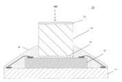
- FIG. 10 A schematic diagram showing an example of a radiation detection apparatus according to the present embodiment is shown in FIG.
- the radiation detection apparatus 10 has a configuration in which a photodetector 12, an adhesive layer 13, a scintillator 14 including a phosphor layer, and a dielectric multilayer reflective film 15 are installed on a support substrate 11. In one example, they have a stacked configuration.
- the support substrate 11 is not particularly limited as long as it can support the photodetector 12 and the scintillator 14 laminated thereon, and a glass substrate or a resin substrate is usually used. Further, by providing a conductive layer on the surface of the support substrate, the photodetector 12 and the surface of the support substrate 11 may be electrically connected using a bonding wire or the like.
- the size and thickness of the support substrate 11 are not particularly limited as long as the photodetector 12 and the scintillator 14 can be supported, but the size in the normal surface direction is equal to or greater than that of the photodetector 12.
- the photodetector 12 includes a photoelectric conversion unit facing the scintillator 14 and has a function of converting fluorescence emitted by the scintillator 14 into an electrical signal or the like.
- the photodetector 12 is not particularly limited, and a known photodetector can be used as appropriate.
- the photodetector 12 may include a protective resin 16 for protecting from an external impact.
- the protective resin is not particularly limited as long as the impact from the outside can be reduced, and the resin exemplified in the protective layer in the embodiment of the radiation image conversion screen may be used.
- the adhesive layer 13 only needs to be able to bond the scintillator 14 and the photodetector 12, and those exemplified in the adhesive layer in the embodiment of the radiation image conversion screen can be used.
- the scintillator 14 includes a phosphor that can absorb radiation and convert it into visible light. Usually, a sintered scintillator or a scintillator single crystal is used. When X-rays are used as radiation, a GOS sintered body or the like is used. When gamma rays are used as radiation, single crystals such as lutetium silicon oxide phosphors (LSO phosphors) such as LSO (Lu 3 SiO 5 : Ce), LYSO, LGSO, and LYGSO are preferably used.
- LSO phosphors lutetium silicon oxide phosphors
- LSO Lu 3 SiO 5 : Ce
- LYSO Li 3 SiO 5 : Ce
- LGSO LGSO
- LYGSO LYGSO
- the shape of the scintillator 14 is not particularly limited, but is generally a cube or a rectangular parallelepiped with all surfaces being rectangular.
- the scintillator 14 may be a single scintillator, and a plurality of scintillators may be arranged to form an array. In the case of forming an array, the number and size of scintillators are not particularly limited and can be appropriately set according to required functions.
- the dielectric multilayer reflective film 15 is a laminated film having an organic multilayer film structure using a polyester-based resin or urethane-based resin as a dielectric, and is a film that transmits radiation and has a high reflectance in the visible light range. .
- the description of the embodiment of the radiation image conversion screen is used for the description of the dielectric multilayer reflective film.
- a low refractive index layer or a low refractive index region is included on the surface of the dielectric multilayer reflective film opposite to the scintillator.
- the low refractive index means that the refractive index is lower than that of the dielectric multilayer reflective film, and a form that is a so-called space in which nothing exists above the dielectric multilayer reflective film 15 in the figure is preferable.
- the description of the low refractive index layer or the low refractive index region the description in the embodiment of the radiation image conversion screen is used.
- a dielectric multilayer reflective film is formed on one of a top surface and a bottom surface of a cubic or rectangular parallelepiped scintillator having a rectangular surface, and the scintillator of the derivative multilayer reflective film and A scintillator in which a low refractive index layer having a refractive index of 1.2 or less is adjacent to or in contact with the opposite surface, or a reflective layer is formed on at least one of the side surfaces of the scintillator. is there.
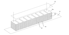
- FIG. 3 is a schematic perspective view showing an example of the scintillator according to the present embodiment.
- FIG. 3 shows a scintillator array 20 in which a plurality of rectangular parallelepiped scintillators 24 are arranged in a straight line.
- the plurality of scintillators 24 are arranged in a straight line in one row, but may be arranged in a straight line in two or more rows.
- the plurality of scintillators 24 are arranged on a straight line on the support substrate 21 via a photodetector (not shown) to form an array.
- a dielectric multilayer reflective film 25 is disposed on the plurality of scintillators 24. That is, the dielectric multilayer reflective film 25 is formed on the top surface of the scintillator 24.
- the top surface of the scintillator 24 and the dielectric multilayer reflective film 25 are in direct contact with each other, but another layer, between the top surface of the scintillator 24 and the dielectric multilayer reflective film 25, For example, an adhesive layer may be interposed.
- the surface opposite to the scintillator 24 of the dielectric multilayer reflective film 25 is a so-called space in which nothing exists. That is, the low refractive index region is in contact with the surface of the dielectric multilayer reflective film opposite to the scintillator.
- the scintillator 24 is a rectangular parallelepiped, but may be a cube.
- a reflective layer is formed on the entire side surface of the scintillator 24 indicated by hatching in FIG.
- the reflective layer may be formed on at least one of the side surfaces, and is preferably formed on the entire surface.
- the sensitivity of the scintillator can be improved by disposing the derivative multilayer reflective film on the X-ray incident surface (top surface) of the scintillator and disposing the reflective layer on the side surface.
- the reflective layer it is preferable to use a white resin, and specific examples thereof include a PET resin and a material in which TiO 2 , Al 2 O 3 or the like is dispersed.
- white means colorless and not transparent, and means a color that allows incident light to be irregularly reflected by a substance having no specific absorption wavelength in the visible light region.
- the reflectance of visible light in the white resin is preferably 80% or less.
- the thickness of the reflective layer is not particularly limited, and is usually 10 ⁇ m or more, preferably 50 ⁇ m or more, and usually 200 ⁇ m or less, preferably 100 ⁇ m or less.
- Example 1 20 parts by weight of a mixture of polyvinyl butyral resin, urethane resin fat and plasticizer was dissolved in 80 parts by weight of a mixed solvent of toluene, 2-butanol and xylene, and stirred sufficiently to prepare a binder. 13 parts by weight of this binder and 87 parts by weight of a Gd 2 O 2 S: Tb phosphor having an average particle size of 9 ⁇ m were mixed and sufficiently stirred, and further dispersed with a ball mill to obtain “phosphor composition 1”. Was prepared.
- the above-mentioned “phosphor composition 1” using a blade coater the phosphor coating weight after drying was 150 mg / cm 2 .
- the phosphor layer was formed on the organic multilayer reflective film and dried at 70 ° C. to 80 ° C. to form a laminate of the organic multilayer reflective film and the phosphor layer.
- a protective film made of a polyethylene terephthalate film having a thickness of 6 ⁇ m and having no light scattering property was applied to the surface of the formed phosphor layer.
- the surface of the optical film having the prism pattern and the surface of the organic multilayer reflective film not coated with the phosphor layer were bonded to each other.
- For bonding, only the outer peripheral portion of the optical film is bonded by laser welding so that the concave portion of the prism pattern of the optical film is not in contact with the surface of the organic multilayer reflective film on which the phosphor layer is not applied, and becomes a gap.
- the radiation image conversion screen 1 of Example 1 was obtained.
- Example 2 In Example 1, the radiation image conversion screen 2 of Example 2 was created in the same manner as in Example 1 except that the phosphor coating weight after drying was changed from 150 mg / cm 2 to 200 mg / cm 2 .
- Example 1 the substrate to which the phosphor is applied is a white polyethylene terephthalate film (Toray Lumirror E-60) which is a light reflective support having a thickness of 188 ⁇ m, and the light reflective support is optically coated.
- a radiation image conversion screen 3 of Comparative Example 1 was obtained in the same manner as in Example 1 except that the film was not bonded.
- Comparative Example 2 In Comparative Example 1, the radiation image conversion screen 4 of Comparative Example 2 was prepared in the same manner as in Comparative Example 1, except that the phosphor coating weight after drying was changed from 150 mg / cm 2 to 200 mg / cm 2 .
- Example 3 In the same manner as in Example 1, a protective film was attached to the laminate of the organic multilayer reflective film and the phosphor layer. Next, an optically transparent adhesive layer (Optically Clear Adhesive 8211 manufactured by 3M) has a refractive index of 1.47 in order to form a layer having a high refractive index on the opposite side of the phosphor layer of the organic multilayer reflective film. ) Were placed next to each other. Further, a white polyethylene terephthalate film (Toray Lumirror E-60) was bonded to the opposite side of the optical transparent adhesive layer of the organic multilayer reflective film to produce a radiation image conversion screen 5 of Comparative Example 3.
- an optically transparent adhesive layer Optically Clear Adhesive 8211 manufactured by 3M
- 3M has a refractive index of 1.47 in order to form a layer having a high refractive index on the opposite side of the phosphor layer of the organic multilayer reflective film.
- the radiation image conversion screens of the present invention (Examples 1 and 2) have both sharpness and sensitivity compared to the conventional radiation image conversion screens (Comparative Examples 1 and 2). ing.
- Comparative Example 3 the sensitivity is greatly reduced, and the effect of achieving both sharpness and sensitivity is not exhibited.
- Example B-1 To achieve the adhesive composition shown in Table 2, trade name Impranil DLH (manufactured by Sumika Bayer Urethane Co., Ltd.), which is a water-dispersible polyurethane resin, and trade name Nipol 1562 (ZEON, Japan), which is a water-dispersible acrylonitrile-butadiene copolymer was mixed at a ratio of 25/75 wt% to obtain a mixed solution.
- the ratio of the polyurethane resin (B) and the resin (C) different from the polyurethane resin (B) was 40:60 calculated from the concentration and mixing ratio of each water-dispersible resin.
- the above mixed solution was applied to an organic multilayer reflective film ESR (manufactured by 3M) having a thickness of 65 ⁇ m as a base material using an applicator and a thickness tape so that the dry thickness after drying was 10 ⁇ m. After application, the film was dried at 80 ° C. for 30 minutes to form an adhesive layer on the ESR.
- ESR organic multilayer reflective film
- the “phosphor composition 2” is applied to the ESR coated with the adhesive layer using a blade coater and a thickness tape so that the wet thickness (clearance between the ESR and the blade coater) is 600 ⁇ m.
- a phosphor layer was formed on the support and dried at a drying temperature of 70 ° C. to 80 ° C., thereby forming a phosphor layer and preparing Sample 1 for evaluating adhesiveness.
- the surface of the optical film having the prism pattern and the surface of the organic multilayer reflective film not coated with the phosphor layer were bonded to each other.
- the radiation image conversion screen 1 of Example B-1 was obtained.
- Laser welding was performed using a semiconductor laser welding machine manufactured by Enshu. The laser was irradiated from the optical film side, the laser peak wavelength was 940 nm, the spot diameter was 1.6 mm ⁇ , the irradiation output was 11 W, and the scanning speed was 1000 mm / min. Also, before laser welding, a commercially available black magic was applied to the laser irradiation spot (prism side) of the optical film so that the laser was absorbed during laser irradiation to facilitate welding.
- Example B-2 In Example B-1, the product name Implanil DLH (manufactured by Sumika Bayer Urethane Co., Ltd.), which is a water-dispersible polyurethane resin, and a water-dispersible styrene-butadiene copolymer so as to have the adhesive composition shown in Table 2 Except for mixing the product name Nipol LX430 (manufactured by Nippon Zeon Co., Ltd.) at a ratio of 75/25 wt%, the adhesive evaluation sample 2 and the radiation image conversion screen 2 of Example B-2 were prepared in the same manner as in Example 1. Created.
- Implanil DLH manufactured by Sumika Bayer Urethane Co., Ltd.
- Example B-3 In Example B-1, except that the mixed solution was applied so that the dry thickness after drying was 20 ⁇ m, Sample 3 for adhesion evaluation of Example B-3 and radiation were the same as Example B-1. An image conversion screen 3 was created.
- Example B-4 In Example B-1, the product name Implanil DLH (manufactured by Sumika Bayer Urethane Co., Ltd.), which is a water-dispersible polyurethane resin, and the product name Finetex, which is a water-dispersible polyester resin, so as to have the adhesive composition shown in Table 2
- Example B- was prepared in the same manner as Example B-1, except that ES675 (manufactured by DIC) was mixed at a ratio of 75/25 wt% and the mixed solution was applied so that the dry thickness after drying was 20 ⁇ m. Sample 4 for evaluating adhesiveness 4 and radiation image conversion screen 4 were prepared.
- Example B-5 In Example B-1, the product name Hyhydrol UH650 (manufactured by Sumika Bayer Urethane Co., Ltd.) which is a water-dispersible polyurethane resin and a product which is a water-dispersible styrene / butadiene copolymer so as to have the adhesive composition shown in Table 2
- Example 5-5 Adhesive evaluation sample 5 and radiation image conversion screen 5 in the same manner as Example B-1, except that the name Nipol LX430 (manufactured by Nippon Zeon Co., Ltd.) was mixed at a ratio of 75/25 wt%. It was created.
- Examples B-6 to B-8 In Examples B-1, except that the adhesive composition was changed as shown in Table 2, samples for adhesion evaluation of Examples B-6 to B-8 were prepared in the same manner as in Example B-1. .
- Reference examples B-1 and B-2 In Example B-1, the adhesion evaluation of Reference Examples B-1 and B-2 was performed in the same manner as in Example 2 except that the presence or absence of the adhesive layer and the wet thickness of the phosphor layer were changed as shown in Table 2. Sample and radiation image conversion screen were prepared.
- Example B1 Comparative Examples B1 and B2
- the base material was changed from an organic multilayer reflective film to a white polyethylene terephthalate film (Toray Lumirror E-60), which is a light reflective support having a thickness of 188 ⁇ m, and the adhesive composition and the adhesive layer dry were further changed. Except that the thickness and the wet thickness of the phosphor layer were changed as shown in Table 2, samples for evaluation of adhesiveness and radiation image conversion screens of Comparative Examples B1 and B2 were prepared in the same manner as in Example B1.
- a white polyethylene terephthalate film Toray Lumirror E-60
- the sensitivity and sharpness of the radiation image conversion screen were measured as follows.
- the radiation image conversion screens produced in Examples, Comparative Examples, and Reference Examples were attached to an X-ray camera (Remote RadEye2EV manufactured by TELEDYNERad-icon), and X-ray irradiation was performed on the X-ray camera to obtain an X-ray image.
- Sensitivity was obtained by irradiating an X-ray camera with no subject, and an X-ray image for sensitivity measurement having a uniform density throughout the image was obtained.
- the sensitivity was a relative value of the average output value of the X-ray image for sensitivity measurement for each radiation conversion screen.
- the sharpness was calculated by the so-called edge method MTF.
- a tungsten plate for MTF measurement having a thickness of 2 mm was installed as a subject on a part of the screen of an X-ray camera, and an edge image of the tungsten plate (an X-ray image having a density change depending on the presence or absence of the tungsten plate) was obtained.
- the MTF was calculated from the density change at the edge of the obtained X-ray image, and the MTF value at 2 Lp / mm when the MTF at the spatial frequency of 0 Lp / mm was normalized to 1 was defined as the sharpness.
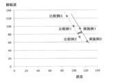
- Sensitivity and sharpness are in a trade-off relationship, and those near the line of Comparative Examples B-1 and B-2 in FIG. 4 indicate the sensitivity and sharpness, and Reference Examples B-1 to B- in FIG. Those near the two lines were marked with sensitivity and sharpness ⁇ , and those between the two lines were marked with ⁇ to ⁇ . As for the sensitivity sharpness, ⁇ and ⁇ to ⁇ are good results.
- the radiation image conversion screens (Examples B-1 to B-5) according to the present embodiment are different from the conventional radiation image conversion screens (Comparative Examples B-1 and B-2).
- the sensitivity and sharpness are improved without impairing the adhesion between the organic multilayer reflective film and the phosphor layer.
- Example C A TiO 2 dispersion (reflector paint BC620 manufactured by Saint-Gobain Co., Ltd.) with a thickness of 100 ⁇ m was applied as a white reflector on the side surface of the GOS sintered body cut to a size of 6 ⁇ 6 ⁇ 1.5 mm, and applied to the X-ray incident surface.
- the scintillator was created by changing the layer (film) provided as follows.
- Example C-1 65 ⁇ m thick organic multilayer reflective film ESR (manufactured by 3M)
- Example C-2 65 ⁇ m thick organic multilayer reflective film ESR (manufactured by 3M) provided with X-rays on the incident surface, and optical film BEF2-T-155n (manufactured by 3M) on the side opposite to the scintillator adjacent surface
- Comparative Example C-1 TiO 2 dispersion (reflector paint BC620 manufactured by Saint-Gobain Co., Ltd.) was applied in a thickness of 100 ⁇ m
- Comparative Example C-2 White polyethylene terephthalate film (Toray Lumirror E-60)
- the sensitivity of the prepared scintillator was measured by irradiating X-rays for 1 second and receiving scintillation light with a CMOS detector. The measurement results of scintillator sensitivity are shown in Table 3. The sensitivity is shown as a relative intensity with Comparative Example C-1 as 1.000.
- the scintillators of the present invention have improved sensitivity as compared with conventional scintillators (Comparative Examples C-1 and C-2).
Abstract
本発明は、トレードオフの関係にある感度及び鮮鋭度を両立した放射線像変換スクリーンを提供すること、また、該放射線像変換スクリーンを含む、高機能のフラットパネルディテクタを提供することを課題とする。本発明は、蛍光体層、有機多層反射膜を含む放射線像変換スクリーンであって、該有機多層反射膜の蛍光体層と反対側に、有機多層反射膜の屈折率未満の層を含むことを特徴とする放射線像変換スクリーンに存する。
Description
本発明は、放射線像変換スクリーン、フラットパネルディテクタ、放射線検出装置、及びシンチレータに存する。
従来、医療現場において、フィルムを用いたアナログ方式のX線画像が広く用いられてきた。しかし、近年、コンピューテッドラジオグラフィ(computed radiography:CR)やフラットパネル型の放射線ディテクタ(flat panel detector:FPD)等のデジタル方式が開発されている。
放射線を可視光に変換する間接方式のフラットパネルディテクタ(FPD:フラットパネルディテクタ)においては、放射線を可視光に変換するために、放射線像変換スクリーンが使用される。放射線像変換スクリーンは、タリウム賦活のヨウ化セシウム(CsI:Tl)やテルビウム賦活やプラセオジム賦活の酸硫化ガドリニウム(Gd2O2S:Tb、Gd2O2S:Pr)(GOS)等のX線蛍光体を含み、照射されたX線に応じて、該X線蛍光体が可視光を発光して、その発光をTFTやCCDなどを備えた光検出器で電気信号に変換することにより、X線の情報をデジタル画像情報に変換する。
FPDには、より照射X線に対する感度が高く、かつ高鮮鋭度のものが望まれている。感度を高めるためには放射線像変換スクリーンにおける蛍光体量を多くすることが有効であるが、蛍光体量を多くすると、放射線像変換スクリーンの厚みが増して蛍光体から発光した可視光がより広がりやすくなり鮮鋭度が低下する。この光の拡散の影響を抑え、鮮鋭度を保ったまま感度を向上させるために、例えば、特許文献1では、蛍光体の平均粒径や充填率、膜厚などを調整する方法が開示されている。
しかしながら、特許文献1の方法では、感度及び鮮鋭度が不十分である場合があった。
本発明は上記に鑑みてなされたものであり、トレードオフの関係にある感度及び鮮鋭度を両立した放射線像変換スクリーンを提供する。
また、本発明は、上記放射線像変換スクリーン及び光検出器を含む、高機能のフラットパネルディテクタを提供する。
更に本発明は、感度及び鮮鋭度を両立した放射線検出装置を提供する。
更に本発明は、感度及び鮮鋭度を両立したデバイスを提供できるシンチレータを提供する。
本発明は上記に鑑みてなされたものであり、トレードオフの関係にある感度及び鮮鋭度を両立した放射線像変換スクリーンを提供する。
また、本発明は、上記放射線像変換スクリーン及び光検出器を含む、高機能のフラットパネルディテクタを提供する。
更に本発明は、感度及び鮮鋭度を両立した放射線検出装置を提供する。
更に本発明は、感度及び鮮鋭度を両立したデバイスを提供できるシンチレータを提供する。
本発明者等は鋭意検討を行った結果、誘電体多層反射膜を用いた特定の層構成とすることで、上記課題を解決しうることを見出し、本発明に到達した。
即ち、本発明の要旨は、蛍光体層、及び該蛍光体層の一方の面側に形成された誘電体多層反射膜、を少なくとも備え、該誘電体多層反射膜の蛍光体層が形成された面と反対側の面に、屈折率が1.2以下の低屈折率層が隣接している、又は該誘電体多層反射膜の蛍光体層が形成された面と反対側の面が低屈折率領域と接している、放射線像変換スクリーンに存する。
即ち、本発明の要旨は、蛍光体層、及び該蛍光体層の一方の面側に形成された誘電体多層反射膜、を少なくとも備え、該誘電体多層反射膜の蛍光体層が形成された面と反対側の面に、屈折率が1.2以下の低屈折率層が隣接している、又は該誘電体多層反射膜の蛍光体層が形成された面と反対側の面が低屈折率領域と接している、放射線像変換スクリーンに存する。
また、本発明の別の要旨は、シンチレータ、該シンチレータの一方の側に設置された光検出器、及び該シンチレータの光検出器に設置された側と反対側に形成された誘導体多層反射膜、を有する放射線検出装置であって、
該誘電体多層反射膜のシンチレータと反対側の面に、屈折率が1.2以下の低屈折率層が隣接している、又は該誘電体多層反射膜のシンチレータと反対側の面が低屈折率領域と接している、放射線検出装置に存する。
該誘電体多層反射膜のシンチレータと反対側の面に、屈折率が1.2以下の低屈折率層が隣接している、又は該誘電体多層反射膜のシンチレータと反対側の面が低屈折率領域と接している、放射線検出装置に存する。
また、本発明の別の要旨は、矩形面からなる立方体又は直方体状のシンチレータの頂面及び底面のうち一方の面に誘電体多層反射膜が形成され、該誘導体多層反射膜の該シンチレータと反対側の面に、屈折率が1.2以下の低屈折率層が隣接しており又は低屈折率領域が接しており、該シンチレータの側面のうち少なくとも一面に反射層が形成された、シンチレータに存する。
本発明により、トレードオフの関係にある感度及び鮮鋭度を両立した放射線像変換スクリーンを提供することが可能となる。
また、本発明により、上記放射線像変換スクリーンを含む、高機能のフラットパネルディテクタを提供することが可能となる。更に、高い感度を有する放射線検出装置、及びシンチレータを提供することが可能となる。
また、本発明により、上記放射線像変換スクリーンを含む、高機能のフラットパネルディテクタを提供することが可能となる。更に、高い感度を有する放射線検出装置、及びシンチレータを提供することが可能となる。
以下、本発明について実施形態や例示物を示して説明するが、本発明は以下の実施形態や例示物等に限定されるものではなく、本発明の要旨を逸脱しない範囲において任意に変形して実施することができる。
尚、本明細書において「~」を用いて表される数値範囲は、「~」の前後に記載される数値を下限値及び上限値として含む範囲を意味する。
以下、図1を用いて本発明の実施形態に係る放射線像変換スクリーン、およびそれを用いたフラットパネルディテクタ(以下、「FPD」と称する場合がある)の好ましい構成について説明するが、本発明はこれらに限定されない。
尚、本明細書において「~」を用いて表される数値範囲は、「~」の前後に記載される数値を下限値及び上限値として含む範囲を意味する。
以下、図1を用いて本発明の実施形態に係る放射線像変換スクリーン、およびそれを用いたフラットパネルディテクタ(以下、「FPD」と称する場合がある)の好ましい構成について説明するが、本発明はこれらに限定されない。
フラットパネルディテクタ1は、放射線像変換スクリーン2、光検出器3、および電源部(図示しない)からなる。放射線像変換スクリーン2は、X線等の入射された放射線のエネルギーを吸収して、波長が300nmから800nmの範囲の電磁波、すなわち、可視光線を中心に紫外光から赤外光にわたる範囲の電磁波(光)を発光する。
放射線像変換スクリーン2は、プリズムシート4、プリズムシート4と誘電体多層膜との間に存在する屈折率が1.2以下の低屈折率層である空気層5、誘電体多層反射層6、接着層7、蛍光体層8、及び保護層9を含む。
放射線像変換スクリーン2は、その出光面と光検出器3とを、保護層9を介して、接着又は密着させることでフラットパネルディテクタ1となる。放射線像変換スクリーン2で発光した光が、光検出器3に到達して光電変換を行い、出力する。以下、各構成部材について、説明する。
放射線像変換スクリーン2は、その出光面と光検出器3とを、保護層9を介して、接着又は密着させることでフラットパネルディテクタ1となる。放射線像変換スクリーン2で発光した光が、光検出器3に到達して光電変換を行い、出力する。以下、各構成部材について、説明する。
[蛍光体層]
本発明に用いる蛍光体層は、蛍光体を含む層である。
本実施形態において蛍光体は、X線等の入射された放射線のエネルギーを吸収して、波長が300nmから800nmの電磁波、すなわち、可視光線を中心に紫外光から赤外光にわたる電磁波(光)を発光する物質をいう。
蛍光体層に含まれる蛍光体の種類は、本発明の効果を損なわない限り特に制限はないが、X線から可視光への変換効率が高く、また発光された可視光を吸収しにくいものが好ましい。
本発明に用いる蛍光体層は、蛍光体を含む層である。
本実施形態において蛍光体は、X線等の入射された放射線のエネルギーを吸収して、波長が300nmから800nmの電磁波、すなわち、可視光線を中心に紫外光から赤外光にわたる電磁波(光)を発光する物質をいう。
蛍光体層に含まれる蛍光体の種類は、本発明の効果を損なわない限り特に制限はないが、X線から可視光への変換効率が高く、また発光された可視光を吸収しにくいものが好ましい。
例えば、特開2000-162394号公報や特開2003-82347号公報に記載の如く、酸硫化ガドリニウム蛍光体(Gd2O2S)に、テルビウム(Tb)、ジルプロシウム(Dy)、セシウム(Ce)などの賦活物質を含有する蛍光体(以下、これらをGOS蛍光体とも称する)ものを用いることができる。
また、特開2011-7522号公報に記載の如く、CsIや、CsIとヨウ化ナトリウム(NaI)を任意のモル比で混合したものや、特開2001-59899号公報に記載の如く、CsIにンジウム(In)、タリウム(Tl)、リチウム(Li)、カリウム(K)、ルビジウム(Rb)、ナトリウム(Na)などの賦活物質を含有する蛍光体(以下、これらをCsI蛍光体とも称する)を用いてもよい。
蛍光体層は、特に、GOS蛍光体を含むことが、好ましい。
蛍光体層に含まれる蛍光体は、1種を単独で用いてもよく、異なる2種以上を併用してもよい。
また、特開2011-7522号公報に記載の如く、CsIや、CsIとヨウ化ナトリウム(NaI)を任意のモル比で混合したものや、特開2001-59899号公報に記載の如く、CsIにンジウム(In)、タリウム(Tl)、リチウム(Li)、カリウム(K)、ルビジウム(Rb)、ナトリウム(Na)などの賦活物質を含有する蛍光体(以下、これらをCsI蛍光体とも称する)を用いてもよい。
蛍光体層は、特に、GOS蛍光体を含むことが、好ましい。
蛍光体層に含まれる蛍光体は、1種を単独で用いてもよく、異なる2種以上を併用してもよい。
また、蛍光体層に含まれる蛍光体の平均粒径は、通常30μm以下、好ましくは15μm以下、また通常0.05μm以上、好ましくは0.1μm以上である。
上記範囲内であると、光を散乱する効果が大きく、得られる放射線像変換スクリーンの感度が良好である点で好ましい。
上記範囲内であると、光を散乱する効果が大きく、得られる放射線像変換スクリーンの感度が良好である点で好ましい。
(蛍光体の充填率)
蛍光体層における蛍光体の充填率は、通常40%以上、好ましくは50%以上、更に好ましくは60%以上、また通常100%以下である。
上記範囲内であると、入射するX線を効率的に可視光に変換できる点で好ましい。
尚、充填率の測定方法は、下記の通り行う。
塗布前の基板の重さ(W0)と、蛍光体層を形成した後の重さ(W1)を測定する。形成された蛍光体を含む層の膜厚及び面積と、測定した膜の重さ(W1-W0)から、単位体積当りの重さを算出する。
一方、蛍光体と媒質の重さの比より、層中に含有される蛍光体の単位体積当りの重さを算出する。算出された蛍光体の単位体積当りの含有量と、蛍光体の比重から、蛍光体の充填率(体積%)を算出することが可能となる。
(蛍光体層の蛍光体積層量)
蛍光体層の蛍光体積層量は特に限定されず、放射線像変換スクリーンの大きさや、要求される感度により適宜設定できる。蛍光体粒子が積層されることで蛍光体層を形成することが好ましく、通常20mg/cm2以上、好ましくは100mg/cm2以上であり、また通常1000mg/cm2以下、好ましくは500mg/cm2以下である。本実施形態に係る放射線像変換スクリーンは、高エネルギーの放射線での使用に適しており、その場合、蛍光体積層量は通常150mg/cm2以上、300mg/cm2以下であることが好ましい。
蛍光体層の蛍光体積層量は特に限定されず、放射線像変換スクリーンの大きさや、要求される感度により適宜設定できる。蛍光体粒子が積層されることで蛍光体層を形成することが好ましく、通常20mg/cm2以上、好ましくは100mg/cm2以上であり、また通常1000mg/cm2以下、好ましくは500mg/cm2以下である。本実施形態に係る放射線像変換スクリーンは、高エネルギーの放射線での使用に適しており、その場合、蛍光体積層量は通常150mg/cm2以上、300mg/cm2以下であることが好ましい。
[蛍光体層の形成方法]
蛍光体層の形成方法としては特段の限定は無く、例えば真空蒸着法により層を形成する方法や湿式成膜法により層を形成する方法が挙げられる。
以下、蛍光体含有組成物を用いる湿式成膜法により層を形成する方法について詳説する。
蛍光体層の形成方法としては特段の限定は無く、例えば真空蒸着法により層を形成する方法や湿式成膜法により層を形成する方法が挙げられる。
以下、蛍光体含有組成物を用いる湿式成膜法により層を形成する方法について詳説する。
湿式成膜法で蛍光体層を形成する場合、その工程には通常、蛍光体含有組成物調製工程、塗布工程、及び乾燥工程、を含む。尚、乾燥工程後に、後処理工程(洗浄、乾燥などを行う工程)を任意に含んでいてもよい。
(蛍光体含有組成物調製工程)
蛍光体含有組成物調製工程では、蛍光体含有組成物を調製する。蛍光体含有組成物は、形状は粉末であってもスラリー状のものであってもよい。
蛍光体含有組成物は、前記蛍光体を含み、必要に応じてその他の媒質、例えば、バインダー樹脂、分散剤、可塑剤、光重合性開始剤/熱重合開始剤等を含有させてもよい。また、組成物の粘度を調整する為に、有機溶剤などを含んでいてもよい。
蛍光体含有組成物調製工程では、蛍光体含有組成物を調製する。蛍光体含有組成物は、形状は粉末であってもスラリー状のものであってもよい。
蛍光体含有組成物は、前記蛍光体を含み、必要に応じてその他の媒質、例えば、バインダー樹脂、分散剤、可塑剤、光重合性開始剤/熱重合開始剤等を含有させてもよい。また、組成物の粘度を調整する為に、有機溶剤などを含んでいてもよい。
蛍光体含有組成物に含有されてもよいバインダー樹脂としては、本発明の効果を損なわない限り特に制限はないが、例えば、硝化綿、酢酸セルロース、エチルセルロース、ポリビニルブチラール、線状ポリエステル、ポリ酢酸ビニル、塩化ビニリデン・塩化ビニルコポリマー、塩化ビニル・酢酸ビニルコポリマー、ポリアルキル-(メタ)アクリレート、ポリカーボネート、ポリウレタン、セルロースアセテートブチレート、ポリビニルアルコール、ゼラチン、デキストリン等のポリサッカライド、アラビアゴムなどが挙げられる。
蛍光体含有組成物にバインダー樹脂を含有させる場合には、蛍光体含有組成物全量に対しバインダー樹脂が通常0.1重量%以上、好ましくは2.0重量%以上であり、また通常20重量%以下、好ましくは10重量%以下である。
蛍光体含有組成物にバインダー樹脂を含有させる場合には、蛍光体含有組成物全量に対しバインダー樹脂が通常0.1重量%以上、好ましくは2.0重量%以上であり、また通常20重量%以下、好ましくは10重量%以下である。
また、分散剤としては、本発明の効果を損なわない限り特に制限はないが、例えば、フタル酸、ステアリン酸などが挙げられる。
更に、可塑剤としては、リン酸トリフェニル、フタル酸ジブチルなどが挙げられる。
これら材料は、1種を単独で用いてもよく、異なる2種以上を併用してもよい。
更に、可塑剤としては、リン酸トリフェニル、フタル酸ジブチルなどが挙げられる。
これら材料は、1種を単独で用いてもよく、異なる2種以上を併用してもよい。
蛍光体含有組成物に含有されていてもよい有機溶剤としては、上記蛍光体及び媒質を溶解又は分散できるものであれば特に制限はないが、例えば、エタノール、メチルエチルエーテル、酢酸ブチル、酢酸エチル、エチルエーテル、キシレンなどが挙げられる。有機溶剤は、1種を単独で用いてもよく、異なる2種以上を併用してもよい。
尚、蛍光体と媒質との屈折率差が大きいほど、蛍光体粒子における光散乱効果が大きく、蛍光体から発光した光を凹部に集光しやすい点で、媒質の屈折率は、1.3以下が好ましく、1.1以下が更に好ましい。
蛍光体を含む上記原料を、適宜混合・撹拌することで、蛍光体含有組成物を調製できる。
蛍光体を含む上記原料を、適宜混合・撹拌することで、蛍光体含有組成物を調製できる。
(塗布工程、乾燥工程)
塗布工程では、調製した蛍光体含有組成物を支持体上に塗布し、塗膜を形成する。
塗布による塗膜の形成方法としては、本発明の効果を損なわない限り特に制限はなく公知の技術が適用可能であるが、例えば、ダイコート法、スクリーン印刷法、インクジェット法、スピンコーター法などが挙げられる。
形成された塗膜は、ホットプレートや温風乾燥機等を使って乾燥または熱硬化させ、或いは紫外線照射装置などを用いて光硬化させることで、蛍光体層を得る。
蛍光体層は、異なる2種以上の膜を積層することで、多層を形成していてもよい。多層とする場合、例えば、蛍光体の平均粒径や粒度分布、又は含有される媒質などが異なる層を適宜積層できる。
塗布工程では、調製した蛍光体含有組成物を支持体上に塗布し、塗膜を形成する。
塗布による塗膜の形成方法としては、本発明の効果を損なわない限り特に制限はなく公知の技術が適用可能であるが、例えば、ダイコート法、スクリーン印刷法、インクジェット法、スピンコーター法などが挙げられる。
形成された塗膜は、ホットプレートや温風乾燥機等を使って乾燥または熱硬化させ、或いは紫外線照射装置などを用いて光硬化させることで、蛍光体層を得る。
蛍光体層は、異なる2種以上の膜を積層することで、多層を形成していてもよい。多層とする場合、例えば、蛍光体の平均粒径や粒度分布、又は含有される媒質などが異なる層を適宜積層できる。
[誘電体多層反射膜]
誘電体多層反射膜とは、誘電体であるポリエステル系樹脂、ウレタン樹脂等を用いた有機多層膜構造を有した積層フィルムである。放射線を透過し、且つ可視光範囲における反射率が高い膜であることが好ましい。
反射率が高い膜とは、可視光範囲における反射率の平均値、特には波長350nm以上750nm以下の波長領域における反射率の平均値が、90%以上であり、好ましくは95%以上である膜を意味する。また、光学用途であることから、面の均一性が高いものが好ましい。また、多層とは2層以上であればよく、通常10層以下であり、5層以下であってもよい。
誘電体多層反射膜とは、誘電体であるポリエステル系樹脂、ウレタン樹脂等を用いた有機多層膜構造を有した積層フィルムである。放射線を透過し、且つ可視光範囲における反射率が高い膜であることが好ましい。
反射率が高い膜とは、可視光範囲における反射率の平均値、特には波長350nm以上750nm以下の波長領域における反射率の平均値が、90%以上であり、好ましくは95%以上である膜を意味する。また、光学用途であることから、面の均一性が高いものが好ましい。また、多層とは2層以上であればよく、通常10層以下であり、5層以下であってもよい。
放射線像変換スクリーンが可視光に対して高い反射率を有する膜を含むことで、蛍光体層から発せられた光のうち、光検出器と反対方向に向かう光を反射させて光検出器に向かう光とすることで、光検出器で検出される光量が増える。その為、放射線像変換スクリーンの感度が向上する。
誘電体多層反射膜は、放射線を透過し、かつ高い可視光反射率を有する積層フィルムであれば特に制限はないが、例えば、3M社製ESR(Enhanced Specular Reflector) などが好適に挙げられる。
誘電体多層反射膜は、放射線を透過し、かつ高い可視光反射率を有する積層フィルムであれば特に制限はないが、例えば、3M社製ESR(Enhanced Specular Reflector) などが好適に挙げられる。
誘電体多層反射膜の可視光における反射率の平均値は、より多くの光を出力基板に向かわせることで放射線像変換スクリーンの感度を向上させる点で、98%以上であることが特に好ましい。なお、誘電体多層反射膜の反射率は、誘電体多層反射膜を構成するそれぞれの有機膜の表面を適宜粗らすことや、積層する有機膜の屈折率を適宜調整することで調整することができる。また、蛍光体層から発せられる蛍光波長に応じて、層構成を調整し、最適化することができる。そのため、誘電体多層反射膜を構成する膜は、有機膜、無機膜のどちらであってもよく、フレキシビリティーの観点から有機膜が好ましいものの特に限定されるものではない。
(屈折率)
誘電体多層反射膜の屈折率は、通常1.35以上、好ましくは1.45以上である。上限は特に限定されないが、通常2.0以下である。
上記範囲内であると、本発明の効果が良好に得られる点で好ましい。
(誘電体多層反射膜の厚み)
誘電体多層反射膜の厚みは特段限定されず、放射線像変換スクリーンの大きさに応じて適宜設定できる。通常100nm以上、好ましくは20μm以上であり、また通常1000μm以下、好ましくは100μm以下である。
誘電体多層反射膜の屈折率は、通常1.35以上、好ましくは1.45以上である。上限は特に限定されないが、通常2.0以下である。
上記範囲内であると、本発明の効果が良好に得られる点で好ましい。
(誘電体多層反射膜の厚み)
誘電体多層反射膜の厚みは特段限定されず、放射線像変換スクリーンの大きさに応じて適宜設定できる。通常100nm以上、好ましくは20μm以上であり、また通常1000μm以下、好ましくは100μm以下である。
[低屈折率層、乃至は低屈折率領域]
放射線像変換スクリーンは、誘電体多層反射膜の蛍光体層と反対側に、低屈折率層乃至は低屈折率領域を含む。ここで低屈折率とは、誘電体多層反射膜よりも低屈折率であることを意味する。
このように、誘電体多層反射膜の蛍光体層と反対側の面が、低屈折率層または低屈折領域であることで、蛍光体層から発せられた光のうち、光検出器と反対方向に向かう光であって誘電体多層反射膜を透過してしまう光を、誘電体多層反射膜と低屈折層との界面で反射させることができる。反射された該光は、再度光検出器方向に向かうため、誘電体多層反射膜の反射効率を更に高めることが可能となり、放射線像変換スクリーンの感度をより高めることができる。結果、放射線像変換スクリーンにおける感度及び鮮鋭度のトレードオフ曲線を、望ましい方向にシフトさせることができる。
低屈折率層乃至は低屈折率領域は、誘電体多層反射膜よりも低屈折率であればよく、例えば、低屈折率である樹脂層であってよく、単なる空隙(空間)である空気層であってよく、真空層であってもよい。定量的には、通常屈折率が1.3以下であり、1.2以下であることが好ましく、1.1以下であることが更に好ましい。導電体多層反射膜との屈折率差が大きく、本発明の効果が良好に得られる点で、低屈折率層乃至は低屈折率領域が空気層又は空隙(空間)であることが好ましい。
低屈折率層乃至は低屈折率領域を空気層とする場合、誘電体多層反射膜の蛍光体層と反対側に、表面に凹凸を有する膜、例えば、図1のプリズムシート4のようなシート(層)を設置することで、表面に存在するプリズムパターンの凹部分が誘電体多層反射膜と接触せずに空隙となるようにして、空気層を形成してもよい。
尚、プリズムシートは、誘電体多層反射膜の強度が弱い場合にその支持のために設置されるものである。その為、誘電体多層反射膜が、単独で十分な支持強度を有する場合は、プリズムシートを設置しなくてもよい。この場合、誘電体多層反射膜の蛍光体層と反対側には、いずれの層も存在しない空間状態である。このような状態は、誘電体多層反射膜の蛍光体層が形成された面と反対側の面が低屈折率領域と接している状況である。
[プリズムシート]
プリズムシートとは、プラスチックフィルム(樹脂フィルム)などのプラスチック製の支持体の表面に、アクリル樹脂等で微細なプリズムパターンを均一に精密形成した光学フィルムである。なおプリズムパターンは、誘電体多層反射膜との間に空気の層が存在し得る状態であればよいため、プリズムパターンがアトランダムであってもよい。
用いるプリズムシートは、誘電体多層反射膜との間に空気の層が存在し得る限り特に制限はないが、例えば、3M社BEF2-T-155nなどが挙げられる。
中でも、本発明の効果が良好に得られる点で、プリズムピッチはFPDの画素ピッチより小さいことが好ましく、通常100μm以下、好ましくは50μm以下である。
[光検出器]
光検出器は、蛍光体層に対向して光電変換部を備え、蛍光体層で発せられた蛍光を、電気信号等に変換する機能を有する。このような機能を有する限り光検出器は特段限定されず、既知の光検出器を適宜用いることができる。
光検出器は、蛍光体層に対向して光電変換部を備え、蛍光体層で発せられた蛍光を、電気信号等に変換する機能を有する。このような機能を有する限り光検出器は特段限定されず、既知の光検出器を適宜用いることができる。
[接着層]
本実施形態に係る放射線像変換スクリーンは、誘電体多層反射膜と蛍光体層との間に接着層を有してもよい。接着層を含むことで、放射線像変換スクリーンにおける感度及び鮮鋭度のトレードオフ曲線を、望ましい方向にシフトさせることができる。
接着層は、本発明の効果を損なわずに有機多層反射膜と蛍光体層とが接着されるようであればその材料は特に限定されず、例えば、ポリウレタン樹脂、スチレン・ブタジエン共重合体、アクリロニトリル・ブタジエン共重合体、ポリエステル樹脂、クロロプレン樹脂、シリコーン樹脂、エポキシ樹脂等が挙げられ、中でも接着性及び光学特性(感度と鮮鋭度)の観点から、ポリウレタン樹脂、スチレン・ブタジエン共重合体、アクリロニトリル・ブタジエン共重合体、ポリエステル樹脂が好ましく、特にポリウレタン樹脂が好ましい。接着剤として用いる樹脂は、その樹脂単独でもよいし、本発明を損なわない範囲において、他の成分との共重合体でもよい。また、本発明を損なわない範囲において、例えばカルボキシル基、スルホン酸基、アミノ基等で変性されてもよく、これらの官能基の一部の水素がアルカリ金属やアルカリ土類金属に置き換わってもよい。
本実施形態で用いる接着剤は、水分散系、溶液系、反応系、ホットメルト系等、いずれの分類であってもよいが、水分散系、溶液系が好ましく、特に水分散系が好ましい。
また接着層は、1種または2種以上の樹脂を含むことが好ましく、ポリウレタン樹脂、スチレン・ブタジエン共重合体、アクリロニトリル・ブタジエン共重合体、ポリエステル樹脂からなる群から選ばれる1種または2種以上の樹脂を含むことがより好ましい。接着層の層構成は特に限定されず、1層のみで形成されていてもよく2層以上の多層であってもよい。例えば、有機多層反射膜の上面にポリウレタン樹脂層と、ポリウレタン樹脂とは異なる樹脂層とで構成されてもよいし、ポリウレタン樹脂と、ポリウレタン樹脂とは異なる樹脂とを予め混合した後に混合接着層として構成されてもよい。
また接着層は、1種または2種以上の樹脂を含むことが好ましく、ポリウレタン樹脂、スチレン・ブタジエン共重合体、アクリロニトリル・ブタジエン共重合体、ポリエステル樹脂からなる群から選ばれる1種または2種以上の樹脂を含むことがより好ましい。接着層の層構成は特に限定されず、1層のみで形成されていてもよく2層以上の多層であってもよい。例えば、有機多層反射膜の上面にポリウレタン樹脂層と、ポリウレタン樹脂とは異なる樹脂層とで構成されてもよいし、ポリウレタン樹脂と、ポリウレタン樹脂とは異なる樹脂とを予め混合した後に混合接着層として構成されてもよい。
接着層の塗布方法は、本発明の効果を損なわない限り特に制限はなく公知の技術が適用可能であるが、例えば、ダイコート法、スクリーン印刷法、インクジェット法、スピンコーター法などが挙げられる。また、接着剤を塗布した後に、乾燥工程、後処理工程(洗浄、乾燥)等を任意に含んでいてもよい。
接着層の厚みは、本発明の効果を損なわない限り特に制限はないが、通常0.1~100μm、好ましくは0.5~30μm、さらに好ましくは1~20μmである。
上記範囲内であると有機多層反射膜と蛍光体層との密着性が良好であり、且つ感度および鮮鋭度などの光学特性が良好である点で好ましい。
接着層の厚みは、本発明の効果を損なわない限り特に制限はないが、通常0.1~100μm、好ましくは0.5~30μm、さらに好ましくは1~20μmである。
上記範囲内であると有機多層反射膜と蛍光体層との密着性が良好であり、且つ感度および鮮鋭度などの光学特性が良好である点で好ましい。
[保護膜]
上記蛍光層を形成後、更に蛍光体層の上に保護層を形成していてもよい。
保護層を形成する材料は、本発明の効果を損なわない限り特に制限はないが、例えば、ウレタン(メタ)アクリレート、単官能(メタ)アクリレート、多官能(メタ)アクリレートを含有する放射線硬化性組成物の硬化物等や、粘着層を有するPET等のフィルムがある。前述の放射線硬化性組成物中には、必要に応じて適宜上記以外の材料が含有されていてもよい。
上記蛍光層を形成後、更に蛍光体層の上に保護層を形成していてもよい。
保護層を形成する材料は、本発明の効果を損なわない限り特に制限はないが、例えば、ウレタン(メタ)アクリレート、単官能(メタ)アクリレート、多官能(メタ)アクリレートを含有する放射線硬化性組成物の硬化物等や、粘着層を有するPET等のフィルムがある。前述の放射線硬化性組成物中には、必要に応じて適宜上記以外の材料が含有されていてもよい。
本発明の別の実施形態は、シンチレータ、該シンチレータの一方の側に設置された光検出器、及び該シンチレータの光検出器に設置された側と反対側に形成された誘導体多層反射膜、を有する放射線検出装置である。本実施形態に係る放射線光検出器は、該誘電体多層反射膜のシンチレータと反対側の面に、屈折率が1.2以下の低屈折率層が隣接している、又は該誘電体多層反射膜のシンチレータと反対側の面が低屈折率領域と接している、放射線検出装置である。
このように、誘電体多層反射膜のシンチレータと反対側の面が、低屈折率層または低屈折領域であることで、蛍光体層から発せられた光のうち、光検出器と反対方向に向かう光であって誘電体多層反射膜を透過してしまう光を、誘電体多層反射膜と低屈折層との界面で反射させることができる。反射された該光は、再度光検出器に向かうため、誘電体多層反射膜の反射効率を更に高めることが可能となり、放射線検出装置の感度をより高めることができる。結果、放射線検出装置における感度及び鮮鋭度のトレードオフ曲線を、望ましい方向にシフトさせることができる。
本実施形態に係る放射線検出装置の一例を示す模式図を図2に示す。
放射線検出装置10は、支持基板11上に光検出器12、接着層13、蛍光体層を含むシンチレータ14及び誘電体多層反射膜15が設置された構成を有する。一例では、これらは積層された構成を有する。
放射線検出装置10は、支持基板11上に光検出器12、接着層13、蛍光体層を含むシンチレータ14及び誘電体多層反射膜15が設置された構成を有する。一例では、これらは積層された構成を有する。
支持基板11は、その上に積層される光検出器12やシンチレータ14を支持できれば特段限定されず、通常ガラス基板や樹脂基板などが用いられる。また、支持基板表面に導電性を有する層を備えることで、光検出器12と支持基板11の表面とをボンディングワイヤ等を用いて電気的に接続してもよい。支持基板11の大きさ、厚さは、光検出器12とシンチレータ14を支持できれば特段制限はないが、通常面方向の大きさが、光検出器12と同等またはそれ以上である。
光検出器12は、シンチレータ14に対向して光電変換部を備え、シンチレータ14で発せられた蛍光を電気信号等に変換する機能を有する。光検出器12は特段限定されず、既知の光検出器を適宜用いることができる。また、一形態では、光検出器12は外部からの衝撃から保護するための保護樹脂16を備えていてもよい。保護樹脂は、外部からの衝撃を緩和できれば特に限定されず、上記放射線像変換スクリーンの実施形態における保護層で例示された樹脂を使用してもよい。
接着層13は、シンチレータ14と光検出器12とを接着することができればよく、上記放射線像変換スクリーンの実施形態における接着層で例示されたものを用いることができる。
シンチレータ14は、放射線を吸収し可視光に変換し得る蛍光体を含み、通常、焼結シンチレータ又はシンチレータ単結晶が使用される。放射線としてX線を用いる場合は、GOSの焼結体等が用いられる。放射線としてγ線を用いる場合はLSO(Lu3SiO5:Ce)、LYSO、LGSO、LYGSO等のルテチウムケイ素酸化物蛍光体(LSO系蛍光体)等の単結晶が好適に用いられる。シンチレータ14の形状は特段限定されないが、全ての面が矩形である立方体や直方体であることが一般的である。シンチレータ14は、1つのシンチレータであってよく、複数のシンチレータが配置されてアレイを形成していてもよい。アレイを形成する場合、シンチレータの数や大きさに特段の制限はなく、要求される機能等に応じて適宜設定できる。
誘電体多層反射膜15は誘電体であるポリエステル系樹脂又はウレタン系樹脂等を用いた有機多層膜構造を有した積層フィルムで、放射線を透過し、かつ可視光範囲における反射率が高い膜である。誘電体多層反射膜の説明は、上記放射線像変換スクリーンの実施形態における説明が援用される。
本実施形態では、誘電体多層反射膜のシンチレータと反対側の面に、低屈折率層乃至は低屈折率領域を含む。ここで低屈折率とは、誘電体多層反射膜よりも低屈折率であることを意味し、図中誘電体多層反射膜15の上方に何も存在しない、いわゆる空間である形態が好ましい。低屈折率層乃至は低屈折率領域の説明は、上記放射線像変換スクリーンの実施形態における説明が援用される。
本実施形態では、誘電体多層反射膜のシンチレータと反対側の面に、低屈折率層乃至は低屈折率領域を含む。ここで低屈折率とは、誘電体多層反射膜よりも低屈折率であることを意味し、図中誘電体多層反射膜15の上方に何も存在しない、いわゆる空間である形態が好ましい。低屈折率層乃至は低屈折率領域の説明は、上記放射線像変換スクリーンの実施形態における説明が援用される。
また、本発明の別の実施形態は、矩形面からなる立方体又は直方体状のシンチレータの頂面及び底面のうち一方の面に誘電体多層反射膜が形成され、該誘導体多層反射膜の該シンチレータと反対側の面に、屈折率が1.2以下の低屈折率層が隣接しており又は低屈折率領域が接しており、該シンチレータの側面のうち少なくとも一面に反射層が形成されたシンチレータである。
本実施形態に係るシンチレータの一例を示す斜視模式図を図3に示す。
本実施形態に係るシンチレータの一例を示す斜視模式図を図3に示す。
図3は、矩形面からなる直方体のシンチレータ24が複数直線状に配置されたシンチレータアレイ20を示す。図3では、複数のシンチレータ24は一列で直線に配置されるが、2列以上で直線状に配置されてもよい。複数のシンチレータ24は、支持基板21上に光検出器(図示せず)を介して直線上に配置されて、アレイを形成している。複数のシンチレータ24の上部には、誘電体多層反射膜25が配置される。すなわち、シンチレータ24の頂面に、誘電体多層反射膜25が形成される。なお、図3では、シンチレータ24の頂面と誘電体多層反射膜25とが直接接する構成となっているが、シンチレータ24の頂面と誘電体多層反射膜25との間に、他の層、例えば接着層などを介してもよい。
誘電体多層反射膜25のシンチレータ24と反対の面は何も存在しない、いわゆる空間となっている。すなわち、誘導体多層反射膜のシンチレータと反対側の面に低屈折率領域が接している。
本実施形態ではシンチレータ24は直方体であるが、立方体であってもよい。本実施形態では、図3中ハッチングで示されるシンチレータ24の側面には、全面に反射層が形成される。反射層は、側面のうち少なくとも1面に形成されればよく、全面に形成されていることが好ましい。シンチレータ24の側面に反射層が形成されることで、シンチレータの感度が向上する。すなわち本実施形態では、シンチレータにおけるX線入射面(頂面)には誘導体多層反射膜が配置され、側面には反射層が配置されることで、シンチレータの感度を向上させることができる。
反射層としては、白色樹脂を用いることが好ましく、具体例としてはPET樹脂、及びこれにTiO2やAl2O3などを分散させたものがあげられる。ここで「白色」とは、無色であり透明ではないことを意味し、可視光領域に特異な吸収波長を持たない物質により入射光を乱反射させる事ができる色をいう。白色樹脂における可視光の反射率は、80%以下であることが好ましい。
反射層の厚みは特段限定されず、通常10μm以上、好ましくは50μm以上、また通常200μm以下、好ましくは100μm以下である。
以下、本発明を実施例によりさらに具体的に説明するが、本発明はその要旨を逸脱しない限り、以下の実施例に限定されるものではない。
[放射線像変換スクリーンの作製]
(実施例1)
ポリビニルブチラール樹脂、ウレタン樹脂脂及び可塑剤の混合物20重量部を、トルエン、2-ブタノール及び、キシレンの混合溶剤80重量部に溶解し、十分に攪拌して結合剤を作成した。 この結合剤13重量部と平均粒子径9μmのGd2O2S:Tb蛍光体87重量部とを混合して充分に撹拌し、さらにこれをボールミルで分散処理して「蛍光体組成物1」を調製した。
(実施例1)
ポリビニルブチラール樹脂、ウレタン樹脂脂及び可塑剤の混合物20重量部を、トルエン、2-ブタノール及び、キシレンの混合溶剤80重量部に溶解し、十分に攪拌して結合剤を作成した。 この結合剤13重量部と平均粒子径9μmのGd2O2S:Tb蛍光体87重量部とを混合して充分に撹拌し、さらにこれをボールミルで分散処理して「蛍光体組成物1」を調製した。
次いで、厚さ65μmの有機多層反射膜ESR(3M社製)を基材として、前記「蛍光体組成物1」をブレードコータを使用して、乾燥後の蛍光体塗布重量が150mg/cm2となるように塗布して蛍光体層を有機多層反射膜上に形成し、70℃から80℃で乾燥させることによって、有機多層反射膜と蛍光体層の積層体を形成した。形成した蛍光体層の表面に、感熱性接着剤(日本合成化学製 ポリエスター TP220)を塗布した、厚さ6μmの光散乱性のないポリエチレンテレフタレートフィルムからなる保護膜を貼付した。
ついで、有機多層反射膜の蛍光体層の反対側に、空気層を形成するため、透明性のポリエステルの表面に、アクリル樹脂のプリズムパターンを均一に精密成形した光学フィルムBEF2-T-155n(3M社製)を、光学フィルムのプリズムパターンがある面と有機多層反射膜の蛍光体層が塗布されていない面とが対向するよう貼り合せた。貼り合せには、光学フィルムのプリズムパターンの凹み部分が有機多層反射膜の蛍光体層が塗布されていない面と接触せずに空隙となるように、光学フィルムの外周部のみをレーザー溶着で貼り合わせた。このようにして、実施例1の放射線像変換スクリーン1を得た。
(実施例2)
実施例1において、乾燥後の蛍光体塗布重量が150mg/cm2を200mg/cm2にした以外は、実施例1と同様にして、実施例2の放射線像変換スクリーン2を作成した。
実施例1において、乾燥後の蛍光体塗布重量が150mg/cm2を200mg/cm2にした以外は、実施例1と同様にして、実施例2の放射線像変換スクリーン2を作成した。
(比較例1)
実施例1において、蛍光体を塗布する基材を厚さ188μmの光反射性支持体である、白色ポリエチレンテレフタレートフィルム(東レ製 ルミラーE-60)とすること、および該光反射性支持体に光学フィルムを貼り合せないこと以外は、実施例1と同様にして、比較例1の放射線像変換スクリーン3を得た。
実施例1において、蛍光体を塗布する基材を厚さ188μmの光反射性支持体である、白色ポリエチレンテレフタレートフィルム(東レ製 ルミラーE-60)とすること、および該光反射性支持体に光学フィルムを貼り合せないこと以外は、実施例1と同様にして、比較例1の放射線像変換スクリーン3を得た。
(比較例2)
比較例1において、乾燥後の蛍光体塗布重量が150mg/cm2を200mg/cm2にした以外は、比較例1と同様にして、比較例2の放射線像変換スクリーン4を作成した。
比較例1において、乾燥後の蛍光体塗布重量が150mg/cm2を200mg/cm2にした以外は、比較例1と同様にして、比較例2の放射線像変換スクリーン4を作成した。
(比較例3)
実施例1と同様に有機多層反射膜と蛍光体層の積層体に保護膜を貼付した。
ついで、有機多層反射膜の蛍光体層の反対側に、屈折率が高い層を光学的に隣接して形成するために、光学透明接着層(3M社製 Optically Clear Adhesive 8211)屈折率1.47)を隣接させた。さらに、当該光学透明接着層の有機多層反射膜の反対側に白色ポリエチレンテレフタレートフィルム(東レ製 ルミラーE-60)を貼り合わせて、比較例3の放射線像変換スクリーン5を作成した。
実施例1と同様に有機多層反射膜と蛍光体層の積層体に保護膜を貼付した。
ついで、有機多層反射膜の蛍光体層の反対側に、屈折率が高い層を光学的に隣接して形成するために、光学透明接着層(3M社製 Optically Clear Adhesive 8211)屈折率1.47)を隣接させた。さらに、当該光学透明接着層の有機多層反射膜の反対側に白色ポリエチレンテレフタレートフィルム(東レ製 ルミラーE-60)を貼り合わせて、比較例3の放射線像変換スクリーン5を作成した。
[放射線像変換スクリーンの特性測定]
上述のようにして得た、実施例1~2、および比較例1~2の各放射線像変換スクリーンについて、X線カメラ(Teledyne Rad-icon Imaging社製 Rad-icon)を用いて、感度および鮮鋭度を評価した。結果を表1に示した。
なお、感度および鮮鋭度は、厚さ10cmの水ファントムを通した管電圧80kVのX線で撮影した場合の感度、および空間周波数2本/mmにおけるMTF値を、比較例1の蛍光板の感度およびMTF値をそれぞれ100とした場合の相対値を求め、これらを相対比較することによって評価し、その結果を表1、及び図5に記した。
上述のようにして得た、実施例1~2、および比較例1~2の各放射線像変換スクリーンについて、X線カメラ(Teledyne Rad-icon Imaging社製 Rad-icon)を用いて、感度および鮮鋭度を評価した。結果を表1に示した。
なお、感度および鮮鋭度は、厚さ10cmの水ファントムを通した管電圧80kVのX線で撮影した場合の感度、および空間周波数2本/mmにおけるMTF値を、比較例1の蛍光板の感度およびMTF値をそれぞれ100とした場合の相対値を求め、これらを相対比較することによって評価し、その結果を表1、及び図5に記した。

表1及び図5に示すが如く、本発明の放射線像変換スクリーン(実施例1および2)は、従来の放射線像変換スクリーン(比較例1および2)に比べて、鮮鋭度と感度が両立している。
一方、比較例3の場合は、感度が大きく低下し、鮮鋭度と感度の両立の効果が表れていない。
一方、比較例3の場合は、感度が大きく低下し、鮮鋭度と感度の両立の効果が表れていない。
[放射線像変換スクリーンの作製]
(実施例B-1)
表2の接着剤組成となるように、水分散性ポリウレタン樹脂である商品名インプラニールDLH(住化バイエルウレタン社製)と水分散性アクリロニトリル・ブタジエン共重合体である商品名Nipol 1562(日本ゼオン社製)を25/75wt%の比率で混合して混合液を得た。尚、ポリウレタン樹脂(B)と、ポリウレタン樹脂(B)とは異なる樹脂(C)の割合は、各水分散性樹脂の濃度、混合比率から計算して40:60であった。
(実施例B-1)
表2の接着剤組成となるように、水分散性ポリウレタン樹脂である商品名インプラニールDLH(住化バイエルウレタン社製)と水分散性アクリロニトリル・ブタジエン共重合体である商品名Nipol 1562(日本ゼオン社製)を25/75wt%の比率で混合して混合液を得た。尚、ポリウレタン樹脂(B)と、ポリウレタン樹脂(B)とは異なる樹脂(C)の割合は、各水分散性樹脂の濃度、混合比率から計算して40:60であった。
基材として厚さ65μmの有機多層反射膜ESR(3M社製)に、上記混合液をアプリケータとシクネステープを使用して、乾燥後のdry厚みが10μmとなるように塗布した。塗布後、80℃で30分間乾燥して、ESR上に接着層を形成した。
ポリビニルブチラール樹脂、ウレタン樹脂及び可塑剤の混合物20重量部を、トルエン、2-ブタノール及び、キシレンの混合溶剤80重量部に溶解し、十分に攪拌して結合剤を作成した。 この結合剤13重量部と平均粒子径9μmのGd2O2S:Tb蛍光体87重量部とを混合して充分に撹拌し、さらにこれをボールミルで分散処理して「蛍光体組成物2」を調製した。
次いで、上記の接着層を塗布したESRに、前記「蛍光体組成物2」をブレードコータとシクネステープを使用して、wet厚み(ESRとブレードコータとのクリアランス)が600μmとなるように塗布して蛍光体層を支持体上に形成し、乾燥温度を70℃から80℃で乾燥させることによって、蛍光体層を形成させて接着性評価用サンプル1を作成した。
次いで、上記の接着層を塗布したESRに、前記「蛍光体組成物2」をブレードコータとシクネステープを使用して、wet厚み(ESRとブレードコータとのクリアランス)が600μmとなるように塗布して蛍光体層を支持体上に形成し、乾燥温度を70℃から80℃で乾燥させることによって、蛍光体層を形成させて接着性評価用サンプル1を作成した。
次に放射線像変換スクリーンの作成方法を説明する。上記と同様に形成した蛍光体層の表面に、感熱性接着剤を塗布した厚さ6μmの光散乱性のないポリエチレンテレフタレートフィルムからなる保護膜を貼付した。
ついで、有機多層反射膜の蛍光体層の反対側に、空気層を形成するため、透明性のポリエステルの表面に、アクリル樹脂のプリズムパターンを均一に精密成形した光学フィルムBEF2-T-155n(3M社製)を、光学フィルムのプリズムパターンがある面と有機多層反射膜の蛍光体層が塗布されていない面とが対向するよう貼り合せた。貼り合せには、光学フィルムのプリズムパターンの凹み部分が有機多層反射膜の蛍光体層が塗布されていない面と接触せずに空隙となるように、光学フィルムの外周部のみをレーザー溶着で貼りあわせた。このようにして、実施例B-1の放射線像変換スクリーン1を得た。
尚、レーザー溶着は、エンシュウ社製半導体レーザー溶着機を用いた。レーザーは光学フィルム側から照射し、レーザーのピーク波長は940nm、スポット径は1.6mmφ、照射出力は11W、走査速度は1000mm/minとした。また、レーザー溶着前に光学フィルムのレーザー照射箇所(プリズム側)に市販の黒マジックを塗り、レーザー照射時にレーザーを吸収して溶着しやすいようにした。
(実施例B-2)
実施例B-1において、表2の接着剤組成となるように、水分散性ポリウレタン樹脂である商品名インプラニールDLH(住化バイエルウレタン社製)と水分散性スチレン・ブタジエン共重合体である商品名Nipol LX430(日本ゼオン社製)を75/25wt%の比率で混合した以外は、実施例1と同様にして、実施例B-2の接着性評価用サンプル2と放射線像変換スクリーン2を作成した。
実施例B-1において、表2の接着剤組成となるように、水分散性ポリウレタン樹脂である商品名インプラニールDLH(住化バイエルウレタン社製)と水分散性スチレン・ブタジエン共重合体である商品名Nipol LX430(日本ゼオン社製)を75/25wt%の比率で混合した以外は、実施例1と同様にして、実施例B-2の接着性評価用サンプル2と放射線像変換スクリーン2を作成した。
(実施例B-3)
実施例B-1において、混合液を乾燥後のdry厚みが20μmとなるように塗布した以外は、実施例B-1と同様にして、実施例B-3の接着性評価用サンプル3と放射線像変換スクリーン3を作成した。
実施例B-1において、混合液を乾燥後のdry厚みが20μmとなるように塗布した以外は、実施例B-1と同様にして、実施例B-3の接着性評価用サンプル3と放射線像変換スクリーン3を作成した。
(実施例B-4)
実施例B-1において、表2の接着剤組成となるように、水分散性ポリウレタン樹脂である商品名インプラニールDLH(住化バイエルウレタン社製)と水分散性ポリエステル樹脂である商品名ファインテックスES675(DIC社製)を75/25wt%の比率で混合し、混合液を乾燥後のdry厚みが20μmとなるように塗布した以外は、実施例B-1と同様にして、実施例B-4の接着性評価用サンプル4と放射線像変換スクリーン4を作成した。
実施例B-1において、表2の接着剤組成となるように、水分散性ポリウレタン樹脂である商品名インプラニールDLH(住化バイエルウレタン社製)と水分散性ポリエステル樹脂である商品名ファインテックスES675(DIC社製)を75/25wt%の比率で混合し、混合液を乾燥後のdry厚みが20μmとなるように塗布した以外は、実施例B-1と同様にして、実施例B-4の接着性評価用サンプル4と放射線像変換スクリーン4を作成した。
(実施例B-5)
実施例B-1において、表2の接着剤組成となるように、水分散性ポリウレタン樹脂である商品名ハイヒドロールUH650(住化バイエルウレタン社製)と水分散性スチレン・ブタジエン共重合体である商品名Nipol LX430(日本ゼオン社製)を75/25wt%の比率で混合した以外は、実施例B-1と同様にして、実施例B-5の接着性評価用サンプル5と放射線像変換スクリーン5を作成した。
実施例B-1において、表2の接着剤組成となるように、水分散性ポリウレタン樹脂である商品名ハイヒドロールUH650(住化バイエルウレタン社製)と水分散性スチレン・ブタジエン共重合体である商品名Nipol LX430(日本ゼオン社製)を75/25wt%の比率で混合した以外は、実施例B-1と同様にして、実施例B-5の接着性評価用サンプル5と放射線像変換スクリーン5を作成した。
(実施例B-6~B-8)
実施例B-1において、接着剤組成を表2記載の通りに変更した以外は、実施例B-1と同様にして、実施例B-6~B-8の接着性評価用サンプルを作成した。
実施例B-1において、接着剤組成を表2記載の通りに変更した以外は、実施例B-1と同様にして、実施例B-6~B-8の接着性評価用サンプルを作成した。
(参考例B-1~B-2)
実施例B-1において、接着層有無、蛍光体層のwet厚みを表2記載の通りに変更した以外は、実施例2と同様にして、参考例B-1~B-2の接着性評価用サンプルと放射線像変換スクリーンを作成した。
実施例B-1において、接着層有無、蛍光体層のwet厚みを表2記載の通りに変更した以外は、実施例2と同様にして、参考例B-1~B-2の接着性評価用サンプルと放射線像変換スクリーンを作成した。
(比較例B1~B2)
実施例B1において、基材を有機多層反射膜から厚さ188μmの光反射性支持体である、白色ポリエチレンテレフタレートフィルム(東レ製 ルミラーE-60)に変更し、さらに接着剤組成、接着層のdry厚み、蛍光体層のwet厚みを表2記載の通りに変更した以外は、実施例B1と同様にして、比較例B1~B2の接着性評価用サンプルと放射線像変換スクリーンを作成した。
実施例B1において、基材を有機多層反射膜から厚さ188μmの光反射性支持体である、白色ポリエチレンテレフタレートフィルム(東レ製 ルミラーE-60)に変更し、さらに接着剤組成、接着層のdry厚み、蛍光体層のwet厚みを表2記載の通りに変更した以外は、実施例B1と同様にして、比較例B1~B2の接着性評価用サンプルと放射線像変換スクリーンを作成した。
[接着性の評価]
接着性評価サンプルを、蛍光体層が凸となるように180度折り曲げて、蛍光体層がESRから剥離するように評価した。ESR面に蛍光体層の一部が残り白く見える程接着性が良好であり、評価判断は、以下の通りとした。○または◎が、良好な結果である。
◎ ESR面の全面に蛍光体層の一部が残った
○ ESR面の一部に蛍光体層の一部が残った
× ESR面には蛍光体層が全く残らなかった
接着性評価サンプルを、蛍光体層が凸となるように180度折り曲げて、蛍光体層がESRから剥離するように評価した。ESR面に蛍光体層の一部が残り白く見える程接着性が良好であり、評価判断は、以下の通りとした。○または◎が、良好な結果である。
◎ ESR面の全面に蛍光体層の一部が残った
○ ESR面の一部に蛍光体層の一部が残った
× ESR面には蛍光体層が全く残らなかった
[感度・鮮鋭度の評価]
放射線像変換スクリーンの感度および鮮鋭度は以下のようにして測定した。
実施例、比較例および参考例で作製した放射線像変換スクリーンをX線カメラ(TELEDYNERad-icon社製Remote RadEye2EV) に取り付け、X線カメラにX線照射させてX線画像を取得した。
感度は被写体のない状態でX線カメラにX線を照射して、画像全体の濃度が均一な感度測定用X線画像を取得した。感度は放射線変換スクリーン毎の感度測定用X線画像の平均出力値の相対値とした。
鮮鋭度はいわゆるエッジ法MTFによって計算した。被写体としてX線カメラの画面の一部に厚さ2mmのMTF測定用のタングステン板を設置し、タングステン板のエッジ像(タングステン板の有無による濃度変化のあるX線画像)を取得した。得られたX線画像のエッジ部の濃度変化からMTFを計算し、空間周波数0Lp/mmでのMTFを1に規格化した時の2Lp/mmでのMTF値を鮮鋭度とした。
感度と鮮鋭度はトレードオフの関係にあり、図4における比較例B-1~B-2のライン上付近にあるものは感度・鮮鋭度を○、図4における参考例B-1~B-2ライン上付近にあるものは感度・鮮鋭度◎、両者のラインの中間にあるものは◎~○とした。感度鮮鋭度は、◎と◎~○が良好な結果である。

表2及び図4に示すが如く、本実施形態に係る放射線像変換スクリーン(実施例B-1~B-5)は、従来の放射線像変換スクリーン(比較例B-1およびB-2)に比べて、有機多層反射膜と蛍光体層の接着性を損なうことなく、感度・鮮鋭度が向上している。
[シンチレータの作成]
(実施例C)
6×6×1.5mmの大きさに裁断したGOS焼結体の側面に白色反射材としてTiO2分散材(サンゴバン社製リフレクタペイントBC620)を100μmの厚さで塗布し、X線入射面に備える層(膜)を以下の通り変更してシンチレータを作成した。
(実施例C-1)厚さ65μmの有機多層反射膜ESR(3M社製)
(実施例C-2)厚さ65μmの有機多層反射膜ESR(3M社製)X線を入射面に備え、そのシンチレータ隣接面とは反対側に光学フィルムBEF2-T-155n(3M社製)を積層
(比較例C-1)TiO2分散材(サンゴバン社製リフレクタペイントBC620)を、100μmの厚さで塗布
(比較例C-2)白色ポリエチレンテレフタレートフィルム(東レ製 ルミラーE-60)
作成したシンチレータの感度は、X線を1秒照射し、シンチレーション光をCMOSディテクタにより受光することにより測定した。
シンチレータの感度の測定結果を、表3に示す。感度は、比較例C-1を1.000とする相対強度で示した。

表3に示すが如く、本発明のシンチレータ(実施例C-1およびC-2)は、従来のシンチレータ(比較例C-1およびC-2)に比べて、感度が向上している。
1 フラットパネルディテクタ
2 放射線像変換スクリーン
3 光検出器
4 プリズムシート
5 空気層
6 有機多層反射膜
7 接着層層
8 蛍光体層
9 保護膜
10 放射線検出装置
11、21 支持基板
12 光検出器
13 接着層
14、24 シンチレータ
24a 頂面
24b 側面
15、25 誘電体多層反射膜
16 保護部材
2 放射線像変換スクリーン
3 光検出器
4 プリズムシート
5 空気層
6 有機多層反射膜
7 接着層層
8 蛍光体層
9 保護膜
10 放射線検出装置
11、21 支持基板
12 光検出器
13 接着層
14、24 シンチレータ
24a 頂面
24b 側面
15、25 誘電体多層反射膜
16 保護部材
Claims (22)
- 蛍光体層、及び
該蛍光体層の一方の面側に形成された誘電体多層反射膜、を少なくとも備え、
該誘電体多層反射膜の蛍光体層が形成された面と反対側の面に、屈折率が1.2以下の低屈折率層が隣接している、又は該誘電体多層反射膜の蛍光体層が形成された面と反対側の面が低屈折率領域と接している、放射線像変換スクリーン。 - 前記誘電体多層反射膜の蛍光体層が形成された面と反対側の面が気体環境と接している、請求項1に記載の放射線像変換スクリーン。
- 前記誘電体多層反射膜の蛍光体層が形成された面と反対側の面が空気と接している、請求項2に記載の放射線像変換スクリーン。
- 前記誘電体多層反射膜の蛍光体層が形成された面と反対側の面に、プリズムシートが隣接している、請求項1~3のいずれか1項に記載の放射線像変換スクリーン。
- 前記誘電体多層反射膜は、放射線を透過し、かつ可視光を反射する反射膜である、請求項1~4のいずれか1項に記載の放射線像変換スクリーン。
- 前記誘電体多層反射膜は、350nm以上750nm以下の波長領域で、平均反射率が90%以上である、請求項5に記載の放射線像変換スクリーン。
- 前記誘電体多層反射膜は、有機多層反射膜である、請求項1~6のいずれか1項に記載の放射線像変換スクリーン。
- 前記誘電体多層反射膜は、ポリエステル系樹脂又はウレタン系樹脂を含む、請求項1~7のいずれか1項に記載の放射線像変換スクリーン。
- 前記蛍光体層は、放射線のエネルギーを吸収し可視光線を発する蛍光体を含む、請求項1~8のいずれか1項に記載の放射線像変換スクリーン。
- 前記蛍光体層は、GOS蛍光体、又はCsI蛍光体を含む、請求項9に記載の放射線像変換スクリーン。
- 前記放射線はX線である請求項1~10のいずれか1項に記載の放射線像変換スクリーン。
- 前記蛍光体層の誘電体多層反射膜が形成された面と反対側の面に保護層を備える、請求項1~11のいずれか1項に記載の放射線像変換スクリーン。
- 前記蛍光体層と誘電体多層反射膜との間に接着層を含む、請求項1~12のいずれか1項に記載の放射線像変換スクリーン。
- 請求項1~13のいずれか1項に記載の放射線像変換スクリーン、及び光検出器を含む、フラットパネルディテクタ。
- シンチレータ、
該シンチレータの一方の側に設置された光検出器、及び
該シンチレータの光検出器に設置された側と反対側に形成された誘導体多層反射膜、を有する放射線検出装置であって、
該誘電体多層反射膜のシンチレータと反対側の面に、屈折率が1.2以下の低屈折率層が隣接している、又は該誘電体多層反射膜のシンチレータと反対側の面が低屈折率領域と接している、放射線検出装置。 - 前記誘電体多層反射膜のシンチレータと反対側の面が空気と接している、請求項15に記載の放射線検出装置。
- 前記シンチレータがアレイを形成している、請求項15又は16に記載の放射線検出装置。
- 前記シンチレータは、焼結シンチレータ又はシンチレータ単結晶である、請求項15~17のいずれか1項に記載の放射線検出装置。
- 矩形面からなる立方体又は直方体状のシンチレータの頂面及び底面のうち一方の面に誘電体多層反射膜が形成され、該誘導体多層反射膜の該シンチレータと反対側の面に、屈折率が1.2以下の低屈折率層が隣接しており又は低屈折率領域が接しており、
該シンチレータの側面のうち少なくとも一面に反射層が形成された、シンチレータ。 - 前記シンチレータが直線状に連なってアレイを形成している、請求項19に記載のシンチレータ。
- 前記反射層は、白色樹脂シートである、請求項19又は20に記載のシンチレータ。
- 前記反射層は、PET樹脂シートである、請求項21に記載のシンチレータ。
Priority Applications (1)
| Application Number | Priority Date | Filing Date | Title |
|---|---|---|---|
| JP2017512589A JPWO2016167334A1 (ja) | 2015-04-16 | 2016-04-15 | 放射線像変換スクリーン、フラットパネルディテクタ、放射線検出装置、及びシンチレータ |
Applications Claiming Priority (4)
| Application Number | Priority Date | Filing Date | Title |
|---|---|---|---|
| JP2015084481 | 2015-04-16 | ||
| JP2015-084481 | 2015-04-16 | ||
| JP2015138951 | 2015-07-10 | ||
| JP2015-138951 | 2015-07-10 |
Publications (1)
| Publication Number | Publication Date |
|---|---|
| WO2016167334A1 true WO2016167334A1 (ja) | 2016-10-20 |
Family
ID=57127272
Family Applications (1)
| Application Number | Title | Priority Date | Filing Date |
|---|---|---|---|
| PCT/JP2016/062068 WO2016167334A1 (ja) | 2015-04-16 | 2016-04-15 | 放射線像変換スクリーン、フラットパネルディテクタ、放射線検出装置、及びシンチレータ |
Country Status (2)
| Country | Link |
|---|---|
| JP (1) | JPWO2016167334A1 (ja) |
| WO (1) | WO2016167334A1 (ja) |
Cited By (5)
| Publication number | Priority date | Publication date | Assignee | Title |
|---|---|---|---|---|
| JP2018189425A (ja) * | 2017-04-28 | 2018-11-29 | 三菱ケミカル株式会社 | X線像変換スクリーン、x線撮影装置、及びx線検査装置 |
| WO2019135467A1 (ko) * | 2018-01-05 | 2019-07-11 | 인제대학교 산학협력단 | 형광 증감지, 이를 이용한 방사선원 위치 검증방법, 및 이의 제조 방법 |
| WO2021020491A1 (ja) | 2019-07-31 | 2021-02-04 | キヤノン株式会社 | シンチレータユニット、及び放射線検出器 |
| US11828889B2 (en) | 2019-07-31 | 2023-11-28 | Canon Kabushiki Kaisha | Scintillator unit and radiation detector |
| WO2023238795A1 (ja) * | 2022-06-08 | 2023-12-14 | 国立大学法人東北大学 | 結晶材料、シンチレータ、および放射線検出器 |
Citations (4)
| Publication number | Priority date | Publication date | Assignee | Title |
|---|---|---|---|---|
| JPS57194374A (en) * | 1981-05-26 | 1982-11-29 | Agency Of Ind Science & Technol | Gamma ray detector for positron ct |
| JPH03163391A (ja) * | 1989-11-22 | 1991-07-15 | Toshiba Corp | X線ct用検出器 |
| JPH10160898A (ja) * | 1996-11-29 | 1998-06-19 | Sony Corp | 蛍光体素子及び放射線像観測装置 |
| JP2008309770A (ja) * | 2007-06-15 | 2008-12-25 | Hamamatsu Photonics Kk | 放射線像変換パネル及び放射線イメージセンサ |
-
2016
- 2016-04-15 WO PCT/JP2016/062068 patent/WO2016167334A1/ja active Application Filing
- 2016-04-15 JP JP2017512589A patent/JPWO2016167334A1/ja active Pending
Patent Citations (4)
| Publication number | Priority date | Publication date | Assignee | Title |
|---|---|---|---|---|
| JPS57194374A (en) * | 1981-05-26 | 1982-11-29 | Agency Of Ind Science & Technol | Gamma ray detector for positron ct |
| JPH03163391A (ja) * | 1989-11-22 | 1991-07-15 | Toshiba Corp | X線ct用検出器 |
| JPH10160898A (ja) * | 1996-11-29 | 1998-06-19 | Sony Corp | 蛍光体素子及び放射線像観測装置 |
| JP2008309770A (ja) * | 2007-06-15 | 2008-12-25 | Hamamatsu Photonics Kk | 放射線像変換パネル及び放射線イメージセンサ |
Cited By (9)
| Publication number | Priority date | Publication date | Assignee | Title |
|---|---|---|---|---|
| JP2018189425A (ja) * | 2017-04-28 | 2018-11-29 | 三菱ケミカル株式会社 | X線像変換スクリーン、x線撮影装置、及びx線検査装置 |
| WO2019135467A1 (ko) * | 2018-01-05 | 2019-07-11 | 인제대학교 산학협력단 | 형광 증감지, 이를 이용한 방사선원 위치 검증방법, 및 이의 제조 방법 |
| KR20190083780A (ko) * | 2018-01-05 | 2019-07-15 | 인제대학교 산학협력단 | 가이드 링 타입 형광 증감지 및 이를 포함하는 방사선 조사기 |
| KR102034948B1 (ko) * | 2018-01-05 | 2019-11-08 | 인제대학교 산학협력단 | 가이드 링 타입 형광 증감지 및 이를 포함하는 방사선 조사기 |
| WO2021020491A1 (ja) | 2019-07-31 | 2021-02-04 | キヤノン株式会社 | シンチレータユニット、及び放射線検出器 |
| US20220179105A1 (en) | 2019-07-31 | 2022-06-09 | Canon Kabushiki Kaisha | Scintillator unit and radiation detector |
| US11774605B2 (en) | 2019-07-31 | 2023-10-03 | Canon Kabushiki Kaisha | Scintillator unit and radiation detector |
| US11828889B2 (en) | 2019-07-31 | 2023-11-28 | Canon Kabushiki Kaisha | Scintillator unit and radiation detector |
| WO2023238795A1 (ja) * | 2022-06-08 | 2023-12-14 | 国立大学法人東北大学 | 結晶材料、シンチレータ、および放射線検出器 |
Also Published As
| Publication number | Publication date |
|---|---|
| JPWO2016167334A1 (ja) | 2018-02-08 |
Similar Documents
| Publication | Publication Date | Title |
|---|---|---|
| WO2016167334A1 (ja) | 放射線像変換スクリーン、フラットパネルディテクタ、放射線検出装置、及びシンチレータ | |
| US7265371B2 (en) | Radiation image conversion panel | |
| JP6171401B2 (ja) | シンチレータパネル | |
| US9211565B2 (en) | Adhesive layer for digital detectors | |
| JP2016033515A (ja) | 接着された蛍光体層を有するデジタルx線撮影用検出器 | |
| JPH042999A (ja) | 放射線像変換パネル | |
| CN107797135B (zh) | 放射线检测器 | |
| JP2008185393A (ja) | シンチレータパネル | |
| US10607745B2 (en) | Radiological image conversion screen and flat panel detector | |
| JP2017227520A (ja) | 積層型シンチレータパネル | |
| JP6262419B2 (ja) | 放射線画像検出器及び放射線画像検出器の製造方法 | |
| EP2920612B1 (en) | Digital radiography detector | |
| JP2016038324A (ja) | 放射線画像検出器およびその製造方法 | |
| JP2010025780A (ja) | 放射線変換シートおよび放射線画像検出装置 | |
| JP2019060821A (ja) | X線タルボ撮影用パネル | |
| JP2018189425A (ja) | X線像変換スクリーン、x線撮影装置、及びx線検査装置 | |
| WO2019106845A1 (ja) | X線像変換スクリーン、フラットパネルディテクタ、及びx線検査装置 | |
| JP2018077214A (ja) | X線像変換スクリーン、フラットパネルディテクタ、及びx線検査装置 | |
| US9971042B2 (en) | Scintillator panel | |
| JP2016085194A (ja) | 放射線検出器及びその製造方法 | |
| JP2004339506A (ja) | セリウム付活ルテチウムケイ酸塩系蓄積性蛍光体 | |
| JP2018010002A (ja) | シンチレータパネルおよび撮像パネル | |
| JP2015190916A (ja) | 蛍光体スクリーン及びフラットパネルディテクター | |
| JP2016172928A (ja) | 蒸着用基板およびシンチレータパネル | |
| JP2016006418A (ja) | 蛍光体スクリーン及びフラットパネルディテクタ |
Legal Events
| Date | Code | Title | Description |
|---|---|---|---|
| 121 | Ep: the epo has been informed by wipo that ep was designated in this application |
Ref document number: 16780125 Country of ref document: EP Kind code of ref document: A1 |
|
| ENP | Entry into the national phase |
Ref document number: 2017512589 Country of ref document: JP Kind code of ref document: A |
|
| NENP | Non-entry into the national phase |
Ref country code: DE |
|
| 122 | Ep: pct application non-entry in european phase |
Ref document number: 16780125 Country of ref document: EP Kind code of ref document: A1 |