WO2016166939A1 - 半導体の製造方法およびSiC基板 - Google Patents
半導体の製造方法およびSiC基板 Download PDFInfo
- Publication number
- WO2016166939A1 WO2016166939A1 PCT/JP2016/001742 JP2016001742W WO2016166939A1 WO 2016166939 A1 WO2016166939 A1 WO 2016166939A1 JP 2016001742 W JP2016001742 W JP 2016001742W WO 2016166939 A1 WO2016166939 A1 WO 2016166939A1
- Authority
- WO
- WIPO (PCT)
- Prior art keywords
- sic substrate
- angle
- sic
- texture
- bpd
- Prior art date
- Legal status (The legal status is an assumption and is not a legal conclusion. Google has not performed a legal analysis and makes no representation as to the accuracy of the status listed.)
- Ceased
Links
Images






Classifications
-
- C—CHEMISTRY; METALLURGY
- C30—CRYSTAL GROWTH
- C30B—SINGLE-CRYSTAL GROWTH; UNIDIRECTIONAL SOLIDIFICATION OF EUTECTIC MATERIAL OR UNIDIRECTIONAL DEMIXING OF EUTECTOID MATERIAL; REFINING BY ZONE-MELTING OF MATERIAL; PRODUCTION OF A HOMOGENEOUS POLYCRYSTALLINE MATERIAL WITH DEFINED STRUCTURE; SINGLE CRYSTALS OR HOMOGENEOUS POLYCRYSTALLINE MATERIAL WITH DEFINED STRUCTURE; AFTER-TREATMENT OF SINGLE CRYSTALS OR A HOMOGENEOUS POLYCRYSTALLINE MATERIAL WITH DEFINED STRUCTURE; APPARATUS THEREFOR
- C30B23/00—Single-crystal growth by condensing evaporated or sublimed materials
- C30B23/02—Epitaxial-layer growth
- C30B23/025—Epitaxial-layer growth characterised by the substrate
-
- C—CHEMISTRY; METALLURGY
- C30—CRYSTAL GROWTH
- C30B—SINGLE-CRYSTAL GROWTH; UNIDIRECTIONAL SOLIDIFICATION OF EUTECTIC MATERIAL OR UNIDIRECTIONAL DEMIXING OF EUTECTOID MATERIAL; REFINING BY ZONE-MELTING OF MATERIAL; PRODUCTION OF A HOMOGENEOUS POLYCRYSTALLINE MATERIAL WITH DEFINED STRUCTURE; SINGLE CRYSTALS OR HOMOGENEOUS POLYCRYSTALLINE MATERIAL WITH DEFINED STRUCTURE; AFTER-TREATMENT OF SINGLE CRYSTALS OR A HOMOGENEOUS POLYCRYSTALLINE MATERIAL WITH DEFINED STRUCTURE; APPARATUS THEREFOR
- C30B25/00—Single-crystal growth by chemical reaction of reactive gases, e.g. chemical vapour-deposition growth
- C30B25/02—Epitaxial-layer growth
- C30B25/18—Epitaxial-layer growth characterised by the substrate
- C30B25/186—Epitaxial-layer growth characterised by the substrate being specially pre-treated by, e.g. chemical or physical means
-
- C—CHEMISTRY; METALLURGY
- C30—CRYSTAL GROWTH
- C30B—SINGLE-CRYSTAL GROWTH; UNIDIRECTIONAL SOLIDIFICATION OF EUTECTIC MATERIAL OR UNIDIRECTIONAL DEMIXING OF EUTECTOID MATERIAL; REFINING BY ZONE-MELTING OF MATERIAL; PRODUCTION OF A HOMOGENEOUS POLYCRYSTALLINE MATERIAL WITH DEFINED STRUCTURE; SINGLE CRYSTALS OR HOMOGENEOUS POLYCRYSTALLINE MATERIAL WITH DEFINED STRUCTURE; AFTER-TREATMENT OF SINGLE CRYSTALS OR A HOMOGENEOUS POLYCRYSTALLINE MATERIAL WITH DEFINED STRUCTURE; APPARATUS THEREFOR
- C30B29/00—Single crystals or homogeneous polycrystalline material with defined structure characterised by the material or by their shape
- C30B29/10—Inorganic compounds or compositions
- C30B29/36—Carbides
-
- H—ELECTRICITY
- H10—SEMICONDUCTOR DEVICES; ELECTRIC SOLID-STATE DEVICES NOT OTHERWISE PROVIDED FOR
- H10D—INORGANIC ELECTRIC SEMICONDUCTOR DEVICES
- H10D62/00—Semiconductor bodies, or regions thereof, of devices having potential barriers
- H10D62/10—Shapes, relative sizes or dispositions of the regions of the semiconductor bodies; Shapes of the semiconductor bodies
- H10D62/102—Constructional design considerations for preventing surface leakage or controlling electric field concentration
- H10D62/103—Constructional design considerations for preventing surface leakage or controlling electric field concentration for increasing or controlling the breakdown voltage of reverse-biased devices
- H10D62/105—Constructional design considerations for preventing surface leakage or controlling electric field concentration for increasing or controlling the breakdown voltage of reverse-biased devices by having particular doping profiles, shapes or arrangements of PN junctions; by having supplementary regions, e.g. junction termination extension [JTE]
- H10D62/106—Constructional design considerations for preventing surface leakage or controlling electric field concentration for increasing or controlling the breakdown voltage of reverse-biased devices by having particular doping profiles, shapes or arrangements of PN junctions; by having supplementary regions, e.g. junction termination extension [JTE] having supplementary regions doped oppositely to or in rectifying contact with regions of the semiconductor bodies, e.g. guard rings with PN or Schottky junctions
-
- H—ELECTRICITY
- H10—SEMICONDUCTOR DEVICES; ELECTRIC SOLID-STATE DEVICES NOT OTHERWISE PROVIDED FOR
- H10D—INORGANIC ELECTRIC SEMICONDUCTOR DEVICES
- H10D62/00—Semiconductor bodies, or regions thereof, of devices having potential barriers
- H10D62/40—Crystalline structures
- H10D62/405—Orientations of crystalline planes
-
- H—ELECTRICITY
- H10—SEMICONDUCTOR DEVICES; ELECTRIC SOLID-STATE DEVICES NOT OTHERWISE PROVIDED FOR
- H10D—INORGANIC ELECTRIC SEMICONDUCTOR DEVICES
- H10D62/00—Semiconductor bodies, or regions thereof, of devices having potential barriers
- H10D62/80—Semiconductor bodies, or regions thereof, of devices having potential barriers characterised by the materials
- H10D62/83—Semiconductor bodies, or regions thereof, of devices having potential barriers characterised by the materials being Group IV materials, e.g. B-doped Si or undoped Ge
- H10D62/832—Semiconductor bodies, or regions thereof, of devices having potential barriers characterised by the materials being Group IV materials, e.g. B-doped Si or undoped Ge being Group IV materials comprising two or more elements, e.g. SiGe
- H10D62/8325—Silicon carbide
-
- H—ELECTRICITY
- H10—SEMICONDUCTOR DEVICES; ELECTRIC SOLID-STATE DEVICES NOT OTHERWISE PROVIDED FOR
- H10D—INORGANIC ELECTRIC SEMICONDUCTOR DEVICES
- H10D8/00—Diodes
-
- H—ELECTRICITY
- H10—SEMICONDUCTOR DEVICES; ELECTRIC SOLID-STATE DEVICES NOT OTHERWISE PROVIDED FOR
- H10D—INORGANIC ELECTRIC SEMICONDUCTOR DEVICES
- H10D8/00—Diodes
- H10D8/01—Manufacture or treatment
- H10D8/045—Manufacture or treatment of PN junction diodes
-
- H—ELECTRICITY
- H10—SEMICONDUCTOR DEVICES; ELECTRIC SOLID-STATE DEVICES NOT OTHERWISE PROVIDED FOR
- H10D—INORGANIC ELECTRIC SEMICONDUCTOR DEVICES
- H10D8/00—Diodes
- H10D8/422—PN diodes having the PN junctions in mesas
-
- H—ELECTRICITY
- H10—SEMICONDUCTOR DEVICES; ELECTRIC SOLID-STATE DEVICES NOT OTHERWISE PROVIDED FOR
- H10P—GENERIC PROCESSES OR APPARATUS FOR THE MANUFACTURE OR TREATMENT OF DEVICES COVERED BY CLASS H10
- H10P14/00—Formation of materials, e.g. in the shape of layers or pillars
- H10P14/20—Formation of materials, e.g. in the shape of layers or pillars of semiconductor materials
-
- H—ELECTRICITY
- H10—SEMICONDUCTOR DEVICES; ELECTRIC SOLID-STATE DEVICES NOT OTHERWISE PROVIDED FOR
- H10P—GENERIC PROCESSES OR APPARATUS FOR THE MANUFACTURE OR TREATMENT OF DEVICES COVERED BY CLASS H10
- H10P14/00—Formation of materials, e.g. in the shape of layers or pillars
- H10P14/20—Formation of materials, e.g. in the shape of layers or pillars of semiconductor materials
- H10P14/29—Formation of materials, e.g. in the shape of layers or pillars of semiconductor materials characterised by the substrates
- H10P14/2901—Materials
- H10P14/2902—Materials being Group IVA materials
- H10P14/2904—Silicon carbide
-
- H—ELECTRICITY
- H10—SEMICONDUCTOR DEVICES; ELECTRIC SOLID-STATE DEVICES NOT OTHERWISE PROVIDED FOR
- H10P—GENERIC PROCESSES OR APPARATUS FOR THE MANUFACTURE OR TREATMENT OF DEVICES COVERED BY CLASS H10
- H10P14/00—Formation of materials, e.g. in the shape of layers or pillars
- H10P14/20—Formation of materials, e.g. in the shape of layers or pillars of semiconductor materials
- H10P14/29—Formation of materials, e.g. in the shape of layers or pillars of semiconductor materials characterised by the substrates
- H10P14/2924—Structures
- H10P14/2925—Surface structures
-
- H—ELECTRICITY
- H10—SEMICONDUCTOR DEVICES; ELECTRIC SOLID-STATE DEVICES NOT OTHERWISE PROVIDED FOR
- H10P—GENERIC PROCESSES OR APPARATUS FOR THE MANUFACTURE OR TREATMENT OF DEVICES COVERED BY CLASS H10
- H10P14/00—Formation of materials, e.g. in the shape of layers or pillars
- H10P14/20—Formation of materials, e.g. in the shape of layers or pillars of semiconductor materials
- H10P14/29—Formation of materials, e.g. in the shape of layers or pillars of semiconductor materials characterised by the substrates
- H10P14/2926—Crystal orientations
-
- H—ELECTRICITY
- H10—SEMICONDUCTOR DEVICES; ELECTRIC SOLID-STATE DEVICES NOT OTHERWISE PROVIDED FOR
- H10P—GENERIC PROCESSES OR APPARATUS FOR THE MANUFACTURE OR TREATMENT OF DEVICES COVERED BY CLASS H10
- H10P14/00—Formation of materials, e.g. in the shape of layers or pillars
- H10P14/20—Formation of materials, e.g. in the shape of layers or pillars of semiconductor materials
- H10P14/34—Deposited materials, e.g. layers
- H10P14/3402—Deposited materials, e.g. layers characterised by the chemical composition
- H10P14/3404—Deposited materials, e.g. layers characterised by the chemical composition being Group IVA materials
- H10P14/3408—Silicon carbide
-
- H—ELECTRICITY
- H10—SEMICONDUCTOR DEVICES; ELECTRIC SOLID-STATE DEVICES NOT OTHERWISE PROVIDED FOR
- H10P—GENERIC PROCESSES OR APPARATUS FOR THE MANUFACTURE OR TREATMENT OF DEVICES COVERED BY CLASS H10
- H10P14/00—Formation of materials, e.g. in the shape of layers or pillars
- H10P14/20—Formation of materials, e.g. in the shape of layers or pillars of semiconductor materials
- H10P14/36—Formation of materials, e.g. in the shape of layers or pillars of semiconductor materials characterised by treatments done before the formation of the materials
-
- H—ELECTRICITY
- H10—SEMICONDUCTOR DEVICES; ELECTRIC SOLID-STATE DEVICES NOT OTHERWISE PROVIDED FOR
- H10D—INORGANIC ELECTRIC SEMICONDUCTOR DEVICES
- H10D8/00—Diodes
- H10D8/01—Manufacture or treatment
- H10D8/051—Manufacture or treatment of Schottky diodes
Definitions
- the present invention relates to a semiconductor device manufacturing technique, and more particularly to a semiconductor device manufacturing technique in which a surface of a SiC substrate is processed before epitaxial growth.
- Si silicon
- SiC silicon carbide
- 4H—SiC is commonly used to fabricate practical SiC semiconductor devices.
- FIG. 1 shows an example of a conventional SiC_PN diode.
- the SiC_PN diode 100 of FIG. 1 is an n ⁇ type in which a cathode electrode 101 made of Ni, an n + type SiC substrate 102 made of 4H—SiC crystal, and a layer having a thickness corresponding to the breakdown voltage are epitaxially grown on the SiC substrate 102.
- the epitaxial layer (drift layer) 103 is provided.
- SiC_PN diode 100 is formed on JTE regions 104 and 105 formed on the surface of epitaxial layer 103 at an interval, p + layer 106 formed in the central portion on epitaxial layer 103, and p + layer 106.
- the SiC substrate 102 has a dielectric breakdown voltage 10 times that of the Si substrate, and the film thickness of the epitaxial layer 103 can be reduced to 1/10 compared to Si. Therefore, a PN diode having a high breakdown voltage and low resistance compared to the Si substrate can be obtained. realizable.
- the SiC substrate 102 of the single crystal substrate includes crystal defects such as point defects and extended defects.
- the extended defects include threading screw dislocation (Threading Screw Dislocation: TSD), threading edge dislocation (Threading Edge Dislocation: TED), basal plane dislocation (Basal Plane Dislocation: BPD), stacking fault (Stacking Fault: SF), etc. There is. These crystal defects are known to propagate from the SiC substrate 102 to the epitaxial layer 103.
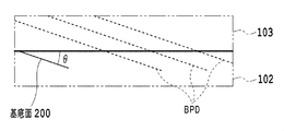
- FIG. 2 is a conceptual diagram showing a state in which basal plane dislocations (BPD) are propagated from the SiC substrate 102 of FIG. 1 to the epitaxial layer 103.
- BPD basal plane dislocations
- the SiC epitaxial layer 103 is crystal-grown (step flow growth) on the surface of the SiC substrate 102.
- the epitaxial layer 103 has a surface on which the step density is intentionally increased by tilting the SiC substrate 102 at an angle within 10 ° from the base surface 200 as a growth surface.
- the angle of the surface of SiC substrate 102 that is inclined with respect to base surface 200 is defined as off-angle ⁇ .
- Base plane is a general term for planes perpendicular to the C-axis of silicon carbide, and includes a (0001) plane (also referred to as “Si plane”) and a (000-1) plane (also referred to as “C plane”). . Also, a general term for the surface of silicon carbide that is perpendicular to the a-axis (axis perpendicular to the C-axis) (parallel to the C-axis) is referred to as “a-plane”. (2-1-10) plane, (-12-10) plane, (-2110) plane, (-1-120) plane, (1-210) plane, and the like.
- the stacking fault refers to a planar lattice defect formed by disordering the stacking order of crystal atomic planes.
- a typical example of the stacking fault is a single Shockley stacking fault (Single-Shockley-Stacking-Fault: SSF).
- SSF is a structure in which one layer of stacking faults is inserted in a 4H—SiC crystal (hexagonal structure composed of four layers) that is usually used in power semiconductors. Since SSF behaves like a quantum well in the ⁇ 0001> direction of 4H—SiC crystal, it captures and traps electrons.
- the stacking fault acts as a lifetime killer and thus increases the on-resistance.
- the SSF increases and the power semiconductor device has a high resistance, a phenomenon occurs in which the forward current decreases with time when the voltage is constant. Since SSF is generated and grows using BPD as a nucleus, reduction of BPD is indispensable in order to suppress the increase of SSF.
- Patent Document 1 In order to reduce the BPD of the epitaxial layer 103, two methods of “low off-angle growth during epitaxial film formation” and “KOH (potassium hydroxide) etching as a pretreatment for epitaxial growth” have been proposed (for example, non-epitaxial growth).
- KOH potassium hydroxide
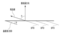
- W is the elastic energy at which the dislocation grows linearly
- E is the elastic energy of the defect
- ⁇ is the angle between the film growth direction and the dislocation line. Note that the film growth direction coincides with the normal direction of the surface of the substrate.
- FIG. 3A and 3B are diagrams for explaining a method of reducing basal plane dislocation (BPD) by an off angle.
- FIG. 3A shows a case where the off angle is large
- FIG. 3B shows a case where the off angle is small.
- W is smaller than the equation (1).
- the energy for extending the basal plane dislocation is reduced, so that the basal plane dislocation is easily grown in the epitaxial layer 103.
- step bunching is formed on the surface of the epitaxial layer 103.
- step bunching is an epitaxial growth process in which each atomic layer grows laterally with respect to its growth direction, so that the growth steps at the ends of each atomic layer are integrated under certain conditions. This is a phenomenon in which the unevenness of the surface of the epitaxial layer 103 becomes intense.
- the depth of KOH etching that does not grow BPD is as large as 7 ⁇ m. This corresponds to 70% of the film thickness of the 10 ⁇ m epitaxial layer 103 capable of 1.2 kV withstand voltage.
- Such local variations in film thickness cause a decrease in the breakdown voltage of the semiconductor device in the manufacture of the semiconductor device, and thus do not hold as a semiconductor device manufacturing process.
- the use of KOH results in alkaline contamination of the device. For these reasons, it is very difficult to apply the KOH etching process to the SiC substrate 102 before the epitaxial growth as an industrial process.
- An object of the present invention is to provide a semiconductor device in which crystal defects such as stacking faults are reduced by treating the surface of a SiC substrate before epitaxial growth.
- the present invention forms a periodic texture in a direction perpendicular to the ⁇ 1100> direction of the SiC substrate, and an angle formed between the base surface of the SiC substrate and the surface of the formed texture.
- An epitaxial film is formed on a SiC substrate having an angle smaller than the off-angle.
- the BPD density in the epitaxial film can be reduced, the number of stacking faults generated by energization can be suppressed, and the phenomenon that the forward current decreases with time when the voltage is constant can be suppressed.
- FIG. 1 is a configuration diagram showing an example of a conventional SiC_PN diode
- FIG. 2 is a conceptual diagram showing a state in which basal plane dislocation (BPD) propagates to the epitaxial layer
- FIG. 3A is a diagram for explaining a method of reducing basal plane dislocation (BPD) by an off angle, and shows a case where the off angle is large
- FIG. 3B is a diagram showing a case where the off-angle is small
- FIG. 4 is a view showing a method for producing an SiC substrate polishing material according to an embodiment of the present invention
- FIG. 5A is a diagram showing an abrasive according to an embodiment of the present invention
- FIG. 5B is a diagram showing a SiC substrate according to an embodiment of the present invention
- FIG. 6A is a diagram showing a method for processing an SiC substrate according to an embodiment of the present invention, and is a diagram showing a plan view of the processed SiC substrate
- FIG. 6B is a diagram showing a cross-sectional view of the SiC substrate along the AA ′ cross-sectional line in FIG. 6A
- FIG. 7A is a schematic diagram showing details of the surface shape of the SiC substrate before and after being processed by the method of processing an SiC substrate according to one embodiment of the present invention, and is a diagram showing the surface shape of the SiC substrate before processing
- FIG. 7B is a diagram showing the surface shape of the SiC substrate after processing
- FIG. 8 is a schematic diagram showing details of the texture formed on the surface of the SiC substrate according to the embodiment of the present invention
- FIG. 9 is a schematic diagram showing details of the texture formed on the surface of the SiC substrate according to another embodiment of the present invention
- FIG. 10 is a schematic diagram showing details of a texture formed on the surface of a SiC substrate according to another embodiment of the present invention
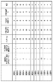
- FIG. 11 is a table showing the results of one example of the present invention and a comparative example
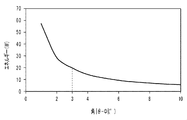
- FIG. 12 is a diagram showing a relationship between “elastic energy of BPD” and “angle formed by the base surface of the SiC substrate and the texture surface” according to an embodiment of the present invention.
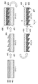
- FIG. 4 is a diagram showing a method for producing a polished material for a SiC substrate according to an embodiment of the present invention.
- Polishing workpiece 400 is a processing tool having a catalytic action and used for processing the surface shape of a SiC substrate.
- a Cr film 402 is formed on a glass substrate 401, and a resist 403 is applied on the Cr film 402.
- the Cr film 402 can be formed by vapor deposition, ion beam vapor deposition, sputtering, or the like, but it is preferable to use ion beam vapor deposition or sputtering because adhesion strength is weak only by vapor deposition.
- a resist corresponding to an electron beam such as OEBR-1OOO manufactured by Tokyo Ohka Kogyo Co., Ltd. can be used, and the film thickness is preferably 0.1 ⁇ m or more and 3 ⁇ m or less.
- the OEBR-1OOO given as an example is a positive type, but a negative type can also be used.
- step 2 resist patterning is performed in which the resist 403 is exposed by an electron beam dose variable method.
- an acceleration voltage in the range of 20-70 keV and a dose of 2 ⁇ C / cm 2 to 200 ⁇ C / cm 2 .
- the patterning is performed such that the cross section shown in FIG. 4 has a saw-tooth cross-sectional shape, and the apexes and valleys of the peaks are lines parallel to each other in the direction perpendicular to the paper surface. That is, when the polishing workpiece 400 is viewed from the resist 403 side, a line pattern composed of a plurality of parallel lines is formed.
- the dose amount is continuously changed in the direction perpendicular to the line, and the dose amount is constant in the direction along the line.
- annealing is performed at 150 ° C. for about 30 minutes, and the resist shape 404 with the controlled inclination angle ⁇ can be manufactured by performing resist stripping using a stripping agent suitable for the resist 403. In this way, a resist shape 404 corresponding to a desired line pattern and cross-sectional shape is formed.
- Step 3 is to form a Ni or NiP seed layer 405 by sputtering.
- the film thickness of the seed layer 405 is preferably about 100 nm.
- a Ni plate 406 is formed on the seed layer 405 by electroplating.
- the thickness of the Ni plate 406 is required to be 100 ⁇ m or more in order to give the strength not to be deformed by its own weight, and is preferably 700 ⁇ m or less because it is better from the viewpoint of manufacturing cost and man-hours.
- step 4 the Ni plate 406 is peeled from the resist-coated glass substrate 401 having a resist shape 404.
- a surface coat layer is formed.
- sputtering and ion coat deposition of Pt407 which is a surface coat layer, is performed in the range of 5 nm to 30 nm. This is because 5 nm or more is necessary to form a film uniformly and with good coverage, and 30 nm or less is necessary to prevent the pattern shape from being blurred.
- a polishing tool is formed such that the surface of the SiC substrate has a desired line pattern and cross-sectional shape (inclination angle ⁇ , depth d, pitch L).
- the difference between the off-angle ⁇ and the inclination angle ⁇ is preferably within 3 °.
- the depth d is preferably 15 nm or less, more preferably 10 nm or less.
- the depth d needs to be 3 nm or more from the viewpoint of stable quality and cost.
- the pitch L is 20 nm or more, preferably 200 nm or less, more preferably 100 nm or less from the viewpoint of stable quality and cost. If the pitch L is longer than 200 nm, good step-terrace growth is hindered and different polytypes grow. Further, when the pitch L is increased, steps are present in a stepped manner on the crystal surface, so that step bunching is easily caused during the crystal growth, in which these step sequences are combined to form a bundle and form a huge step.
- FIG. 5A shows an abrasive material according to one embodiment of the present invention
- FIG. 5B is a diagram showing a SiC substrate according to one embodiment of the present invention.
- the off-angle ⁇ of the 4H—SiC substrate 500 to be used is not limited to 4 °, and is preferably 0 ° or more and less than 10 °. If the off-angle of the 4H—SiC substrate 500 is 0 °, the surface of the 4H—SiC substrate 500 is parallel to the basal plane, so the direction of the BPD is also parallel to the surface of the 4H—SiC substrate 500.
- a liquid amount (3 cc or more) of hydrofluoric acid is dropped so as to spread over the entire surface of the 4H-SiC substrate 500.
- the polishing material 400 is pressurized so that it can uniformly contact the surface of the 4H—SiC substrate 500 in which hydrofluoric acid has spread.
- the entire surface of the polishing material 400 and the 4H-SiC substrate 500 is pressed by pressurizing at a total of 5 points or more of 4 points concentrically 1 cm inward from the center and outer periphery of the mold in 90 ° increments. Are preferably contacted evenly.
- the pressure is preferably 0.5 g / cm 2 or more and 200 g / cm 2 or less.
- the line pattern of the polishing workpiece 400 and the ⁇ 11-20> direction of the 4H—SiC crystal in the 4H—SiC substrate 500 are set in the vertical direction. That is, the line pattern and the ⁇ 1100> direction of the 4H—SiC crystal are set in parallel.
- the polishing material 400 is reciprocated with the direction parallel to the line pattern of the polishing material 400 as the processing direction.
- the reciprocating speed is preferably in the range of 1 mm / sec to 100 mm / sec.
- the surface coat layer Pt407 serves as a catalyst, and the surface of the 4H—SiC substrate 500 is polished without an abrasive. Since it is not physical processing but chemical processing using a catalytic action, once this abrasive workpiece 400 is produced, processing of 100 sheets or more is possible.
- the surface coat layer is not limited to Pt407, and noble metal materials such as Ir, Re, Pd, Rh, Os, Au, and Ag can be used. In addition, you may process by adding a diamond abrasive grain etc. and adding a mechanical effect
- the processing method of this embodiment By using the processing method of this embodiment and the 4H—SiC substrate 500 processed by the processing method, most of the region of the surface of the 4H—SiC substrate 500 before epitaxial growth can be made a low off-angle region. BPD which becomes the nucleus of defect growth can be reduced.
- the line pattern having a predetermined step and pitch and the cross-sectional shape may not be continuously formed on the entire surface of the 4H—SiC substrate (wafer) 500, or may be formed intermittently.
- a minute step formed on the surface of the 4H—SiC substrate 500 of this embodiment does not become an electric field concentration point that leads to deterioration of device characteristics.
- the 4H—SiC substrate 500 since the 4H—SiC substrate 500 has a large number of steps and a large number of epitaxial growth points, the growth rate of the epitaxial film is not greatly reduced from the conventional structure.
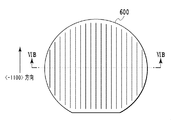
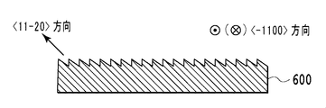
- FIG. 6A and 6B are diagrams showing a SiC substrate processed by the SiC substrate processing method according to an embodiment of the present invention.
- FIG. 6A shows a plan view of SiC substrate 600 after processing.
- FIG. 6B shows a cross-sectional view of SiC substrate 600 taken along the line AA ′ of FIG. 6A.
- a line pattern texture is formed on the surface of the SiC substrate 600 in the ⁇ 1100> direction of the 4H—SiC crystal in the SiC substrate 600.
- an inclination angle with respect to the surface of SiC substrate 600 is formed on the surface of SiC substrate 600 along the cross-sectional shape.
- 6B represents the ⁇ 11-20> direction perpendicular to the ⁇ 1100> direction of the 4H—SiC crystal.
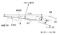
- FIG. 7A and 7B are schematic views showing details of the surface shape of the SiC substrate before and after being processed by the SiC substrate processing method according to one embodiment of the present invention.
- FIG. 7A is a diagram showing a surface shape of SiC substrate 600 before processing.
- a step-terrace structure is formed that is inclined from the basal plane 700 by an off angle ⁇ .
- the “surface” indicated by the dotted line is the surface when the wafer is viewed in a macro manner.
- the off-angle ⁇ is an angle from the base surface 700 of the SiC substrate 600 to the surface of the SiC substrate 600. From the above formula (1), when the off angle ⁇ is reduced, the propagation of BPD to the epitaxial layer is reduced. However, if the off angle ⁇ is small, step bunching is likely to occur. That is, the step of two-dimensional growth—terrace growth is hindered and three-dimensional growth occurs. Therefore, according to the processing method of the present embodiment, the difference between the inclination angle ⁇ from the surface of the SiC substrate 600 and the off-angle ⁇ of the SiC substrate 600 is smaller (within 3 °), and the periodic groove. Form.
- FIG. 7B is a diagram showing a surface shape of the SiC substrate 600 processed by the processing method of the present embodiment.
- a texture having a T plane inclined from the surface by an inclination angle ⁇ and an S plane inclined from the T plane by a valley angle ⁇ is formed.
- Inclination angle ⁇ is a case where the angle is smaller than off-angle ⁇ from base surface 700 of SiC substrate 600, but is not limited thereto, and may be an angle larger than off-angle ⁇ .
- the texture of SiC substrate 600 has a distance (pitch L) in a direction perpendicular to the ⁇ 1100> direction of SiC substrate 600 of the groove formed from the T plane and the S plane, and valleys from the surface of SiC substrate 600. It has a vertical distance (depth d) to the tangent line between the T plane and the S plane forming the angle ⁇ . Furthermore, the valley angle ⁇ is preferably 90 ° +
- the S-plane is parallel to the ⁇ 0001> C-axis direction, so that step-terrace growth is favorably performed.
- the T plane is referred to as a texture plane.
- FIG. 7B is a schematic diagram, and the scale is different. The step-terrace structure shown by the two-dot chain line is actually smaller than the solid line formed by the texture. When the T plane is viewed microscopically, it shows schematically a step-terrace structure like a two-dot chain line.
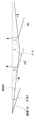
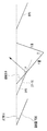
- FIG. 8 to 10 are schematic views showing details of the texture formed on the surface of the SiC substrate according to the embodiment of the present invention.
- FIG. 8 is a diagram showing a case where a texture having a T plane inclined from the surface of SiC substrate 600 by an inclination angle ⁇ smaller than the off angle ⁇ and an S plane inclined from the T plane by a valley angle ⁇ is formed. It is.
- the angle ⁇ between the normal direction of the T plane wider than the S plane and the dislocation line of the BPD is increased, the dislocation of the BPD is difficult to propagate to the epitaxial layer. Thereby, even if BPD hits the T-plane, BPD does not grow, and the growth of BPD can be reduced. Since the S plane is narrower than the T plane, the probability that BPD hits the S plane is small.
- FIG. 9 is a diagram showing a case where a texture having the same width of the T plane and the S plane is formed on the surface of the SiC substrate 600.
- the angles ⁇ and ⁇ between the normal direction of the T-plane and S-plane and the dislocation line of the BPD are both increased, the dislocation of the BPD is difficult to propagate to the epitaxial layer, and the growth of the BPD is reduced. Can do.
- FIG. 10 is a diagram showing a case where a texture having a T plane inclined from the surface of the SiC substrate 600 by an inclination angle ⁇ larger than the off angle ⁇ and an S plane inclined from the T plane by a valley angle ⁇ is formed. It is. Also in this case, as in FIG. 8, the angle ⁇ between the normal direction of the T-plane and the dislocation line of the BPD becomes large, so that the dislocation of the BPD is difficult to propagate to the epitaxial layer. Thereby, even if BPD hits the T-plane, BPD does not grow, and the growth of BPD can be reduced.
- the stacked dislocations can be reset, so that the propagation of BPD to the epitaxial film can be prevented.
- the characteristic is that the BPD dislocations are difficult to propagate to the epitaxial film if the angle (
- a SiC epitaxial film corresponding to the withstand voltage is formed on the processed SiC substrate 600.
- a film thickness of about 5 ⁇ m for a 600V breakdown voltage and a film thickness of about 10 ⁇ m for a 1200V breakdown voltage are sufficient. Since unevenness is generated on the surface of the SiC substrate 600 after the epitaxial film formation, a CMP process may be performed to flatten the surface. The flatness at this time is preferably 0.7 nm or less in terms of Ra. This is because if the unevenness is large, it becomes a leak point.
- SiC_PN diode By producing a SiC_PN diode by a well-known method using the SiC substrate 600 produced under the above conditions, it is possible to suppress the phenomenon that the forward current decreases with time when the voltage is constant without losing mass productivity. It becomes possible. Further, by using the manufacturing method of the present embodiment, mass production of high-quality and low-cost SiC_PN diodes and MOSFETs becomes possible.
- the processing of the surface shape of the SiC substrate is realized by the production of the polishing material and the processing method using the same, but the processing method of the surface shape is not limited thereto.
- FIG. 11 shows each dimension of the SiC substrate (an angle between the base surface and the textured surface, an inclination angle, and a pitch) and a SiC_PN diode manufactured with the dimensions, an initial reverse leakage good product rate, and a non-defective product with a forward voltage (Vf) deterioration. Rate, and the result of putting together the total non-defective product rate.
- the initial reverse leakage non-defective rate is a non-defective rate when the reverse leakage current when 1300 V is applied is 1 ⁇ A or less. Further, the non-defective product rate of forward voltage (Vf) degradation is 5% in a 125 ° C.
- the overall non-defective rate was 80% or more as a double circle, 70% or more and less than 80% as a circle, and less than 70% as a cross.
- the angle formed by the base surface of the SiC substrate and the textured surface is preferably 3 ° or less. From this result, it is expected that the probability that BPD which is the nucleus of the stacking fault is converted to TPD is increased, and BPD in the epitaxial film is decreased. Further, it has been found that the effect is obtained even when the inclination angle ⁇ is larger than the off angle ⁇ .
- the result of Comparative Example 2 in which the textured surface is parallel to the basal plane is considered to be that the yield rate decreased because the epitaxial growth on the basal plane hindered the growth of a two-dimensional epitaxial film.
- the pitch was preferably 200 nm or less, and more preferably 100 nm or less. This is because if the pitch is large, the growth of a two-dimensional epitaxial film is hindered, and it becomes difficult to maintain uniformity as an epitaxial film. If the pitch is 100 nm or less, the film quality is further improved and the film formation rate is increased. However, if the pitch is too small, the effect of resetting the BPD is diminished. In addition, since the depth becomes too small, the mold pattern is not accurately reflected on the SiC surface, and the overall yield rate decreases. Therefore, the pitch is preferably 30 nm or more, and more preferably 50 nm or more.
- FIG. 12 is a graph showing the relationship between “BPD elastic energy” and “angle between the base surface of the SiC substrate and the textured surface” according to an embodiment of the present invention.
- the vertical axis represents the elastic energy W at which the BPD grows linearly when the value of the elastic energy E of the extended defect in the above formula (1) is 1.
- the horizontal axis represents the angle
Landscapes
- Chemical & Material Sciences (AREA)
- Crystallography & Structural Chemistry (AREA)
- Engineering & Computer Science (AREA)
- Materials Engineering (AREA)
- Metallurgy (AREA)
- Organic Chemistry (AREA)
- Inorganic Chemistry (AREA)
- Chemical Kinetics & Catalysis (AREA)
- General Chemical & Material Sciences (AREA)
- Crystals, And After-Treatments Of Crystals (AREA)
- Recrystallisation Techniques (AREA)
Abstract
Description

本実施形態のSiC基板の表面形状の加工方法において、表面加工パターンを変更させた実験を行い、そのSiC基板を使用して耐圧1200VクラスのSiC_PNダイオードを作製した。
Claims (9)
- SiC基板の<-1100>方向に垂直な方向に周期的なテクスチャーを形成し、前記SiC基板の基底面と形成したテクスチャーの面とのなす角がオフ角より小さい前記SiC基板上に、エピタキシャル成膜することを特徴とする半導体の製造方法。
- 前記テクスチャーは、表面に表面コート層を有する加工工具と前記SiC基板とを接触させ、前記加工工具を前記SiC基板の<-1100>方向に往復運動させて形成されていることを特徴とする請求項1に記載の半導体の製造方法。
- 前記表面コート層は、Pt、Ir、Re、Pd、Rh、Os、AuおよびAgのいずれかであることを特徴とする請求項2に記載の半導体の製造方法。
- 前記SiC基板の基底面と前記形成したテクスチャーの面とのなす角が3°以内であることを特徴とする請求項1に記載の半導体の製造方法。
- 前記テクスチャーの前記SiC基板の<-1100>方向に垂直な方向のピッチが200nm以下であることを特徴とする請求項1に記載の半導体の製造方法。
- SiC基板の<-1100>方向に垂直な方向に周期的なテクスチャーが形成され、前記SiC基板の基底面と形成したテクスチャーの面とのなす角がオフ角より小さいことを特徴とするSiC基板。
- 前記SiC基板の基底面と前記形成したテクスチャーの面とのなす角が3°以内であることを特徴とする請求項6に記載のSiC基板。
- 前記テクスチャーの前記SiC基板の<-1100>方向に垂直な方向のピッチが200nm以下であることを特徴とする請求項6に記載のSiC基板。
- 前記テクスチャーの2つの面が作る谷角をΨ、前記SiC基板の表面から基底面までの角度をオフ角θ、および前記SiC基板の表面からの傾斜角をφとすると、前記谷角Ψが、
Ψ=90°+|θ-φ|
を満たすことを特徴とする請求項6に記載のSiC基板。
Priority Applications (4)
| Application Number | Priority Date | Filing Date | Title |
|---|---|---|---|
| DE112016000120.7T DE112016000120T5 (de) | 2015-04-17 | 2016-03-25 | Halbleiterherstellungsverfahren und SiC-Substrat |
| JP2017512191A JP6380663B2 (ja) | 2015-04-17 | 2016-03-25 | 半導体の製造方法およびSiC基板 |
| CN201680003021.6A CN106795649B (zh) | 2015-04-17 | 2016-03-25 | 半导体的制造方法以及SiC基板 |
| US15/476,327 US10246793B2 (en) | 2015-04-17 | 2017-03-31 | Semiconductor manufacturing method and SiC substrate |
Applications Claiming Priority (2)
| Application Number | Priority Date | Filing Date | Title |
|---|---|---|---|
| JP2015-085449 | 2015-04-17 | ||
| JP2015085449 | 2015-04-17 |
Related Child Applications (1)
| Application Number | Title | Priority Date | Filing Date |
|---|---|---|---|
| US15/476,327 Continuation US10246793B2 (en) | 2015-04-17 | 2017-03-31 | Semiconductor manufacturing method and SiC substrate |
Publications (1)
| Publication Number | Publication Date |
|---|---|
| WO2016166939A1 true WO2016166939A1 (ja) | 2016-10-20 |
Family
ID=57127238
Family Applications (1)
| Application Number | Title | Priority Date | Filing Date |
|---|---|---|---|
| PCT/JP2016/001742 Ceased WO2016166939A1 (ja) | 2015-04-17 | 2016-03-25 | 半導体の製造方法およびSiC基板 |
Country Status (5)
| Country | Link |
|---|---|
| US (1) | US10246793B2 (ja) |
| JP (1) | JP6380663B2 (ja) |
| CN (1) | CN106795649B (ja) |
| DE (1) | DE112016000120T5 (ja) |
| WO (1) | WO2016166939A1 (ja) |
Families Citing this family (3)
| Publication number | Priority date | Publication date | Assignee | Title |
|---|---|---|---|---|
| EP3642847A1 (en) | 2018-08-31 | 2020-04-29 | Google LLC. | Privacy-first on-device federated health modeling and intervention |
| FR3118284B1 (fr) * | 2020-12-17 | 2022-11-04 | Commissariat Energie Atomique | Dispositif électronique en siliciure de carbone et son procédé de fabrication |
| TWI897309B (zh) * | 2024-03-21 | 2025-09-11 | 鴻揚半導體股份有限公司 | 半導體結構及其製造方法 |
Citations (4)
| Publication number | Priority date | Publication date | Assignee | Title |
|---|---|---|---|---|
| JP2007182330A (ja) * | 2004-08-24 | 2007-07-19 | Bridgestone Corp | 炭化ケイ素単結晶ウェハ及びその製造方法 |
| JP2008311541A (ja) * | 2007-06-18 | 2008-12-25 | Fuji Electric Device Technology Co Ltd | 炭化珪素半導体基板の製造方法 |
| JP2010184829A (ja) * | 2009-02-12 | 2010-08-26 | Denso Corp | 炭化珪素単結晶の製造方法 |
| JP2012153543A (ja) * | 2011-01-21 | 2012-08-16 | Central Research Institute Of Electric Power Industry | 炭化珪素単結晶の製造方法、炭化珪素単結晶ウエハ、炭化珪素半導体素子の製造方法、炭化珪素半導体素子 |
Family Cites Families (12)
| Publication number | Priority date | Publication date | Assignee | Title |
|---|---|---|---|---|
| JP2768988B2 (ja) * | 1989-08-17 | 1998-06-25 | 三菱電機株式会社 | 端面部分コーティング方法 |
| TW518767B (en) * | 2000-03-31 | 2003-01-21 | Toyoda Gosei Kk | Production method of III nitride compound semiconductor and III nitride compound semiconductor element |
| US7173285B2 (en) | 2004-03-18 | 2007-02-06 | Cree, Inc. | Lithographic methods to reduce stacking fault nucleation sites |
| US7109521B2 (en) | 2004-03-18 | 2006-09-19 | Cree, Inc. | Silicon carbide semiconductor structures including multiple epitaxial layers having sidewalls |
| JP4628189B2 (ja) * | 2005-06-07 | 2011-02-09 | Hoya株式会社 | 炭化珪素単結晶の製造方法 |
| JP4769541B2 (ja) * | 2005-10-27 | 2011-09-07 | トヨタ自動車株式会社 | 半導体材料の製造方法 |
| JP4959763B2 (ja) * | 2009-08-28 | 2012-06-27 | 昭和電工株式会社 | SiCエピタキシャルウェハ及びその製造方法 |
| JP2013049609A (ja) * | 2011-08-31 | 2013-03-14 | Rohm Co Ltd | SiCエピタキシャルウエハおよびそれを用いたSiC半導体素子 |
| JP5961357B2 (ja) * | 2011-09-09 | 2016-08-02 | 昭和電工株式会社 | SiCエピタキシャルウェハ及びその製造方法 |
| US9988738B2 (en) | 2013-02-13 | 2018-06-05 | Mitsubishi Electric Corporation | Method for manufacturing SiC epitaxial wafer |
| JP6057292B2 (ja) * | 2013-06-13 | 2017-01-11 | 学校法人関西学院 | SiC半導体素子の製造方法 |
| US9627199B2 (en) * | 2013-12-13 | 2017-04-18 | University Of Maryland, College Park | Methods of fabricating micro- and nanostructure arrays and structures formed therefrom |
-
2016
- 2016-03-25 CN CN201680003021.6A patent/CN106795649B/zh active Active
- 2016-03-25 DE DE112016000120.7T patent/DE112016000120T5/de not_active Withdrawn
- 2016-03-25 JP JP2017512191A patent/JP6380663B2/ja active Active
- 2016-03-25 WO PCT/JP2016/001742 patent/WO2016166939A1/ja not_active Ceased
-
2017
- 2017-03-31 US US15/476,327 patent/US10246793B2/en active Active
Patent Citations (4)
| Publication number | Priority date | Publication date | Assignee | Title |
|---|---|---|---|---|
| JP2007182330A (ja) * | 2004-08-24 | 2007-07-19 | Bridgestone Corp | 炭化ケイ素単結晶ウェハ及びその製造方法 |
| JP2008311541A (ja) * | 2007-06-18 | 2008-12-25 | Fuji Electric Device Technology Co Ltd | 炭化珪素半導体基板の製造方法 |
| JP2010184829A (ja) * | 2009-02-12 | 2010-08-26 | Denso Corp | 炭化珪素単結晶の製造方法 |
| JP2012153543A (ja) * | 2011-01-21 | 2012-08-16 | Central Research Institute Of Electric Power Industry | 炭化珪素単結晶の製造方法、炭化珪素単結晶ウエハ、炭化珪素半導体素子の製造方法、炭化珪素半導体素子 |
Also Published As
| Publication number | Publication date |
|---|---|
| CN106795649A (zh) | 2017-05-31 |
| CN106795649B (zh) | 2019-12-17 |
| JPWO2016166939A1 (ja) | 2017-08-31 |
| DE112016000120T5 (de) | 2017-07-06 |
| US20170204531A1 (en) | 2017-07-20 |
| JP6380663B2 (ja) | 2018-08-29 |
| US10246793B2 (en) | 2019-04-02 |
Similar Documents
| Publication | Publication Date | Title |
|---|---|---|
| JP7637698B2 (ja) | 窒化物エピタキシャルウェーハ、その製造方法、および半導体デバイス | |
| JP6090998B2 (ja) | 六方晶単結晶の製造方法、六方晶単結晶ウエハの製造方法 | |
| JP6904774B2 (ja) | 炭化珪素エピタキシャルウェハ、炭化珪素絶縁ゲート型バイポーラトランジスタ及びこれらの製造方法 | |
| US20110006310A1 (en) | Semiconductor device and semiconductor device manufacturing method | |
| US20080318359A1 (en) | Method of manufacturing silicon carbide semiconductor substrate | |
| US20140361337A1 (en) | Semiconductor Device and Method for Manufacturing Semiconductor Device | |
| US9988738B2 (en) | Method for manufacturing SiC epitaxial wafer | |
| JP6123408B2 (ja) | 単結晶4H−SiC基板及びその製造方法 | |
| JP2018142655A (ja) | ショットキーバリアダイオード | |
| EP4044212B1 (en) | Semiconductor substrate, manufacturing method therefor, and semiconductor device | |
| US10892159B2 (en) | Semipolar or nonpolar group III-nitride substrates | |
| JP2013258251A (ja) | ショットキーバリアダイオードおよびその製造方法 | |
| JP6380663B2 (ja) | 半導体の製造方法およびSiC基板 | |
| JP2010192555A (ja) | ショットキバリアダイオードおよびその製造方法 | |
| US10508361B2 (en) | Method for manufacturing semiconductor wafer | |
| JP6269368B2 (ja) | 窒化ガリウム基板 | |
| JP2018536618A (ja) | 結晶基板上で半極性窒化層を得る方法 | |
| JP2012054427A (ja) | 化合物半導体の製造方法 | |
| CN104701385A (zh) | 纳米晶嵌入单晶外延碳化硅的高稳定低损耗微波二极管 | |
| JP6338490B2 (ja) | 炭化珪素エピタキシャルウエハ、炭化珪素半導体装置および炭化珪素エピタキシャルウエハの製造方法 | |
| WO2016002801A1 (ja) | 半導体積層構造体及び半導体素子 | |
| JP2025070005A (ja) | 窒化物結晶基板の製造方法、および窒化物結晶基板 | |
| JP4786587B2 (ja) | Iii族窒化物半導体およびその製造方法、iii族窒化物半導体製造用基板 | |
| US12106959B2 (en) | Nonpolar or semipolar group III-nitride substrates | |
| US20190067421A1 (en) | Semiconductor device and method of manufacturing semiconductor device |
Legal Events
| Date | Code | Title | Description |
|---|---|---|---|
| 121 | Ep: the epo has been informed by wipo that ep was designated in this application |
Ref document number: 16779738 Country of ref document: EP Kind code of ref document: A1 |
|
| WWE | Wipo information: entry into national phase |
Ref document number: 112016000120 Country of ref document: DE |
|
| ENP | Entry into the national phase |
Ref document number: 2017512191 Country of ref document: JP Kind code of ref document: A |
|
| 122 | Ep: pct application non-entry in european phase |
Ref document number: 16779738 Country of ref document: EP Kind code of ref document: A1 |