WO2016166805A1 - 荷電粒子線装置及び試料観察方法 - Google Patents
荷電粒子線装置及び試料観察方法 Download PDFInfo
- Publication number
- WO2016166805A1 WO2016166805A1 PCT/JP2015/061407 JP2015061407W WO2016166805A1 WO 2016166805 A1 WO2016166805 A1 WO 2016166805A1 JP 2015061407 W JP2015061407 W JP 2015061407W WO 2016166805 A1 WO2016166805 A1 WO 2016166805A1
- Authority
- WO
- WIPO (PCT)
- Prior art keywords
- image
- diaphragm
- unit
- charged particle
- particle beam
- Prior art date
- Legal status (The legal status is an assumption and is not a legal conclusion. Google has not performed a legal analysis and makes no representation as to the accuracy of the status listed.)
- Ceased
Links
Images







Classifications
-
- H—ELECTRICITY
- H01—ELECTRIC ELEMENTS
- H01J—ELECTRIC DISCHARGE TUBES OR DISCHARGE LAMPS
- H01J37/00—Discharge tubes with provision for introducing objects or material to be exposed to the discharge, e.g. for the purpose of examination or processing thereof
- H01J37/02—Details
- H01J37/04—Arrangements of electrodes and associated parts for generating or controlling the discharge, e.g. electron-optical arrangement or ion-optical arrangement
- H01J37/09—Diaphragms; Shields associated with electron or ion-optical arrangements; Compensation of disturbing fields
-
- H—ELECTRICITY
- H01—ELECTRIC ELEMENTS
- H01J—ELECTRIC DISCHARGE TUBES OR DISCHARGE LAMPS
- H01J37/00—Discharge tubes with provision for introducing objects or material to be exposed to the discharge, e.g. for the purpose of examination or processing thereof
- H01J37/02—Details
- H01J37/22—Optical, image processing or photographic arrangements associated with the tube
- H01J37/224—Luminescent screens or photographic plates for imaging; Apparatus specially adapted therefor, e. g. cameras, TV-cameras, photographic equipment or exposure control; Optical subsystems specially adapted therefor, e. g. microscopes for observing image on luminescent screen
-
- H—ELECTRICITY
- H01—ELECTRIC ELEMENTS
- H01J—ELECTRIC DISCHARGE TUBES OR DISCHARGE LAMPS
- H01J37/00—Discharge tubes with provision for introducing objects or material to be exposed to the discharge, e.g. for the purpose of examination or processing thereof
- H01J37/26—Electron or ion microscopes; Electron or ion diffraction tubes
-
- H—ELECTRICITY
- H01—ELECTRIC ELEMENTS
- H01J—ELECTRIC DISCHARGE TUBES OR DISCHARGE LAMPS
- H01J37/00—Discharge tubes with provision for introducing objects or material to be exposed to the discharge, e.g. for the purpose of examination or processing thereof
- H01J37/26—Electron or ion microscopes; Electron or ion diffraction tubes
- H01J37/261—Details
- H01J37/265—Controlling the tube; circuit arrangements adapted to a particular application not otherwise provided, e.g. bright-field-dark-field illumination
-
- H—ELECTRICITY
- H01—ELECTRIC ELEMENTS
- H01J—ELECTRIC DISCHARGE TUBES OR DISCHARGE LAMPS
- H01J37/00—Discharge tubes with provision for introducing objects or material to be exposed to the discharge, e.g. for the purpose of examination or processing thereof
- H01J37/26—Electron or ion microscopes; Electron or ion diffraction tubes
- H01J37/295—Electron or ion diffraction tubes
-
- H—ELECTRICITY
- H01—ELECTRIC ELEMENTS
- H01J—ELECTRIC DISCHARGE TUBES OR DISCHARGE LAMPS
- H01J2237/00—Discharge tubes exposing object to beam, e.g. for analysis treatment, etching, imaging
- H01J2237/04—Means for controlling the discharge
- H01J2237/045—Diaphragms
- H01J2237/0455—Diaphragms with variable aperture
Definitions
- the present invention relates to a charged particle beam apparatus and a sample observation method using the apparatus.
- TEM transmission electron microscope
- the present invention adopts the configuration described in the claims. That is, the present invention includes a display unit that displays an image, and a selection unit that selects a position of a predetermined portion from the displayed image, and according to the selection position of the predetermined portion, A configuration is employed in which a predetermined opening is selected from the positional relationship.
- the present invention relates to an irradiation unit that irradiates a sample with a charged particle beam, an imaging unit that forms an image of the sample, and an electron beam from the sample that is disposed in the imaging unit.
- a diaphragm formed with a plurality of apertures of different sizes for passing, a moving unit that changes the position of the diaphragm, a detection unit that obtains an image formed by the imaging optical system, and the detection unit
- a display unit that displays the obtained image, and a selection unit that selects a predetermined portion from the displayed image, and the moving unit is configured to select the diaphragm according to a selection position of the predetermined portion.
- the diaphragm is moved from a positional relationship with the image, and the image is at least one of an electron beam diffraction image and a transmission image of the sample, and the diaphragm is an objective that can be inserted into a diffraction surface in the imaging unit. At least a stop and a limited field stop that can be inserted into the primary image plane in the imaging unit It is one, a charged particle beam device.
- the operator can easily and automatically acquire a transmission image corresponding to the selected portion by selecting a predetermined portion (for example, a spot) of the diffraction image on the display unit, for example. it can. Further, according to the present invention, the operator can easily and automatically acquire a diffraction image corresponding to the selected portion by selecting a predetermined portion (for example, a range) of the transmission image on the display unit, for example. be able to. Problems, configurations, and effects other than those described above will become apparent from the following description of embodiments.
- the figure explaining the method of calibrating the moving pulse number of a diaphragm from a diffraction pattern.
- the figure which shows an example of GUI used when acquiring the diffraction pattern corresponding to the arbitrary ranges of a dark field image automatically.
- the flowchart explaining the method of acquiring automatically the diffraction pattern corresponding to the arbitrary ranges of a dark field image.
- FIG. 1 shows a schematic configuration example of a transmission electron microscope (TEM) which is one of charged particle beam apparatuses.
- TEM transmission electron microscope
- the electron beam generated by the electron gun 101 is focused by irradiation lenses 1 to 3 (102 to 104) and irradiated to a sample (not shown) mounted on the sample stage 105.
- the electrons that have passed through the sample are guided to the imaging surface of the CCD camera 114 via the imaging lenses 1 to 4 (110 to 113).
- the electronic image detected by the CCD camera 114 is imaged after being taken into the main controller 121. The operator observes this image as a sample image.
- the irradiation lenses 1 to 3 (102 to 104), the sample stage 105, the objective aperture 106, and the limited field stop 107 are controlled by an aperture control board 120 that receives a command from the main controller 121.
- the image imaged by the main control device 121 is displayed on the display device 123.
- the input device 124 is used to designate a partial region of the image displayed on the display device 123.
- a pointing device 180 described later is an example of the input device 124.
- the interior of the mirror body 100 is evacuated to about 10 ⁇ 5 Pa by an unillustrated evacuation pump.
- Specimens used for observation are sliced down to the order of several tens of nanometers with a focused ion beam device and mounted on a sample stage.
- the sample stage is attached to the sample holder, and is introduced into the mirror body 100 through a preliminary exhaust chamber (air lock chamber) incorporated in a sample moving device (not shown).
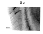
- FIG. 3 is an example of a TEM image (transmission image) taken using the CCD camera 114.
- FIG. 4 is an example of a diffraction pattern corresponding to a TEM image. On the image photographed by the CCD camera 114, a diffraction pattern (diffraction spot 201, transmission spot 202) corresponding to the crystal orientation of the sample is observed.
- the objective aperture 106 is installed in the vicinity of the region where the diffraction spot 201 is imaged.
- the objective aperture 106 is used to cut off scattered electrons that are not necessary when observing a TEM image (transmission image) or to capture an image (dark field image) formed by imaging only a specific diffraction spot 201.
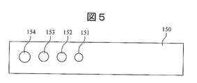
- a diaphragm plate 150 shown in FIG. 5 is attached to the tip of the objective diaphragm drive mechanism.
- a plurality of holes 151 to 154 having different diameters in the range of several ⁇ m to several 100 ⁇ m are provided.
- a diaphragm plate 150 having a mechanism capable of changing the diameter of the hole can also be used.
- the objective aperture driving mechanism moves the aperture plate 150 two-dimensionally in a plane orthogonal to the optical axis of the electron beam.
- a DC motor or a stepping motor (not shown) connected to the diaphragm control board 120 is appropriately selected.
- Example 1 the operation (Example 1) for photographing a TEM image (transmission image) using a transmission electron microscope and the operation (Example 2) for photographing a diffraction pattern (diffraction image) will be described separately.
- the operation described below can also be applied to the case where a TEM image (transmission image) or a diffraction pattern (diffraction image) is taken using various charged particle beam devices including an ion microscope.
- Example 1 an observation mode for automatically acquiring a dark field image corresponding to an arbitrary diffraction spot constituting a diffraction pattern will be described.
- a diffraction pattern and a transmission image are used.
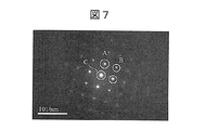
- the diffraction pattern shown in FIG. 7 includes transmitted waves and diffracted waves.
- a spot C in FIG. 7 corresponds to a transmitted wave, and the others are diffracted waves.
- An observation image formed using only the diffracted wave is a dark field image, and an observation image formed using only the transmitted wave is a bright field image.
- the dark field image and the bright field image are collectively referred to as a transmission image.
- the observation image is selected by selecting which diffraction spot is transmitted by the objective aperture 106.
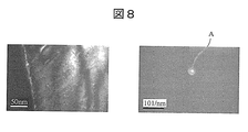
- the field of view becomes dark. That is, as shown in the right diagram of FIG. 8, only the electron beam that has passed through the objective aperture 106 can be observed. As can be seen from FIG. 8, there is at most one diffraction spot that has passed through the objective aperture 106. Therefore, it is very difficult to search for an arbitrary diffraction spot from the observed image.
- FIG. 10 is an example of a GUI displayed on the display device 123.
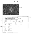
- a diffraction pattern is displayed in the image display area 400, and a GUI screen 401 is displayed below the diffraction pattern.
- FIGS. 10 and 11 a specific example of a function for automatically and continuously capturing dark field images corresponding to arbitrarily designated diffraction spots will be described.
- Step 1101 When it is desired to capture a dark field image corresponding to an arbitrary spot in the diffraction pattern to be observed, the operator switches the mode selection field 402 on the GUI screen 401 to the diffraction pattern observation mode. By this selection, a diffraction pattern is displayed in the image display area 400. The operator selects a diffraction spot at an arbitrary position where a dark field image is desired to be captured on the displayed diffraction pattern.
- the operator checks the A column of the check box 406 displayed on the GUI screen 401, clicks the registration button 403, and further clicks the spot A in the diffraction pattern. .
- a pointing device 180 or the like is used for the click operation here.
- the designation of the diffraction spot is not limited to one and may be plural.
- the operator checks the B column of the check box 406 displayed on the GUI screen 401, clicks the registration button 403, and further performs diffraction. Click spot B in the pattern. The click operation by the operator is repeatedly executed until registration of the spot to be photographed is completed. In FIG. 12, up to spot C is registered.
- Step 1102 Each time a diffraction spot is designated, main controller 121 selects a hole (any one of holes 151 to 154 constituting diaphragm plate 150) having an aperture diameter suitable for observing each diffraction spot.
- the selection of the aperture hole here is not limited to the case where an aperture having a size approximately equal to the size of any specified diffraction spot is selected as the optimum diameter, but the specified arbitrary diffraction spot is selected as a part of the aperture hole. This includes the case where the optimum diameter is selected.
- Step 1103 The main controller 121 calculates the coordinates of all the diffraction spots selected on the screen. A diffraction spot to be imaged is uniquely specified by the coordinates. This coordinate gives the position at which the objective stop is to be moved.
- Step 1104 The main controller 121 stores the calculated coordinates of one or more diffraction spots in a memory (not shown). That is, main controller 121 registers the calculated coordinates in the memory. Thereafter, the main controller 121 shifts to an operation mode for sequentially acquiring one or more stored dark field images of diffraction spots. Acquisition of a dark field image is started when the operator clicks the TEM button 404 using the pointing device 180.
- Step 1105 The main controller 121 that detects the click of the TEM button 404 first sets a specific hole (the hole selected in step 1102) of the objective aperture 106 for capturing a dark field image of the diffraction spot A, and coordinates of the diffraction spot A. Automatically move to position. That is, the position of the objective aperture 106 is adjusted so that the diffraction spot A and a specific hole of the objective aperture 106 coincide.
- the movement of the objective aperture 106 is controlled according to the positional relationship between the objective aperture 106 and the diffraction pattern. Note that the center of the objective aperture coincides with the center of the optical axis at the time of calibration described later. By matching both centers, the coordinate system of the camera image, the coordinate system of the image plane (primary image plane), and the coordinate system of the diffractive surface are similar, and these can be handled as one coordinate system. Become.
- Step 1106 When the operator clicks the shooting button 405, the main control device 121 switches the current value of the imaging lens to the TEM image observation mode to acquire the dark field image A of the diffraction spot A, and the image display area 400 of the display device 123. To display. The operator observes the dark field image A displayed in the image display area 400. If the number of designated diffraction spots is only one, the process ends in this step.
- Step 1107 If a plurality of diffraction spots are registered for taking a dark field image in step 1101, the main controller 121 automatically executes the dark field image taking process in order for the other diffraction spots.
- a specific hole (the hole selected in step 1102) of the objective aperture 106 for photographing the diffraction spot B is moved to the coordinate position of the diffraction spot B. That is, the position of the objective aperture 106 is adjusted so that the diffraction spot B and a specific hole of the objective aperture 106 coincide.
- the main controller 121 may switch the observation mode to the diffraction pattern observation mode. However, since the coordinates of the diffraction spot B are already registered, the main control device 121 may remain in the TEM image observation mode.
- Step 1108 When the operator clicks the shooting button 405, the main controller 121 acquires a dark field image B corresponding to the diffraction spot B and displays it in the image display area 400 of the display device 123. The operator observes the dark field image B displayed in the image display area 400. Steps 1107 and 1108 are repeatedly executed for all registered diffraction spots.
- the method of this embodiment by registering a plurality of diffraction spots in advance for one diffraction pattern, a plurality of dark field images corresponding to each diffraction spot can be automatically and continuously acquired. That is, in the method of this embodiment, unlike the conventional method, there is no need to repeat the operation of acquiring the dark field image by manually specifying the coordinate value of one diffraction spot for one diffraction pattern. For this reason, the method of the present embodiment can significantly improve the dark field image acquisition and the observation efficiency as compared with the conventional method.
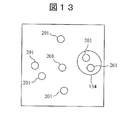
- FIG. 13 shows an example of the selection method.
- two diffraction spots 201 in the vicinity are designated.
- the hole 154 is used for observing dark field images corresponding to these two diffraction spots 201.
- the acquired dark field image is an image obtained by combining the individual dark field images of the two diffraction spots 201, and a dark field image with a high contrast ratio can be obtained.
- the drive mechanism has an X-axis motor 300 and a Y-axis motor 301 so that the objective aperture 106 can be moved two-dimensionally in a plane orthogonal to the optical axis of the electron beam. Further, the rotational force of the motor is transmitted to the linear movement of the movable shaft 306 by the gears and the feed screws 302 to 305. In order to perform high-precision control, the actual movement amount in the vicinity of the aperture is measured using the X-axis linear scale 307, and the measurement result is fed back to the motor control unit.
- the linear scales 308 to 309 are similarly mounted on the Y axis. This compares the target distance with the actual moving distance in the vicinity of the diaphragm plate 150 in order to minimize the influence of gear backlash and axial deformation.
- TEM the inside of the mirror body 100 into which the diaphragm plate 150 is inserted is evacuated. For this reason, a linear scale is installed inside the housing 100. As a result, even if a mechanical shift such as backlash occurs, accurate correction can be performed.
- an encoder, a gyro sensor, or the like can be considered as the motor control unit. However, in order to perform measurement including disturbance, it is desirable to measure the movement amount of the shaft.
- the coordinates of the diaphragm are calibrated by matching the diaphragm center with the camera center (optical axis center).
- the coordinates of the diaphragm mechanism with respect to the center of the optical axis, it is possible to calculate the shift amount when the observation region is selected on the GUI and to move to an arbitrary region.
- FIG. 14 shows an example of a diffraction pattern formed in the vicinity of the objective aperture 106.
- the diffraction pattern is formed with a plurality of diffraction spots on a plane perpendicular to the charged particle beam.
- the diffraction pattern is enlarged using an imaging lens, imaged on the scintillator of the CCD camera 114, and displayed on the screen of the display device 123.
- By driving a motor provided in the objective aperture driving mechanism it is possible to pass through the aperture hole only for an arbitrary spot.
- This correlation can be obtained by measuring the distance on the screen of the display device 123 when the aperture is moved by an amount corresponding to a certain number of pulses. For example, when the aperture hole is moved by P pulses, when moving the distance M on the screen of the display device 123, the movement amount per pulse can be obtained by M / P. Thus, for example, when the transmission spot 201 located at the center of the diffraction pattern is used as a reference and the distance on the display device 123 to the diffraction spot A is L, the aperture hole is moved to the position of the diffraction spot A. The number of pulses necessary for the calculation can be obtained by L ⁇ P / M.
- one or a plurality of diffraction spots to be observed are designated at a time within the same screen among a plurality of diffraction spots constituting one diffraction pattern.
- the dark field image corresponding to the designated diffraction spot can be acquired automatically. As a result, it is possible to significantly reduce the labor and work amount of the operator for observing the dark field image.
- Example 2 In the present embodiment, an observation mode for automatically acquiring a diffraction pattern corresponding to a partial region constituting a transmission image will be described.
- a transmission image formed by the objective lens is formed in a region below the sample.
- a limited field stop 107 is attached to this region.
- the limited field stop 107 is used to acquire a diffraction pattern of a specific region of the transmission image.
- the aperture plate constituting the limited field stop 107 is provided with a plurality of holes having a diameter of about 0.1 ⁇ m to several 100 ⁇ m, like the aperture plate 150 shown in FIG.
- the diffraction pattern formed immediately below the sample is enlarged and imaged on the CCD camera 114, or the TEM image formed by the objective lens is enlarged. Whether to form an image on the CCD camera 114 can be switched.
- the limited field stop 107 When the limited field stop 107 is inserted into the TEM image formed by the objective lens, only electrons in a specific region of the TEM image can be passed. Furthermore, when the observation mode is switched to the diffraction pattern observation mode by changing the current flowing through the imaging lenses 110 to 113, only the diffraction pattern corresponding to a specific region can be observed. Analysis of the atomic structure of a specific region is possible from this diffraction pattern.
- FIG. 15 is an example of a GUI displayed on the display device 123.
- a transmission image is displayed in the image display area 400, and a GUI screen 401 is displayed below it.
- a specific example of a function for automatically and continuously photographing diffraction patterns corresponding to individual selection ranges (partial regions) will be described with reference to FIGS. 15 and 16.
- Step 1601 When it is desired to capture a diffraction pattern corresponding to an arbitrary range in the transmission image to be observed, the operator switches the selection in the mode selection field 402 on the GUI screen 401 to the TEM image observation mode. Upon receiving this selection, the main controller 121 controls the imaging lenses 110 to 113 with a current suitable for the TEM image observation mode. As a result, a TEM image is displayed in the image display area 400.
- Step 1602 The operator selects an arbitrary range from the TEM images displayed in the image display area 400. For example, when selecting the selection range A, the operator checks the A column of the check box 406 displayed on the GUI screen 401, clicks the registration button 403, and further, observes an arbitrary range observed in the TEM image. A is specified. The designation (selection) of the range here is performed by clicking or dragging the pointing device.
- the selection of the range is not limited to one, but may be multiple.
- the operator checks the B column of the check box 406 displayed on the GUI screen 401, clicks the registration button 403, and further selects an arbitrary selection range B of the diffraction pattern. specify.
- the range designation operation by the operator is repeatedly executed until registration of the range to be photographed is completed.
- Step 1603 Each time the range is designated (selected), main controller 121 selects a diaphragm diameter corresponding to the size.
- the aperture diameter here is a diameter of a hole constituting the limited field stop 107.
- Step 1604 Each time the range is designated (selected), main controller 121 calculates its center coordinates and stores the coordinates in memory. If the size of the range is arbitrary, the size of the range is also stored in the memory. Thereafter, the main controller 121 shifts to an operation mode in which diffraction patterns corresponding to one or more stored ranges are sequentially acquired. Acquisition of the diffraction pattern is started when the operator clicks the diffraction pattern button 407 using the pointing device 180.
- Step 1605 the main controller 121 automatically moves a specific hole (the hole selected in step 1603) of the limited field stop 107 to the coordinate position of the range A. That is, the position of the limited field stop 107 is adjusted so that the range to be structurally analyzed matches a specific hole of the limited field stop 107.
- the movement of the restricted field stop 107 is determined according to the positional relationship between the restricted field stop 107 and the TEM image.
- the center of the limited field stop and the center of the optical axis coincide. By matching both centers, the coordinate system of the camera image, the coordinate system of the image plane (primary image plane), and the coordinate system of the diffractive surface are similar, and these can be handled as one coordinate system. Become.
- Step 1606 When the imaging button 405 is clicked, the main controller 121 switches the current value of the imaging lens to the diffraction pattern observation mode, acquires the diffraction pattern A corresponding to the selection range A, and displays the image display area 400 of the display device 123. To display. The operator observes the diffraction pattern A displayed in the image display area 400. If the number of designated diffraction spots is only one, the process ends in this step.
- Step 1607 If a plurality of selected ranges are registered for photographing the diffraction pattern in step 1601, the main control device 121 automatically executes the diffraction pattern photographing processing in order for the other ranges.
- a specific hole (the hole selected in step 1603) of the limited field stop 107 for photographing the selection range B is moved to the coordinate position of the selection range B.
- main controller 121 may switch the observation mode to the TEM image observation mode.
- the coordinates of selection range B have already been registered, it may remain in the diffraction pattern observation mode.
- Step 1608 When the photographing button 405 is clicked, the main controller 121 switches the current value of the imaging lens to the diffraction pattern observation mode, acquires the diffraction pattern B in the selection range B, and displays it in the image display area 400 of the display device 123. To do. The operator observes the diffraction pattern B displayed in the image display area 400. Steps 1607 and 1608 are repeatedly executed for all registered diffraction spots.
- a plurality of diffraction patterns corresponding to each selection range can be automatically and continuously acquired. That is, unlike the conventional method, there is no need to repeat the operation of acquiring a diffraction pattern by specifying one range for one TEM image, and the method of this embodiment improves the acquisition of the diffraction pattern and the observation efficiency conventionally. Compared with the method, the efficiency can be significantly improved.
- crystal structure analysis such as crystal orientation and crystal grain bond angle can be performed. These analyzes can also be performed at once on a plurality of acquired diffraction patterns.
- the operator can select a specific diffraction pattern and move to the diffraction pattern.
- the operator can easily acquire the diffraction patterns of multiple observation objects in a short time, and can select the TEM image corresponding to an arbitrary range by holding the coordinates corresponding to the acquired diffraction patterns in the memory. Can also be observed.
- the acquired diffraction pattern and its coordinates can be stored for the sample position where the diffraction pattern is acquired.
- the limited field stop 107 in this embodiment also has a drive mechanism similar to the objective stop drive mechanism shown in FIG.
- the movement accuracy can be improved by arranging a linear scale in each of the X-axis direction and the Y-axis direction, measuring the actual movement amount in the vicinity of the diaphragm, and feeding back the measurement result to the motor control unit.
- the positional relationship of the drive mechanism of the limited field stop 107 is calibrated in advance by the same procedure as that of the objective stop drive mechanism. For example, if you count the number of pulses required to move between the two setting ranges specified on the display screen (one is preferably set near the center of the screen), the number of pulses required for each movement Can be calculated.
- this invention is not limited to an above-described Example, Various modifications are included.
- the above-described embodiments have been described in detail for easy understanding of the present invention, and are not necessarily limited to those having all the configurations described.
- a part of the configuration of a certain embodiment can be replaced with the configuration of another embodiment, and the configuration of another embodiment can be added to the configuration of a certain embodiment.
- DESCRIPTION OF SYMBOLS 100 ... Mirror body, 101 ... Electron gun (charged particle source), 102 ... Irradiation lens 1, 103 ... Irradiation lens 2, 104 ... Irradiation lens 3, 105 ... Sample stage, 106 ... Objective stop, 107 ... Restriction field stop, 110 Image forming lens 1, 111 ... Image forming lens 2, 112 ... Image forming lens 3, 113 ... Image forming lens 4, 114 ... CCD camera, 120 ... Aperture control board, 121 ... Main controller, 122 ... Electronic lens control board , 123 ... Display device, 124 ... Input device, 130 ... Almost parallel electron beam, 131 ... Sample, 132 ... Imaging lens 1, 133 ...
Landscapes
- Chemical & Material Sciences (AREA)
- Analytical Chemistry (AREA)
- Analysing Materials By The Use Of Radiation (AREA)
Abstract
Description
[装置構成]
図1に、荷電粒子線装置の一つである透過型電子顕微鏡(TEM)の概略構成例を示す。電子銃101によって生成された電子ビームを照射レンズ1~3(102~104)により集束し、試料ステージ105に搭載された試料(不図示)へ照射する。試料を透過した電子は、結像レンズ1~4(110~113)を介してCCDカメラ114の撮像面に導びかれる。CCDカメラ114で検出された電子像は、主制御装置121に取り込まれた後に画像化される。作業者は、この像を試料像として観察する。照射レンズ1~3(102~104)、試料ステージ105、対物絞り106、制限視野絞り107は、主制御装置121から指令を受ける絞り制御基板120により制御される。主制御装置121で画像化された像は表示装置123に表示される。なお、表示装置123に表示された像の部分領域の指定には入力装置124が用いられる。後述するポインティングデバイス180は、入力装置124の一例である。鏡体100の内部は、不図示の真空排気用ポンプによって、10-5Pa程度まで真空排気される。
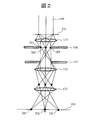
図2を用い、TEM像(透過像)の観察時における電子ビームの軌道を説明する。TEM像の観察時には、照射レンズ102~104(図2中には図示せず)によって、ほぼ平行なビーム130を試料131に照射し、試料131と相互作用した電子を、試料下方に設置された複数段の結像レンズ132、133で拡大する。拡大された像は、CCDカメラ114上で結像し、画像化される。図3は、CCDカメラ114を用いて撮影されたTEM像(透過像)の一例である。
回折パターンを観察する場合には、図2に示すように、試料下方に結像される回折スポット201と透過スポット202を複数段の結像レンズ132、133を用いて拡大する。拡大された回折スポット201と透過スポット202は、CCDカメラ114上で結像し、画像化される。回折パターンを観察する場合に結像レンズ132、133に流す電流値は、TEM像を観察する場合に結像レンズ132、133に流す電流値と異なる。電流値の切り替えは主制御部121が実行する。図4は、TEM像に対応する回折パターンの一例である。CCDカメラ114によって撮影された画像上には試料の結晶方位に応じた回折パターン(回折スポット201、透過スポット202)が観察される。
図2に示すように、回折スポット201が結像される領域の近傍には、対物絞り106が設置されている。対物絞り106は、TEM像(透過像)の観察時には必要のない散乱電子をカットしたり、特定の回折スポット201のみを結像した像(暗視野像)を撮影したりするために用いられる。
以下では、透過型電子顕微鏡を用いてTEM像(透過像)を撮影する場合の動作(実施例1)と回折パターン(回折像)を撮影する場合の動作(実施例2)を別々に説明するが、後述する動作はイオン顕微鏡を含む各種の荷電粒子線装置を用いてTEM像(透過像)や回折パターン(回折像)を撮影する場合にも適用できる。
本実施例では、回折パターンを構成する任意の回折スポットに対応する暗視野像を自動的に取得する観察モードについて説明する。本実施例の観察では、回折パターンと透過像が用いられる。図7に示す回折パターンには透過波と回折波が含まれている。図7中のスポットCが透過波に相当し、それ以外は回折波である。回折波のみを用いて結像させた観察像が暗視野像、透過波のみを用いて結像させた観察像が明視野像である。暗視野像と明視野像を合わせて透過像という。観察像の選択は、対物絞り106により、どの回折スポットを透過させるかの選択により行う。
観察対象である回折パターンのうち任意のスポットに対応する暗視野像を撮影したい場合、作業者は、GUI画面401のモード選択欄402を回折パターン観察モードに切り替える。この選択により、像表示領域400には、回折パターンが表示される。作業者は、表示されている回折パターン上で、暗視野像の撮像を希望する任意の位置の回折スポットを選択する。
回折スポットが指定される度に、主制御装置121は、個々の回折スポットの観察に適した絞り径を有する穴(絞り板150を構成する穴151~154のうちのいずれか)を選択する。ここでの絞り穴の選択は、指定された任意の回折スポットの大きさとほぼ等しい大きさの絞り穴を最適径として選択する場合だけでなく、指定された任意の回折スポットを絞り穴の一部分に含むものを最適径として選択する場合を含む。
主制御装置121は、画面上で選択された全ての回折スポットの座標を計算する。当該座標により、撮影対象とする回折スポットが一意に特定される。この座標は、対物絞りを移動すべき位置を与える。
主制御装置121は、算出された1つ又は複数の回折スポットの座標を不図示のメモリに保存する。すなわち、主制御装置121は、算出された座標をメモリに登録する。以後、主制御装置121は、保存された1つ又は複数の回折スポットの暗視野像を順番に取得する動作モードに移行する。暗視野像の取得は、作業者がTEMボタン404を、ポインティングデバイス180を用いてクリックすることで開始される。
TEMボタン404のクリックを検知した主制御装置121は、まず、回折スポットAの暗視野像の撮影用に対物絞り106の特定の穴(ステップ1102で選択された穴)を、回折スポットAの座標位置に自動的に移動させる。すなわち、回折スポットAと対物絞り106の特定の穴が一致するように、対物絞り106の位置が調整される。
作業者が撮影ボタン405をクリックすると、主制御装置121は、結像レンズの電流値をTEM像観察モードに切り替えて回折スポットAの暗視野像Aを取得し、表示装置123の像表示領域400に表示する。作業者は、この像表示領域400に表示された暗視野像Aを観察する。指定された回折スポットの個数が1つだけの場合には、このステップの処理で終了する。
ステップ1101で複数個の回折スポットが暗視野像の撮影用に登録されている場合、主制御装置121は、他の回折スポットについて順番に暗視野像の撮影処理を自動的に実行する。ここでは、回折スポットBの撮影用に対物絞り106の特定の穴(ステップ1102で選択された穴)を、回折スポットBの座標位置に移動させる。すなわち、回折スポットBと対物絞り106の特定の穴が一致するように、対物絞り106の位置が調整される。このとき、主制御装置121は、観察モードを、回折パターン観察モードに切り替えても良いが、回折スポットBの座標が既に登録されているのでTEM像観察モードのままで良い。
作業者が撮影ボタン405をクリックすると、主制御装置121は、回折スポットBに対応する暗視野像Bを取得し、表示装置123の像表示領域400に表示する。作業者は、この像表示領域400に表示された暗視野像Bを観察する。ステップ1107及び1108の処理は、登録されている全ての回折スポットについて繰り返し実行される。
本実施例では、透過像を構成する部分領域に対応する回折パターンを自動的に取得する観察モードについて説明する。図2に示すように、試料下方の領域部分には、対物レンズで結像された透過像が形成される。この領域部分には制限視野絞り107が取り付けられている。制限視野絞り107は、透過像の特定の領域の回折パターンを取得するために用いられる。制限視野絞り107を構成する絞り板には、図5に示す絞り板150と同様に、複数個の直径0.1μm~数100μm程度の穴が設けられている。結像レンズ110~113に流す電流を制御することにより、試料直下に形成される回折パターンを拡大してCCDカメラ114上に結像するか、対物レンズで結像されたTEM像を拡大してCCDカメラ114上に結像するかを切り替えることができる。
観察対象である透過像のうち任意の範囲に対応する回折パターンを撮影したい場合、作業者は、GUI画面401のモード選択欄402における選択をTEM像観察モードに切り替える。この選択を受信した主制御装置121は、TEM像観察モードに適した電流で結像レンズ110~113を制御する。この結果、像表示領域400にはTEM像が表示される。
作業者は、像表示領域400内に表示されたTEM像のうち任意の範囲を選択する。例えば選択範囲Aを選択する場合、作業者は、GUI画面401に表示されたチェックボックス406のA欄にチェックを入れた後、登録ボタン403をクリックし、更にTEM像のうち観察した任意の範囲Aを指定する。ここでの範囲の指定(選択)は、ポインティングデバイスをクリック又はドラッグするなどして行う。
主制御装置121は、範囲が指定(選択)される度に、その大きさに対応する絞り径を選択する。ここでの絞り径とは、制限視野絞り107を構成する穴の径である。
主制御装置121は、範囲が指定(選択)される度に、その中心座標を計算し、その座標をメモリに保存する。範囲の大きさが任意の場合には、範囲の大きさもメモリに保存される。以後、主制御装置121は、保存された1つ又は複数の範囲に対応する回折パターンを順番に取得する動作モードに移行する。回折パターンの取得は、作業者が回折パターンボタン407を、ポインティングデバイス180を用いてクリックすることで開始される。
主制御装置121は、まず、制限視野絞り107の特定の穴(ステップ1603で選択された穴)を、範囲Aの座標位置に自動的に移動させる。すなわち、構造解析したい範囲と制限視野絞り107の特定の穴が一致するように、制限視野絞り107の位置が調整される。制限視野絞り107の移動は、制限視野絞り107とTEM像との位置関係に応じて定まる。なお、校正時において、制限視野絞り中心と光軸中心とは一致している。両中心が一致することで、カメラ画像の座標系、結像面(一次像面)の座標系、回折面の座標系が相似の関係になり、これらを1つの座標系として扱うことが可能になる。
撮像ボタン405がクリックされると、主制御装置121は、結像レンズの電流値を回折パターン観察モードに切り替えて選択範囲Aに対応する回折パターンAを取得し、表示装置123の像表示領域400に表示する。作業者は、この像表示領域400に表示された回折パターンAを観察する。指定された回折スポットの個数が1つだけの場合には、このステップの処理で終了する。
ステップ1601で複数個の選択範囲が回折パターンの撮影用に登録されている場合、主制御装置121は、他の範囲について順番に回折パターンの撮影処理を自動的に実行する。ここでは、選択範囲Bの撮影用に制限視野絞り107の特定の穴(ステップ1603で選択された穴)を、選択範囲Bの座標位置に移動させる。このとき、主制御装置121は、観察モードを、TEM像観察モードに切り替えても良いが、選択範囲Bの座標が既に登録されているので回折パターン観察モードのままで良い。
撮影ボタン405がクリックされると、主制御装置121は、結像レンズの電流値を回折パターン観察モードに切り替えて選択範囲Bの回折パターンBを取得し、表示装置123の像表示領域400に表示する。作業者は、この像表示領域400に表示された回折パターンBを観察する。ステップ1607及び1608の処理は、登録されている全ての回折スポットについて繰り返し実行される。
なお、本発明は上記した実施例に限定されるものではなく、様々な変形例が含まれる。例えば、上記した実施例は本発明を分かりやすく説明するために詳細に説明したものであり、必ずしも説明した全ての構成を備えるものに限定されるものではない。また、ある実施例の構成の一部を他の実施例の構成に置き換えることも可能であり、また、ある実施例の構成に他の実施例の構成を加えることも可能である。また、各実施例の構成の一部について、他の構成の追加、削除又は置換をすることが可能である。
Claims (8)
- 試料へ荷電粒子線を照射する照射部と、
前記試料の像を結像する結像部と、
前記結像部内に配置され、前記試料からの電子線を通過させるための大きさの異なる複数の開口が形成された絞りと、
前記絞りの位置を変更する移動部と、
前記結像光学系によって結像された像を得る検出部と、
前記検出部で得られた前記像を表示する表示部と、
表示された前記像から所定の部分を選択する選択部と、を有し、
前記移動部は前記所定の部分の選択位置に応じて、前記絞りと前記像との位置関係から前記絞りを移動し、
前記像は、電子線回折像及び前記試料の透過像の少なくとも1つであり、
前記絞りは、前記結像部内の回折面に挿入可能な対物絞り、及び前記結像部内の一次像面に挿入可能な制限視野絞りの少なくとも1つである、荷電粒子線装置。 - 請求項1に記載の荷電粒子線装置において、
前記像は、電子線回折像、及び前記試料の透過像であり、
前記絞りは、前記結像部内の回折面に挿入可能な対物絞り、及び前記結像部内の一次像面に挿入可能な制限視野絞りである、荷電粒子線装置。 - 請求項2に記載の荷電粒子線装置において、
前記絞りの移動距離を計測する計測部と、を有し、
前記移動部は前記計測部の計測結果をフィードバックすることで前記絞りの位置を変更する、荷電粒子線装置。 - 請求項1に記載の荷電粒子線装置において、
前記絞りの移動距離を計測する計測部と、を有し、
前記移動部は前記計測部の計測結果をフィードバックすることで前記絞りの位置を変更する、荷電粒子線装置。 - 試料へ荷電粒子線を照射する照射部と、前記試料の像を結像する結像部と、前記結像部内に配置され、前記試料からの電子線を通過させるための大きさの異なる複数の開口が形成された絞りと、前記絞りの位置を変更する移動部と、前記結像光学系によって結像された像を得る検出部と、前記検出部で得られた前記像を表示する表示部と、表示された前記像から所定の部分を選択する選択部とを有する荷電粒子線装置を用いた試料観察方法において、
前記選択部を通じ、前記表示部に表示された前記像から前記所定の部分の選択を受け付ける処理と、
前記移動部が、前記所定の部分の選択位置に応じて、前記絞りと前記像との位置関係から前記絞りを移動する処理とを有し、
前記像は、電子線回折像及び前記試料の透過像の少なくとも1つであり、
前記絞りは、前記結像部内の回折面に挿入可能な対物絞り、及び、前記結像部内の一次像面に挿入可能な制限視野絞りの少なくとも1つである、前記荷電粒子線装置を用いた試料観察方法。 - 請求項5に記載の荷電粒子線装置を用いた試料観察方法において、
前記像は、電子線回折像及び前記試料の透過像であり、
前記絞りは、前記結像部内の回折面に挿入可能な対物絞り、及び、前記結像部内の一次像面に挿入可能な制限視野絞りである、荷電粒子線装置を用いた試料観察方法。 - 請求項6に記載の荷電粒子線装置を用いた試料観察方法において、
前記移動部は、前記絞りの移動距離を計測する計測部による計測結果をフィードバックすることにより前記絞りの位置を変更する、荷電粒子線装置を用いた試料観察方法。 - 請求項5に記載の荷電粒子線装置を用いた試料観察方法において、
前記移動部は、前記絞りの移動距離を計測する計測部による計測結果をフィードバックすることにより前記絞りの位置を変更する、荷電粒子線装置を用いた試料観察方法。
Priority Applications (5)
| Application Number | Priority Date | Filing Date | Title |
|---|---|---|---|
| CN201580077898.5A CN107408484B (zh) | 2015-04-14 | 2015-04-14 | 带电粒子束装置以及试样观察方法 |
| US15/560,286 US10636621B2 (en) | 2015-04-14 | 2015-04-14 | Charged particle beam device for moving an aperture having plurality of openings and sample observation method |
| JP2017512485A JP6403142B2 (ja) | 2015-04-14 | 2015-04-14 | 荷電粒子線装置及び試料観察方法 |
| PCT/JP2015/061407 WO2016166805A1 (ja) | 2015-04-14 | 2015-04-14 | 荷電粒子線装置及び試料観察方法 |
| DE112015006453.2T DE112015006453B4 (de) | 2015-04-14 | 2015-04-14 | Vorrichtung mit einem Strahl geladener Teilchen und Probenbeobachtungsverfahren |
Applications Claiming Priority (1)
| Application Number | Priority Date | Filing Date | Title |
|---|---|---|---|
| PCT/JP2015/061407 WO2016166805A1 (ja) | 2015-04-14 | 2015-04-14 | 荷電粒子線装置及び試料観察方法 |
Publications (1)
| Publication Number | Publication Date |
|---|---|
| WO2016166805A1 true WO2016166805A1 (ja) | 2016-10-20 |
Family
ID=57126125
Family Applications (1)
| Application Number | Title | Priority Date | Filing Date |
|---|---|---|---|
| PCT/JP2015/061407 Ceased WO2016166805A1 (ja) | 2015-04-14 | 2015-04-14 | 荷電粒子線装置及び試料観察方法 |
Country Status (5)
| Country | Link |
|---|---|
| US (1) | US10636621B2 (ja) |
| JP (1) | JP6403142B2 (ja) |
| CN (1) | CN107408484B (ja) |
| DE (1) | DE112015006453B4 (ja) |
| WO (1) | WO2016166805A1 (ja) |
Cited By (1)
| Publication number | Priority date | Publication date | Assignee | Title |
|---|---|---|---|---|
| US11742176B2 (en) | 2020-11-30 | 2023-08-29 | Jeol Ltd. | Transmission electron microscope and method of adjusting optical system |
Families Citing this family (2)
| Publication number | Priority date | Publication date | Assignee | Title |
|---|---|---|---|---|
| CN111971774B (zh) * | 2018-03-29 | 2023-09-29 | 株式会社日立高新技术 | 带电粒子束装置 |
| PT3779403T (pt) * | 2018-03-29 | 2024-07-10 | Hitachi High Tech Corp | Dispositivo de feixe de partículas carregadas |
Citations (2)
| Publication number | Priority date | Publication date | Assignee | Title |
|---|---|---|---|---|
| JPH04366539A (ja) * | 1991-06-14 | 1992-12-18 | Jeol Ltd | 電子顕微鏡の対物絞り駆動装置 |
| JP2007122998A (ja) * | 2005-10-27 | 2007-05-17 | Jeol Ltd | 荷電粒子ビーム装置及び荷電粒子ビーム装置におけるビーム絞り位置調整方法 |
Family Cites Families (11)
| Publication number | Priority date | Publication date | Assignee | Title |
|---|---|---|---|---|
| JP3148353B2 (ja) * | 1991-05-30 | 2001-03-19 | ケーエルエー・インストルメンツ・コーポレーション | 電子ビーム検査方法とそのシステム |
| JP3112527B2 (ja) | 1991-11-14 | 2000-11-27 | 日本電子株式会社 | 電子顕微鏡 |
| JP3422045B2 (ja) | 1993-06-21 | 2003-06-30 | 株式会社日立製作所 | 組成及び格子歪測定用電子顕微鏡及びその観察方法 |
| JP2001077002A (ja) * | 1999-09-02 | 2001-03-23 | Nikon Corp | 荷電粒子ビーム露光方法、荷電粒子ビーム露光装置及び半導体デバイス製造方法 |
| US7138629B2 (en) * | 2003-04-22 | 2006-11-21 | Ebara Corporation | Testing apparatus using charged particles and device manufacturing method using the testing apparatus |
| JP2007179753A (ja) * | 2005-12-27 | 2007-07-12 | Hitachi High-Technologies Corp | 走査透過電子顕微鏡、及び収差測定方法 |
| JP4994151B2 (ja) | 2007-08-14 | 2012-08-08 | 日本電子株式会社 | 荷電粒子線装置 |
| JP2009110788A (ja) | 2007-10-30 | 2009-05-21 | Jeol Ltd | 透過形電子顕微鏡及びその動作方法 |
| US9123502B2 (en) * | 2009-05-20 | 2015-09-01 | Carl Zeiss Microscopy, Llc | Scan method |
| EP3528276A3 (en) * | 2011-05-13 | 2019-09-04 | Fibics Incorporated | Microscopy imaging method |
| JP2013096900A (ja) * | 2011-11-02 | 2013-05-20 | Jeol Ltd | 透過電子顕微鏡および透過電子顕微鏡像の観察方法 |
-
2015
- 2015-04-14 DE DE112015006453.2T patent/DE112015006453B4/de active Active
- 2015-04-14 WO PCT/JP2015/061407 patent/WO2016166805A1/ja not_active Ceased
- 2015-04-14 CN CN201580077898.5A patent/CN107408484B/zh not_active Expired - Fee Related
- 2015-04-14 JP JP2017512485A patent/JP6403142B2/ja active Active
- 2015-04-14 US US15/560,286 patent/US10636621B2/en active Active
Patent Citations (2)
| Publication number | Priority date | Publication date | Assignee | Title |
|---|---|---|---|---|
| JPH04366539A (ja) * | 1991-06-14 | 1992-12-18 | Jeol Ltd | 電子顕微鏡の対物絞り駆動装置 |
| JP2007122998A (ja) * | 2005-10-27 | 2007-05-17 | Jeol Ltd | 荷電粒子ビーム装置及び荷電粒子ビーム装置におけるビーム絞り位置調整方法 |
Cited By (1)
| Publication number | Priority date | Publication date | Assignee | Title |
|---|---|---|---|---|
| US11742176B2 (en) | 2020-11-30 | 2023-08-29 | Jeol Ltd. | Transmission electron microscope and method of adjusting optical system |
Also Published As
| Publication number | Publication date |
|---|---|
| CN107408484A (zh) | 2017-11-28 |
| JP6403142B2 (ja) | 2018-10-10 |
| US10636621B2 (en) | 2020-04-28 |
| JPWO2016166805A1 (ja) | 2018-02-08 |
| CN107408484B (zh) | 2019-03-15 |
| US20180076004A1 (en) | 2018-03-15 |
| DE112015006453B4 (de) | 2023-02-23 |
| DE112015006453T5 (de) | 2017-12-28 |
Similar Documents
| Publication | Publication Date | Title |
|---|---|---|
| KR101667053B1 (ko) | X 선 분석 장치 및 x 선 분석 방법 | |
| JP4988662B2 (ja) | 荷電粒子線装置 | |
| JP5296413B2 (ja) | 複合荷電粒子ビーム装置を用いた断面画像取得方法および複合荷電粒子ビーム装置 | |
| JP5269521B2 (ja) | X線分析装置及びx線分析方法 | |
| KR102354765B1 (ko) | 형광 x 선 분석 장치 및 그 측정 위치 조정 방법 | |
| JP5315033B2 (ja) | 電子分光器を備えた透過型電子顕微鏡 | |
| DE102013102749A1 (de) | Röntgenstrahl-Messgerät | |
| JP2014026834A (ja) | 荷電粒子線応用装置 | |
| JP2008270056A (ja) | 走査型透過電子顕微鏡 | |
| JP2008210731A (ja) | 電子分光器を備えた透過型電子顕微鏡 | |
| JPH0922676A (ja) | 荷電粒子線装置 | |
| JP6403142B2 (ja) | 荷電粒子線装置及び試料観察方法 | |
| EP2988315A2 (en) | Method for analyzing and/or processing an object as well as a particle beam device for carrying out the method | |
| WO2001040735A1 (fr) | Dispositif d'analyse/observation | |
| JP2016039119A (ja) | 電子顕微鏡、および電子顕微鏡の調整方法 | |
| JP2006173038A (ja) | 荷電粒子線装置、試料像表示方法及びイメージシフト感度計測方法 | |
| WO2009157358A1 (ja) | 電子分光器を有する透過型電子顕微鏡装置,試料ホルダ,試料台及びスペクトル像の取得方法 | |
| JP5397060B2 (ja) | 荷電粒子顕微鏡及び解析方法 | |
| JP3870141B2 (ja) | 電子顕微鏡 | |
| US7173259B2 (en) | Automatically aligning objective aperture for a scanning electron microscope | |
| JP7394535B2 (ja) | 粒子線分析装置 | |
| JP2023054559A (ja) | 画像表示方法、分析システムおよびプログラム | |
| WO2014061690A1 (ja) | 電子顕微鏡 | |
| JP2007266016A (ja) | 電子顕微鏡 | |
| JPH04166753A (ja) | X線分光分析装置 |
Legal Events
| Date | Code | Title | Description |
|---|---|---|---|
| 121 | Ep: the epo has been informed by wipo that ep was designated in this application |
Ref document number: 15889143 Country of ref document: EP Kind code of ref document: A1 |
|
| WWE | Wipo information: entry into national phase |
Ref document number: 15560286 Country of ref document: US |
|
| ENP | Entry into the national phase |
Ref document number: 2017512485 Country of ref document: JP Kind code of ref document: A |
|
| WWE | Wipo information: entry into national phase |
Ref document number: 112015006453 Country of ref document: DE |
|
| 122 | Ep: pct application non-entry in european phase |
Ref document number: 15889143 Country of ref document: EP Kind code of ref document: A1 |