WO2016158588A1 - ワイヤボンディング装置及びワイヤボンディング方法 - Google Patents
ワイヤボンディング装置及びワイヤボンディング方法 Download PDFInfo
- Publication number
- WO2016158588A1 WO2016158588A1 PCT/JP2016/059067 JP2016059067W WO2016158588A1 WO 2016158588 A1 WO2016158588 A1 WO 2016158588A1 JP 2016059067 W JP2016059067 W JP 2016059067W WO 2016158588 A1 WO2016158588 A1 WO 2016158588A1
- Authority
- WO
- WIPO (PCT)
- Prior art keywords
- imaging unit
- wire
- bonding tool
- bonding
- reference member
- Prior art date
- Legal status (The legal status is an assumption and is not a legal conclusion. Google has not performed a legal analysis and makes no representation as to the accuracy of the status listed.)
- Ceased
Links
Images






Classifications
-
- B—PERFORMING OPERATIONS; TRANSPORTING
- B23—MACHINE TOOLS; METAL-WORKING NOT OTHERWISE PROVIDED FOR
- B23K—SOLDERING OR UNSOLDERING; WELDING; CLADDING OR PLATING BY SOLDERING OR WELDING; CUTTING BY APPLYING HEAT LOCALLY, e.g. FLAME CUTTING; WORKING BY LASER BEAM
- B23K1/00—Soldering, e.g. brazing, or unsoldering
- B23K1/06—Soldering, e.g. brazing, or unsoldering making use of vibrations, e.g. supersonic vibrations
-
- H—ELECTRICITY
- H10—SEMICONDUCTOR DEVICES; ELECTRIC SOLID-STATE DEVICES NOT OTHERWISE PROVIDED FOR
- H10W—GENERIC PACKAGES, INTERCONNECTIONS, CONNECTORS OR OTHER CONSTRUCTIONAL DETAILS OF DEVICES COVERED BY CLASS H10
- H10W72/00—Interconnections or connectors in packages
- H10W72/50—Bond wires
-
- B—PERFORMING OPERATIONS; TRANSPORTING
- B23—MACHINE TOOLS; METAL-WORKING NOT OTHERWISE PROVIDED FOR
- B23K—SOLDERING OR UNSOLDERING; WELDING; CLADDING OR PLATING BY SOLDERING OR WELDING; CUTTING BY APPLYING HEAT LOCALLY, e.g. FLAME CUTTING; WORKING BY LASER BEAM
- B23K20/00—Non-electric welding by applying impact or other pressure, with or without the application of heat, e.g. cladding or plating
- B23K20/002—Non-electric welding by applying impact or other pressure, with or without the application of heat, e.g. cladding or plating specially adapted for particular articles or work
- B23K20/004—Wire welding
- B23K20/005—Capillary welding
- B23K20/007—Ball bonding
-
- B—PERFORMING OPERATIONS; TRANSPORTING
- B23—MACHINE TOOLS; METAL-WORKING NOT OTHERWISE PROVIDED FOR
- B23K—SOLDERING OR UNSOLDERING; WELDING; CLADDING OR PLATING BY SOLDERING OR WELDING; CUTTING BY APPLYING HEAT LOCALLY, e.g. FLAME CUTTING; WORKING BY LASER BEAM
- B23K20/00—Non-electric welding by applying impact or other pressure, with or without the application of heat, e.g. cladding or plating
- B23K20/26—Auxiliary equipment
-
- B—PERFORMING OPERATIONS; TRANSPORTING
- B23—MACHINE TOOLS; METAL-WORKING NOT OTHERWISE PROVIDED FOR
- B23K—SOLDERING OR UNSOLDERING; WELDING; CLADDING OR PLATING BY SOLDERING OR WELDING; CUTTING BY APPLYING HEAT LOCALLY, e.g. FLAME CUTTING; WORKING BY LASER BEAM
- B23K3/00—Tools, devices or special appurtenances for soldering, e.g. brazing, or unsoldering, not specially adapted for particular methods
- B23K3/08—Auxiliary devices therefor
-
- B—PERFORMING OPERATIONS; TRANSPORTING
- B23—MACHINE TOOLS; METAL-WORKING NOT OTHERWISE PROVIDED FOR
- B23K—SOLDERING OR UNSOLDERING; WELDING; CLADDING OR PLATING BY SOLDERING OR WELDING; CUTTING BY APPLYING HEAT LOCALLY, e.g. FLAME CUTTING; WORKING BY LASER BEAM
- B23K35/00—Rods, electrodes, materials, or media, for use in soldering, welding, or cutting
- B23K35/02—Rods, electrodes, materials, or media, for use in soldering, welding, or cutting characterised by mechanical features, e.g. shape
- B23K35/0255—Rods, electrodes, materials, or media, for use in soldering, welding, or cutting characterised by mechanical features, e.g. shape for use in welding
- B23K35/0261—Rods, electrodes or wires
-
- H—ELECTRICITY
- H10—SEMICONDUCTOR DEVICES; ELECTRIC SOLID-STATE DEVICES NOT OTHERWISE PROVIDED FOR
- H10W—GENERIC PACKAGES, INTERCONNECTIONS, CONNECTORS OR OTHER CONSTRUCTIONAL DETAILS OF DEVICES COVERED BY CLASS H10
- H10W72/00—Interconnections or connectors in packages
- H10W72/01—Manufacture or treatment
- H10W72/015—Manufacture or treatment of bond wires
-
- H—ELECTRICITY
- H10—SEMICONDUCTOR DEVICES; ELECTRIC SOLID-STATE DEVICES NOT OTHERWISE PROVIDED FOR
- H10W—GENERIC PACKAGES, INTERCONNECTIONS, CONNECTORS OR OTHER CONSTRUCTIONAL DETAILS OF DEVICES COVERED BY CLASS H10
- H10W72/00—Interconnections or connectors in packages
- H10W72/071—Connecting or disconnecting
- H10W72/0711—Apparatus therefor
-
- H—ELECTRICITY
- H10—SEMICONDUCTOR DEVICES; ELECTRIC SOLID-STATE DEVICES NOT OTHERWISE PROVIDED FOR
- H10W—GENERIC PACKAGES, INTERCONNECTIONS, CONNECTORS OR OTHER CONSTRUCTIONAL DETAILS OF DEVICES COVERED BY CLASS H10
- H10W72/00—Interconnections or connectors in packages
- H10W72/071—Connecting or disconnecting
- H10W72/075—Connecting or disconnecting of bond wires
-
- B—PERFORMING OPERATIONS; TRANSPORTING
- B23—MACHINE TOOLS; METAL-WORKING NOT OTHERWISE PROVIDED FOR
- B23K—SOLDERING OR UNSOLDERING; WELDING; CLADDING OR PLATING BY SOLDERING OR WELDING; CUTTING BY APPLYING HEAT LOCALLY, e.g. FLAME CUTTING; WORKING BY LASER BEAM
- B23K2101/00—Articles made by soldering, welding or cutting
- B23K2101/36—Electric or electronic devices
- B23K2101/40—Semiconductor devices
-
- B—PERFORMING OPERATIONS; TRANSPORTING
- B23—MACHINE TOOLS; METAL-WORKING NOT OTHERWISE PROVIDED FOR
- B23K—SOLDERING OR UNSOLDERING; WELDING; CLADDING OR PLATING BY SOLDERING OR WELDING; CUTTING BY APPLYING HEAT LOCALLY, e.g. FLAME CUTTING; WORKING BY LASER BEAM
- B23K2101/00—Articles made by soldering, welding or cutting
- B23K2101/36—Electric or electronic devices
- B23K2101/42—Printed circuits
-
- H—ELECTRICITY
- H10—SEMICONDUCTOR DEVICES; ELECTRIC SOLID-STATE DEVICES NOT OTHERWISE PROVIDED FOR
- H10W—GENERIC PACKAGES, INTERCONNECTIONS, CONNECTORS OR OTHER CONSTRUCTIONAL DETAILS OF DEVICES COVERED BY CLASS H10
- H10W72/00—Interconnections or connectors in packages
- H10W72/01—Manufacture or treatment
- H10W72/015—Manufacture or treatment of bond wires
- H10W72/01551—Changing the shapes of bond wires
-
- H—ELECTRICITY
- H10—SEMICONDUCTOR DEVICES; ELECTRIC SOLID-STATE DEVICES NOT OTHERWISE PROVIDED FOR
- H10W—GENERIC PACKAGES, INTERCONNECTIONS, CONNECTORS OR OTHER CONSTRUCTIONAL DETAILS OF DEVICES COVERED BY CLASS H10
- H10W72/00—Interconnections or connectors in packages
- H10W72/071—Connecting or disconnecting
- H10W72/0711—Apparatus therefor
- H10W72/07141—Means for applying energy, e.g. ovens or lasers
-
- H—ELECTRICITY
- H10—SEMICONDUCTOR DEVICES; ELECTRIC SOLID-STATE DEVICES NOT OTHERWISE PROVIDED FOR
- H10W—GENERIC PACKAGES, INTERCONNECTIONS, CONNECTORS OR OTHER CONSTRUCTIONAL DETAILS OF DEVICES COVERED BY CLASS H10
- H10W72/00—Interconnections or connectors in packages
- H10W72/071—Connecting or disconnecting
- H10W72/0711—Apparatus therefor
- H10W72/07168—Means for storing or moving the material for the connector
-
- H—ELECTRICITY
- H10—SEMICONDUCTOR DEVICES; ELECTRIC SOLID-STATE DEVICES NOT OTHERWISE PROVIDED FOR
- H10W—GENERIC PACKAGES, INTERCONNECTIONS, CONNECTORS OR OTHER CONSTRUCTIONAL DETAILS OF DEVICES COVERED BY CLASS H10
- H10W72/00—Interconnections or connectors in packages
- H10W72/071—Connecting or disconnecting
- H10W72/0711—Apparatus therefor
- H10W72/07178—Means for aligning
-
- H—ELECTRICITY
- H10—SEMICONDUCTOR DEVICES; ELECTRIC SOLID-STATE DEVICES NOT OTHERWISE PROVIDED FOR
- H10W—GENERIC PACKAGES, INTERCONNECTIONS, CONNECTORS OR OTHER CONSTRUCTIONAL DETAILS OF DEVICES COVERED BY CLASS H10
- H10W72/00—Interconnections or connectors in packages
- H10W72/071—Connecting or disconnecting
- H10W72/0711—Apparatus therefor
- H10W72/07183—Means for monitoring
-
- H—ELECTRICITY
- H10—SEMICONDUCTOR DEVICES; ELECTRIC SOLID-STATE DEVICES NOT OTHERWISE PROVIDED FOR
- H10W—GENERIC PACKAGES, INTERCONNECTIONS, CONNECTORS OR OTHER CONSTRUCTIONAL DETAILS OF DEVICES COVERED BY CLASS H10
- H10W72/00—Interconnections or connectors in packages
- H10W72/071—Connecting or disconnecting
- H10W72/075—Connecting or disconnecting of bond wires
- H10W72/07511—Treating the bonding area before connecting, e.g. by applying flux or cleaning
-
- H—ELECTRICITY
- H10—SEMICONDUCTOR DEVICES; ELECTRIC SOLID-STATE DEVICES NOT OTHERWISE PROVIDED FOR
- H10W—GENERIC PACKAGES, INTERCONNECTIONS, CONNECTORS OR OTHER CONSTRUCTIONAL DETAILS OF DEVICES COVERED BY CLASS H10
- H10W72/00—Interconnections or connectors in packages
- H10W72/071—Connecting or disconnecting
- H10W72/075—Connecting or disconnecting of bond wires
- H10W72/07521—Aligning
- H10W72/07523—Active alignment, e.g. using optical alignment using marks or sensors
-
- H—ELECTRICITY
- H10—SEMICONDUCTOR DEVICES; ELECTRIC SOLID-STATE DEVICES NOT OTHERWISE PROVIDED FOR
- H10W—GENERIC PACKAGES, INTERCONNECTIONS, CONNECTORS OR OTHER CONSTRUCTIONAL DETAILS OF DEVICES COVERED BY CLASS H10
- H10W72/00—Interconnections or connectors in packages
- H10W72/071—Connecting or disconnecting
- H10W72/075—Connecting or disconnecting of bond wires
- H10W72/07531—Techniques
-
- H—ELECTRICITY
- H10—SEMICONDUCTOR DEVICES; ELECTRIC SOLID-STATE DEVICES NOT OTHERWISE PROVIDED FOR
- H10W—GENERIC PACKAGES, INTERCONNECTIONS, CONNECTORS OR OTHER CONSTRUCTIONAL DETAILS OF DEVICES COVERED BY CLASS H10
- H10W72/00—Interconnections or connectors in packages
- H10W72/50—Bond wires
- H10W72/551—Materials of bond wires
- H10W72/552—Materials of bond wires comprising metals or metalloids, e.g. silver
-
- H—ELECTRICITY
- H10—SEMICONDUCTOR DEVICES; ELECTRIC SOLID-STATE DEVICES NOT OTHERWISE PROVIDED FOR
- H10W—GENERIC PACKAGES, INTERCONNECTIONS, CONNECTORS OR OTHER CONSTRUCTIONAL DETAILS OF DEVICES COVERED BY CLASS H10
- H10W72/00—Interconnections or connectors in packages
- H10W72/50—Bond wires
- H10W72/551—Materials of bond wires
- H10W72/552—Materials of bond wires comprising metals or metalloids, e.g. silver
- H10W72/5522—Materials of bond wires comprising metals or metalloids, e.g. silver comprising gold [Au]
-
- H—ELECTRICITY
- H10—SEMICONDUCTOR DEVICES; ELECTRIC SOLID-STATE DEVICES NOT OTHERWISE PROVIDED FOR
- H10W—GENERIC PACKAGES, INTERCONNECTIONS, CONNECTORS OR OTHER CONSTRUCTIONAL DETAILS OF DEVICES COVERED BY CLASS H10
- H10W72/00—Interconnections or connectors in packages
- H10W72/50—Bond wires
- H10W72/551—Materials of bond wires
- H10W72/552—Materials of bond wires comprising metals or metalloids, e.g. silver
- H10W72/5525—Materials of bond wires comprising metals or metalloids, e.g. silver comprising copper [Cu]
-
- H—ELECTRICITY
- H10—SEMICONDUCTOR DEVICES; ELECTRIC SOLID-STATE DEVICES NOT OTHERWISE PROVIDED FOR
- H10W—GENERIC PACKAGES, INTERCONNECTIONS, CONNECTORS OR OTHER CONSTRUCTIONAL DETAILS OF DEVICES COVERED BY CLASS H10
- H10W90/00—Package configurations
- H10W90/701—Package configurations characterised by the relative positions of pads or connectors relative to package parts
- H10W90/751—Package configurations characterised by the relative positions of pads or connectors relative to package parts of bond wires
- H10W90/754—Package configurations characterised by the relative positions of pads or connectors relative to package parts of bond wires between a chip and a stacked insulating package substrate, interposer or RDL
Definitions
- the present invention relates to a wire bonding apparatus and a wire bonding method.
- this offset is a very important parameter. This offset is radiant heat from the bonding stage and heat generation in the surrounding optical system. In the wire bonding, it is required to accurately grasp such a change in the offset because it changes with time due to wear or the like by the moving mechanism for the bonding process.
- the outer diameter axis center (center) of the bonding tool and the inner hole axis center (center) are not necessarily aligned and are eccentric, or formed at the tip of the bonding tool. Since the free air ball (FAB) itself may be eccentric from the center (center) of the bonding tool, it may not be possible to accurately measure the offset even if the outer diameter axis (center) of the bonding tool is used as a reference. . *
- Patent Document 1 various configurations for measuring the change in the offset are known (for example, Patent Document 1).
- the camera is set at the height of the imaging target such as a reference. It is not always possible to simplify the mechanism and method for measurement.
- an aspect in which wire bonding is performed on a semiconductor chip having a stack structure is increasing, and it is desired to measure an offset easily and accurately in such an aspect.
- the present invention has been made in view of such circumstances, and provides a wire bonding apparatus and a wire bonding method capable of easily and accurately measuring an offset for wire bonding and improving the accuracy of wire bonding. For the purpose.
- a wire bonding apparatus includes a first imaging unit that detects a position of a bonding target on a reference plane, a bonding tool that is provided apart from the first imaging unit, a bonding tool, and a first imaging unit.
- a moving mechanism that integrally moves the unit in a direction parallel to the reference plane, a reference member, a second imaging unit disposed on the opposite side of the reference plane from the bonding tool and the first imaging unit, and a bonding tool
- the position of the optical axis of the first imaging unit with respect to the position of the member is detected, and the second imaging unit moves the bonding tool above the reference member according to the offset value stored in advance.
- the control unit detects the position of the bonding tool based on each detection result by the first imaging unit and the second imaging unit. A change in offset with respect to the first imaging unit is measured.
- the position of the reference member is detected by the second imaging unit disposed on the opposite side of the reference surface S from the bonding tool and the first imaging unit, and the position of the ball-shaped tip of the wire is also detected. Is detected. Since the position of the ball tip is detected by the second image pickup unit, the position detection is not hindered by, for example, foreign matter adhering to the bonding tool, and the accuracy is deteriorated due to deformation of the bonding tool which is a consumable item. In addition, the position of the bonding tool in the XY-axis direction can be detected with few steps. Further, the position of the ball-shaped tip with respect to the position of the reference member can be measured more easily (for example, simultaneously with one detection) by the second imaging unit. Therefore, the offset for wire bonding can be measured easily and accurately. *
- the reference member may include a first mark detected by the first imaging unit and a second mark detected by the second imaging unit.
- the first mark may be a tapered surface of the reference member.
- the first mark may be a step of the reference member.
- the reference member may have an opening bottom portion surrounded by a tapered surface or a step, and the second mark may be formed on the opening bottom portion.
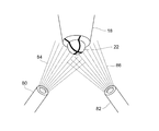
- the wire bonding apparatus further includes an irradiation unit that irradiates the ball-shaped tip portion of the wire from the opposite side of the bonding tool with each slit light in the XY-axis direction parallel to the reference plane, and the control unit is configured in the XY-axis direction. Based on each of the slit lights, an offset change between the bonding tool and the first imaging unit may be measured.
- control unit may measure at least one of a diameter and a shape of a ball-shaped tip portion of the wire extending from the bonding tool.
- the reference member may include an optical path length correction unit
- the second imaging unit may detect the position of the ball-shaped tip of the wire via the optical path length correction unit of the reference member.
- control unit may feed back the measured change in offset and reflect it in the next wire bonding.
- the offset value stored in advance may be an offset value previously measured by the control unit.
- control unit may measure the oxidation level of the ball-shaped tip of the wire based on the detection result of the second imaging unit.
- control unit may feed back to a bonding parameter and reflect it in the next wire bonding.
- the second imaging unit may detect a change accompanying the movement of the ball-shaped tip of the wire when the bonding tool is moved in a direction perpendicular to the reference plane.
- a wire bonding method is a method of wire bonding a position to be bonded on a reference surface, which is a step of preparing a wire bonding apparatus, and is provided apart from a first imaging unit.
- a bonding tool, a moving mechanism for integrally moving the bonding tool and the first imaging unit in a direction parallel to the reference plane, a reference member, and the bonding tool and the first imaging unit opposite to the reference plane A step of preparing a wire bonding apparatus including a second imaging unit disposed and a control unit for measuring an offset between the bonding tool and the first imaging unit; and a wire extending from the bonding tool in a ball shape
- the step of forming the tip, and the first imaging unit is moved above the reference member, and then the reference is performed by the first imaging unit.
- the position of the reference member is detected by the second imaging unit disposed on the opposite side of the reference surface S from the bonding tool and the first imaging unit, and the position of the ball-shaped tip of the wire is also detected. Is detected. Since the position of the ball tip is detected by the second image pickup unit, the position detection is not hindered by, for example, foreign matter adhering to the bonding tool, and the accuracy is deteriorated due to deformation of the bonding tool which is a consumable item. In addition, the position of the bonding tool in the XY-axis direction can be detected with few steps. Further, the position of the ball-shaped tip with respect to the position of the reference member can be measured more easily (for example, simultaneously with one detection) by the second imaging unit. Therefore, the offset for wire bonding can be measured easily and accurately.
- the offset for wire bonding can be measured easily and accurately, and the accuracy of wire bonding can be improved.
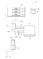
- FIG. 1 is a diagram showing a wire bonding apparatus according to an embodiment of the present invention.
- FIG. 2 is a view showing a wire bonding apparatus according to an embodiment of the present invention.
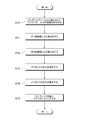
- FIG. 3 is a flowchart illustrating a wire bonding method according to an embodiment of the present invention.
- FIG. 4 is a diagram illustrating a wire bonding method according to an embodiment of the present invention.
- FIG. 5 is a diagram illustrating a wire bonding method according to an embodiment of the present invention.
- FIG. 6 is a diagram illustrating a wire bonding method according to an embodiment of the present invention.
- FIG. 7 is a diagram illustrating a wire bonding method according to an embodiment of the present invention.
- FIG. 8 is a diagram for explaining a wire bonding method according to an embodiment of the present invention.
- FIGS. 9A and 9B are diagrams illustrating a wire bonding method according to an embodiment of the present invention.
- FIG. 10 is a diagram illustrating a wire bonding method according to an embodiment of the present invention.
- FIG. 11 is a diagram illustrating a wire bonding method according to an embodiment of the present invention.
- FIG. 12 is a diagram showing a modification of the embodiment of the present invention.
- FIG. 13 is a diagram showing a modification of the embodiment of the present invention.
- FIGS. 14A and 14B are diagrams showing a modification of the embodiment of the present invention.
- FIG. 15 is a diagram showing a modification of the embodiment of the present invention.
- FIG. 1 and 2 show a wire bonding apparatus 10 according to the present embodiment.
- FIG. 1 is a view seen from the Y-axis direction
- FIG. 2 is a view seen from the X-axis direction. *
- the wire bonding apparatus 10 includes an XY table 12, a bonding head 14, a bonding arm 16, a bonding tool 18, a first imaging unit 30, a second imaging unit 40, and a control unit 60 that performs processing necessary for wire bonding.
- the XY axis direction is a direction parallel to the reference plane S
- the Z axis direction is a direction perpendicular to the reference plane S.
- the wire bonding apparatus 10 is an apparatus for performing a wire bonding method on the bonding target 100 on the reference surface S.
- a first bonding point for example, an electrode of a semiconductor chip
- a second bonding point for example, an electrode of a circuit board
- the bonding target 100 is placed on a bonding stage (not shown) on the reference surface S, and is configured to be able to move the bonding target 100 in the X-axis direction by a transport driving mechanism such as a guide rail.
- the bonding stage is provided with a heating mechanism (not shown), and other components of the wire bonding apparatus 10 receive radiant heat by the heating mechanism of the bonding stage. *
- the bonding target 100 may include, for example, a stack structure in which two or more semiconductor chips are stacked with their electrode pads exposed.
- the wire bonding apparatus and the wire bonding method according to the present embodiment can perform wire bonding accurately with an easy and simple configuration even when the heights of bond points for wire bonding are different, such as a stack structure. it can. *
- the XY table 12 is an example of a moving mechanism.
- the XY table 12 is configured to be slidable in the XY axis direction, and a bonding head 14 is mounted on the XY table.
- the bonding head 14 is provided with a bonding arm 16 via a Z-axis drive mechanism (not shown) that can swing in the Z-axis direction, and a bonding tool 18 is attached to the tip of the bonding arm 16.
- the bonding head 14 is provided with a first imaging unit 30 via a holder 15.
- the bonding tool 18 is configured to insert the wire 20 along the Z-axis direction.
- the bonding tool 18 is, for example, a capillary.
- the bonding arm 16 is provided with a transducer and an ultrasonic transducer (not shown) so that ultrasonic vibration can be applied to the bonding object 100 via the bonding tool 18.
- the bonding tool 18 has an insertion hole for inserting the wire 20 along the Z-axis direction.
- a wire clamper 19 is provided above the bonding tool 18, and the wire clamper 19 is configured to restrain or release the wire 20 at a predetermined timing.
- a ball-shaped tip 22 may be formed at the tip (the lower end in the Z-axis direction) of the wire 20 inserted through the bonding tool 18.
- the material of the wire 20 is appropriately selected from the cost, low electrical resistance, and the like.
- a metal material such as gold (Au), copper (Cu), or silver (Ag) is used.
- the ball-shaped tip 22 is called a free air ball (FAB), and this portion is bonded to the first bond point of the bonding target 100.
- FAB free air ball
- the axis 18a serving as a reference for alignment of the bonding tool 18 may be the axis of the ball-shaped tip 22 in the Z-axis direction, or may be the axis of the insertion hole of the bonding tool 18. . *
- the first imaging unit 30 is for detecting the position of the bonding target 100 on the reference plane S, and is, for example, a photoelectric conversion type camera using a CCD (Charge CoupledCCDDevice).
- the first imaging unit 30 has an optical axis 30a along the Z-axis direction.
- the first imaging unit 30 is arranged on the upper side in the Z-axis direction (that is, the same side as the bonding tool 18) with respect to the reference plane S, and is a predetermined range of the reference plane S from the upper side in the Z-axis direction. Is acquired as image information. *
- the bonding tool 18 and the first imaging unit 30 are provided apart from each other. Specifically, the axis 18a of the bonding tool 18 and the optical axis 30a of the first imaging unit 30 are provided at positions separated by a distance Xt in the X-axis direction and a distance Yt in the Y-axis direction, respectively. .
- the distances Xt and Yt are called offsets. Details of the offset will be described later. *
- the second imaging unit 40 is disposed on the lower side in the Z-axis direction with respect to the reference plane S (that is, on the opposite side of the bonding tool 18 and the first imaging unit 30 with respect to the reference plane S), and the Z-axis A predetermined range of the reference plane S is acquired as image information from the lower side of the direction.
- the second imaging unit 40 is a camera similar to the first imaging unit 30, for example.
- the second imaging unit 40 has an optical axis 40 a along the Z-axis direction, and an illumination 42, a lens 44 (for example, a telecentric lens), and a reference member 50 along the optical axis 40 a. Is provided.
- These reference members 50 and the like provided in the second imaging unit 40 are integrally formed and move together with the second imaging unit 40. Details of the reference member 50 will be described later. *
- the control unit 60 is connected to the components of the wire bonding apparatus 10 such as the XY table 12, the first imaging unit 30, and the second imaging unit 40 so that signals can be transmitted and received. To control. In the present embodiment, the control unit 60 acquires each of the drive unit 62 that controls the movement of the XY table 12, the bonding tool 18, and the first imaging unit 30, and the first and second imaging units 30 and 40. A storage unit 64 that stores image information and the like, and a measurement unit 66 that measures an offset based on each image information stored in the storage unit 64 are provided. Each configuration of the control unit 60 will be described in detail in a wire bonding method described later. *
- control unit 60 is a computer device including a CPU and a memory, and the memory stores in advance a bonding program for performing processing necessary for wire bonding and other necessary information.
- the control unit 60 is configured to perform each process for performing wire bonding described in a wire bonding method to be described later (for example, a program for causing a computer to execute each process).
- FIG. 3 is a flowchart showing the wire bonding method according to the present embodiment.
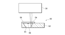
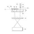
- 4 to 7 are diagrams for explaining each process of the wire bonding method according to the present embodiment. Specifically, FIGS. 4 and 5 show a detection process by the first imaging unit. 6 and 7 show a detection process by the second imaging unit. *
- a ball-shaped tip 22 is formed in a portion extending from the bonding tool 18 in the wire 20 inserted through the bonding tool 18 (S10).
- the step of forming the ball-shaped tip 22 is performed by bringing the tip of the wire 20 extending from the lower end in the vertical direction of the bonding tool 18 close to a torch electrode (not shown) applied with a predetermined high voltage. This is performed by generating a discharge and melting the tip of the wire heated thereby.
- detection by the first imaging unit 30 is performed (S11). Specifically, the drive unit 62 moves the XY table 12 to place the first imaging unit 30 above the reference member 50, and the first imaging unit 30 uses the light of the first imaging unit 30 relative to the position of the reference member 50. The position of the shaft 30a is detected. Data detected by the first imaging unit 30 is stored in the storage unit 64. *
- the reference member 50 has at least one mark (identification unit) that can be detected by the first imaging unit 30 and the second imaging unit 40.
- the reference member 50 is made of a light transmissive material such as glass.
- the reference member 50 includes a base 52 and a cover 56, and the base 52 is an example of an optical path length correction unit.
- the base 52 and the cover 56 are formed in a substantially plate shape.
- An opening hole is formed in the base 52, and a tapered surface 54 inclined with respect to the Z-axis direction is formed inside the opening hole, and this tapered surface 54 becomes a first mark detected by the first imaging unit 30. .
- a metal film 58 is formed on the cover 56 by, for example, vapor deposition or sputtering, and this metal film 58 becomes a second mark detected by the second imaging unit 40. Since the metal film 58 that is the second mark is formed on the lower surface side of the cover 56, adhesion of foreign matter or the like to the metal film 58 is prevented.
- a metal film 58 that is a second mark is formed on the bottom of the opening (cover 56) surrounded by the tapered surface 54 that is the first mark of the reference member 50.
- one mark formed on the reference member 50 may be used for detection of both the first imaging unit 30 and the second imaging unit 40.
- the configurations of the first and second marks are not limited to the above modes as long as they can be detected by the corresponding imaging units.
- the second mark is not limited to the metal film, and may be a marking line or paint drawn on the base 52, or a hole.
- the reference member 50 is not limited to being configured as a separate body of the base 52 and the cover 56, and both may be integrally formed. *
- the position of the tapered surface 54 of the reference member 50 is detected by the first imaging unit 30. Since the tapered surface 54 is inclined with respect to the optical axis in the Z-axis direction of the first imaging unit 30, even if the focus position in the Z-axis direction of the first imaging unit 30 is changed, the first imaging unit 30. Thus, the position of the reference member 50 can be detected. In particular, in the semiconductor device having a stack structure, it is effective to apply the present embodiment because the focus position in the Z-axis direction in the first imaging unit 30 is frequently changed. *
- the position of the optical axis 30a of the first imaging unit 30 with respect to the position of the reference member 50 is detected.
- the first imaging unit 30 may align the optical axis 30a with the center of the ring of the tapered surface 54 of the reference member 50, but it is sufficient if the relative position of both can be detected.
- the optical axis 30 a of the first imaging unit 30 may be moved to a position that does not coincide with the center of the ring of the tapered surface 54.
- the distances ⁇ X1 and ⁇ Y1 between the optical axis 30a of the first imaging unit 30 and the center of the ring of the tapered surface 54 are measured.
- the axis 18a of the bonding tool 18 is located outside the field of view of the first imaging unit 30 that is offset from the optical axis 30a of the first imaging unit 30 by the distances Xt and Yt.
- detection by the second imaging unit 40 is performed (S12). Specifically, first, by driving the XY table 12 by the drive unit 62, the axis 18a of the bonding tool 18 is moved in the direction of the reference member 50 by predetermined distances Xw and Yw. As shown, the bonding tool 18 is disposed above the reference member 50 so that the axial center 18a of the bonding tool 18 falls within the field of view of the second imaging unit 40.
- the distances Xw and Yw are previously stored in the storage unit 64 before the detection step (S12) by the second imaging unit 40, and specifically, the wire bonding apparatus 10 is turned on.
- the bonding tool 18 and the first imaging unit 3 If the offset from 0 has not changed over time and remains the same as the previous measurement offset, when the bonding tool 18 is moved in the direction of the reference member 50, the axis 18 a of the bonding tool 18 is moved to the bonding tool 18. This coincides with the optical axis 30a of the first imaging unit 30 before the movement. However, in reality, the offset changes over time due to various factors associated with continuing the wire bonding process, so the two do not coincide with each other and are offset from each other. Will be brought.
- FIG. 6 shows a detection mode by the second imaging unit 40.
- the bonding tool 18 is lowered above the reference member 50 along the Z-axis direction, the position of the metal film 58 as the second mark of the reference member 50 and the bonding tool are set by the second imaging unit 40.
- the position of the ball-shaped tip 22 which is the 18 axis 18a is detected. That is, the position of the axis 18 a of the bonding tool 18 relative to the position of the reference member 50 is detected by the second imaging unit 40.
- Data detected by the second imaging unit 40 is stored in the storage unit 64. *
- the second imaging unit 40 is configured so that the focus position is in alignment with at least one of the metal film 58 of the reference member 50 and the ball-shaped tip 22 that is the axis of the bonding tool 18.
- the height Z2 of the ball-shaped tip 22 of the bonding tool 18 is disposed above the height Z1 of the metal film 58 of the reference member 50 in the Z-axis direction away from the second imaging unit 40, both When the optical path for detecting the light passes through the same medium, if the focus position is adjusted to one, the other is shifted.
- the position of the ball-shaped tip portion 22 of the bonding tool 18 is detected via the base 52 that is the optical path length correction portion of the reference member 50, thereby causing a focus position shift due to a difference in height.
- Correct For example, as shown in FIG. 6, the optical path from the second imaging unit 40 to the metal film 58 passes through the atmosphere, while the optical path from the second imaging unit 40 to the ball-shaped tip 22 is a glass (thickness a1).
- the focus position deviation amount ⁇ becomes ⁇ a (1-1 / n), and the height can be adjusted by appropriately adjusting the focus deviation amount.
- the deviation can be corrected and the position of the axis 18a of the bonding tool 18 with respect to the position of the reference member 50 can be detected simultaneously. In this way, as shown in FIG. 7, the distances ⁇ X2 and ⁇ Y2 between the axis 18a of the bonding tool 18 and the metal film 58 as the second mark of the reference member 50 are measured. *
- the measuring unit 66 causes an offset between the axis 18a of the bonding tool 18 and the optical axis 30a of the first imaging unit 30. Is measured (S13).
- the change in offset ( ⁇ X and ⁇ Y) has the following relationship with the offset (Xw and Yw) of the previous measurement stored in the storage unit 64 and the actual offset (Xt and Yt). . *
- ⁇ X and ⁇ Y have the following relationship with the measurement by the first imaging unit 30 ( ⁇ X1 and ⁇ Y1) and the measurement by the second imaging unit 40 ( ⁇ X2 and ⁇ Y2). *
- ⁇ X ⁇ X1- ⁇ X2
- ⁇ Y ⁇ Y1- ⁇ Y2
- the offset change is corrected (S14). Specifically, the previously measured offset data stored in the storage unit 64 is corrected to actual offset data in consideration of the change in the offset. In this way, the offset between the bonding tool 18 and the first imaging unit 30 can be measured and corrected accurately and easily. Then, the measured change in the offset is fed back, and wire bonding is performed on the bonding target 100 based on the accurate offset value (S15). Note that such a series of offset measurement and correction processes are repeatedly performed in a fixed cycle in the wire bonding process, and can appropriately cope with a change with time in offset that may occur during the manufacturing process. *
- the second imaging portion 40 measures the offset change in the offset change measuring step (S13).
- the irradiation units 80 and 82 may be integrally movable with respect to the second imaging unit 40 or may be fixed.
- the irradiation units 80 and 82 irradiate the slit light beams 84 and 86 toward the ball-shaped tip 22 of the bonding tool 18 after moving by the distances Xw and Yw which are the offsets of the previous measurement.
- the outer shape of the bonding tool 18 and the ball-like tip 22 FAB
- the change point of the slit light on the ball-shaped tip 22 can be detected by image processing by the light cutting method.
- the relative position of the center of the ball-shaped tip 22 with respect to the outer shape of the bonding tool 18 can be grasped, and the change in offset can be measured more easily and accurately.
- the intersection of the X-axis direction slit light 84a and the Y-axis direction slit light 86a is the ball tip. This coincides with the axis of the portion 22 (or the end surface on the lower end side of the bonding tool 18) in the Z-axis direction.
- the intersection of the X-axis direction slit light 84b and the Y-axis direction slit light 86b is the ball-shaped tip.
- the portion 22 (or the end surface on the lower end portion side of the bonding tool 18) is disposed so as not to coincide with the axis in the Z-axis direction.
- the second imaging unit 40 can recognize the outer edge of the end surface on the lower end side of the bonding tool 18 and the changing point of each slit due to the outer edge of the ball-shaped tip 22, thereby The positions of the axis (Xa, Ya) of the tip 22 and the axis (Xb, Yb) of the bonding tool 18 can be detected. Thereby, the change of the offset can be measured more easily and accurately.
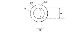
- the axis 18a of the bonding tool 18 is moved to an accurate position (that is, moved by ⁇ X and ⁇ Y), and then the slit light is further applied to the ball-shaped tip 22 of the bonding tool 18.
- 84c and 86c may be irradiated, and the diameter and shape of the ball-shaped tip 22 may be measured by the second imaging unit 40 based on each slit light.
- the distance A between the changing points of the slit light 86c by the outer edge of the ball-shaped tip 22 may be measured, and thereby the diameter of the ball-shaped tip 22 may be detected.
- the distance B to the top of the spherical surface of the ball-shaped tip 22 may be measured, and thereby the shape (that is, the degree of deformation) of the ball-shaped tip 22 may be detected.
- the measuring unit 66 can measure the oxidation level of the ball-shaped tip portion 22.
- the ball-shaped tip 22 may be oxidized, and when the ball-shaped tip 22 is oxidized, the color of the wire changes. Therefore, the oxidation level of the ball-shaped tip 22 is measured by detecting the change in the color of the ball-shaped tip 22, that is, the change in the reflectance of the ball-shaped tip 22 at a specific wavelength by the second imaging unit 40. can do.
- the second imaging unit 40 may use a monochrome camera to switch the illumination to red, green, blue, or the like by using an LED or a color filter, and may capture images multiple times, or may capture images using a color camera. May be.
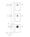
- the position of the ball-shaped tip 22 (FAB) may not be aligned with the focus position 90 of the second imaging unit 40, In this case, by moving the bonding tool 18 in the vertical direction along the Z-axis direction so that the ball-shaped tip 22 of the bonding tool 18 matches the focus position 90 with respect to the second imaging unit 40, the second The image information of the ball-shaped tip 22 can be acquired by the imaging unit 40. In the example shown in FIG.
- bonding parameters for example, the heating temperature of the ball tip 22 and the flow rate of the reducing gas are set). Etc., the control can be fed back during the wire bonding process.
- the position of the reference member 50 is detected by the second imaging unit 40 disposed on the opposite side of the reference surface S from the bonding tool 18 and the first imaging unit 30.
- the position of the ball-like tip 22 of the wire 20 is detected. Since the position of the ball-shaped tip portion 22 is detected by the second imaging unit 40, the position detection is not hindered by, for example, foreign matter attached to the bonding tool 18, and the deformation of the bonding tool 18 that is a consumable item is prevented. There is no problem of a decrease in accuracy, and the position of the bonding tool 18 in the XY axis direction can be detected with a small number of processes. Further, the position of the ball-shaped tip 22 with respect to the position of the reference member 50 can be measured more easily (for example, simultaneously by one detection) by the second imaging unit 40. Therefore, the offset for wire bonding can be measured easily and accurately. *
- the ball-shaped tip 22 of the wire 20 is detected from the side opposite to the reference plane S (that is, the lower side in the Z-axis direction), the ball-shaped tip 22 is too small to be below the bonding tool 18. Even when it does not protrude from the side end face, the ball-shaped tip 22 can be easily detected.
- the second imaging unit 40 can detect and measure the diameter and shape of the ball-shaped tip 22 or its oxidation level, it is possible to perform wire bonding with higher accuracy and higher bondability. . *
- FIG. 12 is not limited to the above-described embodiment, and can be variously modified and applied.
- FIG. 13, FIG. 14 (A) and FIG. 14 (B), and FIG. 15 are views showing modifications of the reference member.
- FIG. 15 is views showing modifications of the reference member.
- the reference member 150 includes a base 152 and a cover 156, and the metal film 158 as the second mark is outside the range surrounded by the tapered surface 154 as the first mark. Is formed. Even in such a mode, the first mark and the second mark can be provided close to each other.
- the cover 156 extends so as to reach a base 152 that is an example of an optical path length correction unit, and the optical path from the second imaging unit to the ball-shaped tip 22 has a combined thickness of the base 152 and the cover 156. It is configured to pass through a2. *
- the reference member 250 has a base 252 having a conical shape or a pyramid shape, and the outer wall side surface of the base 252 is formed as a tapered surface 254 that is a first mark, and the outer edge of the base 252 258 (side or apex of the upper surface of the base 252) functions as a second mark.
- the optical path from the second imaging unit to the ball-shaped tip 22 is configured to pass through a thickness a3 at a substantially central portion of the base 252.
- the tapered surface 254 as the first mark may be a forward taper in which the lower surface of the base 252 has a smaller area than the upper surface, or a reverse taper opposite to that. There may be.
- the reference member 350 has a base 352, an opening hole is formed in the base 352, and a tapered surface 354 having a reverse taper is formed inside the opening hole. .
- the tapered surface 354 is inclined in the direction in which the opening hole becomes wider on the lower side in the Z-axis direction.
- the first mark is not limited to the tapered surface, and may be a step 454 as shown in FIG.
- the reference member 450 has a base 452, an opening hole is formed in the base 452, and a step 454 is formed inside the opening hole.
- the step 454 includes a first surface 454a parallel to the Z-axis direction and a second surface 454b that intersects (for example, intersects with) the Z-axis direction, and is provided with a plurality of second surfaces 454b. It is possible to deal with different focus positions in the Z-axis direction of the imaging unit 30. *
- the second imaging unit 40 may detect the position of the ball-shaped tip portion 22 of the bonding tool 18 without using the reference member 550 (optical path length correction unit).
- the reference member 550 has a base 552 and a cover 556, and the metal film 558 as the second mark is formed outside the range surrounded by the tapered surface 554 as the first mark.
- the second imaging unit 40 detects the position of the ball-shaped tip 22 of the bonding tool 18 without using the reference member 550 and also detects the position of the metal film 558 that is the second mark.
- the bonding tool 18 is lowered to the height Z3 that is a focus position by the second imaging unit 40, and the ball-shaped tip 22 and the reference member 550 are moved.
- the detection process by the second imaging unit 40 may be performed in a state where the metal film 558 is aligned with the same height Z3. According to this, the configuration of the reference member can be further simplified. Further, in the wire bonding apparatus 10, the Z-axis drive of the bonding tool 18 is easy, so that the focus position can be easily adjusted. *
- Embodiments described through the embodiments of the present invention can be used in appropriate combination according to the application, or can be used with modifications or improvements, and the present invention is not limited to the description of the above-described embodiments. Absent. It is apparent from the description of the scope of claims that the embodiments added with such combinations or changes or improvements can be included in the technical scope of the present invention.
Landscapes
- Engineering & Computer Science (AREA)
- Mechanical Engineering (AREA)
- Wire Bonding (AREA)
- Manufacturing & Machinery (AREA)
- Length Measuring Devices By Optical Means (AREA)
Abstract
Description
向として説明する。
0とのオフセットが経時的に変化しておらず、前回測定のオフセットのままであると、ボンディングツール18をリファレンス部材50の方向へ移動させると、ボンディングツール18の軸心18aは、ボンディングツール18の移動前の第1撮像部30の光軸30aと一致することになる。しかしながら、現実には、ワイヤボンディングの処理を行い続けることに伴う様々な要因により、このオフセットは経時的に変化するため、両者は互いに一致せず、ずれて配置されることになり、オフセットの変化がもたらされることになる。
ース252の外縁258(ベース252の上面の辺又は頂点)は第2マークとして機能する。第2撮像部からのボール状先端部22への光路は、ベース252の略中央部の厚さa3を通過するように構成されている。なお、第1マークであるテーパ面254は、図示するように、ベース252の下面がその上面に比べて面積が小さくなる向きの順テーパであってもよいし、あるいはそれとは反対の逆テーパであってもよい。
Claims (14)
- 基準面上のボンディング対象の位置を検出する第1撮像部と、 前記第1撮像部から離間して設けられたボンディングツールと、 前記ボンディングツール及び前記第1撮像部を前記基準面に平行な方向に一体的に移動させる移動機構と、 リファレンス部材と、 前記基準面に対して前記ボンディングツール及び前記第1撮像部とは反対側に配置された第2撮像部と、 前記ボンディングツールと前記第1撮像部との間のオフセットを測定する制御部と、を備え、 前記ボンディングツールには、ワイヤが挿通され、当該ワイヤのボール状先端部が延出されており、 前記第1撮像部は、前記リファレンス部材の位置に対する前記第1撮像部の光軸の位置を検出し、 前記第2撮像部は、予め記憶されたオフセット値に従って前記ボンディングツールを前記リファレンス部材の上方に移動させたとき、前記リファレンス部材の位置を検出するとともに、前記ワイヤの前記ボール状先端部の位置を検出し、 前記制御部は、前記第1撮像部及び前記第2撮像部による各検出結果に基づいて、前記ボンディングツールと前記第1撮像部との間のオフセットの変化を測定する、ワイヤボンディング装置。
- 前記リファレンス部材は、前記第1撮像部によって検出される第1マークと、前記第2撮像部によって検出される第2マークとを有する、請求項1記載のワイヤボンディング装置。
- 前記第1マークは、前記リファレンス部材のテーパ面である、請求項2記載のワイヤボンディング装置。
- 前記第1マークは、前記リファレンス部材の段差である、請求項2記載のワイヤボンディング装置。
- 前記リファレンス部材は、前記テーパ面又は前記段差によって囲まれた開口底部を有し、 前記第2マークは、前記開口底部に形成された、請求項3又は4に記載のワイヤボンディング装置。
- 前記ワイヤの前記ボール状先端部に、前記ボンディングツールとは反対側から、前記基準面に平行なXY軸方向の各スリット光を照射する照射部をさらに含み、 前記制御部は、前記XY軸方向の各スリット光に基づいて、前記ボンディングツールと前記第1撮像部との間のオフセットの変化を測定する、請求項1から5のいずれか一項に記載のワイヤボンディング装置。
- 前記制御部は、前記ボンディングツールから延出した前記ワイヤの前記ボール状先端部の径及び形状の少なくとも1つを測定する、請求項6記載のワイヤボンディング装置。
- 前記リファレンス部材は、光路長補正部を有し、 前記第2撮像部は、前記リファレンス部材の前記光路長補正部を介して前記ワイヤの前記ボール状先端部の位置を検出する、請求項1から請求項7のいずれか一項に記載のワイヤボンディング装置。
- 前記制御部は、測定した前記オフセットの変化をフィードバックし、次のワイヤボンディングに反映させる、請求項1から請求項8のいずれか一項に記載のワイヤボンディング装置。
- 前記予め記憶されたオフセット値は、前記制御部によって前回測定したオフセット値である、請求項9記載のワイヤボンディング装置。
- 前記制御部は、前記第2撮像部の検出結果に基づいて前記ワイヤの前記ボール状先端部の酸化レベルを測定する、請求項1から請求項10のいずれか一項に記載のワイヤボンディング装置。
- 前記制御部は、測定した前記酸化レベルが高い場合、ボンディングパラメータにフィードバックし、次のワイヤボンディングに反映させる、請求項11記載のワイヤボンディング装置。
- 前記第2撮像部は、前記ボンディングツールを前記基準面に対して垂直方向に移動したときの、前記ワイヤの前記ボール状先端部の移動に伴う変化を検出する、請求項11記載のワイヤボンディング装置。
- 基準面上のボンディング対象の位置をワイヤボンディングする方法であって、 ワイヤボンディング装置を準備する工程であって、前記第1撮像部から離間して設けられたボンディングツールと、前記ボンディングツール及び前記第1撮像部を前記基準面に平行な方向に一体的に移動させる移動機構と、リファレンス部材と、前記基準面に対して前記ボンディングツール及び前記第1撮像部とは反対側に配置された第2撮像部と、前記ボンディングツールと前記第1撮像部との間のオフセットを測定する制御部とを備える、ワイヤボンディング装置を準備する工程と、 前記ボンディングツールから延出されたワイヤにボール状先端部を形成する工程と、 前記第1撮像部を前記リファレンス部材の上方に移動させた後、前記第1撮像部によって前記リファレンス部材の位置に対する前記第1撮像部の光軸の位置を検出する第1検出工程と、 予め記憶されたオフセット値に従って前記ボンディングツールを前記リファレンス部材の上方に移動させた後、前記第2撮像部によって、前記リファレンス部材の位置を検出するとともに、前記ワイヤの前記ボール状先端部の位置を検出する第2検出工程と、 前記第1及び第2検出工程の各検出結果に基づいて、前記ボンディングツールと前記第1撮像部との間のオフセットの変化を測定する工程と、を含む、ワイヤボンディング方法。
Priority Applications (5)
| Application Number | Priority Date | Filing Date | Title |
|---|---|---|---|
| CN201680030547.3A CN107615465B (zh) | 2015-03-31 | 2016-03-22 | 引线接合装置以及引线接合方法 |
| SG11201710074TA SG11201710074TA (en) | 2015-03-31 | 2016-03-22 | Wire bonding apparatus and wire bonding method |
| JP2017509838A JP6461311B2 (ja) | 2015-03-31 | 2016-03-22 | ワイヤボンディング装置及びワイヤボンディング方法 |
| KR1020177030639A KR101962888B1 (ko) | 2015-03-31 | 2016-03-22 | 와이어 본딩 장치 및 와이어 본딩 방법 |
| US15/716,525 US10262968B2 (en) | 2015-03-31 | 2017-09-27 | Wire bonding apparatus and wire bonding method |
Applications Claiming Priority (2)
| Application Number | Priority Date | Filing Date | Title |
|---|---|---|---|
| JP2015-072382 | 2015-03-31 | ||
| JP2015072382 | 2015-03-31 |
Related Child Applications (1)
| Application Number | Title | Priority Date | Filing Date |
|---|---|---|---|
| US15/716,525 Continuation US10262968B2 (en) | 2015-03-31 | 2017-09-27 | Wire bonding apparatus and wire bonding method |
Publications (1)
| Publication Number | Publication Date |
|---|---|
| WO2016158588A1 true WO2016158588A1 (ja) | 2016-10-06 |
Family
ID=57005037
Family Applications (1)
| Application Number | Title | Priority Date | Filing Date |
|---|---|---|---|
| PCT/JP2016/059067 Ceased WO2016158588A1 (ja) | 2015-03-31 | 2016-03-22 | ワイヤボンディング装置及びワイヤボンディング方法 |
Country Status (6)
| Country | Link |
|---|---|
| US (1) | US10262968B2 (ja) |
| JP (1) | JP6461311B2 (ja) |
| KR (1) | KR101962888B1 (ja) |
| CN (1) | CN107615465B (ja) |
| SG (1) | SG11201710074TA (ja) |
| WO (1) | WO2016158588A1 (ja) |
Cited By (2)
| Publication number | Priority date | Publication date | Assignee | Title |
|---|---|---|---|---|
| WO2023281623A1 (ja) * | 2021-07-06 | 2023-01-12 | 株式会社新川 | 半導体装置の製造装置および製造方法 |
| US12261148B2 (en) | 2020-06-05 | 2025-03-25 | Shinkawa Ltd. | Wire bonding apparatus |
Families Citing this family (9)
| Publication number | Priority date | Publication date | Assignee | Title |
|---|---|---|---|---|
| TWI580511B (zh) * | 2014-06-10 | 2017-05-01 | 新川股份有限公司 | A bonding device, and a method of estimating the placement position of the engagement tool |
| US10658328B2 (en) * | 2017-11-09 | 2020-05-19 | Asm Technology Singapore Pte Ltd | Detection of foreign particles during wire bonding |
| JP6973831B2 (ja) * | 2019-03-08 | 2021-12-01 | 株式会社新川 | ワイヤボンディング装置 |
| JP7291586B2 (ja) * | 2019-09-19 | 2023-06-15 | ファスフォードテクノロジ株式会社 | ダイボンディング装置および半導体装置の製造方法 |
| CN116325102A (zh) * | 2021-01-26 | 2023-06-23 | 株式会社新川 | 打线接合装置、打线接合装置的控制方法以及打线接合装置的控制程序 |
| TWI818614B (zh) * | 2022-07-04 | 2023-10-11 | 日商新川股份有限公司 | 半導體裝置的製造裝置及製造方法 |
| CN117810147B (zh) * | 2024-03-01 | 2024-06-11 | 精技电子(南通)有限公司 | 一种引线键合机用芯片定位装置 |
| WO2025226499A1 (en) * | 2024-04-22 | 2025-10-30 | Kulicke And Soffa Industries, Inc. | Methods of imaging a wire structure on a wire bonding system |
| GB2642426A (en) * | 2024-05-31 | 2026-01-14 | Nordson Corp | Apparatus and method for automatically calibrating the position of a test tool of a bond tester |
Citations (2)
| Publication number | Priority date | Publication date | Assignee | Title |
|---|---|---|---|---|
| JP2000021923A (ja) * | 1998-07-03 | 2000-01-21 | Shinkawa Ltd | ボンディング方法及びその装置 |
| JP2001249007A (ja) * | 2000-03-06 | 2001-09-14 | Shinkawa Ltd | オフセット測定方法、ツール位置検出方法およびボンディング装置 |
Family Cites Families (12)
| Publication number | Priority date | Publication date | Assignee | Title |
|---|---|---|---|---|
| JP2913565B2 (ja) * | 1991-01-31 | 1999-06-28 | 株式会社新川 | ワイヤループ曲がり検査方法及びその装置 |
| JP3416091B2 (ja) * | 2000-01-21 | 2003-06-16 | 株式会社新川 | ボンディング装置およびボンディング方法 |
| JP3732082B2 (ja) * | 2000-09-25 | 2006-01-05 | 株式会社新川 | ボンディング装置およびボンディング方法 |
| JP3802403B2 (ja) * | 2001-11-27 | 2006-07-26 | 株式会社新川 | ワイヤボンディング方法及び装置 |
| JP4105926B2 (ja) * | 2002-09-30 | 2008-06-25 | 株式会社新川 | ボンディング装置におけるオフセット測定機構及びボンディング装置におけるオフセット測定方法 |
| JP3836479B2 (ja) | 2004-07-01 | 2006-10-25 | 株式会社カイジョー | ワイヤボンディング装置 |
| CN101052493A (zh) * | 2004-09-22 | 2007-10-10 | 库利克和索夫工业公司 | 用于引线接合机接合头的运动控制装置 |
| JP4530984B2 (ja) * | 2005-12-28 | 2010-08-25 | 株式会社新川 | ワイヤボンディング装置、ボンディング制御プログラム及びボンディング方法 |
| JP4264458B1 (ja) * | 2008-06-13 | 2009-05-20 | 株式会社新川 | 圧着ボール径検出装置および方法 |
| JP5117462B2 (ja) * | 2009-09-18 | 2013-01-16 | 株式会社新川 | ワイヤボンディング装置及び方法 |
| KR101404516B1 (ko) * | 2012-10-29 | 2014-06-10 | 한미반도체 주식회사 | 전자부품 실장장치의 교정방법 |
| KR101598999B1 (ko) * | 2012-11-16 | 2016-03-02 | 가부시키가이샤 신가와 | 와이어 본딩 장치 및 반도체 장치의 제조 방법 |
-
2016
- 2016-03-22 WO PCT/JP2016/059067 patent/WO2016158588A1/ja not_active Ceased
- 2016-03-22 SG SG11201710074TA patent/SG11201710074TA/en unknown
- 2016-03-22 JP JP2017509838A patent/JP6461311B2/ja active Active
- 2016-03-22 CN CN201680030547.3A patent/CN107615465B/zh active Active
- 2016-03-22 KR KR1020177030639A patent/KR101962888B1/ko active Active
-
2017
- 2017-09-27 US US15/716,525 patent/US10262968B2/en active Active
Patent Citations (2)
| Publication number | Priority date | Publication date | Assignee | Title |
|---|---|---|---|---|
| JP2000021923A (ja) * | 1998-07-03 | 2000-01-21 | Shinkawa Ltd | ボンディング方法及びその装置 |
| JP2001249007A (ja) * | 2000-03-06 | 2001-09-14 | Shinkawa Ltd | オフセット測定方法、ツール位置検出方法およびボンディング装置 |
Cited By (4)
| Publication number | Priority date | Publication date | Assignee | Title |
|---|---|---|---|---|
| US12261148B2 (en) | 2020-06-05 | 2025-03-25 | Shinkawa Ltd. | Wire bonding apparatus |
| WO2023281623A1 (ja) * | 2021-07-06 | 2023-01-12 | 株式会社新川 | 半導体装置の製造装置および製造方法 |
| JP7253862B1 (ja) * | 2021-07-06 | 2023-04-07 | 株式会社新川 | 半導体装置の製造装置および製造方法 |
| US12374650B2 (en) | 2021-07-06 | 2025-07-29 | Shinkawa Ltd. | Manufacturing apparatus and manufacturing method of semiconductor device |
Also Published As
| Publication number | Publication date |
|---|---|
| CN107615465B (zh) | 2020-05-12 |
| JPWO2016158588A1 (ja) | 2018-02-08 |
| CN107615465A (zh) | 2018-01-19 |
| US20180090464A1 (en) | 2018-03-29 |
| JP6461311B2 (ja) | 2019-01-30 |
| KR20170129936A (ko) | 2017-11-27 |
| KR101962888B1 (ko) | 2019-03-27 |
| US10262968B2 (en) | 2019-04-16 |
| SG11201710074TA (en) | 2018-01-30 |
Similar Documents
| Publication | Publication Date | Title |
|---|---|---|
| JP6461311B2 (ja) | ワイヤボンディング装置及びワイヤボンディング方法 | |
| JP7018341B2 (ja) | ダイボンディング装置および半導体装置の製造方法 | |
| TWI655406B (zh) | 接合裝置以及被攝體的高度檢測方法 | |
| TWI580511B (zh) | A bonding device, and a method of estimating the placement position of the engagement tool | |
| US20170148759A1 (en) | Bonding apparatus and bonding method | |
| CN101925991B (zh) | 焊接装置及焊接装置的焊接台高度调整方法 | |
| JP2003163243A (ja) | ワイヤボンディング方法及び装置 | |
| JP2015190826A (ja) | 基板検査装置 | |
| CN111279462B (zh) | 接合装置 | |
| JP2008207244A (ja) | 接合装置の検出対象物の検出方法、接合装置及び接合方法 | |
| JPH09312302A (ja) | コンポーネントの位置合せ方法とシステム | |
| JP2005268486A (ja) | マーキング方法及びマーキング装置並びに検査装置 | |
| JP2010267756A (ja) | ボンディング装置及びボンディング方法 | |
| JP2014036068A (ja) | ダイボンダおよびボンディングツールの位置検出方法 | |
| JP6047723B2 (ja) | ダイボンダおよびボンディングツールと半導体ダイとの相対位置の検出方法 | |
| JP6182248B2 (ja) | ダイボンダ | |
| JP3008745B2 (ja) | ワイヤボンディング検査方法及びワイヤボンディング検査装置 | |
| JP2009166052A (ja) | 導電性部材溶着装置 | |
| JP2006210785A (ja) | 半導体位置合わせ装置および位置合わせ方法 | |
| JPH10112469A (ja) | ワイヤボンディング検査装置 | |
| JP2000286452A (ja) | 発光素子の発光中心検出方法 | |
| JP5200774B2 (ja) | 検査装置及び方法 | |
| JP2008041758A (ja) | フラックスの転写状態検査方法及び装置 | |
| JPH11214428A (ja) | ボンディング装置 | |
| JP2000353900A (ja) | 電子部品の実装方法および位置認識用の標体 |
Legal Events
| Date | Code | Title | Description |
|---|---|---|---|
| 121 | Ep: the epo has been informed by wipo that ep was designated in this application |
Ref document number: 16772469 Country of ref document: EP Kind code of ref document: A1 |
|
| ENP | Entry into the national phase |
Ref document number: 2017509838 Country of ref document: JP Kind code of ref document: A |
|
| NENP | Non-entry into the national phase |
Ref country code: DE |
|
| ENP | Entry into the national phase |
Ref document number: 20177030639 Country of ref document: KR Kind code of ref document: A |
|
| WWE | Wipo information: entry into national phase |
Ref document number: 11201710074T Country of ref document: SG |
|
| 122 | Ep: pct application non-entry in european phase |
Ref document number: 16772469 Country of ref document: EP Kind code of ref document: A1 |