WO2016158068A1 - 半導体レーザ装置及びその製造方法 - Google Patents
半導体レーザ装置及びその製造方法 Download PDFInfo
- Publication number
- WO2016158068A1 WO2016158068A1 PCT/JP2016/054858 JP2016054858W WO2016158068A1 WO 2016158068 A1 WO2016158068 A1 WO 2016158068A1 JP 2016054858 W JP2016054858 W JP 2016054858W WO 2016158068 A1 WO2016158068 A1 WO 2016158068A1
- Authority
- WO
- WIPO (PCT)
- Prior art keywords
- semiconductor laser
- submount
- laser element
- layer
- solder layer
- Prior art date
- Legal status (The legal status is an assumption and is not a legal conclusion. Google has not performed a legal analysis and makes no representation as to the accuracy of the status listed.)
- Ceased
Links
Images




Classifications
-
- H—ELECTRICITY
- H01—ELECTRIC ELEMENTS
- H01S—DEVICES USING THE PROCESS OF LIGHT AMPLIFICATION BY STIMULATED EMISSION OF RADIATION [LASER] TO AMPLIFY OR GENERATE LIGHT; DEVICES USING STIMULATED EMISSION OF ELECTROMAGNETIC RADIATION IN WAVE RANGES OTHER THAN OPTICAL
- H01S5/00—Semiconductor lasers
- H01S5/02—Structural details or components not essential to laser action
- H01S5/022—Mountings; Housings
- H01S5/0239—Combinations of electrical or optical elements
-
- H—ELECTRICITY
- H01—ELECTRIC ELEMENTS
- H01S—DEVICES USING THE PROCESS OF LIGHT AMPLIFICATION BY STIMULATED EMISSION OF RADIATION [LASER] TO AMPLIFY OR GENERATE LIGHT; DEVICES USING STIMULATED EMISSION OF ELECTROMAGNETIC RADIATION IN WAVE RANGES OTHER THAN OPTICAL
- H01S5/00—Semiconductor lasers
- H01S5/02—Structural details or components not essential to laser action
- H01S5/024—Arrangements for thermal management
Definitions
- the present invention relates to a semiconductor laser device and a manufacturing method thereof.
- a large amount of heat is generated during driving. Due to the temperature change due to this heat generation, the oscillation wavelength and emission intensity of the semiconductor laser element change. Therefore, it is important how efficiently the heat generated when the semiconductor laser element is driven is discharged.
- a submount is formed using a material having high thermal conductivity, and the semiconductor laser element is formed on the submount. Technologies for discharging the generated heat have been proposed.
- a solder layer is formed between the submount and the semiconductor laser element, the solder layer is heated and melted, and then cooled and solidified to join the submount and the semiconductor laser element.
- Cu and Cu—W alloys are examples of materials having high thermal conductivity that are used as submounts, and both of these exhibit values of thermal conductivity exceeding 200 W / m ⁇ K.
- the linear expansion coefficient of these materials does not match the linear expansion coefficient of the constituent material of the semiconductor laser element.
- the linear expansion coefficient of a GaAs substrate generally used as a semiconductor laser element is 6.6 ⁇ 10 ⁇ 6 / K.
- the linear expansion coefficient of Cu described above as the material of the submount, Cu-W alloy (Cu20%) are each 18 ⁇ 10 -6 /K,8.3 ⁇ 10 -6 / K , both The value is larger than the linear expansion coefficient of GaAs.
- the Cu—W alloy has a linear expansion coefficient close to that of GaAs compared to Cu.
- a Cu—W alloy of 10% Cu has a linear expansion coefficient of 6.4 ⁇ 10 ⁇ 6 / K.
- the manufacturing cost of the semiconductor laser device is extremely increased.
- Patent Document 1 discloses a technique for suppressing warpage of a semiconductor laser element after bonding while using a cheaper AlN without using a Cu—W alloy as a material for the submount. ing. More specifically, the submount is made of AlN, and a coating layer made of Cu plating is formed on the main surface and the back surface of the submount with a predetermined thickness. Thereby, since the linear expansion coefficient of the entire submount can be made substantially equal to the linear expansion coefficient of the semiconductor laser element, the warpage of the semiconductor laser element after bonding to the submount can be reduced.
- a solder layer made of Au—Sn solder is formed on the upper surface of the coating layer formed on the main surface of the submount, and the semiconductor laser element and the submount on which the coating layer is formed are joined. ing.
- An object of the present invention is to realize a semiconductor laser device in which warpage occurring in a semiconductor laser element and a submount is further suppressed as compared with the conventional one.
- the semiconductor laser device of the present invention is A submount, Material layers respectively formed on two opposing surfaces of the submount; A solder layer formed on one of the material layers; A semiconductor laser element formed in an upper layer of the solder layer, The opposing region where the submount and the semiconductor laser element face each other is a first region including both the material layer and the solder layer with respect to a first direction orthogonal to the surface of the submount, and the material layer or the And a second region including one or both of the solder layers.
- the semiconductor laser element has a shape in which the length in the second direction orthogonal to the first direction is longer than the length in the third direction orthogonal to the first direction and the second direction with respect to the first direction.
- the second region may have a shape in which the length in the third direction is longer than the length in the second direction with respect to the first direction.
- the semiconductor element has a shape in which the second direction is the longitudinal direction and the third direction is the short direction, and for example, a plurality of emitters that emit laser light are arranged in the longitudinal direction (second direction).
- the second region included in the facing region has a shape in which the short side direction is longer than the long side direction in the first direction, that is, the direction orthogonal to the surface of the submount. According to the above configuration, in the array-type semiconductor laser element, it is possible to suppress warping that occurs in the semiconductor laser element and the submount.
- the second region may have a shorter length in the third direction than the first region.
- the material layer is When the semiconductor laser element is made of a material having a larger linear expansion coefficient than the submount, the semiconductor laser element is made of a material having a larger linear expansion coefficient than the submount, When the semiconductor laser element is made of a material having a smaller linear expansion coefficient than the submount, the semiconductor laser element may be made of a material having a smaller linear expansion coefficient than the submount.
- the linear expansion coefficient of the entire submount should be made larger by forming a material layer than before formation. Can do. Further, when the semiconductor laser element is made of a material having a smaller linear expansion coefficient than that of the submount, by forming the material layer, the linear expansion coefficient of the entire submount can be made smaller than before formation. . Thereby, the linear expansion coefficient of the whole submount can be brought close to the linear expansion coefficient of the semiconductor laser element.
- a method for manufacturing a semiconductor laser device of the present invention includes: Preparing a submount (a); Forming a material layer on each of the two opposing surfaces of the submount (b); A step (c) of forming a solder layer on one of the material layers; A step (d) of forming a semiconductor laser element on an upper layer of the solder layer by heating and melting the solder layer and then cooling and solidifying the solder layer; In the steps (b) and (c), with respect to a first direction orthogonal to the surface of the submount, a first region including both the material layer and the solder layer, and one of the material layer and the solder layer are formed. A step of forming the material layer and the solder layer so as to have a second region including or not including both, The step (d) includes a step of forming the semiconductor laser element so as to extend over both the first region and the second region.
- the step (b) is a step of forming the material layer on one of the two surfaces of the submount discretely or with a gap.
- a solder layer may be formed on the upper surface of the material layer formed on the one surface.
- the material layer and the solder layer can be formed so as to have the first region including both the material layer and the solder layer and the second region not including at least the material layer. More specifically, a first region that includes both the material layer and the solder layer, a second region that includes the solder layer and does not include the material layer, or a second region that does not include both the solder layer and the material layer, The material layer and the solder layer can be formed to have
- the semiconductor laser device of the present invention it is possible to further suppress the warpage generated in the semiconductor laser element and the submount than before.
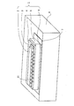
- 1 is a schematic perspective view of a semiconductor laser device according to a first embodiment.
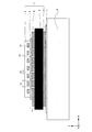
- 1 is a schematic front view of a semiconductor laser device according to a first embodiment. It is the figure which abbreviate
- FIG. 1 schematically shows a perspective view of a semiconductor laser device 1 in the present embodiment.
- the semiconductor laser device 1 includes a semiconductor laser element 2, a first solder layer 3, a first material layer 4, a submount 5, and a second material layer 6.
- the semiconductor laser element 2 is an edge-emitting semiconductor laser element in which an emitter 21 that emits laser light is disposed on the end face of the semiconductor laser element 2.
- the first solder layer 3 is a layer for joining the semiconductor laser element 2 and the submount 5 formed on the two surfaces where the first material layer 4 and the second material layer 6 face each other.
- the first solder layer 3 is made of, for example, Au—Sn solder.
- the first material layer 4, the submount 5, and the second material layer 6 will be described later.
- the second solder layer 7 is a layer for joining the heat sink 8 and the submount 5 formed on the two surfaces where the first material layer 4 and the second material layer 6 face each other.
- the second solder layer 7 is made of, for example, Sn—Ag—Cu solder.
- the heat sink 8 is formed of a material having high thermal conductivity such as Cu.
- FIG. 2 is a schematic view of the semiconductor laser device 1 bonded to the heat sink 8 through the second solder layer 7 with the emitter 21 facing the front.
- the second solder layer 7 is formed on the main surface of the heat sink 8.
- a first material layer 4 and a second material layer 6 are formed on the main surface and the back surface of the submount 5, respectively.
- the submount 5 on which the first material layer 4 and the second material layer 6 are formed is formed on the second solder layer 7.
- a first solder layer 3 is formed on the upper surface of the first material layer 4.
- a semiconductor laser element 2 is formed on the upper surface of the first solder layer 3.
- the semiconductor laser element 2 is a semiconductor element that oscillates light and oscillates laser light.
- the semiconductor laser element 2 is an array type semiconductor laser element in which a plurality of emitters 21 are arranged in the longitudinal direction.
- the longitudinal direction of the semiconductor laser element 2 is defined as the X direction
- the lateral direction is defined as the Y direction
- the thickness direction is defined as the Z direction.
- the Z direction corresponds to the “first direction”
- the X direction corresponds to the “second direction”
- the Y direction corresponds to the “third direction”.
- 40 emitters 21 are arranged in the X direction. In FIGS. 1 and 2, some of the emitters 21 are not shown.
- the semiconductor laser element 2 will be described as being composed of GaAs.
- the main surface is a surface on the semiconductor laser element 2 side in the Z direction, and the back surface is a surface opposite to the main surface.
- a void 10 is formed in the first solder layer 3 and the first material layer 4. As shown in FIG. 2, the depth of the gap 10, that is, the length in the Z direction is equal to the thickness of the first solder layer 3 and the first material layer 4. That is, the void 10 penetrates the first solder layer 3 and the first material layer 4.
- the void 10 is a space where there is no Au—Sn solder, which is a constituent material of the first solder layer 3, and Cu, which is a constituent material of the first material layer 4.
- the submount 5 is made of a material having high thermal conductivity.
- the submount 5 is made of AlN.
- the coefficient of linear expansion of AlN is 4.6 ⁇ 10 ⁇ 6 / K, which is smaller than the coefficient of linear expansion of GaAs, which is a constituent material of the semiconductor laser element 2 6.6 ⁇ 10 ⁇ 6 / K.
- the semiconductor laser element 2 is directly joined to the upper surface of the submount 5 made of AlN via the first solder layer 3, the semiconductor is caused by the difference in linear expansion coefficient between the submount 5 and the semiconductor laser element 2.
- the laser element 2 may be warped.
- the first material layer 4 and the second material layer 6 made of a material having a linear expansion coefficient larger than that of AlN are formed on the main surface and the back surface of the submount 5, respectively.
- the first material layer 4 and the second material layer 6 can be made of Cu, for example.
- the linear expansion coefficient of Cu is 18 ⁇ 10 ⁇ 6 / K, which is larger than the linear expansion coefficient of AlN and that of GaAs.
- the facing region 9 where the semiconductor laser element 2 and the submount 5 face each other includes a first region 12 including both the first solder layer 3 and the first material layer 4 and a second region 13 not including both in the Z direction. And have.
- the second region 13 is composed of the gap 10.
- the description will be continued by taking as an example the case where the gap 10 is provided at an equal interval to the interval at which the emitters 21 are arranged.
- FIG. 3 schematically shows a plan view of the semiconductor laser device 1 according to the present embodiment when viewed from the semiconductor laser element 2 toward the submount 5.
- the illustration of the semiconductor laser element 2 is omitted for convenience of explanation.
- the gap 10 penetrates the first solder layer 3 and the first material layer 4. Therefore, as shown in FIG. 3, when the semiconductor laser device 1 is viewed from the semiconductor laser element 2 toward the submount 5, the main surface of the submount 5 appears through the gap 10.
- the main surface of the submount 5 that appears through the gap 10 is referred to as an exposed surface 14.
- the exposed surface 14 is a rectangular surface.
- the length of the exposed surface 14 in the Y direction is longer than the length in the X direction. Further, the length of the exposed surface 14 in the Y direction is shorter than the lengths of the first solder layer 3 and the first material layer 4 in the Y direction. That is, the first solder layer 3 and the first material layer 4 can be expressed as being cut out in a part in the short direction. In the present embodiment, the length of the exposed surface 14 in the Y direction is half the length of the first solder layer 3 in the Y direction.
- the air gap 10 is formed on the end face side where the emitter 21 is disposed.
- the ball-shaped solder is confined in the empty wall 10 even if the solder material has a ball shape. be able to. This prevents the laser beam emitted from the emitter 21 from being blocked, and the ball-shaped solder hinders the lens assembly when a lens with a very short focal length of about several tens of microns is attached. Can be prevented.
- the submount 5 is prepared. Specifically, an AlN substrate having a thickness of 250 ⁇ m is prepared. This step corresponds to step (a).
- the main surface and the back surface of the submount 5 are plated with Cu to form the first material layer 4 and the second material layer 6.
- the main surface of the submount 5 is subjected to Cu plating by masking a range of the gap 10 to be formed in the first material layer 4 with a resist.
- the back surface of the submount 5 the entire back surface is plated with Cu.
- the thickness of the 1st material layer 4 and the 2nd material layer 6 is 75 micrometers. This step corresponds to step (b).
- the first solder layer 3 is formed on the upper surface of the first material layer 4 formed in the step (b).
- This step corresponds to step (c).
- the void 10 can be formed in the first solder layer 3 and the first material layer 4. That is, with respect to the Z direction, the first region 12 including both the first solder layer 3 and the first material layer 4 and the second region 13 not including both the first solder layer 3 and the first material layer 4 are included. As described above, the first solder layer 3 and the first material layer 4 can be formed.
- the semiconductor laser element 2 is placed on the upper surface of the first solder layer 3. Then, after the first solder layer 3 is heated and melted, the semiconductor laser element 2, the first material layer 4 and the second material layer 6 are formed on two opposing surfaces by cooling to about room temperature and solidifying. The submount 5 is joined. This step corresponds to step (d).
- the heating step may be started before the semiconductor laser element 2 is placed on the upper layer of the first solder layer 3.
- Examples 1 to 3 are examples of the semiconductor laser device 1 according to the present embodiment. More specifically, Example 3 is a semiconductor laser device in which gaps 10 are provided in the first solder layer 3 and the first material layer 4 at intervals at which the emitters 21 are arranged in the X direction. That is, in Example 3, the interval between the emitters 21 and the interval between the gaps 10 are equal in the X direction.
- Example 1 is a semiconductor laser device in which gaps 10 are provided in the first solder layer 3 and the first material layer 4 at intervals four times that of Example 3.
- Example 2 is a semiconductor laser device in which gaps 10 are provided in the first solder layer 3 and the first material layer 4 at twice the interval as in Example 3.
- the comparative example is a semiconductor laser device in which no gap 10 is provided in the first solder layer 3 and the first material layer 4.
- the number of voids 10 is as follows: Example 3> Example 2> Example 1> Comparative Example.
- step (b) described in [Manufacturing method] is different, and steps (a), (c), and (d) are common. More specifically, the number of masking portions in the Cu plating in the step (b) is different, and the number is as follows: Example 3> Example 2> Example 1> Comparative Example. That is, as the number of masking portions increases, the number of voids 10 increases. In the comparative example, Cu plating is performed without masking, and the number of voids 10 is zero. That is, Cu is formed on the entire main surface of the submount 5.
- the semiconductor laser element 2 is warped in line symmetry with respect to the Z axis. Therefore, FIG. 4 shows only the Z coordinate when X ⁇ 0.
- the Z coordinate at the center of the semiconductor laser element 2 is shifted from 0 to a negative value. It can be seen that the Z coordinate increases as the X coordinate moves away from the center.
- the Z coordinate of the center of the semiconductor laser element 2 is ⁇ 1.4 ⁇ m. Further, when the X coordinate is ⁇ 4 mm, the Z coordinate is 2.8 ⁇ m, and the difference from the center Z coordinate is 4.2 ⁇ m, which indicates that the semiconductor laser element 2 and the submount 5 are greatly warped. .
- Example 1 the Z coordinate of the center of the semiconductor laser element 2 is ⁇ 1.4 ⁇ m.
- the Z coordinate is 2.3 ⁇ m, and the difference from the center Z coordinate is 3.7 ⁇ m. It can be seen that the warpage of Example 1 is suppressed compared to the comparative example.
- Example 2 the Z coordinate of the center of the semiconductor laser element 2 is ⁇ 1.4 ⁇ m.
- the Z coordinate is 1.3 ⁇ m, and the difference from the central Z coordinate is 2.7 ⁇ m. It can be seen that the warpage of Example 2 is further suppressed as compared to Example 1.
- Example 3 the Z coordinate of the center of the semiconductor laser element 2 is ⁇ 1.2 ⁇ m.
- the Z coordinate is ⁇ 0.4 ⁇ m, and the difference from the central Z coordinate is 0.8 ⁇ m. It can be seen that the warpage is further suppressed in Example 3 compared to Example 2.
- the first to third embodiments can suppress the warpage generated in the semiconductor laser element 2 and the submount 5 as compared with the comparative example. Moreover, compared with Example 1, Example 2 can further suppress warpage, and compared with Example 2, Example 3 can further suppress warpage. That is, as the number of voids 10 formed in the first solder layer 3 and the first material layer 4 increases, the warpage of the semiconductor laser element 2 and the submount 5 can be suppressed.
- the semiconductor laser element 2 and the submount 5 warp so as to protrude in the direction from the semiconductor laser element to the submount 5.
- the linear expansion coefficient on the semiconductor laser element 2 side when the center of the submount 5 is divided in the Z direction is defined as Su
- the linear expansion coefficient on the submount 5 side is defined as Sl.
- the semiconductor laser element 2 side when the center of the submount 5 is divided into two in the Z direction is referred to as an upper side
- the submount 5 side is referred to as a lower side.
- FIG. 5 schematically shows a diagram for explaining Su and Sl.
- FIG. 5 shows a semiconductor laser device 15 in a comparative example.
- FIG. 5 shows a state in which the semiconductor laser element 2 and the submount 5 are not warped for convenience of explanation, but actually the semiconductor laser element 2 and the submount 5 are warped so as to protrude downward.
- FIG. 6 schematically shows a state where the semiconductor laser device 15 of the comparative example is warped.
- the semiconductor laser device 15 includes a semiconductor laser element 2, a first solder layer 16, a first material layer 17, a submount 5, and a second material layer 6.
- the semiconductor laser device 15 of the comparative example is different from the semiconductor laser device 1 of the present embodiment in that the gap 10 is not formed in the first solder layer 16 and the first material layer 17, but the other configurations are the same.
- Su is an integral linear expansion coefficient of the semiconductor laser element 2, the first solder layer 16, the first material layer 17, and a portion located above the submount 5.
- S1 is an integral linear expansion coefficient of the second material layer 6 and a portion located below the submount 5.
- the first material layer 17 and the second material layer 6 are formed on the two surfaces of the submount 5 by Cu plating, the first material layer 17 and the second material layer 6 cannot be shrunk in accordance with their physical properties. Therefore, the first solder layer 16 formed on the upper surface of the first material layer 17 is also affected by the first material layer 17 and cannot shrink according to the physical property values.
- the first material layer 17 and the second material layer 6 are formed on the main surface and the back surface of the submount 5 and the linear expansion coefficient of the entire submount 5 is brought close to the linear expansion coefficient of the semiconductor laser element 2,
- the thickness of the 1st material layer 17 and the 2nd material layer 6 becomes comparatively thick.
- the first material layer 17 and the second material layer 6 can freely contract as the thickness increases. This is because portions of the first material layer 17 and the second material layer 6 that are relatively far from the submount 5 are not easily affected by the submount 5.
- the first solder layer 16 formed on the upper surface of the first material layer 17 can also freely contract, and the contraction amount of the first solder layer 16 increases.
- Su has a larger value than Sl, and the upper shrinkage amount is larger than the lower shrinkage amount. Therefore, as shown in FIG. 6, the upper radius of curvature r1 is smaller than the lower radius of curvature r2, so that the semiconductor laser element 2 and the submount 5 protrude downward, that is, protrude downward. Warp.
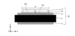
- FIG. 7A is a schematic view of the semiconductor laser device 15 in the comparative example viewed from the front side of the emitter 21.
- FIG. 7B is a schematic view of the semiconductor laser device 1 according to the present embodiment as viewed from the front side of the emitter 21.
- the semiconductor laser device 1 in the present embodiment will be described by taking as an example a case where two voids 10 are formed in the first solder layer 3 and the first material layer 4. Further, when the semiconductor laser device 1 according to the present embodiment is viewed with the emitter 21 in front, the surface formed by the cutouts of the first solder layer 3 and the first material layer 4 appears through the gap 10, but FIG. However, illustration of this surface is omitted for convenience of explanation. 7A and 7B show a state where the semiconductor laser element 2 and the submount 5 are not warped for convenience of explanation.
- the first solder layer 16 contracts around P1. More specifically, as shown in FIG. 7A, if the first solder layer 16 is divided into the first solder layers 16a and 16b by dividing the first solder layer 16 in the X direction for convenience, the first solder layers 16a and 16b are: Shrinks toward P1.
- the first solder layer 3 in the semiconductor laser device 1 has a half length in the Y direction cut away by the gap 10. If the first solder layer 3 is divided into two in the Y direction and divided into a portion having a void and a portion not having a void, the shrinkage of the portion having a void is caused by each of the first solder layers 3a, 3b, and 3c. It can be thought of as contraction. The first solder layers 3a, 3b, and 3c contract around the center P2 in the respective X, Y, and Z directions.
- the amount of shrinkage in the longitudinal direction increases in proportion to the length in the longitudinal direction.
- the length of the first solder layer 16 in the longitudinal direction (that is, the X direction) is d1.
- the lengths of the first solder layers 3a, 3b, and 3c in the longitudinal direction are d2, d3, and d4.
- d2, d3, and d4 are each shorter than d1. Therefore, the shrinkage amount of each of the first solder layers 3a, 3b, and 3c is smaller than the shrinkage amount of the portion having no void.
- the shrinkage amount of the first solder layer 3 in the present embodiment is smaller than the shrinkage amount of the first solder layer 16 in the comparative example.
- the difference in length in the longitudinal direction of the first solder layer affects the shrinkage.
- the shrinkage amount of the first solder layer 3 can be reduced as compared with the comparative example, and therefore the value of Su can also be reduced as compared with the comparative example.
- the difference of Su and Sl can be made small compared with a comparative example. As a result, the difference in shrinkage between the upper side and the lower side is reduced, and warpage can be suppressed.
- the above-mentioned warp appears particularly conspicuously in the array type semiconductor laser element as in the present embodiment.
- the length of the first solder layer in the longitudinal direction is relatively long. Therefore, it is considered that the shrinkage amount of the first solder layer becomes relatively large, Su increases, and the difference between Su and Sl becomes relatively large.
- FIG. 8 schematically shows a plan view of the semiconductor laser device 1 according to the present embodiment when viewed in the direction from the semiconductor laser element 2 toward the submount 5.
- the illustration of the semiconductor laser element 2 is omitted for convenience of explanation.
- the void 10 penetrates the first solder layer 3 and the first material layer 4 as in the first embodiment. Therefore, as shown in FIG. 8, the main surface of the submount 5, that is, the exposed surface 14 appears through the gap 10.
- the length of the exposed surface 14 in the Y direction is equal to the length of the first solder layer 3 in the Y direction. That is, in the present embodiment, a plurality of first solder layers 3 and first material layers 4 are formed by the gaps 10.
- the semiconductor laser device 1 in the second embodiment is different from the method for manufacturing the semiconductor laser device 1 in the first embodiment only in the step (b). More specifically, in the second embodiment, when the main surface of the submount 5 is masked with resist and Cu-plated, it is masked over the entire lateral direction (Y direction). Thereby, a plurality of first material layers 4 are formed. Then, the same number of first solder layers 3 are formed on the upper layer of each first material layer 4. In the second embodiment, it can be expressed that a plurality of first solder layers 3 and first material layers 4 are formed discretely.
- Examples 4 and 5 are examples of the semiconductor laser device 1 according to the present embodiment. More specifically, the fourth embodiment is a semiconductor laser device in which gaps 10 are provided in the first solder layer 3 and the first material layer 4 at intervals that are four times the intervals at which the emitters 21 are arranged in the X direction. It is.
- the fifth embodiment is a semiconductor laser device in which gaps 10 are provided in the first solder layer 3 and the first material layer 4 at an interval twice the interval at which the emitters 21 are arranged in the X direction.
- the comparative example is a semiconductor laser device in which no gap 10 is provided in the first solder layer 3 and the first material layer 4.
- the number of voids 10 is as follows: Example 5> Example 4> Comparative Example.
- Examples 4 and 5 and the comparative example differ in the number of masking portions in the Cu plating in the step (b) described in [Manufacturing method], and the number is Example 5> Example 4> Comparative example. .
- the fourth and fifth embodiments can suppress the warpage of the semiconductor laser element 2 and the submount 5 compared to the comparative example. Further, compared to the fourth embodiment, the fifth embodiment can further suppress the warpage. That is, as the number of voids 10 formed in the first solder layer 3 and the first material layer 4 increases, the warpage of the semiconductor laser element 2 and the submount 5 can be suppressed.
- Example 1 in the first embodiment and Example 4 in the second embodiment have the same number of gaps 10, but Example 4 in the second embodiment can suppress warping.
- Example 2 in the first embodiment and Example 5 in the second embodiment also have the same number of voids 10, but Example 5 in the second embodiment can suppress warping. This is because in the second embodiment, the length in the Y direction in the gap 10 is longer than that in the first embodiment, so that the amount of shrinkage can be greatly reduced by one gap.
- the length of the exposed surface 14 in the Y direction is half the length of the first solder layer 3 in the Y direction in the first embodiment, and in the second embodiment, the length of the first solder layer 3 in the second embodiment. Although it is equal to the length of the Y direction in, it is not restricted to this. For example, it may be longer or shorter than half the length of the first solder layer 3 in the Y direction. More generally, the length of the exposed surface 14 in the Y direction may be 30% to 100% of the length of the first solder layer 3 in the Y direction.
- the air gap 10 is formed on the end face side where the emitter 21 is disposed, but is not limited thereto.
- the gap 10 may be formed on the end face side facing the end face where the emitter 21 is disposed, or may be provided in the center of the first solder layer 3 and the first material layer 4. More generally, the first solder layer 3 and the first material layer 4 only need to have a gap 10.
- the exposed surface 14 is a rectangular surface when viewed in the direction from the semiconductor laser element 2 toward the submount 5, but is not limited thereto.
- the exposed surface 14 may have a parallelogram shape or a curved surface. More generally, it is sufficient if the length in the Y direction is longer than the length in the X direction.
- the gap 10 is formed in the first solder layer 3 and the first material layer 4, but the present invention is not limited to this.
- the void 10 is formed in the first solder layer 3, but the void 10 may not be formed in the first material layer 4.
- the void 10 is preferably formed in at least the first solder layer 3.
- the manufacturing method of the semiconductor laser device 1 in the embodiment described in the above ⁇ 4> is different from the manufacturing method in the first embodiment and the second embodiment in the step (b).
- the first solder layer 3 is formed by Cu plating without masking the main surface of the submount 5, and a laser beam is irradiated to form the gap 10 in the first solder layer 3.
- the opposing region 9 where the submount 5 and the semiconductor laser element 2 face each other includes the first region including both the first material layer 4 and the first solder layer 3 and the first material layer 4 in the Z direction. Including a second region not including the first solder layer 3.
- the second region 13 is a region where neither the first solder layer 3 nor the first material layer 4 exists, but the first solder layer 3 exists, One material layer 4 may not exist. That is, a part of the first solder layer 3 may enter the gap 10 and be formed on the main surface of the submount 5. Even in this case, as long as the air gap 10 is formed in the first solder layer 3, it is possible to eliminate the warp generated in the semiconductor laser element 2 and the submount 5.
- the linear expansion coefficient of the semiconductor laser element 2 is larger than the linear expansion coefficient of the submount 5
- the present invention is not limited to this. That is, the linear expansion coefficient of the semiconductor laser element 2 may be smaller than the linear expansion coefficient of the submount 5.
- the first material layer 4 and the second material layer 6 may be made of a material that is at least smaller than the linear expansion coefficient of the submount 5. Thereby, the linear expansion coefficient of the whole submount can be made small.
- the semiconductor laser element 2 is an edge-emitting semiconductor laser element in which the emitter 21 is disposed on the end face, but is not limited thereto. That is, a surface emitting semiconductor laser element (Vertical Cavity Surface Emitting Laser) may be used.
- a surface emitting semiconductor laser element Very Cavity Surface Emitting Laser
Landscapes
- Physics & Mathematics (AREA)
- Condensed Matter Physics & Semiconductors (AREA)
- General Physics & Mathematics (AREA)
- Electromagnetism (AREA)
- Optics & Photonics (AREA)
- Semiconductor Lasers (AREA)
Abstract
半導体レーザ素子及びサブマウントに生じる反りを従来よりもさらに抑制した半導体レーザ装置を実現することを目的とする。 半導体レーザ装置は、サブマウントと、サブマウントの対向する二面上にそれぞれ形成された材料層と、一方の材料層の上層に形成されたハンダ層と、ハンダ層の上層に形成された半導体レーザ素子とを備える。サブマウントと半導体レーザ素子とが対向する対向領域は、サブマウントの面に直交する第一方向に関して、材料層及びハンダ層の双方を含む第一領域と、材料層又はハンダ層の一方を含むか、又は双方を含まない第二領域とを有する。
Description
本発明は半導体レーザ装置及びその製造方法に関する。
半導体レーザ素子を備える半導体レーザ装置においては、駆動時に大きな熱が発生する。この発熱による温度変化によって、半導体レーザ素子の発振波長や発光強度が変化する。そのため、半導体レーザ素子の駆動時に生じる熱をいかに効率的に排出するかが重要である。
このような観点から、従来、半導体レーザ素子で発生する熱を効率的に排出するために熱伝導性の高い材料を用いてサブマウントを形成し、サブマウント上に半導体レーザ素子を形成することで発生した熱を排出する技術が提案されている。本技術では、サブマウントと半導体レーザ素子との間にハンダ層を形成し、ハンダ層を加熱して溶融後、冷却して固化させることでサブマウントと半導体レーザ素子とを接合する。
サブマウントとして利用される熱伝導性の高い材料としては、Cu、Cu-W合金があり、これらはいずれも熱伝導率が200W/m・Kを超える値を示す。しかし、これらの材料の線膨張係数は、半導体レーザ素子の構成材料の線膨張係数と整合しないという問題点がある。例えば、半導体レーザ素子として一般的に用いられるGaAs基板の線膨張係数は、6.6×10-6/Kである。これに対し、サブマウントの材料として前述したCu、Cu-W合金(Cu20%)の線膨張係数は、それぞれ18×10-6/K、8.3×10-6/Kであり、いずれもGaAsの線膨張係数と比べてその値は大きい。
サブマウント上に、このサブマウントと線膨張係数の値が大きく異なる材料で構成された半導体レーザ素子を接合すると、加熱/冷却過程を経て半導体レーザ素子に対して応力が生じてしまい、半導体レーザ素子に反りが生じて半導体レーザ素子の特性を損なうおそれがある。より具体的には、半導体レーザ素子に生じる反りに起因して共振に寄与されない光が出現することとなり、共振効率が悪化してしまう。その結果、レーザ光の出力強度が低下するという問題がある。なお、Cu-W合金は、Cuに比べると線膨張係数がGaAsに近い値を示し、例えばCu10%のCu-W合金は線膨張係数が6.4×10-6/Kである。しかし、Cu-W合金は比較的高価であるため、この材料でサブマウントを構成すると、半導体レーザ装置の製造コストが極めて高騰してしまう。
かかる課題を受け、特許文献1には、サブマウントの材料としてCu-W合金を用いずに、それよりも安価なAlNを用いながら、接合後における半導体レーザ素子の反りを抑制する技術が開示されている。より具体的には、サブマウントをAlNで構成し、そのサブマウントの主面及び裏面にCuメッキからなる被覆層を所定の厚さで形成している。これにより、サブマウント全体の線膨張係数を半導体レーザ素子の線膨張係数とほぼ等しくすることができるため、サブマウントと接合後における半導体レーザ素子の反りを低減できるとしている。なお特許文献1の技術では、サブマウントの主面に形成された被覆層の上面にAu-Snハンダから成るハンダ層を形成し、半導体レーザ素子と被覆層が形成されたサブマウントとを接合している。
しかしながら、本発明者の鋭意研究によれば、特許文献1に開示された方法でサブマウントを構成しても、半導体レーザ素子の反りを十分に抑制することはできず、依然として反りが生じること分かった。さらには、半導体レーザ素子だけでなく、サブマウントまでも半導体レーザ素子と一体に反ってしまうことが分かった。
本発明は、半導体レーザ素子及びサブマウントに生じる反りを従来よりもさらに抑制した半導体レーザ装置を実現することを目的とする。
かかる考察の下、本発明の半導体レーザ装置は、
サブマウントと、
前記サブマウントの対向する二面上にそれぞれ形成された材料層と、
一方の前記材料層の上層に形成されたハンダ層と、
前記ハンダ層の上層に形成された半導体レーザ素子とを備え、
前記サブマウントと前記半導体レーザ素子とが対向する対向領域は、前記サブマウントの面に直交する第一方向に関して、前記材料層及び前記ハンダ層の双方を含む第一領域と、前記材料層又は前記ハンダ層の一方を含むか、又は双方を含まない第二領域とを有することを特徴とする。
サブマウントと、
前記サブマウントの対向する二面上にそれぞれ形成された材料層と、
一方の前記材料層の上層に形成されたハンダ層と、
前記ハンダ層の上層に形成された半導体レーザ素子とを備え、
前記サブマウントと前記半導体レーザ素子とが対向する対向領域は、前記サブマウントの面に直交する第一方向に関して、前記材料層及び前記ハンダ層の双方を含む第一領域と、前記材料層又は前記ハンダ層の一方を含むか、又は双方を含まない第二領域とを有することを特徴とする。
上記構成によれば、半導体レーザ素子及びサブマウントに生じる反りを抑制することができる。
また、上記構成において、
前記半導体レーザ素子は、前記第一方向に関して、前記第一方向に直交する第二方向の長さが、前記第一方向及び前記第二方向に直交する第三方向の長さよりも長い形状であり、
前記第二領域は、前記第一方向に関して、前記第三方向の長さが、前記第二方向の長さより長い形状であるものとしても構わない。
前記半導体レーザ素子は、前記第一方向に関して、前記第一方向に直交する第二方向の長さが、前記第一方向及び前記第二方向に直交する第三方向の長さよりも長い形状であり、
前記第二領域は、前記第一方向に関して、前記第三方向の長さが、前記第二方向の長さより長い形状であるものとしても構わない。
この半導体素子は、言い換えれば、第二方向を長手方向とし、第三方向を短手方向とする形状を示し、例えばレーザ光を射出するエミッタが長手方向(第二方向)に複数配置されて構成されるような、いわゆるアレイ型の半導体素子に対応する。この場合において、上記の構成によれば、対向領域に含まれる第二領域は、第一方向、すなわちサブマウントの面に直交する方向に関して、短手方向が長手方向よりも長い形状を示す。上記構成によれば、アレイ型の半導体レーザ素子において、半導体レーザ素子及びサブマウントに生じる反りを抑制することができる。
また、上記構成において、
前記第一方向に関して、前記第二領域は、前記第一領域に比べて、前記第三方向の長さが短いものとしても構わない。
前記第一方向に関して、前記第二領域は、前記第一領域に比べて、前記第三方向の長さが短いものとしても構わない。
また、上記構成において、
前記材料層は、
前記半導体レーザ素子が前記サブマウントよりも線膨張係数の大きい材料で構成されている場合には、前記サブマウントよりも線膨張係数の大きい材料で構成され、
前記半導体レーザ素子が前記サブマウントよりも線膨張係数の小さい材料で構成されている場合には、前記サブマウントよりも線膨張係数の小さい材料で構成されているものとしても構わない。
前記材料層は、
前記半導体レーザ素子が前記サブマウントよりも線膨張係数の大きい材料で構成されている場合には、前記サブマウントよりも線膨張係数の大きい材料で構成され、
前記半導体レーザ素子が前記サブマウントよりも線膨張係数の小さい材料で構成されている場合には、前記サブマウントよりも線膨張係数の小さい材料で構成されているものとしても構わない。
上記構成により、半導体レーザ素子がサブマウントよりも線膨張係数の大きい材料で構成されている場合には、材料層を形成することによってサブマウント全体の線膨張係数を形成前に比べて大きくすることができる。また、半導体レーザ素子がサブマウントよりも線膨張係数の小さい材料で構成されている場合には、材料層を形成することによってサブマウント全体の線膨張係数を形成前に比べて小さくすることができる。これにより、サブマウント全体の線膨張係数を半導体レーザ素子の線膨張係数に近づけることができる。
また、本発明の半導体レーザ装置の製造方法は、
サブマウントを準備する工程(a)と、
前記サブマウントの対向する二面上のそれぞれに材料層を形成する工程(b)と、
一方の前記材料層の上層にハンダ層を形成する工程(c)と、
前記ハンダ層を加熱して溶融後、冷却して固化させることで、前記ハンダ層の上層に半導体レーザ素子を形成する工程(d)とを備え、
前記工程(b)及び(c)は、前記サブマウントの面に直交する第一方向に関して、前記材料層及び前記ハンダ層の双方を含む第一領域と、前記材料層又は前記ハンダ層の一方を含むか、又は双方を含まない第二領域とを有するように前記材料層及び前記ハンダ層を形成する工程であり、
前記工程(d)は、前記第一領域及び前記第二領域の双方にまたがるように前記半導体レーザ素子を形成する工程を含むことを特徴とする。
サブマウントを準備する工程(a)と、
前記サブマウントの対向する二面上のそれぞれに材料層を形成する工程(b)と、
一方の前記材料層の上層にハンダ層を形成する工程(c)と、
前記ハンダ層を加熱して溶融後、冷却して固化させることで、前記ハンダ層の上層に半導体レーザ素子を形成する工程(d)とを備え、
前記工程(b)及び(c)は、前記サブマウントの面に直交する第一方向に関して、前記材料層及び前記ハンダ層の双方を含む第一領域と、前記材料層又は前記ハンダ層の一方を含むか、又は双方を含まない第二領域とを有するように前記材料層及び前記ハンダ層を形成する工程であり、
前記工程(d)は、前記第一領域及び前記第二領域の双方にまたがるように前記半導体レーザ素子を形成する工程を含むことを特徴とする。
上記方法によれば、半導体レーザ素子及びサブマウントに生じる反りを抑制することができる半導体レーザ装置を提供できる。
また、上記方法において、
前記工程(b)は、前記サブマウントの二面のうちの一方の面上に対しては、離散的に又は空隙を有した状態で前記材料層を形成する工程であり、
前記工程(c)は、前記一方の面上に形成された前記材料層の上面にハンダ層を形成するものとしても構わない。
前記工程(b)は、前記サブマウントの二面のうちの一方の面上に対しては、離散的に又は空隙を有した状態で前記材料層を形成する工程であり、
前記工程(c)は、前記一方の面上に形成された前記材料層の上面にハンダ層を形成するものとしても構わない。
上記構成によれば、材料層及びハンダ層の双方を含む第一領域と、少なくとも材料層を含まない第二領域とを有するように材料層及びハンダ層を形成できる。より具体的には、材料層及びハンダ層の双方を含む第一領域と、ハンダ層を含み材料層を含まない第二領域、又は、ハンダ層及び材料層の双方を含まない第二領域と、を有するように材料層及びハンダ層を形成できる。
本発明の半導体レーザ装置によれば、半導体レーザ素子及びサブマウントに生じる反りを従来よりもさらに抑制することができる。
(第一実施形態)
以下、第一実施形態について説明する。
以下、第一実施形態について説明する。
[構造]
図1に本実施形態における半導体レーザ装置1の斜視図を模式的に示す。半導体レーザ装置1は、半導体レーザ素子2と第一ハンダ層3と第一材料層4とサブマウント5と第二材料層6とを備える。
図1に本実施形態における半導体レーザ装置1の斜視図を模式的に示す。半導体レーザ装置1は、半導体レーザ素子2と第一ハンダ層3と第一材料層4とサブマウント5と第二材料層6とを備える。
半導体レーザ素子2は、レーザ光を射出するエミッタ21が半導体レーザ素子2の端面に配置される端面発光型の半導体レーザ素子である。第一ハンダ層3は、半導体レーザ素子2と、第一材料層4及び第二材料層6が対向する二面に形成されたサブマウント5とを接合するための層である。第一ハンダ層3は、例えばAu-Snハンダで構成される。第一材料層4、サブマウント5及び第二材料層6については後述する。
第二ハンダ層7は、第一材料層4及び第二材料層6が対向する二面に形成されたサブマウント5とヒートシンク8とを接合するための層である。第二ハンダ層7は、例えばSn-Ag-Cuハンダで構成される。ヒートシンク8は例えばCuのような熱伝導率の高い材料で形成される。
図2を参照して、本実施形態における半導体レーザ装置1の構造について詳細に説明する。図2は第二ハンダ層7を介してヒートシンク8に接合された半導体レーザ装置1を、エミッタ21を正面にして見た模式的な図である。
図2に示すように、ヒートシンク8の主面上に第二ハンダ層7が形成される。サブマウント5の主面及び裏面には、それぞれ第一材料層4及び第二材料層6が形成される。第一材料層4及び第二材料層6を形成されたサブマウント5は、第二ハンダ層7の上層に形成される。第一材料層4の上面には第一ハンダ層3が形成される。第一ハンダ層3の上面には半導体レーザ素子2が形成される。
半導体レーザ素子2は、光を共振させてレーザ光を発振する半導体素子である。半導体レーザ素子2は、エミッタ21が長手方向に複数配置されるアレイ型の半導体レーザ素子である。図2に示すように、半導体レーザ素子2の長手方向をX方向、短手方向をY方向、厚み方向をZ方向と定義する。Z方向が「第一方向」に、X方向が「第二方向」に、Y方向が「第三方向」にそれぞれ対応する。本実施形態における半導体レーザ素子2では、エミッタ21がX方向に40個配置される。図1、2では一部のエミッタ21の図示を省略している。本実施形態では、半導体レーザ素子2はGaAsで構成されているものとして説明する。
なお、主面とはZ方向に関して半導体レーザ素子2側の面であり、裏面とは主面と反対側の面を指す。
第一ハンダ層3及び第一材料層4には、空隙10が形成される。図2に示すように、空隙10の深さ、即ちZ方向の長さは、第一ハンダ層3及び第一材料層4の厚みと等しい。即ち、空隙10は、第一ハンダ層3及び第一材料層4を貫いている。空隙10は、第一ハンダ層3の構成材料であるAu-Snハンダ及び第一材料層4の構成材料であるCuが存在しない空間である。
サブマウント5は熱伝導率の高い材料で構成される。本実施形態では、一例としてサブマウント5をAlNで構成している。ここで、AlNの線膨張係数は4.6×10⁻⁶/Kであり、半導体レーザ素子2の構成材料であるGaAsの線膨張係数6.6×10-6/Kより小さい。このため、AlNで構成されたサブマウント5の上面にそのまま半導体レーザ素子2を第一ハンダ層3を介して接合すると、サブマウント5と半導体レーザ素子2の線膨張係数の差に起因して半導体レーザ素子2に反りが生じるおそれがある。このため、本実施形態では、AlNよりも線膨張係数の大きい材料からなる第一材料層4及び第二材料層6がサブマウント5の主面及び裏面にそれぞれ形成されている。第一材料層4及び第二材料層6は、例えばCuで構成することができる。Cuの線膨張係数は18×10-6/Kであり、AlNの線膨張係数及びGaAsの線膨張係数に比べて大きい。これにより、第一材料層4及び第二材料層6が二面に形成されたサブマウント5全体での線膨張係数を、半導体レーザ素子2の線膨張係数に近づけることができる。
半導体レーザ素子2とサブマウント5とが対向する対向領域9は、Z方向に関して、第一ハンダ層3及び第一材料層4の双方を含む第一領域12と、双方を含まない第二領域13とを有する。第二領域13は、空隙10から構成される。本実施形態では、空隙10をエミッタ21が配置される間隔と等間隔で設けた場合を例に説明を続ける。
図3に本実施形態における半導体レーザ装置1を半導体レーザ素子2からサブマウント5に向かう方向に見たときの平面図を模式的に示す。図3では説明の都合上、半導体レーザ素子2の図示を省略している。
上述のように、空隙10は、第一ハンダ層3及び第一材料層4を貫く。そのため、図3に示すように、半導体レーザ装置1を半導体レーザ素子2からサブマウント5に向かう方向に見ると、空隙10を介してサブマウント5の主面が現れる。説明の都合上、空隙10を介して現れるサブマウント5の主面を露出面14と呼ぶ。
露出面14は矩形状の面である。露出面14におけるY方向の長さは、X方向の長さに比べて長い。さらに、露出面14におけるY方向の長さは、第一ハンダ層3及び第一材料層4におけるY方向の長さに比べて短い。即ち、第一ハンダ層3及び第一材料層4は、短手方向の一部に切り欠きされた状態と表現することができる。なお、本実施形態では、露出面14におけるY方向の長さは、第一ハンダ層3におけるY方向の長さの半分の長さである。
なお、本実施形態における半導体レーザ装置1を、エミッタ21を正面にして見ると、第一ハンダ層3及び第一材料層4の切り欠きにより形成される面が空隙10を介して現れるが、図2では説明の都合上、この面の図示を省略している。
また、本実施形態では、空隙10は、エミッタ21が配置される端面側に形成される。これにより、第一ハンダ層3により、半導体レーザ素子2と、サブマウント5を接合した際に、このハンダ材がボール形状となっても、このボール形状のハンダを、この空壁10内に閉じ込めることができる。これにより、エミッタ21から出射されるレーザ光を遮らないようにすることができ、且つ、数十ミクロン程度の焦点距離の非常に短いレンズを取り付ける際に、このボール形状のハンダがレンズ組み付けを阻害することを防止できる。
[製造方法]
以下、半導体レーザ装置1の製造方法を説明する。なお、以下で記載される寸法や膜厚などは一例であって、これらの数値に限定されるものではない。
以下、半導体レーザ装置1の製造方法を説明する。なお、以下で記載される寸法や膜厚などは一例であって、これらの数値に限定されるものではない。
まず、サブマウント5を準備する。具体的には厚みが250μmのAlN基板を準備する。この工程が工程(a)に対応する。
続いて、サブマウント5の主面及び裏面をCuメッキして第一材料層4及び第二材料層6を形成する。ここで、サブマウント5の主面については、第一材料層4に形成すべき空隙10の範囲をレジストでマスキングしてCuメッキする。サブマウント5の裏面については、裏面全体をCuメッキする。なお、第一材料層4と第二材料層6の厚みは75μmである。この工程が工程(b)に対応する。
続いて、工程(b)で形成された第一材料層4の上面に第一ハンダ層3を形成する。この工程が工程(c)に対応する。工程(b)及び工程(c)により、第一ハンダ層3及び第一材料層4に空隙10を形成することができる。即ち、Z方向に関して、第一ハンダ層3及び第一材料層4の双方を含む第一領域12と、第一ハンダ層3及び第一材料層4の双方を含まない第二領域13とを有するように、第一ハンダ層3及び第一材料層4を形成することができる。
続いて、半導体レーザ素子2を第一ハンダ層3の上面に載置する。そして、第一ハンダ層3を加熱して溶融後、室温程度まで冷却して固化させることで、半導体レーザ素子2と、第一材料層4及び第二材料層6が対向する二面に形成されたサブマウント5とを接合する。この工程が工程(d)に対応する。なお、半導体レーザ素子2を第一ハンダ層3の上層に載置後、加熱工程を開始する形態に限らない。即ち、半導体レーザ素子2を第一ハンダ層3の上層に載置する前に加熱工程を開始していてもよい。
[検証]
以下、本実施形態の半導体レーザ装置1によって半導体レーザ素子2及びサブマウント5の反りが抑制される点につき、実施例および比較例を参照して説明する。
以下、本実施形態の半導体レーザ装置1によって半導体レーザ素子2及びサブマウント5の反りが抑制される点につき、実施例および比較例を参照して説明する。
実施例1~3は、それぞれ本実施形態に係る半導体レーザ装置1の一例である。より具体的には、実施例3は、各エミッタ21がX方向に配置される間隔で、第一ハンダ層3及び第一材料層4に空隙10が設けられた半導体レーザ装置である。つまり、実施例3において、X方向に関して、エミッタ21の間隔と空隙10の間隔とが等しい。
実施例1は、実施例3の4倍の間隔で第一ハンダ層3及び第一材料層4に空隙10を設けた半導体レーザ装置である。実施例2は、実施例3の2倍の間隔で第一ハンダ層3及び第一材料層4に空隙10を設けた半導体レーザ装置である。一方比較例は、第一ハンダ層3及び第一材料層4に空隙10を全く設けない半導体レーザ装置である。以上をまとめると、空隙10の個数は、実施例3>実施例2>実施例1>比較例となる。
実施例1~3および比較例のそれぞれは、[製造方法]で説明した工程(b)が相違し、工程(a)、(c)、(d)は共通する。より具体的には、工程(b)のCuメッキにおけるマスキング箇所の数が異なり、その個数は、実施例3>実施例2>実施例1>比較例である。即ち、マスキング箇所が多いほど空隙10の数も増加する。なお比較例では、マスキングすることなくCuメッキしており、空隙10の個数は0である。即ち、サブマウント5の主面全体にCuが形成されている。
図4を参照して、実施例1~3及び比較例における半導体レーザ素子2及びサブマウント5の反りを説明する。図4は、半導体レーザ素子2のX、Y、Z方向における中心を原点としたときに、Y=0を満たすX座標に対応するZ座標を示したグラフである。半導体レーザ素子2は、Z軸に対して線対称に反る。そのため、図4ではX<0の場合におけるZ座標のみ図示した。
図4に示すように、半導体レーザ素子2とサブマウント5とを接合すると、半導体レーザ素子2の中央のZ座標は、0から負の値にシフトする。そしてX座標が中心から離れるにつれて、Z座標が大きくなることが分かる。
比較例では、半導体レーザ素子2の中心のZ座標は-1.4μmである。また、X座標が-4mmであるときZ座標は2.8μmであり、中心のZ座標との差は4.2μmとなり、半導体レーザ素子2及びサブマウント5に大きな反りが生じていることが分かる。
これに対し、実施例1では、半導体レーザ素子2の中心のZ座標は-1.4μmである。また、X座標が-4mmであるときZ座標は2.3μmであり、中心のZ座標との差は3.7μmである。実施例1は比較例に比べ、反りを抑えられていることが分かる。
実施例2では、半導体レーザ素子2の中心のZ座標は-1.4μmである。また、X座標が-4mmであるときZ座標は1.3μmであり、中心のZ座標との差は2.7μmである。実施例2は実施例1に比べ、さらに反りを抑えられていることが分かる。
実施例3では、半導体レーザ素子2の中心のZ座標は-1.2μmである。また、X座標が-4mmであるときZ座標は-0.4μmであり、中心のZ座標との差は0.8μmである。実施例3は実施例2に比べ、さらに反りを抑えられていることが分かる。
以上より、実施例1~3は、比較例に比べ半導体レーザ素子2及びサブマウント5に生じる反りを抑制できている。また、実施例1に比べて実施例2がさらに反りを抑制でき、実施例2に比べて実施例3がさらに反りを抑制できている。即ち、第一ハンダ層3及び第一材料層4に形成される空隙10の個数が多くなる程、半導体レーザ素子2及びサブマウント5の反りを抑制できる。
[考察]
以下、本実施形態により半導体レーザ素子2及びサブマウント5に生じる反りを抑制できる理由を説明する。そのためにまず、半導体レーザ素子2及びサブマウント5に反りが生じる原因について考察する。
以下、本実施形態により半導体レーザ素子2及びサブマウント5に生じる反りを抑制できる理由を説明する。そのためにまず、半導体レーザ素子2及びサブマウント5に反りが生じる原因について考察する。
半導体レーザ素子2及びサブマウント5は、Y方向に見ると、半導体レーザ素子からサブマウント5に向かう方向に突き出すように反る。この反りについて考察するために、サブマウント5の中央をZ方向に二分したときの半導体レーザ素子2側の線膨張係数をSu、サブマウント5側の線膨張係数をSlと定義する。以下ではサブマウント5の中央をZ方向に二分したときの半導体レーザ素子2側を上側、サブマウント5側を下側と呼ぶ。
図5にSuとSlを説明するための図を模式的に示す。図5は、比較例における半導体レーザ装置15である。図5では、説明の都合上、半導体レーザ素子2及びサブマウント5に反りが生じない状態を示しているが、実際には半導体レーザ素子2及びサブマウント5は下側に突き出すように反っている。図6に比較例の半導体レーザ装置15に反りが生じている状態を模式的に示す。
半導体レーザ装置15は、半導体レーザ素子2と第一ハンダ層16と第一材料層17とサブマウント5と第二材料層6とを含む。比較例の半導体レーザ装置15は、第一ハンダ層16及び第一材料層17に空隙10が形成されない点で本実施形態の半導体レーザ装置1と相違するが、他の構成は同様である。
図5に示すように、Suは、半導体レーザ素子2と、第一ハンダ層16と、第一材料層17と、サブマウント5の上側に位置する一部分の一体の線膨張係数である。また、Slは、サブマウント5の下側に位置する一部分と、第二材料層6の一体の線膨張係数である。
第一材料層17及び第二材料層6は、サブマウント5の二面上にCuメッキによって形成されているため、本来、物性値通りに収縮することができない。そのため、第一材料層17の上面に形成される第一ハンダ層16も、第一材料層17の影響を受け、物性値通りに収縮することができない。
ここで、第一材料層17及び第二材料層6をサブマウント5の主面及び裏面上に形成して、サブマウント5全体の線膨張係数を半導体レーザ素子2の線膨張係数に近付けると、第一材料層17及び第二材料層6の厚みが比較的厚くなる。第一材料層17及び第二材料層6は、厚みが厚くなるほど自由に収縮できるようになる。これは、第一材料層17及び第二材料層6のうちサブマウント5から比較的遠い部分はサブマウント5からの影響を受けにくくなるためである。これに伴い、第一材料層17の上面に形成される第一ハンダ層16も自由に収縮できるようになり、第一ハンダ層16の収縮量が増加する。その結果、SuはSlに比べて大きな値となり、上側の収縮量が下側の収縮量に比べて大きくなる。そのため、図6に示すように、上側の曲率半径r1が下側の曲率半径r2より小さくなり、半導体レーザ素子2及びサブマウント5は、下側に突き出すように、即ち下側に凸となるように反る。
続いて、本実施形態により半導体レーザ素子2及びサブマウント5の反りを抑制できる理由について図7A及び図7Bを用いて説明する。図7Aは、比較例における半導体レーザ装置15をエミッタ21を正面にして見た模式的な図である。図7Bは、本実施形態における半導体レーザ装置1をエミッタ21を正面にして見た模式的な図である。
本実施形態における半導体レーザ装置1は、第一ハンダ層3及び第一材料層4に二つの空隙10が形成されている場合を例に説明する。また、本実施形態における半導体レーザ装置1をエミッタ21を正面にして見ると、第一ハンダ層3及び第一材料層4の切り欠きにより形成される面が空隙10を介して現れるが、図7Bでは説明の都合上、この面の図示を省略している。また、図7A及び図7Bでは、説明の都合上、半導体レーザ素子2及びサブマウント5に反りが生じない状態を示している。
図7AにおけるP1は、第一ハンダ層16のX、Y、Z方向における中心である。第一ハンダ層16は、P1を中心に収縮する。より具体的には、図7Aに示すように、第一ハンダ層16を便宜的にX方向に二分して第一ハンダ層16a及び16bに分けて考えれば、第一ハンダ層16a及び16bは、P1に向かうように収縮する。
本実施形態における半導体レーザ装置1における第一ハンダ層3は、空隙10により、Y方向における半分の長さが切り欠きされている。第一ハンダ層3をY方向に二分して、空隙を有する部分と空隙を有さない部分とに分けて考えれば、空隙を有する部分の収縮は、第一ハンダ層3a、3b及び3cそれぞれの収縮と考えることができる。第一ハンダ層3a、3b及び3cは、それぞれのX、Y、Z方向における中心P2を中心に収縮する。
ここで、長手方向における収縮量は、長手方向における長さに比例して増大する。図7Aに示すように、第一ハンダ層16の長手方向(即ちX方向)における長さをd1とする。また、図7Bに示すように、第一ハンダ層3a、3b及び3cそれぞれの長手方向における長さをd2、d3及びd4とする。d2、d3及びd4は、それぞれd1より短い。そのため、第一ハンダ層3a、3b及び3cそれぞれの収縮量は、空隙を有さない部分の収縮量に比べて小さくなる。その結果、本実施形態における第一ハンダ層3の収縮量は、比較例における第一ハンダ層16の収縮量に比べて小さくなる。このように、本実施形態と比較例とにおいて、第一ハンダ層の長手方向における長さの差分が収縮量に影響する。
上記のように、本実施形態によれば、第一ハンダ層3の収縮量を比較例に比べて小さくすることができるため、Suの値も比較例に比べて小さくすることができる。これにより、本実施形態によれば、比較例に比べてSuとSlとの差を小さくすることができる。その結果、上側と下側の収縮量の差が縮まり、反りを抑制することができる。
なお、上記の反りは、本実施形態のようなアレイ型の半導体レーザ素子に特に顕著に現れる。アレイ型の半導体レーザ素子の場合、第一ハンダ層の長手方向における長さが比較的長い。そのため、第一ハンダ層の収縮量が比較的大きくなり、Suが増大し、SuとSlの差が比較的大きくなるためと考えられる。
(第二実施形態)
以下、第二実施形態について説明する。なお、第二実施形態については、第一実施形態と相違する点について重点的に説明する。
以下、第二実施形態について説明する。なお、第二実施形態については、第一実施形態と相違する点について重点的に説明する。
[構造]
図8に本実施形態における半導体レーザ装置1を半導体レーザ素子2からサブマウント5に向かう方向に見たときの平面図を模式的に示す。図8では説明の都合上、半導体レーザ素子2の図示を省略している。
図8に本実施形態における半導体レーザ装置1を半導体レーザ素子2からサブマウント5に向かう方向に見たときの平面図を模式的に示す。図8では説明の都合上、半導体レーザ素子2の図示を省略している。
本実施形態においても、第一実施形態と同様に、空隙10は、第一ハンダ層3及び第一材料層4を貫く。そのため、図8に示すように、空隙10を介してサブマウント5の主面、即ち露出面14が現れる。本実施形態では、露出面14におけるY方向の長さは、第一ハンダ層3におけるY方向の長さと等しい。即ち、本実施形態では、複数個の第一ハンダ層3及び第一材料層4が空隙10によって形成されている。
[製造方法]
第二実施形態における半導体レーザ装置1は、第一実施形態における半導体レーザ装置1の製造方法と工程(b)のみ相違する。より具体的には、第二実施形態では、サブマウント5の主面をレジストでマスキングしてCuメッキする際、短手方向(Y方向)全体に渡ってマスキングする。これにより、複数個の第一材料層4が形成される。そして、各第一材料層4の上層に同数の第一ハンダ層3が形成される。第二実施形態においては、複数個の第一ハンダ層3及び第一材料層4が離散的に形成されていると表現できる。
第二実施形態における半導体レーザ装置1は、第一実施形態における半導体レーザ装置1の製造方法と工程(b)のみ相違する。より具体的には、第二実施形態では、サブマウント5の主面をレジストでマスキングしてCuメッキする際、短手方向(Y方向)全体に渡ってマスキングする。これにより、複数個の第一材料層4が形成される。そして、各第一材料層4の上層に同数の第一ハンダ層3が形成される。第二実施形態においては、複数個の第一ハンダ層3及び第一材料層4が離散的に形成されていると表現できる。
[検証]
以下、本実施形態の半導体レーザ装置1によって半導体レーザ素子2及びサブマウント5の反りが抑制される点につき、実施例および比較例を参照して説明する。
以下、本実施形態の半導体レーザ装置1によって半導体レーザ素子2及びサブマウント5の反りが抑制される点につき、実施例および比較例を参照して説明する。
実施例4及び5は、それぞれ本実施形態に係る半導体レーザ装置1の一例である。より具体的には、実施例4は、各エミッタ21がX方向に配置される間隔の4倍の間隔で、第一ハンダ層3及び第一材料層4に空隙10が設けられた半導体レーザ装置である。実施例5は、各エミッタ21がX方向に配置される間隔の2倍の間隔で、第一ハンダ層3及び第一材料層4に空隙10が設けられた半導体レーザ装置である。一方比較例は、第一ハンダ層3及び第一材料層4に空隙10を全く設けない半導体レーザ装置である。以上をまとめると、空隙10の個数は、実施例5>実施例4>比較例となる。
実施例4、5及び比較例のそれぞれは、[製造方法]で説明した工程(b)のCuメッキにおけるマスキング箇所の数が異なり、その個数は、実施例5>実施例4>比較例である。
図9を参照して、実施例4、5及び比較例における半導体レーザ素子2及びサブマウント5の反りを説明する。図9は、半導体レーザ素子2のX、Y、Z方向における中心を原点としたときに、Y=0を満たすX座標に対応するZ座標を示したグラフである。図9においても、図4と同様に、X<0の場合におけるZ座標のみ図示した。
図9に示すように、比較例、実施例4、5の順に半導体レーザ素子2及びサブマウント5の下側に突き出す反りが抑制されている。即ち、実施例4及び5は、比較例に比べ半導体レーザ素子2及びサブマウント5の反りを抑制できている。また、実施例4に比べて実施例5がさらに反りを抑制できている。即ち、第一ハンダ層3及び第一材料層4に形成される空隙10の個数が多くなる程、半導体レーザ素子2及びサブマウント5の反りを抑制できる。
また、図4及び図9を比較すると、第二実施形態が第一実施形態に比べて反りを抑制できることが分かる。具体的には、第一実施形態における実施例1と第二実施形態における実施例4は、空隙10の数が等しいが、第二実施形態における実施例4の方が反りを抑制できている。また、第一実施形態における実施例2と第二実施形態における実施例5も、空隙10の数が等しいが、第二実施形態における実施例5の方が反りを抑制できている。これは、第二実施形態は第一実施形態に比べ空隙10におけるY方向の長さが長いため、一つの空隙により収縮量を大きく減少させることができるためである。
[別実施形態]
以下、別実施形態につき説明する。
[別実施形態]
以下、別実施形態につき説明する。
〈1〉露出面14におけるY方向の長さは、第一実施形態では、第一ハンダ層3におけるY方向の長さの半分の長さであり、第二実施形態では、第一ハンダ層3におけるY方向の長さと等しいが、これに限らない。例えば、第一ハンダ層3のY方向の長さの半分の長さより長くてもよいし短くてもよい。より一般的には、露出面14におけるY方向の長さは、第一ハンダ層3のY方向における長さの30%~100%の長さであればよい。
〈2〉第一実施形態では、空隙10は、エミッタ21が配置される端面側に形成されるがこれに限らない。例えば、空隙10を、エミッタ21が配置される端面と対向する端面側に形成してもよいし、第一ハンダ層3及び第一材料層4の中央に設けてもよい。より一般的には、第一ハンダ層3及び第一材料層4は空隙10を有すればよい。
〈3〉第一実施形態及び第二実施形態では、露出面14は、半導体レーザ素子2からサブマウント5に向かう方向に見ると矩形状の面であったがこれに限らない。例えば、露出面14は、平行四辺形状であってもよいし、曲線から成る面であってもよい。より一般的には、Y方向の長さがX方向の長さより長い形状であればよい。
〈4〉第一実施形態及び第二実施形態では、第一ハンダ層3及び第一材料層4に空隙10が形成されるが、これに限らない。例えば、第一ハンダ層3に空隙10が形成されるが、第一材料層4には空隙10が形成されなくてもよい。より一般的には、少なくとも第一ハンダ層3に空隙10が形成されるとよい。少なくとも第一ハンダ層3に空隙10が形成されることで、第一ハンダ層3の収縮量を小さくすることができ、半導体レーザ素子2及びサブマウント5に生じる反りを抑制することができるためである。
上記〈4〉に記載の実施形態における半導体レーザ装置1の製造方法は、第一実施形態及び第二実施形態における製造方法と工程(b)において異なる。即ち、サブマウント5の主面をマスキングせずにCuメッキして第一ハンダ層3を形成し、レーザ光を照射して、第一ハンダ層3に空隙10を形成する。この場合、サブマウント5と半導体レーザ素子2とが対向する対向領域9は、Z方向に関して、第一材料層4及び第一ハンダ層3の双方を含む第一領域と、第一材料層4を含み第一ハンダ層3を含まない第二領域とを有する。
〈5〉第一実施形態及び第二実施形態では、第二領域13は第一ハンダ層3及び第一材料層4の双方が存在しない領域であるが、第一ハンダ層3が存在し、第一材料層4が存在しなくてもよい。即ち、第一ハンダ層3の一部が、空隙10に侵入し、サブマウント5の主面上に形成されていてもよい。この場合においても、第一ハンダ層3に空隙10が形成されている以上、半導体レーザ素子2及びサブマウント5に生じる反りを解消できる。
〈6〉第一実施形態及び第二実施形態では、半導体レーザ素子2の線膨張係数がサブマウント5の線膨張係数より大きい場合について説明したがこれに限らない。即ち、半導体レーザ素子2の線膨張係数がサブマウント5の線膨張係数より小さくてもよい。この場合、第一材料層4及び第二材料層6は、少なくともサブマウント5の線膨張係数より小さい材料で構成するとよい。これにより、サブマウント全体の線膨張係数を小さくすることができる。
〈7〉第一実施形態及び第二実施形態では、半導体レーザ素子2は、エミッタ21が端面に配置される端面発光型の半導体レーザ素子であったが、これに限らない。即ち、面発光型の半導体レーザ素子(Vertical Cavity Surface Emitting Laser)でもよい。
1 : 半導体レーザ装置
2 : 半導体レーザ素子
3 : 第一ハンダ層
4 : 第一材料層
5 : サブマウント
6 : 第二材料層
7 : 第二ハンダ層
8 : ヒートシンク
9 : 対向領域
10 : 空隙
12 : 第一領域
13 : 第二領域
14 : 露出面
15 : 比較例の半導体レーザ装置
16 : 比較例の第一ハンダ層
17 : 比較例の第一材料層
21 : エミッタ
2 : 半導体レーザ素子
3 : 第一ハンダ層
4 : 第一材料層
5 : サブマウント
6 : 第二材料層
7 : 第二ハンダ層
8 : ヒートシンク
9 : 対向領域
10 : 空隙
12 : 第一領域
13 : 第二領域
14 : 露出面
15 : 比較例の半導体レーザ装置
16 : 比較例の第一ハンダ層
17 : 比較例の第一材料層
21 : エミッタ
Claims (6)
- サブマウントと、
前記サブマウントの対向する二面上にそれぞれ形成された材料層と、
一方の前記材料層の上層に形成されたハンダ層と、
前記ハンダ層の上層に形成された半導体レーザ素子とを備え、
前記サブマウントと前記半導体レーザ素子とが対向する対向領域は、前記サブマウントの面に直交する第一方向に関して、前記材料層及び前記ハンダ層の双方を含む第一領域と、前記材料層又は前記ハンダ層の一方を含むか、又は双方を含まない第二領域とを有することを特徴とする半導体レーザ装置。 - 前記半導体レーザ素子は、前記第一方向に関して、前記第一方向に直交する第二方向の長さが、前記第一方向及び前記第二方向に直交する第三方向の長さよりも長い形状であり、
前記第二領域は、前記第一方向に関して、前記第三方向の長さが、前記第二方向の長さより長い形状であることを特徴とする請求項1に記載の半導体レーザ装置。 - 前記第一方向に関して、前記第二領域は、前記第一領域に比べて、前記第三方向の長さが短いことを特徴とする請求項2に記載の半導体レーザ装置。
- 前記材料層は、
前記半導体レーザ素子が前記サブマウントよりも線膨張係数の大きい材料で構成されている場合には、前記サブマウントよりも線膨張係数の大きい材料で構成され、
前記半導体レーザ素子が前記サブマウントよりも線膨張係数の小さい材料で構成されている場合には、前記サブマウントよりも線膨張係数の小さい材料で構成されていることを特徴とする請求項1~3のいずれかに記載の半導体レーザ装置。 - サブマウントを準備する工程(a)と、
前記サブマウントの対向する二面上のそれぞれに材料層を形成する工程(b)と、
一方の前記材料層の上層にハンダ層を形成する工程(c)と、
前記ハンダ層を加熱して溶融後、冷却して固化させることで、前記ハンダ層の上層に半導体レーザ素子を形成する工程(d)とを備え、
前記工程(b)及び(c)は、前記サブマウントの面に直交する第一方向に関して、前記材料層及び前記ハンダ層の双方を含む第一領域と、前記材料層又は前記ハンダ層の一方を含むか、又は双方を含まない第二領域とを有するように前記材料層及び前記ハンダ層を形成する工程であり、
前記工程(d)は、前記第一領域及び前記第二領域の双方にまたがるように前記半導体レーザ素子を形成する工程を含むことを特徴とする半導体レーザ装置の製造方法。 - 前記工程(b)は、前記サブマウントの二面のうちの一方の面上に対しては、離散的に又は空隙を有した状態で前記材料層を形成する工程であり、
前記工程(c)は、前記一方の面上に形成された前記材料層の上面にハンダ層を形成することを特徴とする請求項5に記載の半導体レーザ装置の製造方法。
Applications Claiming Priority (2)
| Application Number | Priority Date | Filing Date | Title |
|---|---|---|---|
| JP2015066478A JP2016186997A (ja) | 2015-03-27 | 2015-03-27 | 半導体レーザ装置及びその製造方法 |
| JP2015-066478 | 2015-03-27 |
Publications (1)
| Publication Number | Publication Date |
|---|---|
| WO2016158068A1 true WO2016158068A1 (ja) | 2016-10-06 |
Family
ID=57006972
Family Applications (1)
| Application Number | Title | Priority Date | Filing Date |
|---|---|---|---|
| PCT/JP2016/054858 Ceased WO2016158068A1 (ja) | 2015-03-27 | 2016-02-19 | 半導体レーザ装置及びその製造方法 |
Country Status (2)
| Country | Link |
|---|---|
| JP (1) | JP2016186997A (ja) |
| WO (1) | WO2016158068A1 (ja) |
Families Citing this family (1)
| Publication number | Priority date | Publication date | Assignee | Title |
|---|---|---|---|---|
| JP7324665B2 (ja) * | 2019-09-13 | 2023-08-10 | シチズンファインデバイス株式会社 | サブマウント |
Citations (4)
| Publication number | Priority date | Publication date | Assignee | Title |
|---|---|---|---|---|
| JP2006339212A (ja) * | 2005-05-31 | 2006-12-14 | Sony Corp | 半導体レーザ装置並びに放熱部材および支持部材 |
| JP2006344764A (ja) * | 2005-06-09 | 2006-12-21 | Sumitomo Electric Ind Ltd | 放熱基板及びその製造方法 |
| JP2010278364A (ja) * | 2009-05-29 | 2010-12-09 | Furukawa Electric Co Ltd:The | 半導体装置 |
| JP2014197608A (ja) * | 2013-03-29 | 2014-10-16 | ウシオ電機株式会社 | 半導体レーザ装置 |
-
2015
- 2015-03-27 JP JP2015066478A patent/JP2016186997A/ja active Pending
-
2016
- 2016-02-19 WO PCT/JP2016/054858 patent/WO2016158068A1/ja not_active Ceased
Patent Citations (4)
| Publication number | Priority date | Publication date | Assignee | Title |
|---|---|---|---|---|
| JP2006339212A (ja) * | 2005-05-31 | 2006-12-14 | Sony Corp | 半導体レーザ装置並びに放熱部材および支持部材 |
| JP2006344764A (ja) * | 2005-06-09 | 2006-12-21 | Sumitomo Electric Ind Ltd | 放熱基板及びその製造方法 |
| JP2010278364A (ja) * | 2009-05-29 | 2010-12-09 | Furukawa Electric Co Ltd:The | 半導体装置 |
| JP2014197608A (ja) * | 2013-03-29 | 2014-10-16 | ウシオ電機株式会社 | 半導体レーザ装置 |
Also Published As
| Publication number | Publication date |
|---|---|
| JP2016186997A (ja) | 2016-10-27 |
Similar Documents
| Publication | Publication Date | Title |
|---|---|---|
| US20090185593A1 (en) | Method of manufacturing laser diode packages and arrays | |
| KR102490650B1 (ko) | 반도체 레이저 장치 | |
| JP5259166B2 (ja) | 半導体レーザ装置 | |
| JP5280119B2 (ja) | 半導体レーザ装置 | |
| KR20140010876A (ko) | 멀티빔 반도체 레이저 장치 | |
| JP2010171250A (ja) | 半導体レーザ装置 | |
| WO2021100485A1 (ja) | 光半導体装置 | |
| JP2003037323A (ja) | 半導体レーザ・アレイ装置用サブマウント、半導体レーザ・アレイ装置、及びその作製方法 | |
| WO2016158068A1 (ja) | 半導体レーザ装置及びその製造方法 | |
| JP4573882B2 (ja) | 半導体レーザ装置 | |
| US6919216B2 (en) | Method for manufacturing semiconductor laser apparatus | |
| WO2017126035A1 (ja) | レーザ光源装置およびその製造方法 | |
| JP6906721B1 (ja) | 半導体レーザ装置 | |
| JP2015032706A (ja) | 半導体装置及びその製造方法 | |
| WO2013146646A1 (ja) | 半導体レーザ装置 | |
| JP6678427B2 (ja) | レーザ光源装置 | |
| JP4368563B2 (ja) | レーザー装置 | |
| JP2010027942A (ja) | 半導体レーザ装置 | |
| JP2007103542A (ja) | 半導体レーザ用サブマウントおよび半導体レーザ装置 | |
| JP2015176925A (ja) | 半導体装置 | |
| JP2013179210A (ja) | アレイ型半導体レーザ装置およびその製造方法 | |
| JP2010171047A (ja) | 半導体レーザ装置 | |
| JP2007013002A (ja) | 半導体レーザー装置 | |
| JP6253781B2 (ja) | アライメントが簡単なレーザモジュール | |
| JP2005347590A (ja) | 半導体レーザ装置及びその製造方法 |
Legal Events
| Date | Code | Title | Description |
|---|---|---|---|
| 121 | Ep: the epo has been informed by wipo that ep was designated in this application |
Ref document number: 16771952 Country of ref document: EP Kind code of ref document: A1 |
|
| NENP | Non-entry into the national phase |
Ref country code: DE |
|
| 122 | Ep: pct application non-entry in european phase |
Ref document number: 16771952 Country of ref document: EP Kind code of ref document: A1 |