WO2016152880A1 - 有機電界発光素子用組成物、有機電界発光素子、表示装置及び照明装置 - Google Patents
有機電界発光素子用組成物、有機電界発光素子、表示装置及び照明装置 Download PDFInfo
- Publication number
- WO2016152880A1 WO2016152880A1 PCT/JP2016/059057 JP2016059057W WO2016152880A1 WO 2016152880 A1 WO2016152880 A1 WO 2016152880A1 JP 2016059057 W JP2016059057 W JP 2016059057W WO 2016152880 A1 WO2016152880 A1 WO 2016152880A1
- Authority
- WO
- WIPO (PCT)
- Prior art keywords
- composition
- group
- compound
- organic electroluminescent
- layer
- Prior art date
- Legal status (The legal status is an assumption and is not a legal conclusion. Google has not performed a legal analysis and makes no representation as to the accuracy of the status listed.)
- Ceased
Links
Images

Classifications
-
- H—ELECTRICITY
- H10—SEMICONDUCTOR DEVICES; ELECTRIC SOLID-STATE DEVICES NOT OTHERWISE PROVIDED FOR
- H10K—ORGANIC ELECTRIC SOLID-STATE DEVICES
- H10K85/00—Organic materials used in the body or electrodes of devices covered by this subclass
- H10K85/10—Organic polymers or oligomers
- H10K85/111—Organic polymers or oligomers comprising aromatic, heteroaromatic, or aryl chains, e.g. polyaniline, polyphenylene or polyphenylene vinylene
-
- C—CHEMISTRY; METALLURGY
- C09—DYES; PAINTS; POLISHES; NATURAL RESINS; ADHESIVES; COMPOSITIONS NOT OTHERWISE PROVIDED FOR; APPLICATIONS OF MATERIALS NOT OTHERWISE PROVIDED FOR
- C09K—MATERIALS FOR MISCELLANEOUS APPLICATIONS, NOT PROVIDED FOR ELSEWHERE
- C09K11/00—Luminescent materials, e.g. electroluminescent or chemiluminescent
- C09K11/06—Luminescent materials, e.g. electroluminescent or chemiluminescent containing organic luminescent materials
-
- H—ELECTRICITY
- H05—ELECTRIC TECHNIQUES NOT OTHERWISE PROVIDED FOR
- H05B—ELECTRIC HEATING; ELECTRIC LIGHT SOURCES NOT OTHERWISE PROVIDED FOR; CIRCUIT ARRANGEMENTS FOR ELECTRIC LIGHT SOURCES, IN GENERAL
- H05B33/00—Electroluminescent light sources
- H05B33/10—Apparatus or processes specially adapted to the manufacture of electroluminescent light sources
-
- H—ELECTRICITY
- H10—SEMICONDUCTOR DEVICES; ELECTRIC SOLID-STATE DEVICES NOT OTHERWISE PROVIDED FOR
- H10K—ORGANIC ELECTRIC SOLID-STATE DEVICES
- H10K50/00—Organic light-emitting devices
- H10K50/10—OLEDs or polymer light-emitting diodes [PLED]
- H10K50/11—OLEDs or polymer light-emitting diodes [PLED] characterised by the electroluminescent [EL] layers
-
- H—ELECTRICITY
- H10—SEMICONDUCTOR DEVICES; ELECTRIC SOLID-STATE DEVICES NOT OTHERWISE PROVIDED FOR
- H10K—ORGANIC ELECTRIC SOLID-STATE DEVICES
- H10K71/00—Manufacture or treatment specially adapted for the organic devices covered by this subclass
- H10K71/10—Deposition of organic active material
- H10K71/12—Deposition of organic active material using liquid deposition, e.g. spin coating
-
- H—ELECTRICITY
- H10—SEMICONDUCTOR DEVICES; ELECTRIC SOLID-STATE DEVICES NOT OTHERWISE PROVIDED FOR
- H10K—ORGANIC ELECTRIC SOLID-STATE DEVICES
- H10K50/00—Organic light-emitting devices
- H10K50/10—OLEDs or polymer light-emitting diodes [PLED]
- H10K50/14—Carrier transporting layers
Definitions
- the present invention relates to a composition for an organic electroluminescence device, a composition for an organic electroluminescence device for providing an organic electroluminescence device having high efficiency, an organic electroluminescence device produced using the composition, and the organic electric field
- the present invention relates to a display device including a light-emitting element and a lighting device.
- organic electroluminescent elements such as organic electroluminescent lighting (organic EL lighting) and organic electroluminescent displays (organic EL display) have been put into practical use. It is becoming.
- An organic EL panel has a low applied voltage, low power consumption, surface emission, and can emit three primary colors. Therefore, application to lighting and displays has been actively studied. Furthermore, reduction in manufacturing cost and practical application of an electronic device using a large area organic EL panel are required.
- a method for confining charges in the light emitting layer for realizing high efficiency inside the light emitting layer a method using a material having a charge trapping property for the light emitting layer is conceivable.
- a method of capturing and confining charges by a lone electron pair of a hetero atom is conceivable.
- the compound having a hetero atom having a lone electron pair include a compound having a phenolic hydroxyl group.
- the compound which has the phenolic hydroxyl group has been conventionally used as an antioxidant (patent document 2, patent document 3).
- Patent Document 4 describes that an antioxidant that does not remain is used because the performance of the organic EL element such as external quantum efficiency decreases when the phenol-based antioxidant remains.
- Patent Document 5 describes that a stabilizer, which is a compound having a phenolic hydroxyl group, is removed because it significantly deteriorates the device performance.
- Patent Documents 2 and 3 when a compound having a phenolic hydroxyl group is allowed to coexist with a material of a light emitting layer containing a phosphorescent light emitting material, there is a possibility of deteriorating characteristics. Therefore, as described in Patent Documents 4 and 5, it is assumed that the compound having a phenolic hydroxyl group is removed in order to avoid an adverse effect on the light emitting material including the phosphorescent light emitting material.
- an object of the present invention is to provide a composition used for an organic electroluminescent element having high efficiency.
- a specific phenolic compound that is, a phenolic hydroxyl group and 2, 4, 6 when the phenolic hydroxyl group is in the 1-position.
- An organic electroluminescent device produced using a composition containing at least a phenolic compound having a substituent only in any two positions, a phosphorescent material, and a charge transporting compound does not impair current efficiency, Rather, it was found that the effect of improving the current efficiency and extending the life could be obtained, and the present invention was completed.
- the action mechanism of the present invention is estimated as follows.
- the electric charge injected into the light emitting layer is transported by hopping conduction on the charge transporting compound contained in the light emitting layer. Since the hydroxyl group has a lone electron pair and has a high electron density, it is presumed that the transport of hopping holes is hindered and the effect of confining holes in the light emitting layer is enhanced.
- the gist of the present invention is as follows. 1. At least a phosphorescent material, a charge transporting compound, and a phenolic group having a phenolic hydroxyl group and having a substituent at only two of the 2, 4, and 6 positions when the phenolic hydroxyl group is defined as the 1st position
- the composition for organic electroluminescent elements containing a compound. 2.
- the phenolic compound is a phenolic compound in which only two of the 2, 4 and 6 positions are substituted when the phenolic hydroxyl group is in the 1 position, and the 3 and 5 positions are unsubstituted. 3.
- the composition for organic electroluminescent elements according to 1 or 2 above. 4).
- the substituent is selected from an alkyl group having 1 to 12 carbon atoms, an alkoxy group having 1 to 12 carbon atoms, an aryloxy group using an aryl group having 6 to 18 carbon atoms, and an aralkyl group having 1 to 24 carbon atoms.
- the composition for organic electroluminescence device according to any one of 1 to 3. 5.
- the organic electroluminescence device according to any one of 1 to 5, wherein the phenolic compound is 0.01% by mass or more and 10% by mass or less with respect to the total amount of the charge transporting compound in the composition.
- An organic electroluminescence device having an anode, a cathode, and at least one light emitting layer between the anode and the cathode, wherein at least one of the light emitting layers is the organic electroluminescent material according to any one of 1 to 7 above.
- An organic electroluminescent device formed by wet film formation using a composition for an electroluminescent device 9.
- a display device comprising the organic electroluminescence device as described in 8 above.
- a lighting device having the organic electroluminescent element as described in 8 above.
- the organic electroluminescent element obtained by using the composition exhibits high current efficiency and can have a long lifetime.
- This is a technique that is expected to have storage stability and film forming process stability of the composition for electroluminescent elements, and is compatible with both, and is very useful as a composition for organic electroluminescent elements.
- FIG. 1 is a cross-sectional view schematically showing an example of the structure of the organic electroluminescent element of the present invention.
- the phosphorescent material of the present invention refers to a material that emits light from an excited triplet state.
- a metal complex compound containing Ir, Pt, Eu, or the like is a typical example, and a material including a metal complex is preferable as a material structure.
- a phosphorescent organometallic complex that emits light through a triplet state is a long-period periodic table (hereinafter referred to as a “periodic table” unless otherwise specified).
- a Werner complex or an organometallic complex compound containing a metal selected from Group 7 to 11 as a central metal are preferable examples.
- Preferable examples include compounds represented by the following formula (I) or formula (II).
- M represents a metal
- q represents a valence of the metal
- L and L ′ represent a bidentate ligand
- j represents a number of 0, 1 or 2.
- the plurality of L or the plurality of L ′ may be the same or different.
- M 2 represents a metal
- T represents a carbon atom or a nitrogen atom.
- R 92 to R 95 each independently represents a substituent. However, when T is a nitrogen atom, R 2 No 94 and R 95 )
- M is a metal selected from Groups 7 to 11 of the periodic table.
- ruthenium, rhodium, palladium, silver, rhenium, osmium, iridium, platinum, gold and the like can be mentioned. Of these, iridium or platinum is more preferable. Most preferred is iridium because of its high stability and high luminous efficiency.
- the bidentate ligand L represents a ligand having a partial structure represented by the following formula (III).
- ring A1 represents an aromatic ring group which may have a substituent.
- the aromatic ring group in the present invention may be an aromatic hydrocarbon ring group or an aromatic heterocyclic group.
- ring A2 represents a nitrogen-containing aromatic heterocyclic group which may have a substituent.
- bidentate ligand L ′ represents a ligand having the following partial structure.
- L ′ the following ligands are preferable from the viewpoint of the stability of the complex.
- More preferable examples of the compound represented by the formula (I) include compounds represented by the following formulas (Ia), (Ib), and (Ic).
- M 4 represents the same metal as M
- w represents the valence of the metal
- ring A 1 represents an aromatic ring group which may have a substituent
- ring A2 represents a nitrogen-containing aromatic heterocyclic group which may have a substituent
- w is 2 or more and there are a plurality of rings A1 and A2, the plurality of rings A1 or A2 are the same. May be different.
- M 5 represents the same metal as M
- w-1 represents the valence of the metal
- ring A1 represents an aromatic ring group which may have a substituent.
- Ring A2 represents an optionally substituted nitrogen-containing aromatic heterocyclic group, and when w is 3 or more and there are a plurality of rings A1 and A2, the plurality of rings A1 or ring A2 are the same. It may or may not be.
- M 6 represents the same metal as M, w represents the valence of the metal, j represents 0, 1 or 2, and ring A1 and ring A1 ′ each represent Independently, it represents an optionally substituted aromatic ring group, and ring A2 and ring A2 ′ each independently represent a nitrogen-containing aromatic heterocyclic group optionally having a substituent.
- j is 2 or more or j is 2 or more and there are a plurality of ring A1, ring A1 ′, ring A2 or ring A2 ′, the plurality of rings A1, ring A1 ′, ring A2 or ring A2 ′ are the same, May be different.
- the aromatic rings of the ring A1 and the ring A1 ' are aromatic hydrocarbon groups or aromatic heterocyclic groups.
- Preferred are a benzene ring, naphthalene ring, anthracene ring, triphenylyl ring, acenaphthene ring, fluoranthene ring, fluorene ring, furan ring, benzofuran ring, thiophene ring and benzothiophene ring having two free valences. More preferred are a benzene ring and a naphthalene ring, and most preferred is a benzene ring.
- free valences form bonds with other free valences as described in Organic Chemistry / Biochemical Nomenclature (above) (Revised 2nd edition, Nankodo, 1992). What you can do. That is, for example, “a benzene ring having one free valence” refers to a phenyl group, and “a benzene ring having two free valences” refers to a phenylene group.
- the nitrogen-containing aromatic heterocyclic group of ring A2 and ring A2 ′ is preferably a pyridyl group, pyrimidyl group, pyrazinyl group, triazinyl group, imidazolyl group, oxazolyl group , Thiazolyl group, benzothiazolyl group, benzoxazolyl group, benzimidazolyl group, quinolyl group, isoquinolyl group, quinoxalyl group, quinazolyl group, phenanthridinyl group, and benzothiazole group.
- pyridyl group More preferred are pyridyl group, pyrazinyl group, pyrimidyl group, imidazolyl group, quinolyl group, isoquinolyl group, quinoxalyl group, quinazolyl group, and particularly preferred are pyridyl group, imidazolyl group, quinolyl group, isoquinolyl group, quinoxalyl group, quinazolyl group. is there.
- a pyridyl group an imidazolyl group, a quinolyl group, a quinoxalyl group, and a quinazolyl group.
- the combination structure of ring A1 and ring A2 or the combination structure of ring A1 ′ and ring A2 ′ is most preferably a phenyl group which may have a substituent.
- Examples of the substituent that the ring A1, ring A1 ′, ring A2 and ring A2 ′ in the above formulas (Ia) to (Ic) and (III) may have include a halogen atom and an alkyl group having 1 to 12 carbon atoms.
- an alkyl group having 1 to 12 carbon atoms Preferably, an alkyl group having 1 to 12 carbon atoms, an alkoxy group having 1 to 12 carbon atoms, an aralkyl group having 1 to 24 carbon atoms, a diarylamino group having 8 to 24 carbon atoms, a 5- or 6-membered monocyclic ring, or 2
- the aryl moiety constituting the group may further have a substituent.
- the substituent include an alkyl group having 1 to 12 carbon atoms, an alkoxy group having 1 to 12 carbon atoms, an aralkyl group having 1 to 24 carbon atoms, and a carbon number that may be substituted with an alkyl group having 1 to 12 carbon atoms.
- Examples thereof include 6-24 monovalent aromatic hydrocarbon groups.
- the monovalent aromatic hydrocarbon group having 6 to 24 carbon atoms is preferably a monovalent group having 1 to 4 linked benzene rings.
- substituents may be connected to each other to form a ring.
- a substituent of the ring A1 and a substituent of the ring A2 are bonded, or a substituent of the ring A1 ′ and a substituent of the ring A2 ′ are bonded.
- a condensed ring may be formed.
- Examples of such a condensed ring include a 7,8-benzoquinoline group.
- the ring formed by connecting these substituents to each other may further have the substituent.
- the said substituent may have one and may have the same or different two or more substituents.
- M 2 represents a metal.
- M 2 represents a metal.
- Specific examples include the metals described above as the metal selected from Groups 7 to 11 of the periodic table. Among these, ruthenium, rhodium, palladium, silver, rhenium, osmium, iridium, platinum or gold is preferable, and divalent metals such as platinum and palladium are particularly preferable.
- R 92 and R 93 each independently represent a hydrogen atom, a halogen atom, an alkyl group, an aralkyl group, an alkenyl group, a cyano group, an amino group, an acyl group, an alkoxycarbonyl group, a carboxyl group, Represents an alkoxy group, an alkylamino group, an aralkylamino group, a haloalkyl group, a hydroxyl group, an aryloxy group, an aromatic hydrocarbon group or an aromatic heterocyclic group;
- R 94 and R 95 each independently represent a substituent represented by the same examples as R 92 and R93 . Further, when T is a nitrogen atom, there is no R 94 or R 95 directly bonded to the T. R 92 to R 95 may further have a substituent. As a substituent, it can be set as the said substituent. Further, any two or more groups of R 92 to R 95 may be connected to each other to form a ring.
- the phosphorescent organic metal complex is preferably a compound represented by the formula (I).
- the phenolic compound in the present invention is a phenolic compound having a phenolic hydroxyl group and having a substituent only in any two of the 2, 4 and 6 positions when the phenolic hydroxyl group is in the 1-position.
- 3rd-position and / or 5th-position may be unsubstituted or may have a substituent.
- this compound is a compound having a lone electron pair and not having a charge transporting property. More preferably, when the phenolic hydroxyl group is at the 1-position, only two of the 2, 4 and 6-positions have substituents, and the 3- and 5-positions are unsubstituted phenolic compounds.
- the substituent is not particularly limited, and in the present compound, one or more phenol structures may be present, and when two or more phenol structures are present, any structure includes the structure defined in the present invention. It only has to be done. Preferably only one phenolic structure is present in the phenolic compound.
- an alkyl group, an alkoxy group, an aryloxy group using an aryl group, and an aralkyl group are preferable.
- an alkyl group or an alkoxy group is preferable, an alkyl group having 1 to 12 carbon atoms or an alkoxy group having 1 to 12 carbon atoms is more preferable, and an alkyl group having 1 to 12 carbon atoms is particularly preferable.
- the phenolic hydroxyl group When the phenolic hydroxyl group is in the 1st position, it has a quasi- ⁇ conjugation effect only in any two of the 2nd, 4th and 6th positions and weakens the effect of the lone pair, that is, the effect of stabilizing the lone pair It is thought to have.
- the protons from the phenolic hydroxyl group When the lone electron pair stabilizes, the protons from the phenolic hydroxyl group are likely to desorb, and there are concerns about the adverse effects of the desorbed protons, but by weakening the stabilizing effect of the lone electron pair, the protons are difficult to desorb, preferable.
- the stability of the phenolic compound is improved by having a substituent at these positions. Furthermore, when the substituent is an electron donating group such as an alkyl group or an alkoxy group, it is considered that the electron density of the lone pair of oxygen atoms increases and the effect of confining holes is improved.
- the phenol structure is delocalized by the resonance effect at the 2, 4, and 6 positions when the negative charge is on the oxygen atom and the phenolic hydroxyl group is at the 1st position. Since the position where the negative charge is localized is highly reactive, BHT, which is a commonly used antioxidant, improves the stability of the phenolic compound itself due to the alkyl groups at the 2, 4, and 6 positions. Yes.
- the phenolic hydroxyl group is positioned at positions 1, 2, and 6.
- the efficiency of organic electroluminescent devices is improved by using a compound that has a substituent only on any two of them and does not have a substituent at one of the positions considered to have high negative charge density and high reactivity. It has been found that the driving stability is improved.
- the phenolic compound has a substituent only in any two of the 2, 4, and 6 positions when the phenolic hydroxyl group is at the 1 position.
- the reason for this is considered to be that the charge hopping transport is hardly inhibited by having a substituent only at any two of the 2, 4, and 6 positions when the phenolic hydroxyl group is at the 1-position.
- the phenolic hydroxyl group is in the 1st position, when there are substituents only in the 2nd, 4th and 6th positions, the lone pair of oxygen atoms in the hydroxyl group is protected and the phenolic group is protected. Since the compound is most stable, it is considered that the efficiency of the organic electroluminescence device is improved and the driving stability is also improved, which is particularly preferable.
- the oxygen atom and the alkoxy group of the phenolic hydroxyl group have a substituent only in any two of the 2, 4 and 6 positions when the phenolic hydroxyl group is at the 1-position. It is considered that the electron density of the oxygen atoms of the material increases moderately, and the excellent state of stability is maintained while improving the effect of confining holes.
- the phenolic compound in the present invention can also be represented by the following formula (1).
- this compound is not limited to the following structural formula.
- A is a phenol structure having a substituent.
- n is an integer of 1 to 5.
- the substituents that A has may be the same or different.
- n 1
- A has a substituent only at any two positions at the 2, 4, 6-position, and a substituent at the 3-position or 5-position. You may have.
- the substituent which A may have includes an alkyl group having 1 to 12 carbon atoms, an alkoxy group having 1 to 12 carbon atoms, an aryloxy group using an aryl group having 6 to 18 carbon atoms, and 1 to 24 carbon atoms. Is an aralkyl group.
- the 2- or 6-position when the hydroxyl group of the phenol structure is the 1-position is an alkyl group.
- an alkyl group substituted at the 2-position and the 6-position has a sterically hindered secondary alkyl group (such as an isopropyl group) or a tertiary alkyl group.
- An alkyl group which is a group (such as a tert-butyl group) is preferable, and a tertiary alkyl group having the highest steric hindrance is most preferable.
- A has a linking group L.
- L is bonded to A by carbon or oxygen having sp 3 hybrid orbitals.
- L may be substituted at any of the 2 to 6 positions. However, when it is substituted at the 2, 4, 6 position, any of the “2, 4, 6 positions” is defined as the substituent of the compound A. It has a substituent only in two places.
- n is not particularly limited, but is preferably 3 or less, more preferably 2 or less, and most preferably 1. Since it spreads uniformly after the formation of the light emitting layer and the phenolic hydroxyl group concentration spreads uniformly, it is estimated that charge traps are generated uniformly and charge recombination occurs uniformly in the film, thereby preventing concentration quenching of excitons. It is.
- L is not particularly limited as long as it is bonded with carbon or oxygen having sp 3 hybrid orbitals.
- Preferred is alkylene which may have a substituent of an alkyl group having 1 to 12 carbon atoms.
- the alkyl group preferably has 2 to 6 carbon atoms. The reason is that in the case of coexisting with the light emitting material, the elimination of elements that can be quenching factors, that is, the prevention of energy transfer type quenching due to the expansion of the conjugated chain.
- charge transporting compound that can be contained in the composition of the present invention
- those conventionally used as materials for organic electroluminescence devices can be used.
- quinacridone derivatives DCM (4- (dicyanomethylene) -2-methyl-6- (p-dimethylaminostyryl) -4H-pyran) compounds
- benzopyran derivatives rhodamine derivatives
- benzothioxanthene derivatives azabenzothioxanthene, aryl
- condenoxanthene e
- aryl examples thereof include
- the content of the charge transporting compound in the composition of the present invention is usually 0.01% by mass or more, preferably 0.1% by mass or more. Further, the content of the charge transporting compound in the composition of the present invention is usually 50% by mass or less, preferably 30% by mass or less, and more preferably 10% by mass or less.
- the composition of the present invention contains at least a phosphorescent material, a charge transporting compound, and the phenolic compound. Further, the composition such as ink may contain a solvent.
- the composition of the present invention is usually used for forming a layer or a film by a wet film forming method, and particularly preferably used for forming a light emitting layer of an organic electroluminescent element. That is, the composition of the present invention is preferably a composition for organic electroluminescent elements, and more preferably used as a composition for forming a light emitting layer of an organic electroluminescent element.
- the content of the phosphorescent material in the composition of the present invention is usually 1% by mass or more, preferably 5% by mass or more, and more preferably 15% by mass or more with respect to the total amount of the charge transporting compound.
- the content of the phosphorescent material in the composition of the present invention is usually 50% by mass or less, preferably 40% by mass or less, based on the total amount of the charge transporting compound.
- the phosphorescent light emitting material in the composition By setting the content of the phosphorescent light emitting material in the composition within the above range, for example, when a light emitting layer is formed using this composition, from the adjacent layer (for example, hole transport layer or hole blocking layer). Holes and electrons are efficiently injected into the light emitting layer, and the driving voltage can be reduced.
- the phosphorescence-emitting material may be contained only 1 type in the composition, and may be contained in combination of 2 or more type.
- the emission color of the light emitting material is not particularly limited, but a longer wavelength is preferable.
- the color (peak wavelength) of light emission of the coating film of the composition is preferably longer wave (500 nm or more) than green, and more preferably longer wave (550 nm or more) than yellow-green.
- the content of the phenolic compound with respect to the solvent in the composition of the present invention is usually 0.01% by mass or more, preferably 0.1% by mass or more, with respect to the total amount of the charge transporting compound in the composition. . Moreover, it is 10 mass% or less normally with respect to the total amount of the charge transport compound in a composition, More preferably, it is 5 mass% or less, More preferably, it is 1 mass% or less.
- the composition of the present invention When the composition of the present invention is used for, for example, an organic electroluminescent device, the composition contains a phosphorescent light emitting material, a compound having a phenolic hydroxyl group, a charge transporting compound, and a solvent when used in an ink. can do.
- the solvent that may be contained in the composition of the present invention is a volatile liquid component used for forming a layer containing a metal complex compound by wet film formation.
- the solvent is not particularly limited as long as it is a solvent in which a metal complex compound that is a solute, a charge transporting compound described later, and the phenolic compound of the present invention are satisfactorily dissolved.
- Preferred solvents include, for example, alkanes such as n-decane, cyclohexane, ethylcyclohexane, decalin, and bicyclohexane; aromatic hydrocarbons such as toluene, xylene, mesitylene, phenylcyclohexane, and tetralin; chlorobenzene, dichlorobenzene, and trichlorobenzene Halogenated aromatic hydrocarbons such as 1,2-dimethoxybenzene, 1,3-dimethoxybenzene, anisole, phenetole, 2-methoxytoluene, 3-methoxytoluene, 4-methoxytoluene, 2,3-dimethylanisole, Aromatic ethers such as 2,4-dimethylanisole and diphenyl ether; aromatic esters such as phenyl acetate, phenyl propionate, methyl benzoate, ethyl benzoate,
- alkanes and aromatic hydrocarbons are preferable, and phenylcyclohexane particularly has a preferable viscosity and boiling point in a wet film forming process.
- solvents may be used alone or in combinations of two or more in any ratio.
- the boiling point of the solvent is usually 80 ° C. or higher, preferably 90 ° C. or higher, more preferably 100 ° C. or higher, and particularly preferably 110 ° C. or higher.
- the boiling point of a solvent is 300 degrees C or less normally, Preferably it is 280 degrees C or less, More preferably, it is 250 degrees C or less.
- film formation stability may be reduced due to evaporation of the solvent from the composition during wet film formation.
- the content of the solvent in the composition of the present invention is usually 10% by mass or more, preferably 20% by mass or more, more preferably 50% by mass or more, and further preferably 80% by mass or more. Further, the content of the solvent in the composition of the present invention is usually 99.99% by mass or less, preferably 99.95% by mass or less, more preferably 99.9% by mass or less, and further preferably 99.8% by mass or less. It is.
- the light emitting layer is usually formed to a thickness of about 3 to 200 nm.
- a light emitting layer having such a thickness is formed using the composition of the present invention, if the content of the solvent is below the lower limit, the composition There is a possibility that the viscosity of the object becomes too high and the film forming workability is lowered.
- the above upper limit is exceeded, the film thickness obtained by removing the solvent after film formation cannot be obtained, so that film formation tends to be difficult.
- composition of the present invention may further contain other compounds, etc. in addition to the above compounds, etc., if necessary.
- another solvent may be contained.
- amides such as N, N-dimethylformamide and N, N-dimethylacetamide, and dimethyl sulfoxide. One of these may be used alone, or two or more may be used in any combination and ratio.
- the wet film forming method refers to a method of forming a film by applying a composition containing a solvent on a substrate and drying and removing the solvent.
- the coating method is not particularly limited, but for example, spin coating method, dip coating method, die coating method, bar coating method, blade coating method, roll coating method, spray coating method, capillary coating method, ink jet method, screen printing method, Examples include gravure printing and flexographic printing.
- heat drying is usually performed.
- the heating means used in the heating step include a clean oven, a hot plate, and infrared heating.
- a halogen heater, a ceramic-coated halogen heater, a ceramic heater, or the like can be used.
- heating with infrared rays directly gives thermal energy to the substrate or film, drying in a shorter time is possible compared to heating using an oven or hot plate. Therefore, the influence of the gas (moisture and oxygen) in the heating atmosphere and the influence of minute dust can be minimized, and productivity is improved, which is preferable.
- the heating temperature is usually 70 ° C. or higher, preferably 75 ° C. or higher, more preferably 80 ° C. or higher. Moreover, heating temperature is 150 degrees C or less normally, Preferably it is 140 degrees C or less, More preferably, it is 130 degrees C or less.
- the heating time is usually 10 seconds or more, preferably 60 seconds or more, more preferably 90 seconds or more, and usually 120 minutes or less, preferably 60 minutes or less, more preferably 30 minutes or less.
- the film thickness of the organic layer formed by the wet film formation method of the composition of the present invention is usually 5 nm or more, preferably 10 nm or more, more preferably 20 nm or more.
- the film thickness is usually 500 nm or less, preferably 300 nm or less, more preferably 200 nm or less.
- the organic electroluminescent device according to the present invention is an organic electroluminescent device having an anode, a cathode, and at least one organic layer therebetween, and at least one of the organic layers is the composition of the present invention. It is a layer formed by wet film formation using. This layer is preferably a light emitting layer.
- FIG. 1 is a schematic cross-sectional view showing a structure example suitable for an organic electroluminescent device according to the present invention.
- reference numeral 1 is a substrate
- reference numeral 2 is an anode
- reference numeral 3 is a hole injection layer
- reference numeral 4 is A hole transport layer
- reference numeral 5 denotes a light emitting layer
- reference numeral 6 denotes a hole blocking layer
- reference numeral 7 denotes an electron transport layer
- reference numeral 8 denotes an electron injection layer
- reference numeral 9 denotes a cathode.
- the substrate 1 serves as a support for the organic electroluminescent element, and quartz or glass plates, metal plates, metal foils, plastic films, sheets, and the like are used.
- a glass plate or a transparent synthetic resin plate such as polyester, polymethacrylate, polycarbonate, or polysulfone is preferable.
- Anode An anode 2 is provided on the substrate 1.
- the anode 2 plays a role of injecting holes into a layer on the light emitting layer side (hole injection layer 3, hole transport layer 4, or light emitting layer 5).
- This anode 2 is usually a metal such as aluminum, gold, silver, nickel, palladium, platinum, a metal oxide such as an oxide of indium and / or tin, a metal halide such as copper iodide, carbon black, or It is composed of a conductive polymer such as poly (3-methylthiophene), polypyrrole, or polyaniline.
- a metal such as aluminum, gold, silver, nickel, palladium, platinum, a metal oxide such as an oxide of indium and / or tin, a metal halide such as copper iodide, carbon black, or It is composed of a conductive polymer such as poly (3-methylthiophene), polypyrrole, or polyaniline.
- the formation of the anode 2 can usually be performed by a sputtering method, a vacuum deposition method or the like.
- an appropriate binder resin solution is used.
- the anode 2 can also be formed by dispersing and coating the substrate 1.
- a conductive polymer a thin film can be directly formed on the substrate 1 by electrolytic polymerization, or the anode 2 can be formed by applying a conductive polymer on the substrate 1 (Appl. Phys. Lett. 60, 2711, 1992).
- the anode 2 usually has a single-layer structure, but it can also have a laminated structure made of a plurality of materials if desired.
- the thickness of the anode 2 varies depending on the required transparency. When transparency is required, the visible light transmittance is usually 60% or more, preferably 80% or more. In this case, the thickness of the anode is usually 5 nm or more, preferably 10 nm or more. In this case, the thickness of the anode is usually about 1000 nm or less, preferably about 500 nm or less. When it may be opaque, the thickness of the anode 2 is arbitrary, and the anode 2 may be the same as the substrate 1. Furthermore, it is also possible to laminate different conductive materials on the anode 2 described above.
- the anode surface is subjected to ultraviolet (UV) / ozone treatment, oxygen plasma treatment or argon plasma treatment. It is preferable to do.
- the hole injecting layer 3 is a layer for transporting holes from the anode 2 to the light emitting layer 5 and can usually be formed on the anode 2.
- the method for forming the hole injection layer 3 according to the present invention may be a vacuum deposition method or a wet film formation method, and is not particularly limited, but the hole injection layer 3 is formed by a wet film formation method from the viewpoint of reducing dark spots. It is preferable.
- the film thickness of the hole injection layer 3 is usually 5 nm or more, preferably 10 nm or more.
- the thickness of the hole injection layer 3 is usually 1000 nm or less, preferably 500 nm or less.
- the material for forming the hole injection layer 3 is usually mixed with an appropriate solvent (hole injection layer solvent) to form a coating composition (hole An injection layer forming composition) is prepared, and this hole injection layer forming composition is applied onto a layer corresponding to the lower layer of the hole injection layer 3 (usually an anode) by an appropriate technique and dried. Thereby, the hole injection layer 3 is formed.
- the composition for forming a hole injection layer usually contains a hole transporting compound and a solvent as a constituent material of the hole injection layer.
- the hole transporting compound is a compound having a hole transporting property that is usually used in a hole injection layer of an organic electroluminescence device, and may be a polymer compound or the like, a monomer or the like. Although it may be a low molecular weight compound, it is preferably a high molecular weight compound.
- the hole transporting compound is preferably a compound having an ionization potential of 4.5 eV to 6.0 eV from the viewpoint of a charge injection barrier from the anode 2 to the hole injection layer 3.
- hole transporting compounds include aromatic amine derivatives, phthalocyanine derivatives, porphyrin derivatives, oligothiophene derivatives, polythiophene derivatives, benzylphenyl derivatives, compounds in which tertiary amines are linked by a fluorene group, hydrazone derivatives, silazane derivatives, silanamines Derivatives, phosphamine derivatives, quinacridone derivatives, polyaniline derivatives, polypyrrole derivatives, polyphenylene vinylene derivatives, polythienylene vinylene derivatives, polyquinoline derivatives, polyquinoxaline derivatives, carbon and the like.
- the derivative includes, for example, an aromatic amine derivative and a compound having an aromatic amine itself and an aromatic amine as a main skeleton. It may be a monomer.
- an aromatic amine compound is preferable from the viewpoint of amorphousness and visible light transmittance, and an aromatic tertiary amine compound is particularly preferable.
- the aromatic tertiary amine compound is a compound having an aromatic tertiary amine structure, and includes a compound having a group derived from an aromatic tertiary amine.
- the type of the aromatic tertiary amine compound is not particularly limited, but from the viewpoint of uniform light emission due to the surface smoothing effect, a polymer compound having a weight average molecular weight of 1,000 or more and 1,000,000 or less (a polymerizable compound in which repeating units are linked) is further included. preferable.
- a compound conventionally used as a compound for a hole injection layer can be used.
- the compounds disclosed in International Publication No. 2013/191137 and the like can be used.
- a hole transporting compound a conductive polymer (PEDOT / PSS) obtained by polymerizing 3,4-ethylenedioxythiophene (3,4-ethylenedioxythiophene), which is a polythiophene derivative, in a high molecular weight polystyrene sulfonic acid.
- PEDOT / PSS conductive polymer obtained by polymerizing 3,4-ethylenedioxythiophene (3,4-ethylenedioxythiophene), which is a polythiophene derivative, in a high molecular weight polystyrene sulfonic acid.
- the end of this polymer may be capped with methacrylate or the like.
- the concentration of the hole transporting compound in the composition for forming a hole injection layer is arbitrary as long as the effect of the present invention is not significantly impaired, but is usually 0.01% by mass or more, preferably in terms of film thickness uniformity. Is 0.1% by mass or more, more preferably 0.5% by mass or more.
- concentration of the hole transportable compound in the composition for positive hole injection layer formation is 70 mass% or less normally, Preferably it is 60 mass% or less, More preferably, it is 50 mass% or less. If this concentration is too high, unevenness in film thickness may occur, and if it is too low, defects may occur in the formed hole injection layer.
- the composition for forming a hole injection layer preferably contains an electron accepting compound as a constituent material of the hole injection layer.
- the electron-accepting compound is preferably a compound having an oxidizing power and the ability to accept one electron from the above-described hole transporting compound, specifically, a compound having an electron affinity of 4 eV or more is preferable, and 5 eV or more. More preferred is a compound that is
- electron-accepting compounds include triarylboron compounds, metal halides, Lewis acids, organic acids, onium salts, salts of arylamines and metal halides, and salts of arylamines and Lewis acids. Examples thereof include one or more compounds selected from the group.
- high-valent inorganic compounds such as iron (III) chloride (Japanese Unexamined Patent Publication No. 11-251067), ammonium peroxodisulfate; cyano compounds such as tetracyanoethylene, tris (pentafluorophenyl) borane (Japanese Unexamined Patent Publication No.
- These electron accepting compounds can improve the conductivity of the hole injection layer by oxidizing the hole transporting compound.
- the content of the electron-accepting compound in the hole-injecting layer or the composition for forming a hole-injecting layer with respect to the hole-transporting compound is usually 0.1 mol% or more, preferably 1 mol% or more. However, it is usually 100 mol% or less, preferably 40 mol% or less.
- At least one of the solvents of the composition for forming a hole injection layer used in the wet film formation method is preferably a compound that can dissolve the constituent material of the hole injection layer.
- the boiling point of this solvent is usually 80 ° C. or higher, preferably 100 ° C. or higher, more preferably 110 ° C. or higher.
- the boiling point of the solvent is usually 300 ° C. or lower, preferably 280 ° C. or lower.
- the boiling point of the solvent is too low, the drying speed is too high and the film quality may deteriorate. Further, if the boiling point of the solvent is too high, it is necessary to increase the temperature of the drying process, which may adversely affect other layers and the substrate.
- solvent examples include ether solvents, ester solvents, aromatic hydrocarbon solvents, amide solvents, and the like.
- ether solvents include aliphatic ethers such as ethylene glycol dimethyl ether, ethylene glycol diethyl ether, propylene glycol-1-monomethyl ether acetate (PGMEA); 1,2-dimethoxybenzene, 1,3-dimethoxybenzene, anisole , Aromatic ethers such as phenetole, 2-methoxytoluene, 3-methoxytoluene, 4-methoxytoluene, 2,3-dimethylanisole, 2,4-dimethylanisole, and the like.
- aliphatic ethers such as ethylene glycol dimethyl ether, ethylene glycol diethyl ether, propylene glycol-1-monomethyl ether acetate (PGMEA); 1,2-dimethoxybenzene, 1,3-dimethoxybenzene, anisole , Aromatic ethers such as phenetole, 2-methoxytoluene, 3-methoxytoluene, 4-
- ester solvent examples include aromatic esters such as phenyl acetate, phenyl propionate, methyl benzoate, ethyl benzoate, propyl benzoate, and n-butyl benzoate.
- aromatic hydrocarbon solvent examples include toluene, xylene, cyclohexylbenzene, 3-isopropylbiphenyl, 1,2,3,4-tetramethylbenzene, 1,4-diisopropylbenzene, methylnaphthalene and the like.
- amide solvent examples include N, N-dimethylformamide, N, N-dimethylacetamide and the like.
- dimethyl sulfoxide and the like can also be used. These solvent may use only 1 type and may use 2 or more types by arbitrary combinations and a ratio.
- this composition is applied onto the layer corresponding to the lower layer of the hole injection layer 3 (usually the anode 2) by wet film formation, and dried by drying.
- the injection layer 3 is formed.
- the temperature in the coating step is preferably 10 ° C. or higher, and preferably 50 ° C. or lower in order to prevent film loss due to the formation of crystals in the composition.
- coating process is not limited unless the effect of this invention is impaired remarkably, it is 0.01 ppm or more normally, and usually 80% or less.
- the solvent is roughly removed by vacuum drying or the like, and then the film of the hole injection layer forming composition is dried by heating.
- the heating means used in the heating step include a clean oven, a hot plate, an infrared heater (halogen heater) and the like.
- the heating temperature in the heating step is preferably heated at a temperature equal to or higher than the boiling point of the solvent used in the composition for forming a hole injection layer as long as the effects of the present invention are not significantly impaired.
- at least one type is preferably heated at a temperature equal to or higher than the boiling point of the solvent.
- the heating time is not limited as long as the heating temperature is equal to or higher than the boiling point of the solvent for the composition for forming a hole injection layer and sufficient insolubilization of the film does not occur. Is less than a minute. If the heating time is too long, the components of the other layers tend to diffuse, and if it is too short, the hole injection layer tends to be inhomogeneous. Heating may be performed in two steps.
- the hole injection layer 3 is formed by vacuum deposition, first, one or more of the constituent materials of the hole injection layer 3 (the above-described hole transporting compound, electron accepting compound, etc.) are vacuum containers. Place in crucibles installed inside (if using more than one material, put in each crucible).
- the constituent materials of the hole injection layer 3 the above-described hole transporting compound, electron accepting compound, etc.
- the crucible is heated (if each kind of material is used, each crucible is heated) to control the evaporation amount. Then, the constituent material of the hole injection layer 3 is evaporated (when two or more materials are used, the evaporation amount is controlled independently), and the positive electrode is placed on the anode 2 of the substrate placed facing the crucible. The hole injection layer 3 is formed.
- the hole injection layer 3 can also be formed by putting those mixtures into a crucible, heating and evaporating.
- the degree of vacuum at the time of vapor deposition is not limited as long as the effect of the present invention is not significantly impaired, but is usually 0.1 ⁇ 10 ⁇ 7 Torr (1.3 ⁇ 10 ⁇ 6 Pa) or more, usually 9.0 ⁇ 10 ⁇ 6 Torr. (12.0 ⁇ 10 ⁇ 4 Pa) or less.
- the deposition rate is not limited as long as the effect of the present invention is not significantly impaired, but is usually 0.1 ⁇ / second or more and usually 5.0 ⁇ / second or less.
- Hole transport layer 4 is formed on the hole injection layer 3 when the hole injection layer 3 is provided and on the anode 2 when the hole injection layer 3 is not provided. be able to.
- the organic electroluminescent device of the present invention may have a configuration in which the hole transport layer is omitted.
- the formation method of the hole transport layer 4 may be a vacuum deposition method or a wet film formation method, and is not particularly limited. However, the hole transport layer 4 is preferably formed by a wet film formation method from the viewpoint of reducing dark spots.
- the material forming the hole transport layer 4 is preferably a material having high hole transportability and capable of efficiently transporting injected holes. Therefore, it is preferable that the ionization potential is small, the transparency to visible light is high, the hole mobility is large, the stability is high, and impurities that become traps are not easily generated during manufacturing or use. In many cases, it is preferable not to quench the light emitted from the light emitting layer 5 or to form an exciplex with the light emitting layer 5 to reduce the efficiency because it is in contact with the light emitting layer 5.
- a material conventionally used as a material for a hole transport layer can be used.
- Japanese Unexamined Patent Publication No. 2009-212510, International Publication No. 2012/096352. No., International Publication No. 2013/191137, and the like can be used.
- a composition for forming a hole transport layer is prepared in the same manner as the formation of the hole injection layer 3, and then applied and dried by heating.
- the composition for forming a hole transport layer contains a solvent in addition to the above hole transport compound.
- the solvent used is the same as that used for the composition for forming a hole injection layer.
- the application conditions, the heat drying conditions, and the like are the same as in the case of forming the hole injection layer 3.
- the film forming conditions are the same as those in the case of forming the hole injection layer 3.
- the film thickness of the hole transport layer 4 thus formed is usually 5 nm or more, preferably 10 nm or more, and is usually 1000 nm or less, preferably 500 nm or less.
- the light-emitting layer 5 is usually provided on the hole transport layer 4.
- the light-emitting layer 5 was excited by recombination of holes injected from the anode 2 through the hole injection layer 3 and electrons injected from the cathode 9 through the electron transport layer 7 between the electrodes to which an electric field was applied. , Which is the main light-emitting layer.
- the light emitting layer 5 preferably contains a light emitting material (dopant) and one or more host materials.
- the light emitting material is preferably the metal complex compound according to the present invention, and the host material is preferably the charge transporting compound according to the present invention.
- the light emitting layer 5 is preferably a layer formed by wet-forming the composition of the present invention.
- the light emitting layer 5 may further have a layer formed by a vacuum deposition method.
- the light emitting layer 5 may contain other materials and components other than the light emitting material (dopant) and the host material as long as the performance of the present invention is not impaired.
- the organic electroluminescent element may have two or more light emitting layers.
- any one of the light emitting layers may satisfy the definition of the present invention.
- each light emitting layer may be in direct contact, or another layer may be interposed therebetween. Examples of the other layer interposed therebetween include a charge transport layer, a block layer, and a charge generation layer.
- the luminescent layer is preferably formed by a vapor deposition method on a layer formed by wet-forming the composition of the present invention. More preferably, the fluorescent light emitting layer is formed by a vapor deposition method on a layer formed by wet-forming the composition of the present invention.
- a light emitting layer can be uniformly laminated by forming a light emitting layer by a vapor deposition method on a layer formed by wet-forming the composition of the present invention. Furthermore, if the light emitting layer formed by vapor deposition on the layer formed by wet-forming the composition of the present invention is a fluorescent light emitting layer, the fluorescent light emitting material usually does not contain heavy atoms at a relatively low temperature. Since it can be vapor-deposited, the energy when adhering to the layer formed by wet-forming the composition of the present invention in which the fluorescent light-emitting material is the lower layer is low, and there is no damage to the lower layer, which is preferable.
- Hole blocking layer 6 can be laminated on the light emitting layer 5 so as to be in contact with the cathode side interface of the light emitting layer 5.
- a phosphorescent light emitting material is used as the light emitting material of the light emitting layer 5 or a blue light emitting material is used, it is effective to provide the hole blocking layer 6.
- the hole blocking layer 6 has a function of confining holes and electrons in the light emitting layer 5 and improving luminous efficiency. That is, the hole blocking layer 6 is generated by increasing the recombination probability with electrons in the light emitting layer 5 by blocking the holes moving from the light emitting layer 5 from reaching the electron transport layer 7. There is a role of confining excitons in the light emitting layer 5 and a role of efficiently transporting electrons injected from the electron transport layer 7 in the direction of the light emitting layer 5.
- the physical properties required for the material constituting the hole blocking layer 6 include high electron mobility, low hole mobility, a large energy gap (difference between HOMO and LUMO), and excited triplet level (T1). Is high.
- Examples of the hole blocking layer material satisfying such conditions include bis (2-methyl-8-quinolinolato) (phenolato) aluminum, bis (2-methyl-8-quinolinolato) (triphenylsilanolato) aluminum, and the like.
- Mixed ligand complexes metal complexes such as bis (2-methyl-8-quinolato) aluminum- ⁇ -oxo-bis- (2-methyl-8-quinolinolato) aluminum binuclear metal complexes, styryls such as distyrylbiphenyl derivatives Compounds (Japanese Patent Laid-Open No.
- the material of the hole-blocking layer 6 may use only 1 type, and may use 2 or more types together by arbitrary combinations and ratios.
- the thickness of the hole blocking layer 6 is usually 0.3 nm or more, preferably 0.5 nm or more.
- the thickness of the hole blocking layer 6 is usually 100 nm or less, preferably 50 nm or less.
- the hole blocking layer 6 can be formed by the same method as the hole injection layer 3, but usually a vacuum deposition method is used.
- the electron transport layer 7 can be provided between the hole blocking layer 6 and an electron injection layer 8 described later for the purpose of further improving the light emission efficiency of the device.
- the electron transport layer 7 is formed of a compound that can efficiently transport electrons injected from the cathode 9 between electrodes to which an electric field is applied in the direction of the light emitting layer 5.
- the electron injection efficiency from the cathode 9 or the electron injection layer 8 is high, and the injected electrons can be efficiently transported with high electron mobility. It must be a compound.
- Metal complexes such as aluminum complexes of 8-hydroxyquinoline (Japanese Unexamined Patent Publication No. 59-194393), metal complexes of 10-hydroxybenzo [h] quinoline, oxadiazole derivatives Distyrylbiphenyl derivatives, silole derivatives, 3- or 5-hydroxyflavone metal complexes, benzoxazole metal complexes, benzothiazole metal complexes, trisbenzimidazolylbenzene (US Pat. No.
- the lower limit of the thickness of the electron transport layer 7 is usually 1 nm, preferably about 5 nm, and the upper limit is usually about 300 nm, preferably about 100 nm.
- the electron transport layer 7 is formed by a wet film formation method or a vacuum vapor deposition method in the same manner as the hole injection layer 3, but a vacuum vapor deposition method is usually used.
- the electron injection layer 8 serves to efficiently inject electrons injected from the cathode 9 into the light emitting layer 5.
- the material for forming the electron injection layer 8 is preferably a metal having a low work function, and alkali metals such as sodium and cesium, and alkaline earth metals such as barium and calcium are used.
- the thickness of the electron injection layer 8 is preferably 0.1 to 5 nm.
- an ultrathin insulating film such as LiF, MgF 2 , Li 2 O, Cs 2 CO 3 is inserted as the electron injection layer 8 at the interface between the cathode 9 and the electron transport layer 7. This is also an effective method for improving the efficiency of the device (Appl. Phys. Lett., 70, 152, 1997; Japanese Patent Laid-Open No. 10-74586; IEEE Trans. Electronics., Volume 44). , 1245, 1997; SID 04 Digest, 154).
- an organic electron transport material represented by a metal complex such as a nitrogen-containing heterocyclic compound such as bathophenanthroline or an aluminum complex of 8-hydroxyquinoline is doped with an alkali metal such as sodium, potassium, cesium, lithium or rubidium ( Described in Japanese Laid-Open Patent Publication No. 10-270171, Japanese Laid-Open Patent Publication No. 2002-1000047, Japanese Laid-Open Patent Publication No. 2002-1000048, and the like, thereby improving electron injection / transport properties and achieving excellent film quality. It is preferable because it becomes possible.
- the thickness of the electron injection layer 8 is usually 5 nm or more, preferably 10 nm or more.
- the thickness of the electron injection layer 8 is usually 200 nm or less, preferably 100 nm or less.
- the electron injection layer 8 is formed by a wet film forming method or a vacuum vapor deposition method in the same manner as the light emitting layer 5.
- the evaporation source is put into a crucible or metal boat installed in a vacuum vessel, and the inside of the vacuum vessel is evacuated to about 10 ⁇ 4 Pa with an appropriate vacuum pump, and then the crucible or metal boat is attached. By heating and evaporating, the electron injection layer 8 is formed on the substrate placed facing the crucible or the metal boat.
- the alkali metal is deposited using an alkali metal dispenser in which nichrome is filled with alkali metal chromate and a reducing agent. By heating the dispenser in a vacuum container, the alkali metal chromate is reduced and the alkali metal is evaporated.
- the organic electron transport material When the organic electron transport material and alkali metal are co-evaporated, the organic electron transport material is put in a crucible installed in a vacuum vessel, and the inside of the vacuum vessel is evacuated to about 10 ⁇ 4 Pa with an appropriate vacuum pump. Each crucible and dispenser are simultaneously heated and evaporated to form an electron injection layer 8 on the substrate placed facing the crucible and dispenser. At this time, co-evaporation is uniformly performed in the film thickness direction of the electron injection layer 8, but there may be a concentration distribution in the film thickness direction.
- the cathode 9 plays a role of injecting electrons into a layer (such as the electron injection layer 8 or the light emitting layer 5) on the light emitting layer 5 side.
- the material used for the cathode 9 can be the material used for the anode 2, but a metal having a low work function is preferable for efficient electron injection.
- a suitable metal such as tin, magnesium, indium, calcium, aluminum, silver, or an alloy thereof is used.
- Specific examples include low work function alloy electrodes such as magnesium-silver alloy, magnesium-indium alloy, and aluminum-lithium alloy.
- the film thickness of the cathode 9 is usually the same as that of the anode 2.
- Further laminating a metal layer having a high work function and stable to the atmosphere on the cathode increases the stability of the device.
- metals such as aluminum, silver, copper, nickel, chromium, gold, platinum are used.
- the hole transport layer 4 it is also effective to provide an electron blocking layer between the hole transport layer 4 and the light emitting layer 5 for the same purpose as the hole blocking layer 6.
- the electron blocking layer prevents electrons moving from the light emitting layer 5 from reaching the hole transporting layer 4, thereby increasing the recombination probability with holes in the light emitting layer 5,
- the characteristics required for the electron blocking layer include high hole transportability, a large energy gap (difference between HOMO and LUMO), and a high excited triplet level (T1).
- the electron blocking layer is also formed by a wet film forming method because the device manufacturing becomes easy.
- the electron blocking layer also has wet film formation compatibility.
- a copolymer of dioctylfluorene and triphenylamine typified by F8-TFB (International Publication No. 2004/084260).
- the organic electroluminescent element of the present invention can be provided between two substrates, at least one of which is highly transparent.
- a structure in which a plurality of layers shown in FIG. 1 are stacked may be employed.
- a structure in which a plurality of light emitting units are stacked instead of the interface layer between the steps (between the light emitting units) (two layers when the anode is ITO and the cathode is Al), for example, V 2 O 5 or the like is used as the charge generation layer to form a barrier between the steps. From the viewpoint of luminous efficiency and driving voltage.
- the present invention can be applied to any of organic electroluminescent elements, a single element, an element having a structure arranged in an array, and a structure in which an anode and a cathode are arranged in an XY matrix.
- the display device and the illumination device of the present invention use the organic electroluminescent element of the present invention as described above.
- the display device and the illumination device of the present invention can be obtained by the method described in “Organic EL display” (Ohm, August 20, 2004, published by Shizushi Tokito, Chiba Adachi, Hideyuki Murata). Can be formed.
- Example 1 The organic electroluminescent element shown in FIG. 1 was produced. First, an ITO transparent conductive film is deposited on a glass substrate 1 to a thickness of 150 nm and patterned into a 2 mm-wide stripe to form an ITO anode 2 (manufactured by Sanyo Vacuum Co., Ltd., sputtered film) After cleaning in the order of ultrasonic cleaning with a surfactant aqueous solution, water cleaning with ultrapure water, ultrasonic cleaning with ultrapure water, and water cleaning with ultrapure water, they were dried with compressed air and subjected to ultraviolet ozone cleaning.
- a hole transporting polymer compound having a repeating structure represented by the following (P1) and 4-isopropyl-4′-methyldiphenyliodonium tetrakis represented by the following (A1) An ethyl benzoate solution (composition for forming a hole injection layer) containing 0.8% by mass of pentafluorophenyl) borate was prepared.
- This composition for forming a hole injection layer is applied onto the ITO substrate by a spin coating method under the conditions shown below, and further baked under the baking conditions shown below, whereby a hole injection layer 3 having a thickness of 40 nm is formed.
- ⁇ Film formation conditions Spin coat atmosphere Under air atmosphere Bake conditions Under air atmosphere, 230 ° C., 1 hour Thereafter, a 1% by mass cyclohexylbenzene solution of a hole transporting polymer compound represented by the following (H1) (composition for forming a hole transport layer) ) was applied onto the hole injection layer 3 by spin coating under the conditions shown below, and a hole transport layer 4 having a thickness of 10 nm was formed by performing a crosslinking treatment by baking.
- H1 composition for forming a hole transport layer
- ⁇ Film formation conditions Spin coating atmosphere Nitrogen atmosphere Bake conditions Nitrogen atmosphere, 230 ° C., 1 hour Next, in forming the light emitting layer 5, the light emitting material (D-1) shown below and the charge transporting compound (h-1 to h) -3), and butylhydroxyanisole (3-BHA) as a phenolic compound, a composition for forming a light emitting layer having the following composition was prepared.
- composition composition for light emitting layer formation Solvent cyclohexylbenzene Component concentration (D-1): 0.3% by mass (H-1): 2.25% by mass (H-2): 0.375% by mass (H-3): 0.375% by mass 3-BHA: 0.01% by mass
- ⁇ Film formation conditions Spin coating atmosphere Under nitrogen atmosphere Bake conditions Under nitrogen atmosphere, 120 ° C., 10 minutes Next, a substrate on which the hole injection layer 3, the hole transport layer 4, and the light emitting layer 5 are wet-formed is carried into a vacuum deposition apparatus, After rough evacuation, evacuation was performed using a cryopump until the degree of vacuum in the apparatus became 3.0 ⁇ 10 ⁇ 4 Pa or less. On the light-emitting layer 5, HB1 is deposited as a hole blocking material with a film thickness of 10 nm at a vapor deposition rate of 0.6 to 1.2 liters / second while keeping the degree of vacuum at 2.2 ⁇ 10 ⁇ 4 Pa or less. Thus, the hole blocking layer 6 was formed.
- tris (8-hydroxyquinolinato) aluminum (Alq3) is heated on the hole blocking layer 6 to achieve a deposition rate of 0.
- the electron transport layer 7 was formed by laminating 20 nm with a thickness of 7 to 1.3 ⁇ / sec.
- the element which performed vapor deposition to the electron carrying layer 7 was conveyed from the chamber for organic layer vapor deposition to the chamber for metal vapor deposition.
- a 2 mm wide stripe-shaped shadow mask was placed in close contact with the element so as to be orthogonal to the ITO stripe of the anode 2 as a mask for cathode vapor deposition.
- the apparatus was evacuated until the degree of vacuum was 1.1 ⁇ 10 ⁇ 4 Pa or less in the same manner as in the organic layer deposition.
- lithium fluoride LiF
- the electron injection layer 8 was formed by laminating 0.5 nm thickness at a rate of ⁇ 0.15 ⁇ / sec.
- aluminum is heated using a molybdenum boat to form a film at a deposition rate of 0.6 to 10.0 mm / sec.
- a cathode 9 was formed by vapor deposition with a thickness of 80 nm. The substrate temperature during the deposition of the electron injection layer 8 and the cathode 9 was kept at room temperature.
- a sealing process was performed by the method described below.
- a photocurable resin 30Y-437 manufactured by ThreeBond
- a moisture getter sheet manufactured by Dynic
- the substrate on which the formation of the cathode had been completed was carried in and bonded so that the deposited surface faced the desiccant sheet.
- coated was irradiated with ultraviolet light, and resin was hardened.
- an organic electroluminescent element having a light emitting area of 2 mm ⁇ 2 mm in size and emitting light at a peak wavelength of 560 nm was obtained.
- Example 2 The same procedure as in Example 1 was carried out except that 4,4′-butylidenebis (6-tert-butyl-3-methylphenol) was used as the phenolic compound instead of 3-BHA. An organic electroluminescent element was obtained.
- Example 3 The organic electroluminescence device of Example 2 was obtained by operating in the same manner as in Example 1 except that 2,6-di-tert-butylphenol (BHB) was used as the phenolic compound instead of 3-BHA. It was.
- BHB 2,6-di-tert-butylphenol
- Comparative Example 1 The organic electroluminescent element of Comparative Example 1 was obtained by the same operation as in Example 1 except that no phenolic compound was used.
- Example 2 The same procedure as in Example 1 was performed except that 2,6-di-tert-butyl-4-methyl-phenol (BHT) was used as the phenolic compound instead of 3-BHA. An organic electroluminescent element was obtained.
- BHT 2,6-di-tert-butyl-4-methyl-phenol
- Comparative Example 3 An organic electroluminescent device of Comparative Example 3 was obtained by the same operation as in Example 1 except that Irganox 1330 was used instead of 3-BHA as the phenolic compound.
- Comparative Example 4 An organic electroluminescent device of Comparative Example 4 was obtained by the same operation as in Example 1 except that 4-tert-octylphenol was used instead of 3-BHA as the phenolic compound.
- Examples 1 to 3 and Comparative Examples 1 to 4 50 hours in direct current driving using the luminance current efficiency when a current of 10 mA / cm 2 was passed and the current value when the initial luminance was 5000 cd / m 2 , respectively. Later relative brightness was measured. Table 1 shows the difference between the change rate (relative value) and the relative luminance rate after 50 hours when Comparative Example 1 is used as a reference. In Examples 1 to 3, the luminance current efficiency is dramatically increased. In Comparative Examples 2 and 3 in which alkyl groups are substituted at all the ortho and para positions, the efficiency is only slightly increased. Moreover, it was confirmed that the luminance current efficiency was lowered when phenolic alkyl substituted only at the para position was used.
Landscapes
- Engineering & Computer Science (AREA)
- Chemical & Material Sciences (AREA)
- Manufacturing & Machinery (AREA)
- Materials Engineering (AREA)
- Organic Chemistry (AREA)
- Physics & Mathematics (AREA)
- Optics & Photonics (AREA)
- Electroluminescent Light Sources (AREA)
- Organic Low-Molecular-Weight Compounds And Preparation Thereof (AREA)
Abstract
本発明は、保存安定性や成膜プロセス安定性が高い有機電界発光素子用組成物、該組成物を用いて作製した、電流効率の高い有機電界発光素子、並びに、該有機電界発光素子を用いた表示装置及び照明装置を提供する。本発明は少なくとも燐光発光材料、電荷輸送性化合物及び、フェノール性水酸基を有し且つ、該フェノール性水酸基を1位としたときに2,4,6位にはいずれか2つにのみ置換基を有するフェノール性化合物を含有する有機電界発光素子用組成物に関する。
Description
本発明は有機電界発光素子用組成物に関し、効率の高い有機電界発光素子を提供するための有機電界発光素子用組成物、該組成物を用いて製造される有機電界発光素子、並びに該有機電界発光素子を含む表示装置及び照明装置に関する。
近年、有機電界発光照明(有機EL照明)や有機電界発光ディスプレイ(有機ELディスプレイ)など、有機電界発光素子(以下、「有機EL素子」と称すこともある。)を利用する各種電子デバイスが実用化されつつある。有機ELパネルは、印加電圧が低く消費電力が小さく、面発光であり、三原色発光も可能であることから、照明やディスプレイへの適用が盛んに検討されている。さらに、製造コストの低減や、大面積の有機ELパネルを用いた電子デバイスの実用化が求められている。
一方で、その実用化に対しては、さらなる長寿命化、高効率化が求められている。有機電界発光素子は、陽極及び陰極から注入された電荷が発光層上で再結合をおこし、励起子が発生することで発光する。そのため、効率の向上の手段として、発光層内に注入された電荷の閉じ込めが有効である。代表的な手法としては、発生した励起子の拡散を防ぐ方法があり、発光層の陰極側隣接層に励起子拡散防止層をもうけること(特許文献1)が挙げられる。
発光層内部で高効率化を実現するための電荷を発光層内に閉じ込める手法としては、電荷捕捉性のある材料を発光層に用いる手段が考えられる。これを実現する手段の1つとして、ヘテロ原子が有する孤立電子対により電荷を捕捉し、閉じ込める方法が考えられる。孤立電子対を有するヘテロ原子を有する化合物として、例えばフェノール性水酸基を有する化合物が挙げられる。そのフェノール性水酸基を有する化合物は、従来、酸化防止剤として用いられてきた(特許文献2、特許文献3)。
また、特許文献4では、フェノール系酸化防止剤が残存すると外部量子効率等の有機EL素子性能が低下するため、残存しない酸化防止剤を用いることが記載されている。特許文献5では、フェノール性水酸基を有する化合物である安定化剤は素子性能を大幅に劣化させるため、除去することが記載されている。
しかしながら、特許文献2、3に記載の通りフェノール性水酸基を有する化合物を、燐光発光材料を含む発光層の材料と共存させた場合、特性の悪化を引き起こす可能性が考えられる。そのため、特許文献4、5にも記載があるように、フェノール性水酸基を有する化合物は燐光発光材料を含む発光材料への悪影響を避けるため、除去することが前提となっている。
つまり、当業者にとってはこのような悪影響を与える化合物は除去されて残存しないことが好ましいと考えられていた。このような技術背景により積極的にフェノール性水酸基を有する化合物を用いること、更には電荷を閉じ込めるといった手段は実施されてこなかったのである。
そこで、本発明において、効率の高い有機電界発光素子に用いる組成物を提供することを課題とする。
本発明者らは、上記課題に鑑み鋭意検討した結果、驚くべきことに、特定のフェノール性化合物、すなわちフェノール性水酸基を有し且つ、フェノール性水酸基を1位としたときに2,4,6位にはいずれか2つにのみ置換基を有するフェノール性化合物及び、燐光発光材料、電荷輸送性化合物を少なくとも含有する組成物を用いて作製された有機電界発光素子は、電流効率を損なわず、むしろ電流効率を向上させ、さらに長寿命化させる効果が得られることを見出し、本発明を完成させた。
なお、本発明の作用機構は、以下のように推定される。
発光層に注入された電荷は、発光層に含有される、電荷輸送性化合物上をホッピング伝導することにより輸送される。水酸基は、孤立電子対を有し、且つ電子密度が高いため、ホッピングする正孔の輸送の阻害を引き起こし、発光層内に、正孔を閉じ込める効果を高めていると推定される。
発光層に注入された電荷は、発光層に含有される、電荷輸送性化合物上をホッピング伝導することにより輸送される。水酸基は、孤立電子対を有し、且つ電子密度が高いため、ホッピングする正孔の輸送の阻害を引き起こし、発光層内に、正孔を閉じ込める効果を高めていると推定される。
しかしながら、オルト位の両方共に置換基が存在しない場合は、水酸基が保護されていない状態となり、周辺の電荷輸送性化合物や発光材料に悪影響を及ぼすと考えられる。つまり、水酸基からみて、オルト位、パラ位は、フェノール性水酸基に対する影響が大きいため、フェノール性水酸基を1位としたときに2,4,6位にはいずれか2つにのみ置換基を有することで、本発明の効果を奏すると考えられる。
すなわち、本発明の要旨は、以下の通りである。
1.少なくとも燐光発光材料、電荷輸送性化合物及び、フェノール性水酸基を有し且つ、該フェノール性水酸基を1位としたときに2,4,6位にはいずれか2つにのみ置換基を有するフェノール性化合物を含有する有機電界発光素子用組成物。
2.前記フェノール性化合物中にフェノール構造が1つのみである前記1に記載の有機電界発光素子用組成物。
3.前記フェノール性化合物が、フェノール性水酸基を1位としたときに2,4,6位のいずれか2つのみ置換基を有し、3位及び5位は無置換であるフェノール性化合物である、前記1又は2に記載の有機電界発光素子用組成物。
4.前記置換基が、炭素数1~12のアルキル基、炭素数1~12のアルコキシ基、炭素数6~18のアリール基を用いたアリールオキシ基、炭素数1~24のアラルキル基から選ばれる前記1~3のいずれか1に記載の有機電界発光素子用組成物。
5.前記置換基が、炭素数1~12のアルキル基または炭素数1~12のアルコキシ基から選ばれる前記1~4のいずれか1に記載の有機電界発光素子用組成物。
6.前記フェノール性化合物が、前記組成物中の前記電荷輸送性化合物の総量に対して、0.01質量%以上、10質量%以下である前記1~5のいずれか1に記載の有機電界発光素子用組成物。
7.前記フェノール性化合物が、前記組成物中に含まれる前記電荷輸送性化合物の総量に対して、0.1質量%以上、1質量%以下である前記1~6のいずれか1に記載の有機電界発光素子用組成物。
8.陽極、陰極、及び前記陽極と前記陰極の間に少なくとも1層の発光層を有する有機電界発光素子であって、前記発光層の少なくとも1層が、前記1~7のいずれか1に記載の有機電界発光素子用組成物を用いて湿式成膜することによって形成された有機電界発光素子。
9.前記8に記載の有機電界発光素子を有する表示装置。
10.前記8に記載の有機電界発光素子を有する照明装置。
1.少なくとも燐光発光材料、電荷輸送性化合物及び、フェノール性水酸基を有し且つ、該フェノール性水酸基を1位としたときに2,4,6位にはいずれか2つにのみ置換基を有するフェノール性化合物を含有する有機電界発光素子用組成物。
2.前記フェノール性化合物中にフェノール構造が1つのみである前記1に記載の有機電界発光素子用組成物。
3.前記フェノール性化合物が、フェノール性水酸基を1位としたときに2,4,6位のいずれか2つのみ置換基を有し、3位及び5位は無置換であるフェノール性化合物である、前記1又は2に記載の有機電界発光素子用組成物。
4.前記置換基が、炭素数1~12のアルキル基、炭素数1~12のアルコキシ基、炭素数6~18のアリール基を用いたアリールオキシ基、炭素数1~24のアラルキル基から選ばれる前記1~3のいずれか1に記載の有機電界発光素子用組成物。
5.前記置換基が、炭素数1~12のアルキル基または炭素数1~12のアルコキシ基から選ばれる前記1~4のいずれか1に記載の有機電界発光素子用組成物。
6.前記フェノール性化合物が、前記組成物中の前記電荷輸送性化合物の総量に対して、0.01質量%以上、10質量%以下である前記1~5のいずれか1に記載の有機電界発光素子用組成物。
7.前記フェノール性化合物が、前記組成物中に含まれる前記電荷輸送性化合物の総量に対して、0.1質量%以上、1質量%以下である前記1~6のいずれか1に記載の有機電界発光素子用組成物。
8.陽極、陰極、及び前記陽極と前記陰極の間に少なくとも1層の発光層を有する有機電界発光素子であって、前記発光層の少なくとも1層が、前記1~7のいずれか1に記載の有機電界発光素子用組成物を用いて湿式成膜することによって形成された有機電界発光素子。
9.前記8に記載の有機電界発光素子を有する表示装置。
10.前記8に記載の有機電界発光素子を有する照明装置。
本発明の有機電界発光素子用組成物によれば、これを用いて得られた有機電界発光素子が高電流効率を示し、長寿命化する事が可能であり、フェノール性水酸基の特性上、有機電界発光素子用組成物の保存安定性や成膜プロセス安定性が期待され、その両立が可能な技術であり、有機電界発光素子用組成物として非常に有用なものである。
以下に、本発明の実施の形態を詳細に説明するが、本発明は以下の実施の形態に限定されるものではなく、その要旨の範囲内で種々に変形して実施することができる。
<燐光発光材料>
本発明の燐光発光材料とは、励起三重項状態から発光を示す材料をいう。例えば、Ir、Pt、Euなどを有する金属錯体化合物がその代表例であり、材料の構造として、金属錯体を含むものが好ましい。
本発明の燐光発光材料とは、励起三重項状態から発光を示す材料をいう。例えば、Ir、Pt、Euなどを有する金属錯体化合物がその代表例であり、材料の構造として、金属錯体を含むものが好ましい。
金属錯体の中でも、三重項状態を経由して発光する燐光発光性有機金属錯体として、長周期型周期表(以下、特に断り書きの無い限り「周期表」という場合には、長周期型周期表を指すものとする。)第7~11族から選ばれる金属を中心金属として含むウェルナー型錯体又は有機金属錯体化合物が挙げられる。好ましくは下記式(I)又は式(II)で表される化合物が挙げられる。
ML(q-j)L’j ・・・(I)
(式(I)中、Mは金属を表し、qは上記金属の価数を表す。また、L及びL’は二座配位子を表す。jは0、1又は2の数を表す。LまたはL’が複数ある場合、複数のLまたは複数のL’はそれぞれ同一であっても異なってもよい。)
(式(I)中、Mは金属を表し、qは上記金属の価数を表す。また、L及びL’は二座配位子を表す。jは0、1又は2の数を表す。LまたはL’が複数ある場合、複数のLまたは複数のL’はそれぞれ同一であっても異なってもよい。)
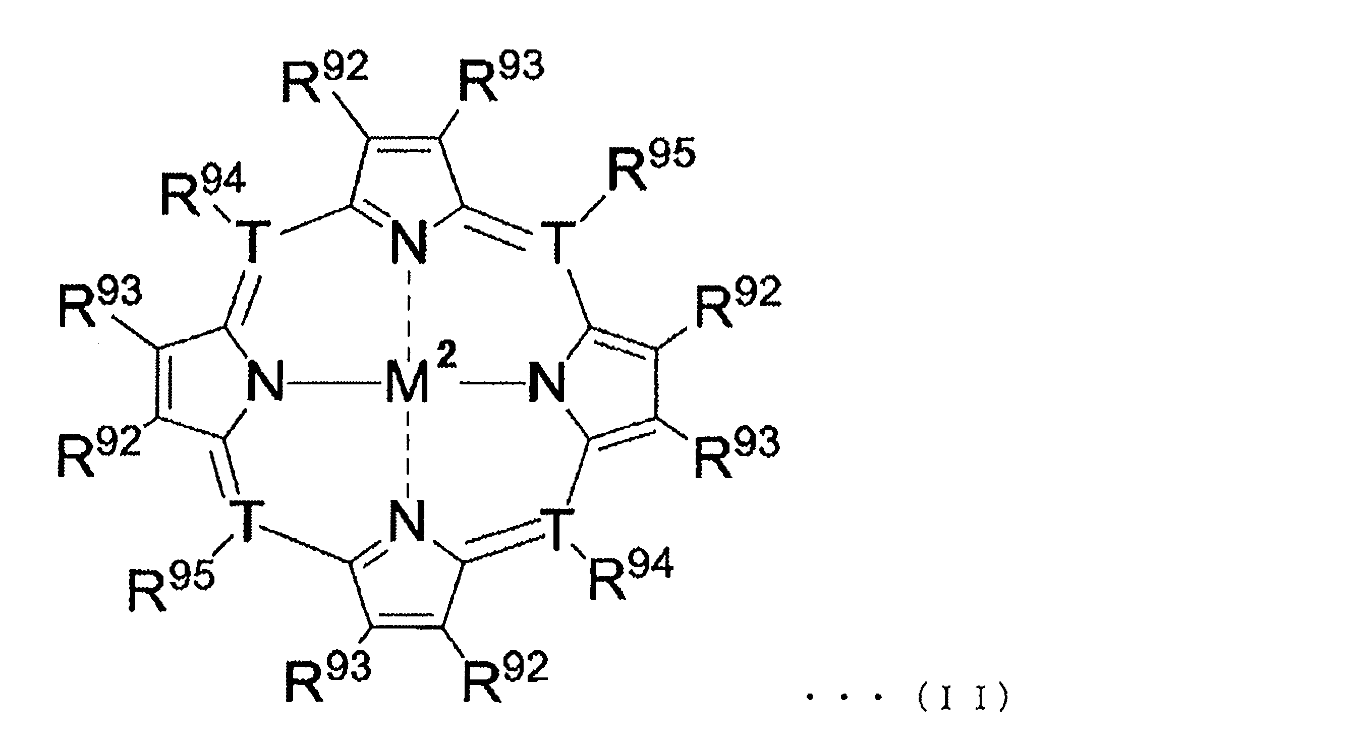
(式(II)中、M2は金属を表し、Tは炭素原子又は窒素原子を表す。R92~R95は、それぞれ独立に置換基を表す。但し、Tが窒素原子の場合は、R94及びR95は無い。)
式(I)で表される化合物について説明する。
式(I)中、Mは周期表第7~11族から選ばれる金属である。好ましくは、ルテニウム、ロジウム、パラジウム、銀、レニウム、オスミウム、イリジウム、白金、金等が挙げられる。中でもより好ましくはイリジウム又は白金である。安定性が高い点および発光効率が高い点から最も好ましくはイリジウムである。
また、式(I)中、二座配位子Lは、以下の式(III)で表される部分構造を有する配位子を示す。
式(I)中、Mは周期表第7~11族から選ばれる金属である。好ましくは、ルテニウム、ロジウム、パラジウム、銀、レニウム、オスミウム、イリジウム、白金、金等が挙げられる。中でもより好ましくはイリジウム又は白金である。安定性が高い点および発光効率が高い点から最も好ましくはイリジウムである。
また、式(I)中、二座配位子Lは、以下の式(III)で表される部分構造を有する配位子を示す。
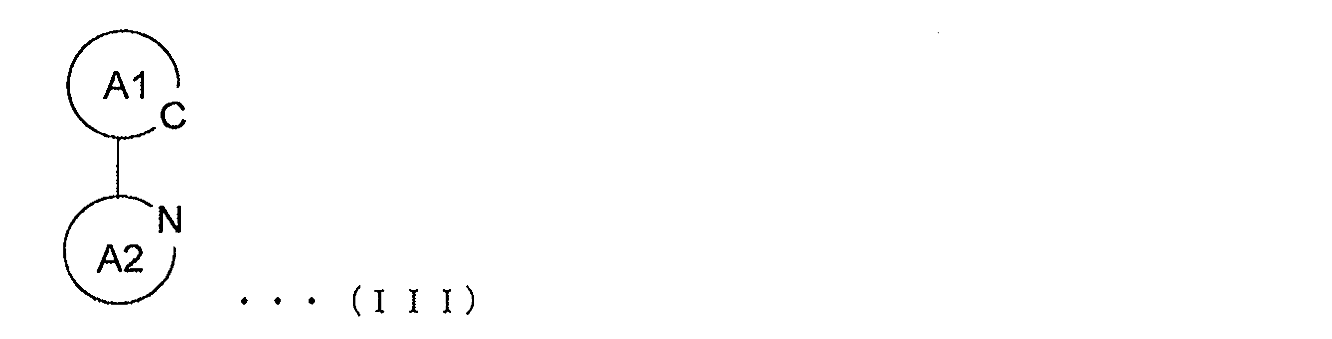
上記式(III)の部分構造において、環A1は、置換基を有していてもよい、芳香環基を表す。本発明における芳香環基は、芳香族炭化水素環基でもよいし、芳香族複素環基でもよい。
また、上記式(III)の部分構造において、環A2は、置換基を有していてもよい、含窒素芳香族複素環基を表す。
また、式(I)中、二座配位子L’は、以下の部分構造を有する配位子を示す。
また、上記式(III)の部分構造において、環A2は、置換基を有していてもよい、含窒素芳香族複素環基を表す。
また、式(I)中、二座配位子L’は、以下の部分構造を有する配位子を示す。
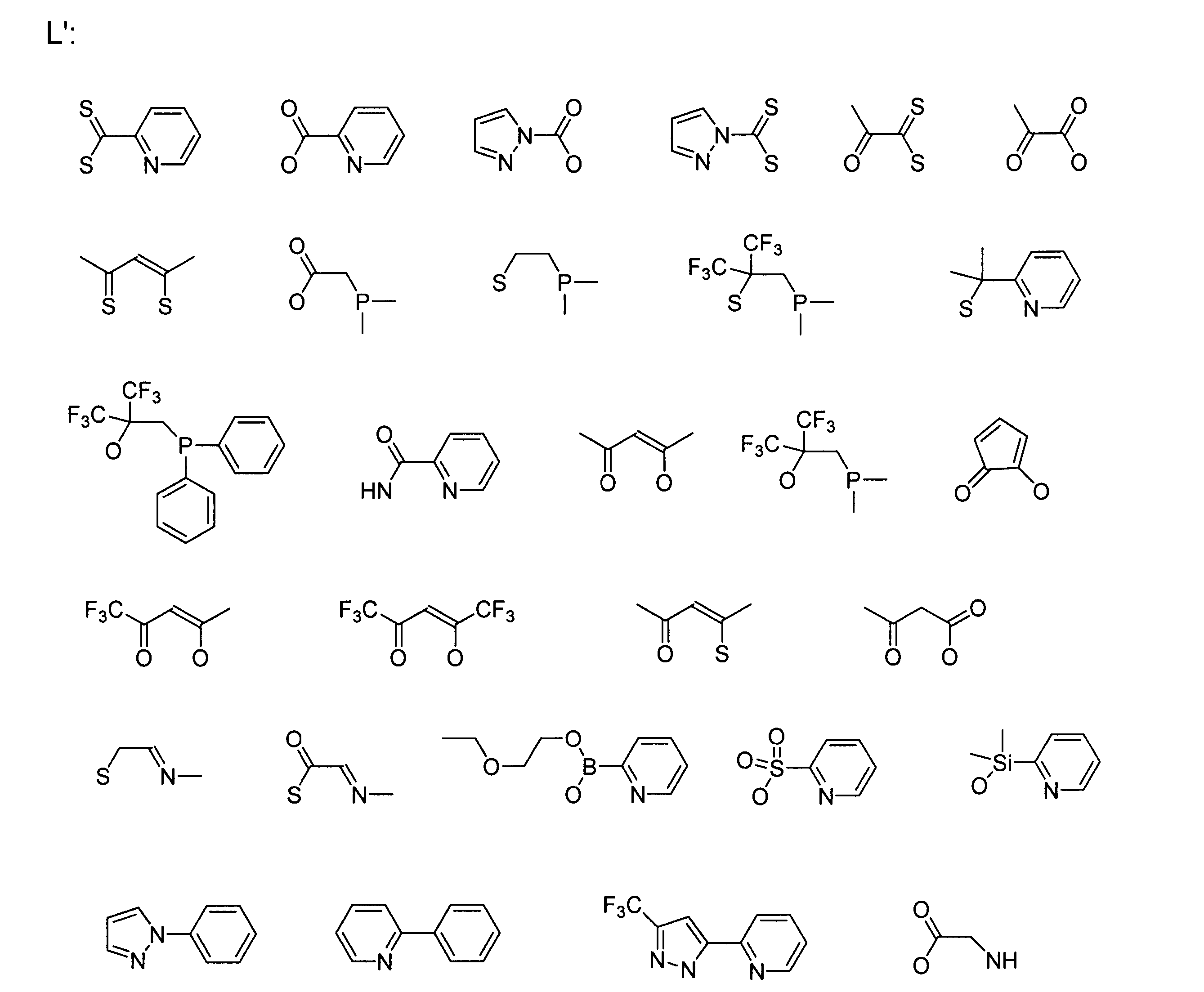
これらの中でも、L’としては、錯体の安定性の観点から以下に挙げる配位子が好ましい。
式(I)で表される化合物として、更に好ましくは、下記式(Ia)、(Ib)、(Ic)で表される化合物が挙げられる。
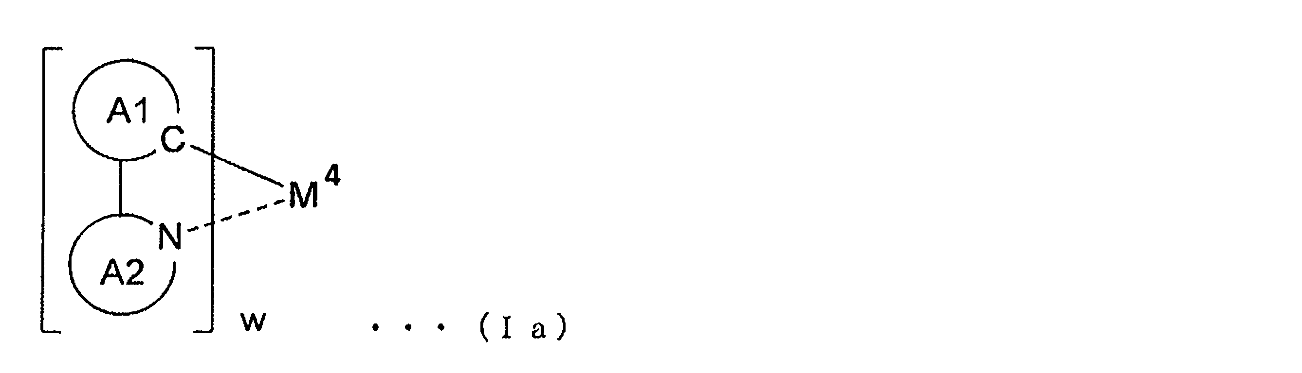
(式(Ia)中、M4は、Mと同様の金属を表し、wは、上記金属の価数を表し、環A1は、置換基を有していてもよい芳香環基を表し、環A2は、置換基を有していてもよい含窒素芳香族複素環基を表す。wが2以上で環A1および環A2が複数ある場合、複数の環A1または環A2はそれぞれ同一であっても異なってもよい。)

(式(Ib)中、M5は、Mと同様の金属を表し、w-1は、上記金属の価数を表し、環A1は、置換基を有していてもよい芳香環基を表し、環A2は、置換基を有していてもよい含窒素芳香族複素環基を表す。wが3以上で環A1および環A2が複数ある場合、複数の環A1または環A2はそれぞれ同一であっても異なってもよい。)

(式(Ic)中、M6は、Mと同様の金属を表し、wは、上記金属の価数を表し、jは、0、1又は2を表し、環A1及び環A1’は、それぞれ独立に、置換基を有していてもよい芳香環基を表し、環A2及び環A2’は、それぞれ独立に、置換基を有していてもよい含窒素芳香族複素環基を表す。w-jが2以上またはjが2以上で環A1、環A1’、環A2または環A2’が複数ある場合、複数の環A1、環A1’、環A2または環A2’はそれぞれ同一であっても異なってもよい。)
上記式(Ia)~(Ic)、(III)において、環A1及び環A1’の芳香環は、芳香族炭化水素基または芳香族複素環基である。好ましくは、2個の遊離原子価を有するベンゼン環、ナフタレン環、アントラセン環、トリフェニリル環、アセナフテン環、フルオランテン環、フルオレン環、フラン環、ベンゾフラン環、チオフェン環、ベンゾチオフェン環である。さらに好ましくはベンゼン環、ナフタレン環であり、最も好ましくはベンゼン環である。
ここで、本明細書において、遊離原子価とは、有機化学・生化学命名法(上)(改定第2版、南江堂、1992年発行)に記載のとおり、他の遊離原子価と結合を形成できるものをいう。すなわち、例えば、「1個の遊離原子価を有するベンゼン環」はフェニル基のことを言い、「2個の遊離原子価を有するベンゼン環」はフェニレン基のことを言う。
上記式(Ia)~(Ic)、(III)において、環A2及び環A2’の含窒素芳香族複素環基として、好ましくはピリジル基、ピリミジル基、ピラジニル基、トリアジニル基、イミダゾリル基、オキサゾリル基、チアゾリル基、ベンゾチアゾリル基、ベンゾオキサゾリル基、ベンゾイミダゾリル基、キノリル基、イソキノリル基、キノキサリル基、キナゾリル基、フェナントリジニル基、ベンゾチアゾール基である。
さらに好ましくはピリジル基、ピラジニル基、ピリミジル基、イミダゾリル基、キノリル基、イソキノリル基、キノキサリル基、キナゾリル基であり、特に好ましくはピリジル基、イミダゾリル基、キノリル基、イソキノリル基、キノキサリル基、キナゾリル基である。
最も好ましくはピリジル基、イミダゾリル基、キノリル基、キノキサリル基、キナゾリル基である。
上記式(Ia)~(Ic)、(III)において、環A1と環A2の組合せ構造、あるいは環A1’と環A2’の組合せ構造として最も好ましくは、置換基を有していてもよいフェニル-ピリジン構造、置換基を有していてもよいフェニル-キノリン構造、置換基を有していてもよいフェニル-キノキサリン構造、置換基を有していてもよいフェニル-イミダゾール構造、置換基を有していてもよいフェニル-キナゾリン構造である。
上記式(Ia)~(Ic)、(III)における環A1、環A1’、環A2及び環A2’が有していてもよい置換基としては、ハロゲン原子、炭素数1~12のアルキル基、炭素数1~12のアルケニル基、炭素数1~12のアルコキシカルボニル基、炭素数1~12のアルコキシ基、炭素数1~24のアラルキル基、炭素数1~12のアリールオキシ基、炭素数1~24のジアルキルアミノ基、炭素数8~24のジアリールアミノ基、5又は6員環の単環又は2~4縮合環である芳香族炭化水素環基、炭素数6~24の芳香族炭化水素基、カルバゾリル基、アシル基、ハロアルキル基、シアノ基等が挙げられる。
好ましくは、炭素数1~12のアルキル基、炭素数1~12のアルコキシ基、炭素数1~24のアラルキル基、炭素数8~24のジアリールアミノ基、5又は6員環の単環又は2~4縮合環である芳香族炭化水素環基、炭素数6~24の芳香族炭化水素基、カルバゾリル基である。
炭素数8~24のジアリールアミノ基、5又は6員環の単環又は2~4縮合環である芳香族炭化水素環基、炭素数6~24の芳香族炭化水素基、カルバゾリル基は、その基を構成するアリール部位にさらに置換基を有していてもよい。その置換基としては、炭素数1~12のアルキル基、炭素数1~12のアルコキシ基、炭素数1~24のアラルキル基、炭素数1~12のアルキル基で置換されていてもよい炭素数6~24の1価の芳香族炭化水素基が挙げられる。炭素数6~24の1価の芳香族炭化水素基としては、好ましくはベンゼン環が1ないし4連結した1価の基である。
なお、これら置換基は互いに連結して環を形成してもよい。具体例としては、環A1が有する置換基と環A2が有する置換基とが結合するか、又は、環A1’が有する置換基と環A2’が有する置換基とが結合することにより、一つの縮合環を形成してもよい。
このような縮合環としては、7,8-ベンゾキノリン基等が挙げられる。これら置換基が互いに連結して形成した環は、さらに前記置換基を有していてもよい。また、前記置換基は1つ有してもよいし、同じかまたは異なる2以上の置換基を有してもよい。
また、式(Ia)~(Ic)におけるMの好ましい例としては、式(I)におけるMと同様である。
次に、式(II)で表される化合物について説明する。
式(II)中、M2は金属を表す。具体例としては、周期表第7~11族から選ばれる金属として前述した金属が挙げられる。中でも好ましくは、ルテニウム、ロジウム、パラジウム、銀、レニウム、オスミウム、イリジウム、白金または金が挙げられ、特に好ましくは、白金、パラジウム等の2価の金属が挙げられる。
次に、式(II)で表される化合物について説明する。
式(II)中、M2は金属を表す。具体例としては、周期表第7~11族から選ばれる金属として前述した金属が挙げられる。中でも好ましくは、ルテニウム、ロジウム、パラジウム、銀、レニウム、オスミウム、イリジウム、白金または金が挙げられ、特に好ましくは、白金、パラジウム等の2価の金属が挙げられる。
また、式(II)において、R92およびR93は、それぞれ独立に、水素原子、ハロゲン原子、アルキル基、アラルキル基、アルケニル基、シアノ基、アミノ基、アシル基、アルコキシカルボニル基、カルボキシル基、アルコキシ基、アルキルアミノ基、アラルキルアミノ基、ハロアルキル基、水酸基、アリールオキシ基、芳香族炭化水素基または芳香族複素環基を表す。
更に、Tが炭素原子の場合、R94およびR95は、それぞれ独立に、R92およびR93と同様の例示物で表される置換基を表す。また、Tが窒素原子の場合は該Tに直接結合するR94またはR95は存在しない。
また、R92~R95は、更に置換基を有していてもよい。置換基としては、前記の置換基とすることができる。
更に、R92~R95のうち任意の2つ以上の基が互いに連結して環を形成してもよい。燐光発光性有機金属錯体として好ましくは式(I)で表される化合物である。
また、R92~R95は、更に置換基を有していてもよい。置換基としては、前記の置換基とすることができる。
更に、R92~R95のうち任意の2つ以上の基が互いに連結して環を形成してもよい。燐光発光性有機金属錯体として好ましくは式(I)で表される化合物である。
<フェノール性化合物>
本発明におけるフェノール性化合物は、フェノール性水酸基を有し、且つフェノール性水酸基を1位としたときに2,4,6位にはいずれか2つにのみ置換基を有するフェノール性化合物であれば特に制限はなく、3位及び/又は5位は無置換でも、置換基を有していてもよい。
本発明におけるフェノール性化合物は、フェノール性水酸基を有し、且つフェノール性水酸基を1位としたときに2,4,6位にはいずれか2つにのみ置換基を有するフェノール性化合物であれば特に制限はなく、3位及び/又は5位は無置換でも、置換基を有していてもよい。
好ましくは、この化合物は、孤立電子対を有し、電荷輸送性を有さない化合物である。より好ましくは、フェノール性水酸基を1位としたときに2,4,6位のいずれか2つにのみ置換基を有し、3位及び5位は無置換のフェノール性化合物である。
置換基は特に制限はなく、本化合物においてはフェノール構造が一つ以上存在すればよく、2つ以上のフェノール構造が存在する場合は、いずれかの構造中に本発明にて規定する構造が含まれていればよい。好ましくはフェノール性化合物中に1つのみフェノール構造が存在する。
この置換基の中でも、アルキル基、アルコキシ基、アリール基を用いたアリールオキシ基、アラルキル基が好ましい。具体的には、炭素数1~12のアルキル基、炭素数1~12のアルコキシ基、炭素数6~18のアリール基を用いたアリールオキシ基、炭素数1~24のアラルキル基から選ばれる基であることがより好ましい。
これらの中でも、アルキル基またはアルコキシ基が好ましく、炭素数1~12のアルキル基または炭素数1~12のアルコキシ基がより好ましく、特に好ましくは炭素数1~12のアルキル基である。
フェノール性水酸基を1位としたときに2,4,6位にはいずれか2つにのみ擬π共役効果を有し、孤立電子対の効果、すなわち孤立電子対が安定化する効果を弱める力を持つと考えられる。孤立電子対が安定化するとフェノール性水酸基からのプロトンが脱離しやすくなり、脱離したプロトンによる悪影響が懸念されるが、孤立電子対の安定化効果を弱めることで、プロトンが脱離しにくくなり、好ましい。
これらの位置に置換基を有することでフェノール性化合物の安定性が向上する。さらに、置換基がアルキル基またはアルコキシ基の様な電子供与性基の場合は、酸素原子の孤立電子対の電子密度が増大し、正孔を閉じ込める効果が向上すると考えられる。
フェノール構造は共鳴効果により、負電荷が酸素原子上およびフェノール性水酸基を1位としたときの2,4,6位に非局在化する。負電荷が局在化した位置は反応性が高いため、通常よく用いられる酸化防止剤であるBHTは、2,4,6位に有するアルキル基によって、フェノール性化合物自体の安定性も向上している。
ところが驚くべきことに、燐光発光材料および電荷輸送性化合物を含む有機電界発光素子の発光層に用いるフェノール性化合物の場合は、フェノール性水酸基を1位としたときの2,4,6位にはいずれか2つにのみ置換基を有し、あえて負電荷密度が高く反応性に富むと考えられる位置の一つに置換基を有さない化合物を用いることにより、有機電界発光素子の効率が向上し、駆動安定性が向上することが見出された。
この理由は、酸素原子以外に、負電荷密度の高い位置が一つ存在することによって、正孔を閉じ込める効果が向上しているためと考えられる。そのため、フェノール性水酸基を1位としたときの2,4,6位の置換基の数は3つではなく、2つであることが必要である。
さらに好ましくは、フェノール性化合物は、フェノール性水酸基を1位としたときの2,4,6位のいずれか2つのみに置換基を有することである。この理由は、フェノール性水酸基を1位としたときの2,4,6位のいずれか2つにのみ置換基を有することで、電荷のホッピング輸送が阻害されにくいためであると考えられる。
さらに、フェノール性水酸基を1位としたときの2,4,6位のうち、2,6位の2つにのみ置換基を有する場合、水酸基の酸素原子の孤立電子対が保護されてフェノール性化合物が最も安定となるため、有機電界発光素子の効率を向上させるとともに駆動安定性も向上すると考えられ、特に好ましい。
また、置換基がアルコキシ基である場合、フェノール性水酸基を1位としたときの2,4,6位のいずれか2つのみに置換基を有することで、フェノール性水酸基の酸素原子及びアルコキシ基の酸素原子の電子密度が適度に増大し、正孔を閉じ込める効果を向上させつつ安定性にも優れた状態が維持されると考えられる。
また具体的な構造式として本発明におけるフェノール性化合物は下記式(1)にて表すこともできる。ただし、本化合物は下記構造式に限定されるものではない。

ただし、Aは置換基を有するフェノール構造である。nは1~5の整数である。好ましくは、Lはn=1の場合は存在せず、n=2~5の場合は連結基である。nが2~5の場合、Aが有する置換基は同じであっても異なっていてもよい。
Aは、n=1の場合、フェノール構造の水酸基を1位とした場合、2、4、6位にはいずれか2ヶ所にのみ置換基を有し、また3位または5位に置換基を有していてもよい。
Aが有していてもよい置換基は、炭素数1~12のアルキル基、炭素数1~12のアルコキシ基、炭素数6~18のアリール基を用いたアリールオキシ基、炭素数1~24のアラルキル基である。
好ましくは、化合物の安定性の観点からフェノール構造の水酸基を1位とした場合の2位又は6位はアルキル基である。更に2位および6位に置換されるアルキル基は、発光層形成用組成物中の他の材料と干渉することを避けるため、立体障害を有する2級アルキル基(イソプロピル基など)または3級アルキル基(tert―ブチル基など)であるアルキル基が好ましく、立体障害性が最も高い3級アルキル基が最も好ましい。
n=2~5の場合、Aは連結基Lを有する。Lは、Aに対して、sp3混成軌道を有する炭素または酸素で結合する。Lは、2~6位のいずれに置換してもよいが、2,4,6位に置換する場合には、化合物Aの置換基の規定である「2,4,6位にはいずれか2ヶ所にのみ置換基を有する」に該当する。
すなわち、骨格Aの2,4,6位にはいずれか2ヶ所にのみ、連結基とそれ以外の置換基1種が置換する。nは特に限定されるものではないが、好ましくは、3以下、更に好ましくは2以下であり、最も好ましいのは1である。発光層形成後に均一に広がり、フェノール性水酸基濃度が均一に広がるため、電荷トラップが均一に発生し、電荷再結合が膜内に均一におこることで励起子の濃度消光を防止すると推定されるためである。
Lは、sp3混成軌道を有する炭素または酸素で結合するのであれば、特に限定されるものではない。好ましくは、炭素1~12のアルキル基の置換基を有してもよいアルキレンである。共役鎖を有する場合、上記アルキル基の炭素数は2~6であることが好ましい。理由としては、発光材料と共存させる場合において、消光因子と成り得る要素の排除、すなわち共役鎖の拡大によるエネルギー移動型の消光を防止するためである。
具体的な構造としては、2,6-tert-ブチルフェノール、4-メトキシ-2-tert-ブチルフェノール、4,4’-ブチリデンビス(6-t-ブチル-3-メチルフェノール)など、下記に記載された化合物が挙げられる。
<電荷輸送性化合物>
本発明の組成物が含有し得る電荷輸送性化合物としては、従来有機電界発光素子用材料として用いられているものを使用することができる。例えば、ピリジン、カルバゾール、ナフタレン、ペリレン、ピレン、アントラセン、クリセン、ナフタセン、フェナントレン、コロネン、フルオランテン、ベンゾフェナントレン、フルオレン、アセトナフトフルオランテン、クマリン、p-ビス(2-フェニルエテニル)ベンゼンおよびそれらの誘導体、キナクリドン誘導体、DCM(4-(dicyanomethylene)-2-methyl-6-(p-dimethylaminostyryl)-4H-pyran)系化合物、ベンゾピラン誘導体、ローダミン誘導体、ベンゾチオキサンテン誘導体、アザベンゾチオキサンテン、アリールアミノ基が置換された縮合芳香族環化合物、アリールアミノ基が置換されたスチリル誘導体等が挙げられる。
これらは1種類を単独で用いてもよく、また2種類以上を任意の組み合わせ、および比率で用いてもよい。
本発明の組成物が含有し得る電荷輸送性化合物としては、従来有機電界発光素子用材料として用いられているものを使用することができる。例えば、ピリジン、カルバゾール、ナフタレン、ペリレン、ピレン、アントラセン、クリセン、ナフタセン、フェナントレン、コロネン、フルオランテン、ベンゾフェナントレン、フルオレン、アセトナフトフルオランテン、クマリン、p-ビス(2-フェニルエテニル)ベンゼンおよびそれらの誘導体、キナクリドン誘導体、DCM(4-(dicyanomethylene)-2-methyl-6-(p-dimethylaminostyryl)-4H-pyran)系化合物、ベンゾピラン誘導体、ローダミン誘導体、ベンゾチオキサンテン誘導体、アザベンゾチオキサンテン、アリールアミノ基が置換された縮合芳香族環化合物、アリールアミノ基が置換されたスチリル誘導体等が挙げられる。
これらは1種類を単独で用いてもよく、また2種類以上を任意の組み合わせ、および比率で用いてもよい。
本発明の組成物における電荷輸送性化合物の含有量は、通常0.01質量%以上、好ましくは0.1質量%以上である。また、本発明の組成物における電荷輸送性化合物の含有量は、通常50質量%以下、好ましくは30質量%以下、さらに好ましくは10質量%以下である。
<発光層形成用組成物>
本発明の組成物は、少なくとも燐光発光材料、電荷輸送性化合物、前記フェノール性化合物を含有する。また、インク等の組成物には溶媒を含有してもよい。本発明の組成物は通常湿式成膜法で層や膜を形成するために用いられ、特に有機電界発光素子の発光層を形成するために用いられることが好ましい。
すなわち、本発明の組成物は、有機電界発光素子用組成物であることが好ましく、更に有機電界発光素子の発光層形成用組成物として用いられることが特に好ましい。
本発明の組成物は、少なくとも燐光発光材料、電荷輸送性化合物、前記フェノール性化合物を含有する。また、インク等の組成物には溶媒を含有してもよい。本発明の組成物は通常湿式成膜法で層や膜を形成するために用いられ、特に有機電界発光素子の発光層を形成するために用いられることが好ましい。
すなわち、本発明の組成物は、有機電界発光素子用組成物であることが好ましく、更に有機電界発光素子の発光層形成用組成物として用いられることが特に好ましい。
本発明の組成物における燐光発光材料の含有量は、電荷輸送性化合物の総量に対して、通常1質量%以上、好ましくは5質量%以上、更に好ましくは15質量%以上である。また、本発明の組成物における燐光発光材料の含有量は、電荷輸送性化合物の総量に対して、通常50質量%以下、好ましくは40質量%以下である。
組成物中の燐光発光材料の含有量を上記範囲とすることにより、例えば、この組成物を用いて発光層を形成した場合、隣接する層(例えば、正孔輸送層や正孔阻止層)から発光層へ効率よく、正孔や電子の注入が行われ、駆動電圧を低減することができる。尚、燐光発光材料は組成物中に、1種のみ含まれていてもよく、2種以上が組み合わされて含まれていてもよい。
また、発光材料の発光色は、特に限定されるものではないが、長波長であるほうが好ましい。具体的には、該組成物の塗布膜の発光の色(ピーク波長)が、緑色よりも長波(500nm以上)、更に好ましくは黄緑色よりも長波(550nm以上)であることが好ましい。
燐光発光層の発光原理から、孤立電子対による3重項励起状態の消光がおこるが、長波長発光の励起状態の方が、短波長発光の励起状態に比べ、エネルギーが低く、3重項励起状態自身が安定であり、そのため孤立電子対による消光の影響を受けにくいと推測される。
本発明の組成物における溶媒に対するフェノール性化合物の含有量は、組成物中の電荷輸送性化合物の総量に対して、通常0.01質量%以上であり、好ましくは0.1質量%以上である。また、組成物中の電荷輸送性化合物の総量に対して、通常10質量%以下、より好ましくは5質量%以下、更に好ましくは、1質量%以下である。
下限以上であれば、電荷の捕捉による効率の向上がおこるためである。また、過剰に含有される場合は、組成物を用いて膜を形成した際に、2,6位の立体障害を超えた孤立電子対の相互作用の発現による消光の可能性が予測されるためである。
<その他の成分>
本発明の組成物を例えば有機電界発光素子用に用いる場合、組成物には、上述の燐光発光材料、フェノール性水酸基を有する化合物および電荷輸送性化合物の他、インクに用いる際には溶媒を含有することができる。
本発明の組成物に含有してもよい溶媒は、湿式成膜により金属錯体化合物を含む層を形成するために用いる、揮発性を有する液体成分である。
本発明の組成物を例えば有機電界発光素子用に用いる場合、組成物には、上述の燐光発光材料、フェノール性水酸基を有する化合物および電荷輸送性化合物の他、インクに用いる際には溶媒を含有することができる。
本発明の組成物に含有してもよい溶媒は、湿式成膜により金属錯体化合物を含む層を形成するために用いる、揮発性を有する液体成分である。
該溶媒は、溶質である金属錯体化合物、後述の電荷輸送性化合物、および本発明のフェノール性化合物が良好に溶解する溶媒であれば特に限定されない。
好ましい溶媒としては、例えば、n-デカン、シクロヘキサン、エチルシクロヘキサン、デカリン、ビシクロヘキサン等のアルカン類;トルエン、キシレン、メシチレン、フェニルシクロヘキサン、テトラリン等の芳香族炭化水素類;クロロベンゼン、ジクロロベンゼン、トリクロロベンゼン等のハロゲン化芳香族炭化水素類;1,2-ジメトキシベンゼン、1,3-ジメトキシベンゼン、アニソール、フェネトール、2-メトキシトルエン、3-メトキシトルエン、4-メトキシトルエン、2,3-ジメチルアニソール、2,4-ジメチルアニソール、ジフェニルエーテル等の芳香族エーテル類;酢酸フェニル、プロピオン酸フェニル、安息香酸メチル、安息香酸エチル、安息香酸プロピル、安息香酸n-ブチル等の芳香族エステル類、シクロヘキサノン、シクロオクタノン、フェンコン等の脂環族ケトン類;シクロヘキサノール、シクロオクタノール等の脂環族アルコール類;メチルエチルケトン、ジブチルケトン等の脂肪族ケトン類;ブタノール、ヘキサノール等の脂肪族アルコール類;エチレングリコールジメチルエーテル、エチレングリコールジエチルエーテル、プロピレングリコール-1-モノメチルエーテルアセタート(PGMEA)等の脂肪族エーテル類;等が挙げられる。
中でも好ましくは、アルカン類や芳香族炭化水素類であり、特に、フェニルシクロヘキサンは湿式成膜プロセスにおいて好ましい粘度と沸点を有している。
これらの溶媒は1種類を単独で用いてもよく、また2種類以上を任意の組み合わせ、および比率で用いてもよい。
溶媒の沸点は、通常80℃以上、好ましくは90℃以上、より好ましくは100℃以上、特に好ましくは110℃以上である。また、溶媒の沸点は、通常300℃以下、好ましくは280℃以下、より好ましくは250℃以下である。溶媒の沸点が上記下限を下回ると、湿式成膜時において、組成物からの溶媒蒸発により、成膜安定性が低下する可能性がある。
本発明の組成物における溶媒の含有量は、通常10質量%以上、好ましくは20質量%以上、より好ましくは50質量%以上、さらに好ましくは80質量%以上である。また、本発明の組成物における溶媒の含有量は、通常99.99質量%以下、好ましくは99.95質量%以下、より好ましくは99.9質量%以下、さらに好ましくは99.8質量%以下である。
例えば、発光層は通常3~200nm程度の厚みに形成されるが、本発明の組成物を用いてこのような厚みの発光層を形成する場合、溶媒の含有量が上記下限を下回ると、組成物の粘性が高くなりすぎ、成膜作業性が低下する可能性がある。一方、上記上限を上回ると、成膜後、溶媒を除去して得られる膜の厚みが稼げなくなるため、成膜が困難となる傾向がある。
本発明の組成物には、必要に応じて、上記の化合物等の他に、更に他の化合物等を含有していてもよい。例えば、上記の溶媒の他に、別の溶媒を含有していてもよい。そのような溶媒としては、例えば、N,N-ジメチルホルムアミド、N,N-ジメチルアセトアミド等のアミド類、ジメチルスルホキシド等が挙げられる。これらは1種類を単独で用いてもよく、また2種類以上を任意の組み合わせ、および比率で用いてもよい。
<湿式成膜法>
湿式成膜法とは、基板上に、溶媒を含む組成物を塗布し、溶媒を乾燥除去して膜を形成する方法をいう。塗布方法としては、特に限定はされないが、例えばスピンコート法、ディップコート法、ダイコート法、バーコート法、ブレードコート法、ロールコート法、スプレーコート法、キャピラリーコート法、インクジェット法、スクリーン印刷法、グラビア印刷法、フレキソ印刷法等が挙げられる。
湿式成膜法とは、基板上に、溶媒を含む組成物を塗布し、溶媒を乾燥除去して膜を形成する方法をいう。塗布方法としては、特に限定はされないが、例えばスピンコート法、ディップコート法、ダイコート法、バーコート法、ブレードコート法、ロールコート法、スプレーコート法、キャピラリーコート法、インクジェット法、スクリーン印刷法、グラビア印刷法、フレキソ印刷法等が挙げられる。
溶媒を乾燥除去する方法としては、通常、加熱乾燥を行う。加熱工程において使用する加熱手段の例としては、クリーンオーブン、ホットプレート、赤外線加熱が挙げられる。赤外線加熱としては、ハロゲンヒーターやセラミックコートしたハロゲンヒーター、セラミックヒーター等が使用できる。
赤外線による加熱は基板あるいは膜に直接熱エネルギーを与えるため、オーブンやホットプレートを用いた加熱と比べて短時間での乾燥が可能となる。そのため加熱雰囲気のガス(水分や酸素)の影響や、微小なごみの影響を最小限に抑えることができ、生産性が向上し、好ましい。
加熱温度は、通常70℃以上、好ましくは75℃以上、より好ましくは80℃以上である。また、加熱温度は、通常150℃以下、好ましくは、140℃以下、より好ましくは、130℃以下である。
加熱時間は、通常10秒以上、好ましくは60秒以上、より好ましくは90秒以上であり、通常120分以下、好ましくは60分以下、より好ましくは30分以下である。
また、加熱乾燥の前に真空乾燥を行うことも好ましい。
本発明の組成物を湿式成膜法にて成膜した有機層の膜厚は、通常5nm以上、好ましくは10nm以上、さらに好ましくは20nm以上である。また、膜厚は、通常500nm以下、好ましくは300nm以下、さらに好ましくは200nm以下である。
本発明の組成物を湿式成膜法にて成膜した有機層の膜厚は、通常5nm以上、好ましくは10nm以上、さらに好ましくは20nm以上である。また、膜厚は、通常500nm以下、好ましくは300nm以下、さらに好ましくは200nm以下である。
[有機電界発光素子]
本発明に係る有機電界発光素子は、陽極、陰極、及びこれらの間に少なくとも1層の有機層を有する有機電界発光素子であって、該有機層のうち少なくとも1層が、本発明の組成物を用いて湿式製膜により形成された層であることを特徴とする。この層は発光層であることが好ましい。
本発明に係る有機電界発光素子は、陽極、陰極、及びこれらの間に少なくとも1層の有機層を有する有機電界発光素子であって、該有機層のうち少なくとも1層が、本発明の組成物を用いて湿式製膜により形成された層であることを特徴とする。この層は発光層であることが好ましい。
図1は本発明にかかる有機電界発光素子に好適な構造例を示す断面の模式図であり、図1において、符号1は基板、符号2は陽極、符号3は正孔注入層、符号4は正孔輸送層、符号5は発光層、符号6は正孔阻止層、符号7は電子輸送層、符号8は電子注入層、符号9は陰極を各々表す。
[1]基板
基板1は有機電界発光素子の支持体となるものであり、石英やガラスの板、金属板や金属箔、プラスチックフィルムやシートなどが用いられる。特にガラス板や、ポリエステル、ポリメタクリレート、ポリカーボネート、ポリスルホンなどの透明な合成樹脂の板が好ましい。
基板1は有機電界発光素子の支持体となるものであり、石英やガラスの板、金属板や金属箔、プラスチックフィルムやシートなどが用いられる。特にガラス板や、ポリエステル、ポリメタクリレート、ポリカーボネート、ポリスルホンなどの透明な合成樹脂の板が好ましい。
合成樹脂基板を使用する場合にはガスバリア性に留意する必要がある。基板のガスバリア性が小さすぎると、基板を通過した外気により有機電界発光素子が劣化することがあるので好ましくない。このため、合成樹脂基板の少なくとも片面に緻密なシリコン酸化膜等を設けてガスバリア性を確保する方法も好ましい方法の一つである。
[2]陽極
基板1上には陽極2が設けられる。陽極2は発光層側の層(正孔注入層3、正孔輸送層4又は発光層5など)への正孔注入の役割を果たすものである。
基板1上には陽極2が設けられる。陽極2は発光層側の層(正孔注入層3、正孔輸送層4又は発光層5など)への正孔注入の役割を果たすものである。
この陽極2は、通常、アルミニウム、金、銀、ニッケル、パラジウム、白金等の金属、インジウム及び/又はスズの酸化物などの金属酸化物、ヨウ化銅などのハロゲン化金属、カーボンブラック、あるいは、ポリ(3-メチルチオフェン)、ポリピロール、ポリアニリン等の導電性高分子などにより構成される。
陽極2の形成は通常、スパッタリング法、真空蒸着法などにより行うことができる。また、銀などの金属微粒子、ヨウ化銅などの微粒子、カーボンブラック、導電性の金属酸化物微粒子、導電性高分子微粉末などを用いて陽極を形成する場合には、適当なバインダー樹脂溶液に分散させて、基板1上に塗布することにより陽極2を形成することもできる。さらに、導電性高分子の場合は、電解重合により直接基板1上に薄膜を形成したり、基板1上に導電性高分子を塗布して陽極2を形成することもできる(Appl.Phys.Lett.,60巻,2711頁,1992年)。
陽極2は通常は単層構造であるが、所望により複数の材料からなる積層構造とすることも可能である。
陽極2の厚みは、必要とする透明性により異なる。透明性が必要とされる場合は、可視光の透過率を、通常60%以上、好ましくは80%以上とする。この場合、陽極の厚みは通常5nm以上、好ましくは10nm以上である。また、この場合、陽極の厚みは通常1000nm以下、好ましくは500nm以下程度である。不透明でよい場合は陽極2の厚みは任意であり、陽極2は基板1と同一でもよい。また、さらには上記の陽極2の上に異なる導電材料を積層することも可能である。
陽極に付着した不純物を除去し、イオン化ポテンシャルを調整して正孔注入性を向上させることを目的に、陽極表面を紫外線(UV)/オゾン処理をしたり、酸素プラズマ処理や、アルゴンプラズマ処理をすることが好ましい。
陽極2の厚みは、必要とする透明性により異なる。透明性が必要とされる場合は、可視光の透過率を、通常60%以上、好ましくは80%以上とする。この場合、陽極の厚みは通常5nm以上、好ましくは10nm以上である。また、この場合、陽極の厚みは通常1000nm以下、好ましくは500nm以下程度である。不透明でよい場合は陽極2の厚みは任意であり、陽極2は基板1と同一でもよい。また、さらには上記の陽極2の上に異なる導電材料を積層することも可能である。
陽極に付着した不純物を除去し、イオン化ポテンシャルを調整して正孔注入性を向上させることを目的に、陽極表面を紫外線(UV)/オゾン処理をしたり、酸素プラズマ処理や、アルゴンプラズマ処理をすることが好ましい。
[3]正孔注入層
正孔注入層3は、陽極2から発光層5へ正孔を輸送する層であり、通常、陽極2上に形成することができる。
本発明に係る正孔注入層3の形成方法は真空蒸着法でも、湿式成膜法でもよく、特に制限はないが、ダークスポット低減の観点から正孔注入層3を湿式成膜法により形成することが好ましい。
正孔注入層3の膜厚は、通常5nm以上、好ましくは10nm以上である。また、正孔注入層3の膜厚は、通常1000nm以下、好ましくは500nm以下の範囲である。
正孔注入層3は、陽極2から発光層5へ正孔を輸送する層であり、通常、陽極2上に形成することができる。
本発明に係る正孔注入層3の形成方法は真空蒸着法でも、湿式成膜法でもよく、特に制限はないが、ダークスポット低減の観点から正孔注入層3を湿式成膜法により形成することが好ましい。
正孔注入層3の膜厚は、通常5nm以上、好ましくは10nm以上である。また、正孔注入層3の膜厚は、通常1000nm以下、好ましくは500nm以下の範囲である。
<湿式成膜法による正孔注入層の形成>
湿式成膜により正孔注入層3を形成する場合、通常は、正孔注入層3を構成する材料を適切な溶媒(正孔注入層用溶媒)と混合して塗布用の組成物(正孔注入層形成用組成物)を調製し、この正孔注入層形成用組成物を適切な手法により、正孔注入層3の下層に該当する層(通常は、陽極)上に塗布し、乾燥することにより正孔注入層3を形成する。
湿式成膜により正孔注入層3を形成する場合、通常は、正孔注入層3を構成する材料を適切な溶媒(正孔注入層用溶媒)と混合して塗布用の組成物(正孔注入層形成用組成物)を調製し、この正孔注入層形成用組成物を適切な手法により、正孔注入層3の下層に該当する層(通常は、陽極)上に塗布し、乾燥することにより正孔注入層3を形成する。
(正孔輸送性化合物)
正孔注入層形成用組成物は通常、正孔注入層の構成材料として正孔輸送性化合物及び溶媒を含有する。正孔輸送性化合物は、通常、有機電界発光素子の正孔注入層に使用される、正孔輸送性を有する化合物であれば、重合体などの高分子化合物であっても、単量体などの低分子化合物であってもよいが、高分子化合物であることが好ましい。
正孔注入層形成用組成物は通常、正孔注入層の構成材料として正孔輸送性化合物及び溶媒を含有する。正孔輸送性化合物は、通常、有機電界発光素子の正孔注入層に使用される、正孔輸送性を有する化合物であれば、重合体などの高分子化合物であっても、単量体などの低分子化合物であってもよいが、高分子化合物であることが好ましい。
正孔輸送性化合物としては、陽極2から正孔注入層3への電荷注入障壁の観点から4.5eV~6.0eVのイオン化ポテンシャルを有する化合物が好ましい。
正孔輸送性化合物の例としては、芳香族アミン誘導体、フタロシアニン誘導体、ポルフィリン誘導体、オリゴチオフェン誘導体、ポリチオフェン誘導体、ベンジルフェニル誘導体、フルオレン基で3級アミンを連結した化合物、ヒドラゾン誘導体、シラザン誘導体、シラナミン誘導体、ホスファミン誘導体、キナクリドン誘導体、ポリアニリン誘導体、ポリピロール誘導体、ポリフェニレンビニレン誘導体、ポリチエニレンビニレン誘導体、ポリキノリン誘導体、ポリキノキサリン誘導体、カーボン等が挙げられる。
尚、本明細書において誘導体とは、例えば、芳香族アミン誘導体を例にするならば、芳香族アミンそのもの及び芳香族アミンを主骨格とする化合物を含むものであり、重合体であっても、単量体であってもよい。
上記例示した中でも非晶質性、可視光の透過率の点から、芳香族アミン化合物が好ましく、特に芳香族三級アミン化合物が好ましい。ここで、芳香族三級アミン化合物とは、芳香族三級アミン構造を有する化合物であって、芳香族三級アミン由来の基を有する化合物も含む。
芳香族三級アミン化合物の種類は特に制限されないが、表面平滑化効果による均一な発光の点から、重量平均分子量が1000以上、1000000以下の高分子化合物(繰り返し単位が連なる重合型化合物)がさらに好ましい。
このような高分子化合物の材料としては、従来、正孔注入層用化合物として用いられている化合物を用いることができ、例えば、日本国特開2009-212510号公報、国際公開第2012/096352号、国際公開第2013/191137号等に開示されている化合物を用いることができる。
また、正孔輸送性化合物としては、ポリチオフェンの誘導体である3,4-ethylenedioxythiophene(3,4-エチレンジオキシチオフェン)を高分子量ポリスチレンスルホン酸中で重合してなる導電性ポリマー(PEDOT/PSS)もまた好ましい。また、このポリマーの末端をメタクリレート等でキャップしたものであってもよい。
正孔注入層形成用組成物中の正孔輸送性化合物の濃度は、本発明の効果を著しく損なわない限り任意であるが、膜厚の均一性の点で通常0.01質量%以上、好ましくは0.1質量%以上、さらに好ましくは0.5質量%以上である。また、正孔注入層形成用組成物中の正孔輸送性化合物の濃度は、通常70質量%以下、好ましくは60質量%以下、さらに好ましくは50質量%以下である。この濃度が高すぎると膜厚にムラが生じる可能性があり、また、低すぎると成膜された正孔注入層に欠陥が生じる可能性がある。
(電子受容性化合物)
正孔注入層形成用組成物は正孔注入層の構成材料として、電子受容性化合物を含有していることが好ましい。
電子受容性化合物とは、酸化力を有し、上述の正孔輸送性化合物から一電子受容する能力を有する化合物が好ましく、具体的には、電子親和力が4eV以上である化合物が好ましく、5eV以上である化合物がさらに好ましい。
正孔注入層形成用組成物は正孔注入層の構成材料として、電子受容性化合物を含有していることが好ましい。
電子受容性化合物とは、酸化力を有し、上述の正孔輸送性化合物から一電子受容する能力を有する化合物が好ましく、具体的には、電子親和力が4eV以上である化合物が好ましく、5eV以上である化合物がさらに好ましい。
このような電子受容性化合物としては、例えば、トリアリールホウ素化合物、ハロゲン化金属、ルイス酸、有機酸、オニウム塩、アリールアミンとハロゲン化金属との塩、アリールアミンとルイス酸との塩よりなる群から選ばれる1種又は2種以上の化合物等が挙げられる。
さらに具体的には、塩化鉄(III)(日本国特開平11-251067号公報)、ペルオキソ二硫酸アンモニウム等の高原子価の無機化合物;テトラシアノエチレン等のシアノ化合物、トリス(ペンタフルオロフェニル)ボラン(日本国特開2003-31365号公報)等の芳香族ホウ素化合物;有機基の置換したオニウム塩(国際公開第2005/089024号);フラーレン誘導体;ヨウ素;ポリスチレンスルホン酸イオン、アルキルベンゼンスルホン酸イオン、ショウノウスルホン酸イオン等のスルホン酸イオン等が挙げられる。
これらの電子受容性化合物は、正孔輸送性化合物を酸化することにより正孔注入層の導電率を向上させることができる。
正孔注入層あるいは正孔注入層形成用組成物中の電子受容性化合物の正孔輸送性化合物に対する含有量は、通常0.1モル%以上、好ましくは1モル%以上である。但し、通常100モル%以下、好ましくは40モル%以下である。
正孔注入層あるいは正孔注入層形成用組成物中の電子受容性化合物の正孔輸送性化合物に対する含有量は、通常0.1モル%以上、好ましくは1モル%以上である。但し、通常100モル%以下、好ましくは40モル%以下である。
(溶媒)
湿式成膜法に用いる正孔注入層形成用組成物の溶媒のうち少なくとも1種は、上述の正孔注入層の構成材料を溶解しうる化合物であることが好ましい。また、この溶媒の沸点は通常80℃以上、好ましくは100℃以上、さらに好ましくは110℃以上である。溶媒の沸点は通常300℃以下、好ましくは280℃以下であることが好ましい。
湿式成膜法に用いる正孔注入層形成用組成物の溶媒のうち少なくとも1種は、上述の正孔注入層の構成材料を溶解しうる化合物であることが好ましい。また、この溶媒の沸点は通常80℃以上、好ましくは100℃以上、さらに好ましくは110℃以上である。溶媒の沸点は通常300℃以下、好ましくは280℃以下であることが好ましい。
溶媒の沸点が低すぎると、乾燥速度が速すぎ、膜質が悪化する可能性がある。また、溶媒の沸点が高すぎると乾燥工程の温度を高くする必要があり、他の層や基板に悪影響を与える可能性がある。
溶媒として例えば、エーテル系溶媒、エステル系溶媒、芳香族炭化水素系溶媒、アミド系溶媒などが挙げられる。
エーテル系溶媒としては、例えば、エチレングリコールジメチルエーテル、エチレングリコールジエチルエーテル、プロピレングリコール-1-モノメチルエーテルアセタート(PGMEA)等の脂肪族エーテル;1,2-ジメトキシベンゼン、1,3-ジメトキシベンゼン、アニソール、フェネトール、2-メトキシトルエン、3-メトキシトルエン、4-メトキシトルエン、2,3-ジメチルアニソール、2,4-ジメチルアニソール等の芳香族エーテル、等が挙げられる。
エステル系溶媒としては、例えば、酢酸フェニル、プロピオン酸フェニル、安息香酸メチル、安息香酸エチル、安息香酸プロピル、安息香酸n-ブチル等の芳香族エステル、等が挙げられる。
芳香族炭化水素系溶媒としては、例えば、トルエン、キシレン、シクロヘキシルベンゼン、3-イソプロピルビフェニル、1,2,3,4-テトラメチルベンゼン、1,4-ジイソプロピルベンゼン、メチルナフタレン等が挙げられる。
アミド系溶媒としては、例えば、N,N-ジメチルホルムアミド、N,N-ジメチルアセトアミド、等が挙げられる。
その他、ジメチルスルホキシド等も用いることができる。
これらの溶媒は1種のみを用いてもよく、2種以上を任意の組み合わせ及び比率で用いてもよい。
その他、ジメチルスルホキシド等も用いることができる。
これらの溶媒は1種のみを用いてもよく、2種以上を任意の組み合わせ及び比率で用いてもよい。
(成膜方法)
正孔注入層形成用組成物を調製後、この組成物を湿式成膜により、正孔注入層3の下層に該当する層(通常は、陽極2)上に塗布し、乾燥することにより正孔注入層3を形成する。
塗布工程における温度は、組成物中に結晶が生じることによる膜の欠損を防ぐため、10℃以上が好ましく、50℃以下が好ましい。
正孔注入層形成用組成物を調製後、この組成物を湿式成膜により、正孔注入層3の下層に該当する層(通常は、陽極2)上に塗布し、乾燥することにより正孔注入層3を形成する。
塗布工程における温度は、組成物中に結晶が生じることによる膜の欠損を防ぐため、10℃以上が好ましく、50℃以下が好ましい。
塗布工程における相対湿度は、本発明の効果を著しく損なわない限り限定されないが、通常0.01ppm以上、通常80%以下である。
塗布後、必要に応じて、真空乾燥などにより大雑把に溶媒を除去し、その後加熱により正孔注入層形成用組成物の膜を乾燥する。加熱工程において使用する加熱手段の例を挙げると、クリーンオーブン、ホットプレート、赤外線ヒーター(ハロゲンヒーター)などが挙げられる。
塗布後、必要に応じて、真空乾燥などにより大雑把に溶媒を除去し、その後加熱により正孔注入層形成用組成物の膜を乾燥する。加熱工程において使用する加熱手段の例を挙げると、クリーンオーブン、ホットプレート、赤外線ヒーター(ハロゲンヒーター)などが挙げられる。
加熱工程における加熱温度は、本発明の効果を著しく損なわない限り、正孔注入層形成用組成物に用いた溶媒の沸点以上の温度で加熱することが好ましい。また、正孔注入層に用いた溶媒が2種類以上含まれている混合溶媒の場合、少なくとも1種類がその溶媒の沸点以上の温度で加熱されるのが好ましい。溶媒の沸点上昇を考慮すると、加熱工程においては、120℃以上、300℃以下で加熱することが好ましい。
加熱工程において、加熱温度が正孔注入層形成用組成物の溶媒の沸点以上であり、かつ膜の十分な不溶化が起こらなければ、加熱時間は限定されないが、好ましくは10秒以上で、通常180分以下である。加熱時間が長すぎると他の層の成分が拡散する傾向があり、短すぎると正孔注入層が不均質になる傾向がある。加熱は2回に分けて行ってもよい。
<真空蒸着法による正孔注入層の形成>
真空蒸着により正孔注入層3を形成する場合には、まず、正孔注入層3の構成材料(前述の正孔輸送性化合物、電子受容性化合物等)の1種又は2種以上を真空容器内に設置されたるつぼに入れる(2種以上の材料を用いる場合は各々のるつぼに入れる)。
真空蒸着により正孔注入層3を形成する場合には、まず、正孔注入層3の構成材料(前述の正孔輸送性化合物、電子受容性化合物等)の1種又は2種以上を真空容器内に設置されたるつぼに入れる(2種以上の材料を用いる場合は各々のるつぼに入れる)。
つづいて、真空容器内を適当な真空ポンプで10-4Pa程度まで排気した後、るつぼを加熱して(2種以上の材料を用いる場合は各々のるつぼを加熱して)、蒸発量を制御して正孔注入層3の構成材料を蒸発させ(2種以上の材料を用いる場合は各々独立に蒸発量を制御して蒸発させ)、るつぼと向き合って置かれた基板の陽極2上に正孔注入層3を形成する。
なお、2種以上の材料を用いる場合は、それらの混合物をるつぼに入れ、加熱、蒸発させて正孔注入層3を形成することもできる。
蒸着時の真空度は、本発明の効果を著しく損なわない限り限定されないが、通常0.1×10⁻⁷Torr(1.3×10⁻⁶Pa)以上、通常9.0×10⁻⁶Torr(12.0×10⁻⁴Pa)以下である。
蒸着速度は、本発明の効果を著しく損なわない限り限定されないが、通常0.1Å/秒以上、通常5.0Å/秒以下である。
蒸着速度は、本発明の効果を著しく損なわない限り限定されないが、通常0.1Å/秒以上、通常5.0Å/秒以下である。
[4]正孔輸送層
正孔輸送層4は、正孔注入層3がある場合には正孔注入層3の上に、正孔注入層3が無い場合には陽極2の上に形成することができる。また、本発明の有機電界発光素子は、正孔輸送層を省いた構成であってもよい。
正孔輸送層4は、正孔注入層3がある場合には正孔注入層3の上に、正孔注入層3が無い場合には陽極2の上に形成することができる。また、本発明の有機電界発光素子は、正孔輸送層を省いた構成であってもよい。
正孔輸送層4の形成方法は真空蒸着法でも、湿式成膜法でもよく、特に制限はないが、ダークスポット低減の観点から正孔輸送層4を湿式成膜法により形成することが好ましい。
正孔輸送層4を形成する材料としては、正孔輸送性が高く、かつ、注入された正孔を効率よく輸送することができる材料であることが好ましい。そのために、イオン化ポテンシャルが小さく、可視光の光に対して透明性が高く、正孔移動度が大きく、安定性に優れ、トラップとなる不純物が製造時や使用時に発生しにくいことが好ましい。また、多くの場合、発光層5に接するため、発光層5からの発光を消光したり、発光層5との間でエキサイプレックスを形成して効率を低下させたりしないことが好ましい。
このような正孔輸送層4の材料としては、従来、正孔輸送層用材として用いられている材料を用いることができ、例えば、日本国特開2009-212510号公報、国際公開第2012/096352号、国際公開第2013/191137号等に開示されている化合物を用いることができる。
湿式成膜法で正孔輸送層4を形成する場合は、上記正孔注入層3の形成と同様にして、正孔輸送層形成用組成物を調製した後、塗布し、加熱乾燥する。
湿式成膜法で正孔輸送層4を形成する場合は、上記正孔注入層3の形成と同様にして、正孔輸送層形成用組成物を調製した後、塗布し、加熱乾燥する。
正孔輸送層形成用組成物には、上述の正孔輸送性化合物の他、溶媒を含有する。用いる溶媒は上記正孔注入層形成用組成物に用いたものと同様である。また、塗布条件、加熱乾燥条件等も正孔注入層3の形成の場合と同様である。
真空蒸着法により正孔輸送層を形成する場合もまた、その成膜条件等は上記正孔注入層3の形成の場合と同様である。
このようにして形成される正孔輸送層4の膜厚は、通常5nm以上、好ましくは10nm以上であり、また通常1000nm以下、好ましくは500nm以下である。
真空蒸着法により正孔輸送層を形成する場合もまた、その成膜条件等は上記正孔注入層3の形成の場合と同様である。
このようにして形成される正孔輸送層4の膜厚は、通常5nm以上、好ましくは10nm以上であり、また通常1000nm以下、好ましくは500nm以下である。
[5]発光層
正孔輸送層4の上には通常、発光層5が設けられる。発光層5は、電界を与えられた電極間において、陽極2から正孔注入層3を通じて注入された正孔と、陰極9から電子輸送層7を通じて注入された電子との再結合により励起された、主たる発光源となる層である。
正孔輸送層4の上には通常、発光層5が設けられる。発光層5は、電界を与えられた電極間において、陽極2から正孔注入層3を通じて注入された正孔と、陰極9から電子輸送層7を通じて注入された電子との再結合により励起された、主たる発光源となる層である。
発光層5は発光材料(ドーパント)と1種又は2種以上のホスト材料を含むことが好ましい。発光材料は本発明に係る金属錯体化合物であることが好ましく、ホスト材料は本発明に係る電荷輸送性化合物であることが好ましい。発光層5は、本発明の組成物を湿式成膜して形成した層であることが好ましい。発光層5は、さらに真空蒸着法で形成した層を有していてもよい。
なお、発光層5は、本発明の性能を損なわない範囲で、発光材料(ドーパント)とホスト材料以外の他の材料、成分を含んでいてもよい。
有機電界発光素子は、発光層が2層以上であってもよい。発光層を2層以上設ける場合は、いずれか一つの発光層が本発明の規定を満たせばよい。2層以上の場合、各々の発光層が直接接していてもよいし、間に他の層を介していてもよい。間に介する他の層としては、電荷輸送層、ブロック層、電荷発生層等が挙げられる。
発光層が2層以上の場合、好ましくは、本発明の組成物を湿式成膜して形成した層の上に、蒸着方法にて形成した発光層を有する構成である。さらに好ましくは、本発明の組成物を湿式成膜して形成した層の上に、蒸着方法にて形成した蛍光発光層を有する構成である。
本発明の組成物を湿式成膜して形成した層の上に蒸着方法にて発光層を形成することにより、均一に発光層を積層することができ、好ましい。さらに、本発明の組成物を湿式成膜して形成した層の上に蒸着方法にて形成する発光層が蛍光発光層であれば、蛍光発光材料は通常重原子を含まず比較的低い温度で蒸着できるため、蛍光発光材料が下層である本発明の組成物を湿式成膜して形成した層へ付着した際のエネルギーが低く、下層へのダメージが無く好ましい。
[6]正孔阻止層
正孔阻止層6は、発光層5の上に、発光層5の陰極側の界面に接するように積層形成することができる。特に、発光層5の発光材料として燐光発光材料を用いたり、青色発光材料を用いたりする場合、正孔阻止層6を設けることは効果的である。
正孔阻止層6は、発光層5の上に、発光層5の陰極側の界面に接するように積層形成することができる。特に、発光層5の発光材料として燐光発光材料を用いたり、青色発光材料を用いたりする場合、正孔阻止層6を設けることは効果的である。
正孔阻止層6は正孔と電子を発光層5内に閉じこめて、発光効率を向上させる機能を有する。即ち、正孔阻止層6は、発光層5から移動してくる正孔が電子輸送層7に到達するのを阻止することで、発光層5内で電子との再結合確率を増やし、生成した励起子を発光層5内に閉じこめる役割と、電子輸送層7から注入された電子を効率よく発光層5の方向に輸送する役割がある。
正孔阻止層6を構成する材料に求められる物性としては、電子移動度が高く正孔移動度が低いこと、エネルギーギャップ(HOMO、LUMOの差)が大きいこと、励起三重項準位(T1)が高いことが挙げられる。
このような条件を満たす正孔阻止層材料としては、例えば、ビス(2-メチル-8-キノリノラト)(フェノラト)アルミニウム、ビス(2-メチル-8-キノリノラト)(トリフェニルシラノラト)アルミニウム等の混合配位子錯体、ビス(2-メチル-8-キノラト)アルミニウム-μ-オキソ-ビス-(2-メチル-8-キノリノラト)アルミニウム二核金属錯体等の金属錯体、ジスチリルビフェニル誘導体等のスチリル化合物(日本国特開平11-242996号公報)、3-(4-ビフェニルイル)-4-フェニル-5(4-tert-ブチルフェニル)-1,2,4-トリアゾール等のトリアゾール誘導体(日本国特開平7-41759号公報)、バソクプロイン等のフェナントロリン誘導体(日本国特開平10-79297号公報)が挙げられる。さらに、国際公開第2005/022962号に記載の2,4,6位が置換されたピリジン環を少なくとも1個有する化合物も正孔阻止材料として好ましい。
なお、正孔阻止層6の材料は、1種のみを用いてもよく、2種以上を任意の組み合わせおよび比率で併用してもよい。
正孔阻止層6の膜厚は、通常0.3nm以上、好ましくは0.5nm以上である。正孔阻止層6の膜厚は、通常100nm以下、好ましくは50nm以下である。
正孔阻止層6は、正孔注入層3と同様の方法で形成することができるが、通常は真空蒸着法が用いられる。
正孔阻止層6の膜厚は、通常0.3nm以上、好ましくは0.5nm以上である。正孔阻止層6の膜厚は、通常100nm以下、好ましくは50nm以下である。
正孔阻止層6は、正孔注入層3と同様の方法で形成することができるが、通常は真空蒸着法が用いられる。
[7]電子輸送層
電子輸送層7は素子の発光効率をさらに向上させることを目的として、正孔阻止層6と後述の電子注入層8との間に設けることができる。電子輸送層7は、電界を与えられた電極間において陰極9から注入された電子を効率よく発光層5の方向に輸送することができる化合物により形成される。
電子輸送層7は素子の発光効率をさらに向上させることを目的として、正孔阻止層6と後述の電子注入層8との間に設けることができる。電子輸送層7は、電界を与えられた電極間において陰極9から注入された電子を効率よく発光層5の方向に輸送することができる化合物により形成される。
電子輸送層7に用いられる電子輸送性化合物としては、陰極9又は電子注入層8からの電子注入効率が高く、かつ、高い電子移動度を有し注入された電子を効率よく輸送することができる化合物であることが必要である。
このような条件を満たす材料としては、8-ヒドロキシキノリンのアルミニウム錯体などの金属錯体(日本国特開昭59-194393号公報)、10-ヒドロキシベンゾ[h]キノリンの金属錯体、オキサジアゾール誘導体、ジスチリルビフェニル誘導体、シロール誘導体、3-又は5-ヒドロキシフラボン金属錯体、ベンズオキサゾール金属錯体、ベンゾチアゾール金属錯体、トリスベンズイミダゾリルベンゼン(米国特許第5,645,948号明細書)、キノキサリン化合物(日本国特開平6-207169号公報)、フェナントロリン誘導体(日本国特開平5-331459号公報)、2-t-ブチル-9,10-N,N’-ジシアノアントラキノンジイミン、n型水素化非晶質炭化シリコン、n型硫化亜鉛、n型セレン化亜鉛などが挙げられる。
電子輸送層7の膜厚は、通常下限は1nm、好ましくは5nm程度であり、上限は通常300nm、好ましくは100nm程度である。
電子輸送層7は、正孔注入層3と同様にして湿式成膜法、あるいは真空蒸着法により形成されるが、通常は、真空蒸着法が用いられる。
電子輸送層7は、正孔注入層3と同様にして湿式成膜法、あるいは真空蒸着法により形成されるが、通常は、真空蒸着法が用いられる。
[8]電子注入層
電子注入層8は陰極9から注入された電子を効率よく発光層5へ注入する役割を果たす。電子注入を効率よく行うには、電子注入層8を形成する材料は、仕事関数の低い金属が好ましく、ナトリウムやセシウム等のアルカリ金属、バリウムやカルシウムなどのアルカリ土類金属が用いられる。
電子注入層8は陰極9から注入された電子を効率よく発光層5へ注入する役割を果たす。電子注入を効率よく行うには、電子注入層8を形成する材料は、仕事関数の低い金属が好ましく、ナトリウムやセシウム等のアルカリ金属、バリウムやカルシウムなどのアルカリ土類金属が用いられる。
電子注入層8の膜厚は0.1~5nmが好ましい。
また、陰極9と電子輸送層7との界面に電子注入層8として、LiF、MgF2、Li2O、Cs2CO3等の極薄絶縁膜(膜厚0.1~5nm程度)を挿入することも、素子の効率を向上させる有効な方法である(Appl.Phys.Lett.,70巻,152頁,1997年;日本国特開平10-74586号公報;IEEETrans.Electron.Devices,44巻,1245頁,1997年;SID 04 Digest,154頁)。
また、陰極9と電子輸送層7との界面に電子注入層8として、LiF、MgF2、Li2O、Cs2CO3等の極薄絶縁膜(膜厚0.1~5nm程度)を挿入することも、素子の効率を向上させる有効な方法である(Appl.Phys.Lett.,70巻,152頁,1997年;日本国特開平10-74586号公報;IEEETrans.Electron.Devices,44巻,1245頁,1997年;SID 04 Digest,154頁)。
さらに、バソフェナントロリン等の含窒素複素環化合物や8-ヒドロキシキノリンのアルミニウム錯体などの金属錯体に代表される有機電子輸送材料に、ナトリウム、カリウム、セシウム、リチウム、ルビジウム等のアルカリ金属をドープする(日本国特開平10-270171号公報、日本国特開2002-100478号公報、日本国特開2002-100482号公報などに記載)ことにより、電子注入・輸送性が向上し優れた膜質を両立させることが可能となるため好ましい。
この場合の電子注入層8の膜厚は通常5nm以上、好ましくは10nm以上である。電子注入層8の膜厚は通常200nm以下、好ましくは100nm以下である。
電子注入層8は、発光層5と同様にして湿式成膜法、あるいは真空蒸着法により形成される。真空蒸着法の場合には、真空容器内に設置されたるつぼ又は金属ボートに蒸着源を入れ、真空容器内を適当な真空ポンプで10-4Pa程度にまで排気した後、るつぼ又は金属ボートを加熱して蒸発させ、るつぼ又は金属ボートと向き合って置かれた基板上に電子注入層8を形成する。
アルカリ金属の蒸着は、クロム酸アルカリ金属と還元剤をニクロムに充填したアルカリ金属ディスペンサーを用いて行う。このディスペンサーを真空容器内で加熱することにより、クロム酸アルカリ金属が還元されてアルカリ金属が蒸発される。
有機電子輸送材料とアルカリ金属とを共蒸着する場合は、有機電子輸送材料を真空容器内に設置されたるつぼに入れ、真空容器内を適当な真空ポンプで10-4Pa程度にまで排気した後、各々のるつぼ及びディスペンサーを同時に加熱して蒸発させ、るつぼ及びディスペンサーと向き合って置かれた基板上に電子注入層8を形成する。
このとき、電子注入層8の膜厚方向において均一に共蒸着されるが、膜厚方向において濃度分布があっても構わない。
このとき、電子注入層8の膜厚方向において均一に共蒸着されるが、膜厚方向において濃度分布があっても構わない。
[9]陰極
陰極9は、発光層5側の層(電子注入層8又は発光層5など)に電子を注入する役割を果たす。
陰極9として用いられる材料は、前記陽極2に使用される材料を用いることも可能であるが、効率よく電子注入を行うには、仕事関数の低い金属が好ましい。例えば、スズ、マグネシウム、インジウム、カルシウム、アルミニウム、銀等の適当な金属又はそれらの合金が用いられる。具体例としては、マグネシウム-銀合金、マグネシウム-インジウム合金、アルミニウム-リチウム合金等の低仕事関数合金電極が挙げられる。
陰極9は、発光層5側の層(電子注入層8又は発光層5など)に電子を注入する役割を果たす。
陰極9として用いられる材料は、前記陽極2に使用される材料を用いることも可能であるが、効率よく電子注入を行うには、仕事関数の低い金属が好ましい。例えば、スズ、マグネシウム、インジウム、カルシウム、アルミニウム、銀等の適当な金属又はそれらの合金が用いられる。具体例としては、マグネシウム-銀合金、マグネシウム-インジウム合金、アルミニウム-リチウム合金等の低仕事関数合金電極が挙げられる。
陰極9の膜厚は通常、陽極2と同様である。低仕事関数金属から成る陰極を保護する目的で、この上にさらに、仕事関数が高く大気に対して安定な金属層を積層することは素子の安定性を増す。この目的のために、アルミニウム、銀、銅、ニッケル、クロム、金、白金等の金属が使われる。
[10]その他の構成層
以上、図1に示す層構成の素子を中心に説明してきたが、本発明の有機電界発光素子における陽極2及び陰極9と発光層5との間には、その性能を損なわない限り、上記説明にある層の他にも、任意の層を有していてもよく、また発光層5以外の任意の層を省略してもよい。
以上、図1に示す層構成の素子を中心に説明してきたが、本発明の有機電界発光素子における陽極2及び陰極9と発光層5との間には、その性能を損なわない限り、上記説明にある層の他にも、任意の層を有していてもよく、また発光層5以外の任意の層を省略してもよい。
例えば、正孔阻止層6と同様の目的で、正孔輸送層4と発光層5の間に電子阻止層を設けることも効果的である。電子阻止層は、発光層5から移動してくる電子が正孔輸送層4に到達することを阻止することで、発光層5内で正孔との再結合確率を増やし、生成した励起子を発光層5内に閉じこめる役割と、正孔輸送層4から注入された正孔を効率よく発光層5の方向に輸送する役割がある。
電子阻止層に求められる特性としては、正孔輸送性が高く、エネルギーギャップ(HOMO、LUMOの差)が大きいこと、励起三重項準位(T1)が高いことが挙げられる。また、発光層5を湿式成膜法で形成する場合、電子阻止層も湿式成膜法で形成することが、素子製造が容易となるため、好ましい。
このため、電子阻止層も湿式成膜適合性を有することが好ましく、このような電子阻止層に用いられる材料としては、F8-TFBに代表されるジオクチルフルオレンとトリフェニルアミンの共重合体(国際公開第2004/084260号)等が挙げられる。
なお、図1とは逆の構造、即ち、基板1上に陰極9、電子注入層8、電子輸送層7、正孔阻止層6、発光層5、正孔輸送層4、正孔注入層3、陽極2の順に積層することも可能であり、少なくとも一方が透明性の高い2枚の基板の間に本発明の有機電界発光素子を設けることも可能である。
さらには、図1に示す層構成を複数段重ねた構造(発光ユニットを複数積層させた構造)とすることも可能である。その際には段間(発光ユニット間)の界面層(陽極がITO、陰極がAlの場合はその2層)の代わりに、例えばV2O5等を電荷発生層として用いると段間の障壁が少なくなり、発光効率・駆動電圧の観点からより好ましい。
本発明は、有機電界発光素子が、単一の素子、アレイ状に配置された構造からなる素子、陽極と陰極がX-Yマトリックス状に配置された構造のいずれにおいても適用することができる。
[表示装および照明装置]
本発明の表示装置及び照明装置は、上述のような本発明の有機電界発光素子を用いたものである。本発明の表示装置及び照明装置の形式や構造については特に制限はなく、本発明の有機電界発光素子を用いて常法に従って組み立てることができる。
本発明の表示装置及び照明装置は、上述のような本発明の有機電界発光素子を用いたものである。本発明の表示装置及び照明装置の形式や構造については特に制限はなく、本発明の有機電界発光素子を用いて常法に従って組み立てることができる。
例えば、「有機ELディスプレイ」(オーム社、平成16年8月20日発行、時任静士、安達千波矢、村田英幸著)に記載されているような方法で、本発明の表示装置および照明装置を形成することができる。
以下、実施例により本発明を更に詳細に説明するが、本発明はその要旨を超えない限り以下の実施例に限定されるものではない。
[実施例1]
図1に示す有機電界発光素子を作製した。
まず、ガラス基板上1に、ITO透明導電膜を150nmの厚さに堆積し、2mm幅のストライプにパターニングして、ITOの陽極2を形成した基板(三容真空社製、スパッタ成膜品)について、界面活性剤水溶液による超音波洗浄、超純水による水洗、超純水による超音波洗浄、超純水による水洗の順で洗浄した後、圧縮空気で乾燥させ、紫外線オゾン洗浄を施した。
図1に示す有機電界発光素子を作製した。
まず、ガラス基板上1に、ITO透明導電膜を150nmの厚さに堆積し、2mm幅のストライプにパターニングして、ITOの陽極2を形成した基板(三容真空社製、スパッタ成膜品)について、界面活性剤水溶液による超音波洗浄、超純水による水洗、超純水による超音波洗浄、超純水による水洗の順で洗浄した後、圧縮空気で乾燥させ、紫外線オゾン洗浄を施した。
次に、下記(P1)で表される繰り返し構造を有する正孔輸送性高分子化合物を2.0質量%と、下記(A1)で表される4-イソプロピル-4’-メチルジフェニルヨードニウムテトラキス(ペンタフルオロフェニル)ボラートを0.8質量%含む安息香酸エチル溶液(正孔注入層形成用組成物)を調製した。
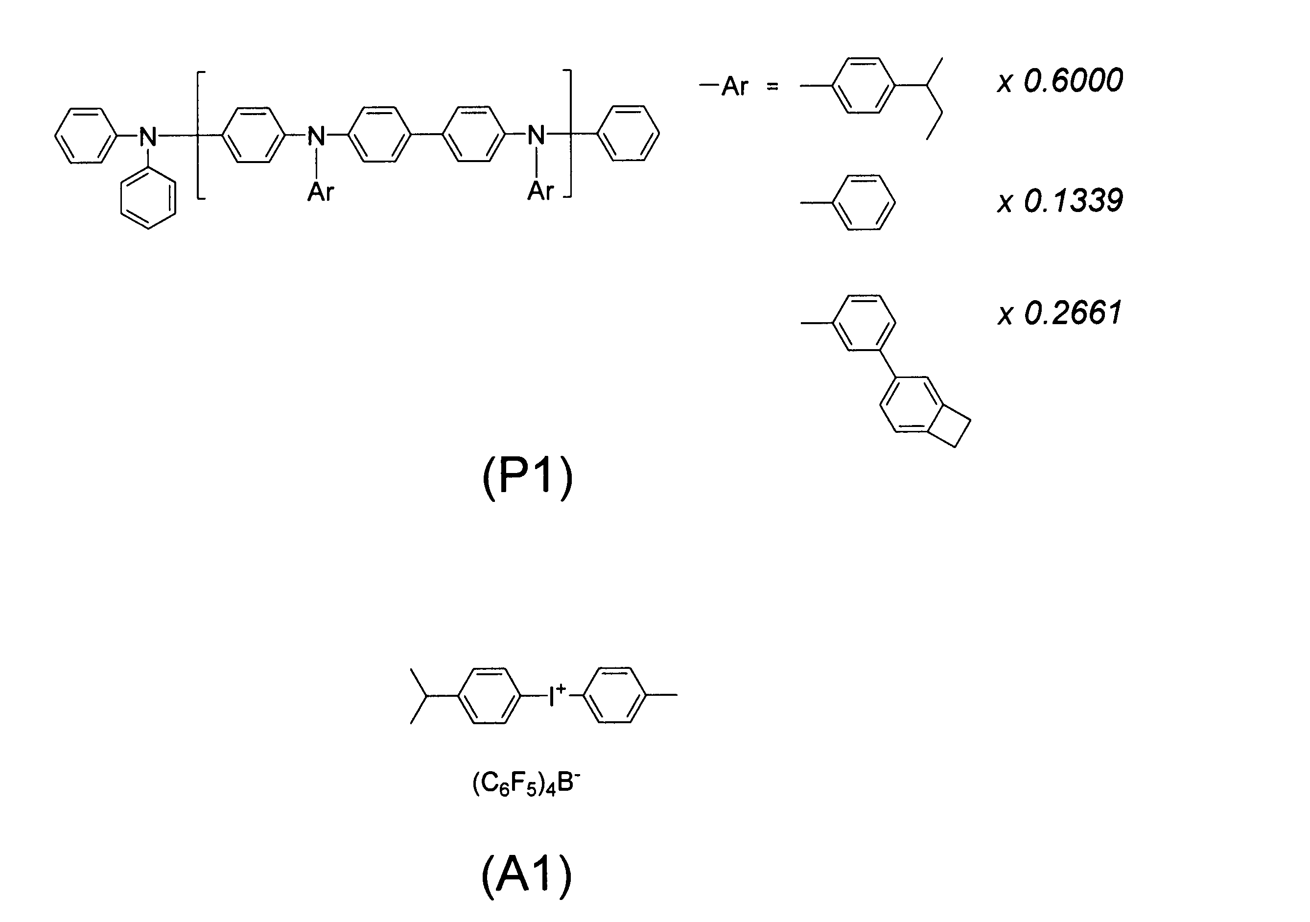
この正孔注入層形成用組成物を、下記に示す条件でスピンコート法により上記ITO基板上に塗布し、さらに下記に示すベーク条件にてベークすることにより、膜厚40nmの正孔注入層3を得た。
<成膜条件>
スピンコート雰囲気 大気雰囲気下
ベーク条件 大気雰囲気下、230℃、1時間
その後、下記(H1)で表される正孔輸送性高分子化合物の1質量%シクロヘキシルベンゼン溶液(正孔輸送層形成用組成物)を調製し、これを下記に示す条件で正孔注入層3上にスピンコートにて塗布し、ベークによる架橋処理を行うことで、膜厚10nmの正孔輸送層4を形成した。
スピンコート雰囲気 大気雰囲気下
ベーク条件 大気雰囲気下、230℃、1時間
その後、下記(H1)で表される正孔輸送性高分子化合物の1質量%シクロヘキシルベンゼン溶液(正孔輸送層形成用組成物)を調製し、これを下記に示す条件で正孔注入層3上にスピンコートにて塗布し、ベークによる架橋処理を行うことで、膜厚10nmの正孔輸送層4を形成した。
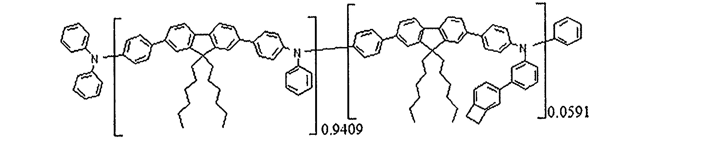
<成膜条件>
スピンコート雰囲気 窒素雰囲気下
ベーク条件 窒素雰囲気下、230℃、1時間
次に、発光層5を形成するにあたり、以下に示す発光材料(D-1)と、電荷輸送性化合物(h-1~h-3)、及びフェノール性化合物としてブチルヒドロキシアニソール(3-BHA)を用いて、下記に示す組成の発光層形成用組成物を調製した。
スピンコート雰囲気 窒素雰囲気下
ベーク条件 窒素雰囲気下、230℃、1時間
次に、発光層5を形成するにあたり、以下に示す発光材料(D-1)と、電荷輸送性化合物(h-1~h-3)、及びフェノール性化合物としてブチルヒドロキシアニソール(3-BHA)を用いて、下記に示す組成の発光層形成用組成物を調製した。
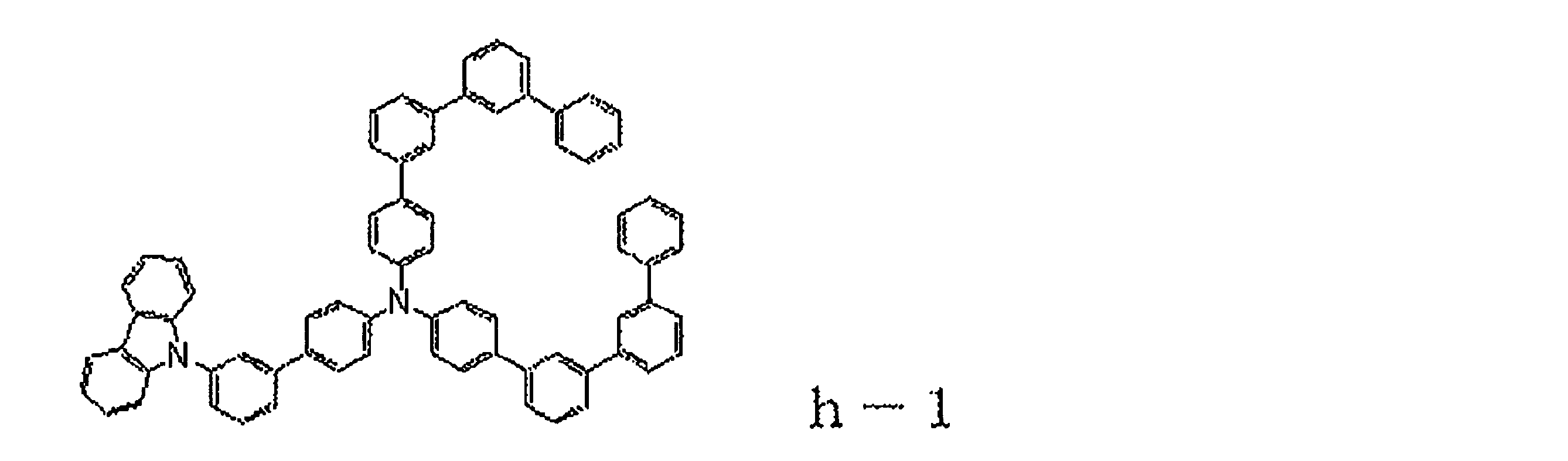
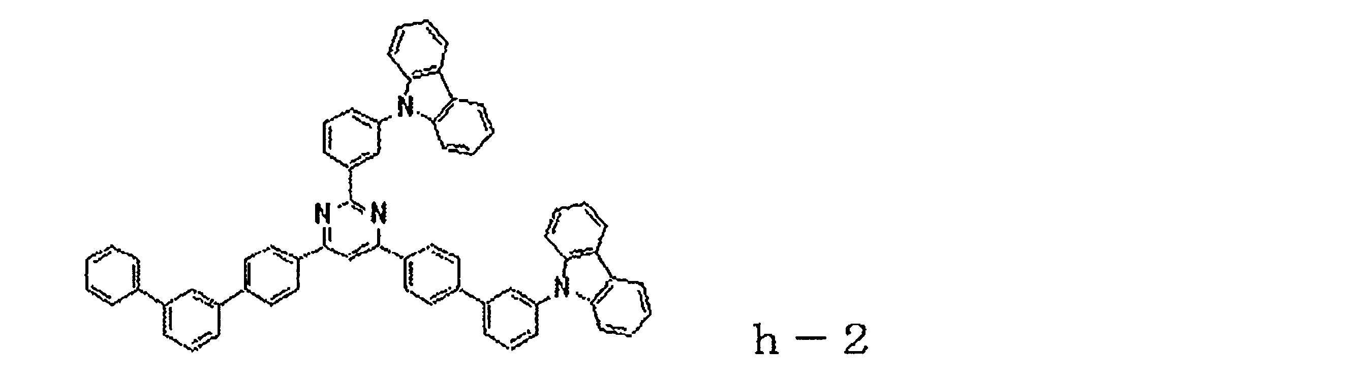
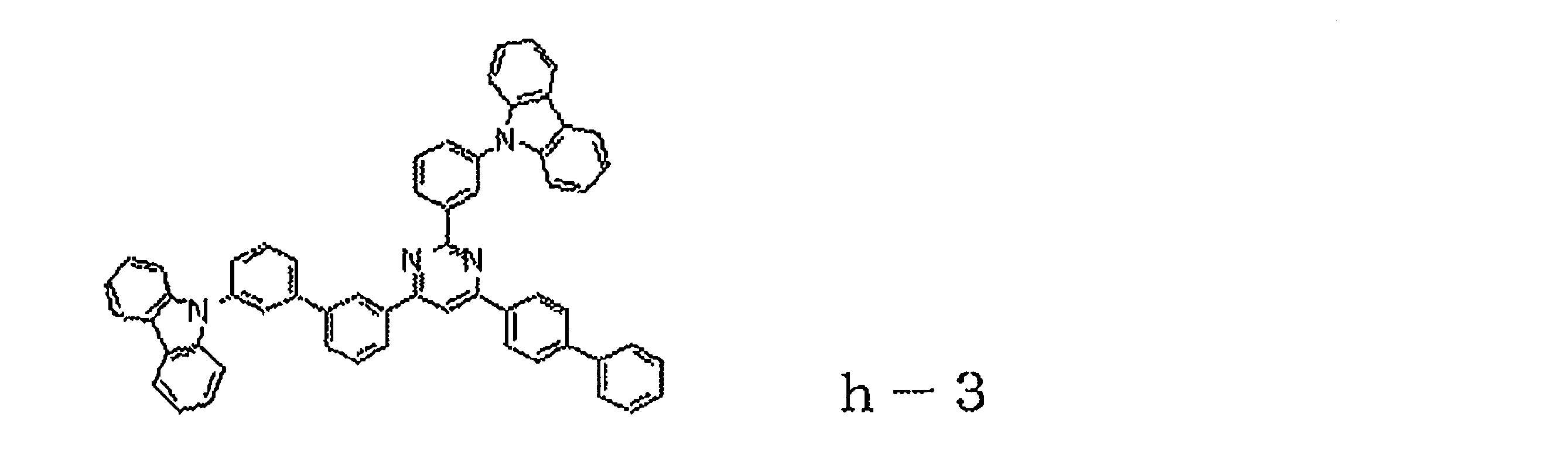
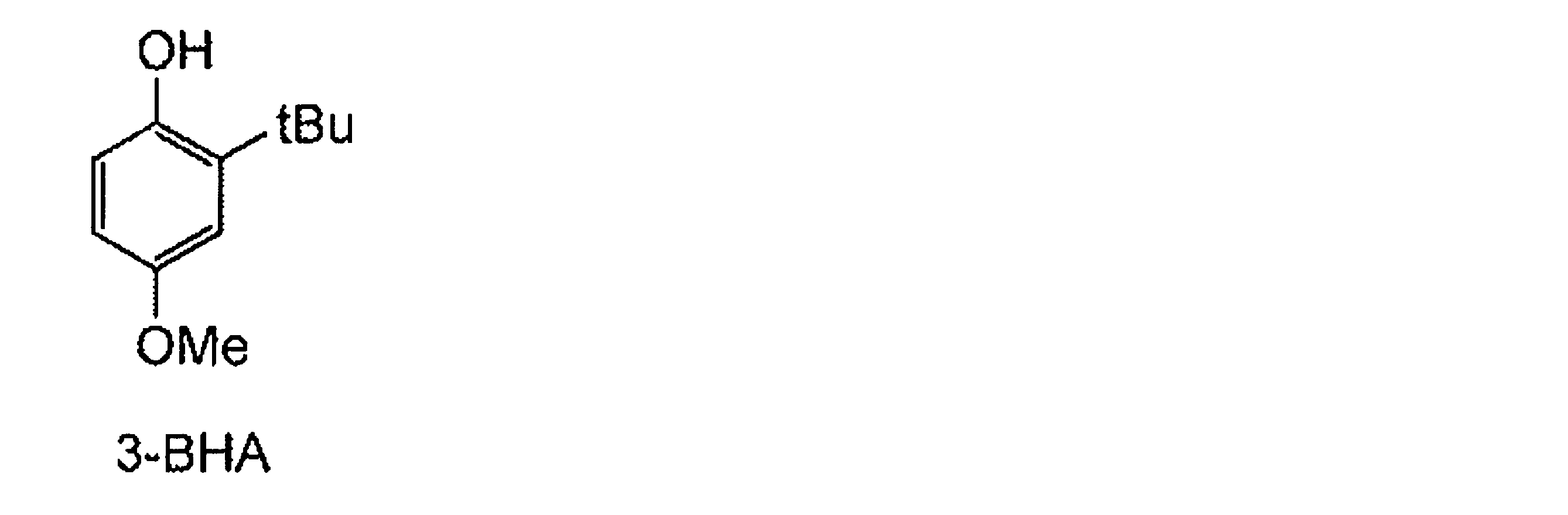
<発光層形成用組成物組成>
溶剤 シクロヘキシルベンゼン
成分濃度 (D-1):0.3質量%
(h-1):2.25質量%
(h-2):0.375質量%
(h-3):0.375質量%
3-BHA :0.01質量%
この発光層形成用組成物を調製した当日に、この溶液を用いて、以下に示す条件で正孔輸送層4上にスピンコート法にて塗布し、下記に示すベーク条件でベーク処理を行うことで、膜厚50nmの発光層5を形成した。
溶剤 シクロヘキシルベンゼン
成分濃度 (D-1):0.3質量%
(h-1):2.25質量%
(h-2):0.375質量%
(h-3):0.375質量%
3-BHA :0.01質量%
この発光層形成用組成物を調製した当日に、この溶液を用いて、以下に示す条件で正孔輸送層4上にスピンコート法にて塗布し、下記に示すベーク条件でベーク処理を行うことで、膜厚50nmの発光層5を形成した。
<成膜条件>
スピンコート雰囲気 窒素雰囲気下
ベーク条件 窒素雰囲気下、120℃、10分
次に、正孔注入層3、正孔輸送層4及び発光層5を湿式成膜した基板を真空蒸着装置内に搬入し、粗排気を行った後、クライオポンプを用いて装置内の真空度が3.0×10⁻⁴Pa以下になるまで排気した。発光層5の上に、真空度を2.2×10⁻⁴Pa以下に保った状態で、正孔阻止材料としてHB1を蒸着速度0.6~1.2Å/秒で膜厚10nm積層することにより正孔阻止層6を形成した。
スピンコート雰囲気 窒素雰囲気下
ベーク条件 窒素雰囲気下、120℃、10分
次に、正孔注入層3、正孔輸送層4及び発光層5を湿式成膜した基板を真空蒸着装置内に搬入し、粗排気を行った後、クライオポンプを用いて装置内の真空度が3.0×10⁻⁴Pa以下になるまで排気した。発光層5の上に、真空度を2.2×10⁻⁴Pa以下に保った状態で、正孔阻止材料としてHB1を蒸着速度0.6~1.2Å/秒で膜厚10nm積層することにより正孔阻止層6を形成した。
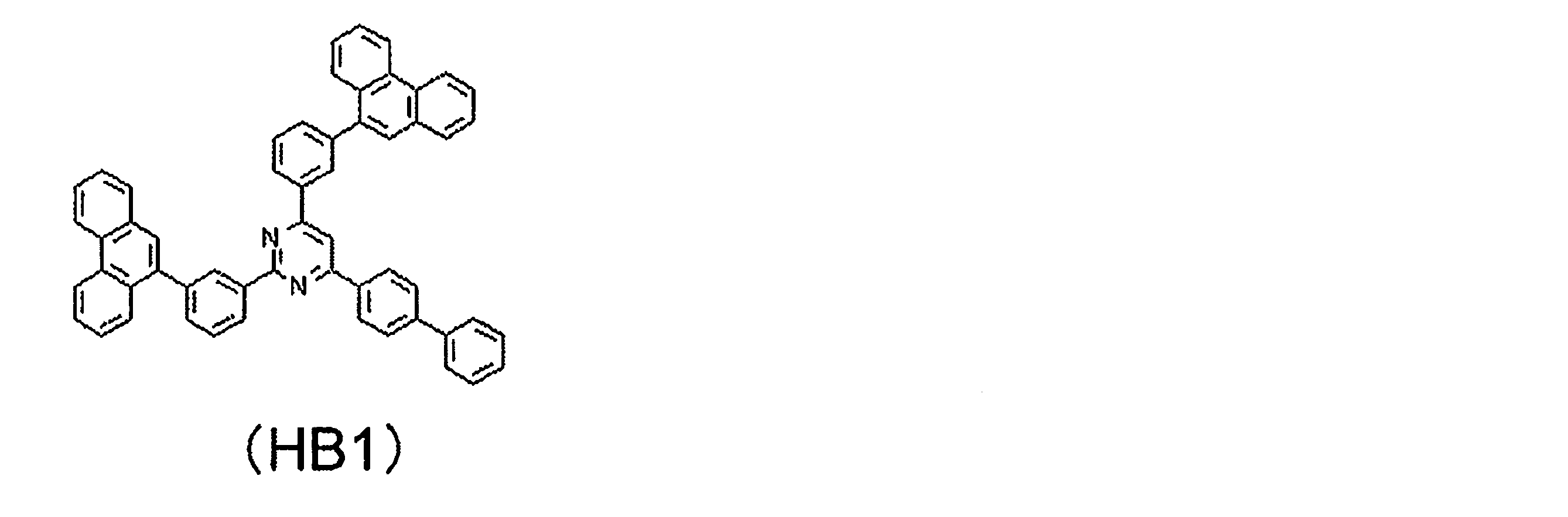
次いで、真空度を2.2×10⁻⁴Pa以下に保った状態で、正孔阻止層6の上に、トリス(8-ヒドロキシキノリナート)アルミニウム(Alq3)を加熱して、蒸着速度0.7~1.3Å/秒で膜厚20nm積層することにより電子輸送層7を形成した。
ここで、電子輸送層7までの蒸着を行った素子を、有機層蒸着用チャンバーから金属蒸着用チャンバーへと搬送した。陰極蒸着用のマスクとして2mm幅のストライプ状シャドーマスクを、陽極2のITOストライプと直交するように素子に密着させて設置した。有機層蒸着時と同様にして装置内を真空度が1.1×10⁻⁴Pa以下になるまで排気した。
ここで、電子輸送層7までの蒸着を行った素子を、有機層蒸着用チャンバーから金属蒸着用チャンバーへと搬送した。陰極蒸着用のマスクとして2mm幅のストライプ状シャドーマスクを、陽極2のITOストライプと直交するように素子に密着させて設置した。有機層蒸着時と同様にして装置内を真空度が1.1×10⁻⁴Pa以下になるまで排気した。
その後、真空度を1.0×10⁻⁴Pa以下に保った状態で、電子輸送層7の上に、フッ化リチウム(LiF)を、モリブデンボートを用いて加熱することにより蒸着速度0.07~0.15Å/秒で膜厚0.5nm積層することにより電子注入層8を形成した。次に、同様にして、真空度を2.0×10-4Paに保った状態で、アルミニウムを、モリブデンボートを用いて加熱することにより、蒸着速度0.6~10.0Å/秒で膜厚80nm蒸着することにより、陰極9を形成した。以上の電子注入層8及び陰極9の蒸着時の基板温度は、室温に保持した。
引き続き、素子が保管中に大気中の水分等で劣化することを防ぐため、以下に記載の方法で封止処理を行った。
窒素グローブボックス中で、23mm×23mmサイズのガラス板の外周部に、1mmの幅で光硬化性樹脂30Y-437(スリーボンド社製)を塗布し、中央部に水分ゲッターシート(ダイニック社製)を設置した。この上に、陰極の形成を終了した基板を搬入し、蒸着された面が乾燥剤シートと対向するように貼り合わせた。その後、光硬化性樹脂が塗布された領域のみに紫外光を照射し、樹脂を硬化させた。
窒素グローブボックス中で、23mm×23mmサイズのガラス板の外周部に、1mmの幅で光硬化性樹脂30Y-437(スリーボンド社製)を塗布し、中央部に水分ゲッターシート(ダイニック社製)を設置した。この上に、陰極の形成を終了した基板を搬入し、蒸着された面が乾燥剤シートと対向するように貼り合わせた。その後、光硬化性樹脂が塗布された領域のみに紫外光を照射し、樹脂を硬化させた。
以上の様にして、2mm×2mmのサイズの発光面積部分を有し、ピーク波長560nmで発光する有機電界発光素子が得られた。
[実施例2]
フェノール性化合物として3-BHAの代わりに、4,4’-ブチリデンビス(6-t-ブチル-3-メチルフェノール)を用いた以外は、実施例1と同様に操作することで、実施例2の有機電界発光素子を得た。
フェノール性化合物として3-BHAの代わりに、4,4’-ブチリデンビス(6-t-ブチル-3-メチルフェノール)を用いた以外は、実施例1と同様に操作することで、実施例2の有機電界発光素子を得た。

[実施例3]
フェノール性化合物として3-BHAの代わりに、2,6-ジ-tert-ブチルフェノール(BHB)を用いた以外は、実施例1と同様に操作することで、実施例2の有機電界発光素子を得た。
フェノール性化合物として3-BHAの代わりに、2,6-ジ-tert-ブチルフェノール(BHB)を用いた以外は、実施例1と同様に操作することで、実施例2の有機電界発光素子を得た。

[比較例1]
フェノール性化合物を用いないこと以外は、実施例1と同様の操作をすることで、比較例1の有機電界発光素子を得た。
フェノール性化合物を用いないこと以外は、実施例1と同様の操作をすることで、比較例1の有機電界発光素子を得た。
[比較例2]
フェノール性化合物として3-BHAの代わりに、2,6-ジ-tert-ブチル-4-メチル-フェノール(BHT)を用いた以外は、実施例1と同様に操作することで、実施例2の有機電界発光素子を得た。
フェノール性化合物として3-BHAの代わりに、2,6-ジ-tert-ブチル-4-メチル-フェノール(BHT)を用いた以外は、実施例1と同様に操作することで、実施例2の有機電界発光素子を得た。
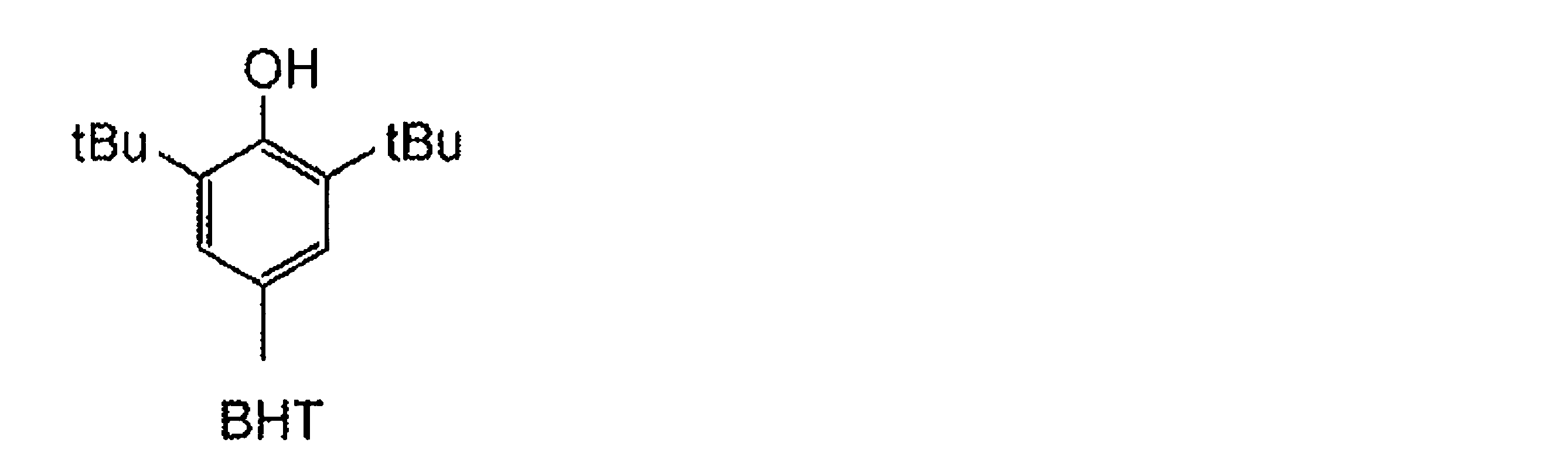
[比較例3]
フェノール性化合物として3-BHAの代わりに、Irganox1330を用いた以外は、実施例1と同様に操作することで、比較例3の有機電界発光素子を得た。
フェノール性化合物として3-BHAの代わりに、Irganox1330を用いた以外は、実施例1と同様に操作することで、比較例3の有機電界発光素子を得た。

[比較例4]
フェノール性化合物として3-BHAの代わりに、4-tert-オクチルフェノールを用いた以外は、実施例1と同様に操作することで、比較例4の有機電界発光素子を得た。
フェノール性化合物として3-BHAの代わりに、4-tert-オクチルフェノールを用いた以外は、実施例1と同様に操作することで、比較例4の有機電界発光素子を得た。
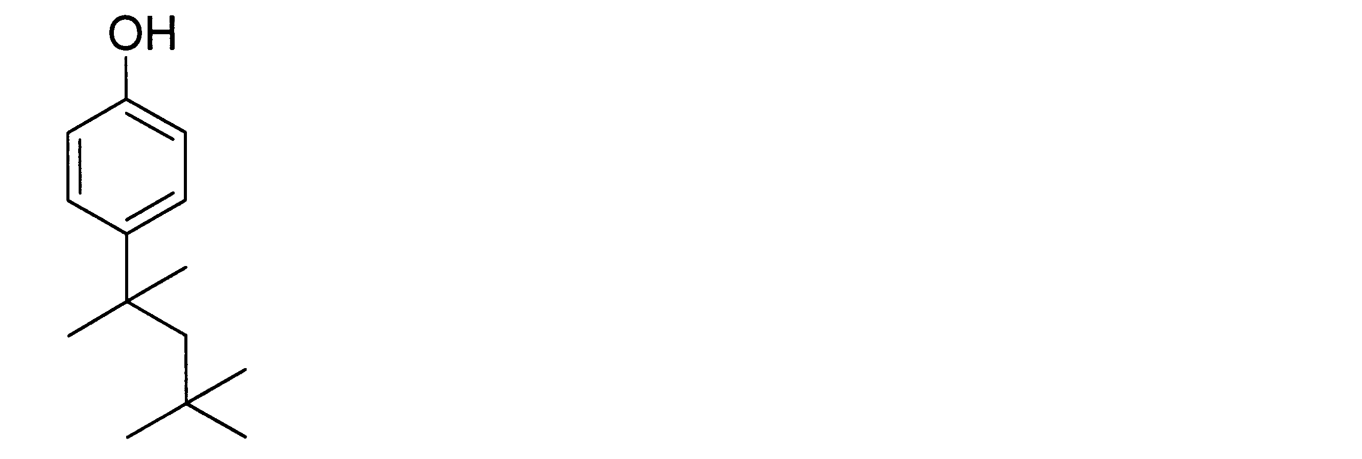
実施例1~3、比較例1~4について、それぞれ、10mA/cm2の電流を流した時の輝度電流効率と初期輝度5000cd/m2の時の電流値を用いた直流電流駆動における50時間後の相対輝度を測定した。比較例1を基準とした時のそれぞれの変化率(相対値)及び50時間後の相対輝度率の差を表1にまとめた。実施例1~3では劇的に輝度電流効率が上昇しており、オルト及びパラ位全てにアルキル基の置換がされている比較例2,3では若干効率が上昇しているにとどまっている。また、パラ位のみにアルキル置換したフェノール性を用いると、輝度電流効率の低下が起こっていることが確認できた。
輝度電流効率の変化率(相対値):
対象とする実施例または比較例の電流効率をηE(cd/A)、比較例1の電流効率をηR(cd/A)とした場合、
輝度電流効率の変化率(相対値)=(ηE/ηR-1)×100(%)
50時間後の相対輝度率の差:
50時間後の輝度をL50(cd/m2)とした場合、初期輝度は5000(cd/m2)なので、
50時間後の相対輝度率=L50/5000×100(%)。
対象とする実施例または比較例の50時間後の相対輝度率をτE(%)、
比較例1の50時間後の相対輝度率をτR(%)とした場合、
50時間後の相対輝度率の差=(τE-τR)(%)
輝度電流効率の変化率(相対値):
対象とする実施例または比較例の電流効率をηE(cd/A)、比較例1の電流効率をηR(cd/A)とした場合、
輝度電流効率の変化率(相対値)=(ηE/ηR-1)×100(%)
50時間後の相対輝度率の差:
50時間後の輝度をL50(cd/m2)とした場合、初期輝度は5000(cd/m2)なので、
50時間後の相対輝度率=L50/5000×100(%)。
対象とする実施例または比較例の50時間後の相対輝度率をτE(%)、
比較例1の50時間後の相対輝度率をτR(%)とした場合、
50時間後の相対輝度率の差=(τE-τR)(%)

本発明を特定の態様を用いて詳細に説明したが、本発明の意図と範囲を離れることなく様々な変更および変形が可能であることは、当業者にとって明らかである。なお本出願は、2015年3月24日付で出願された日本特許出願(特願2015-061261)および2015年10月16日付で出願された日本特許出願(特願2015-204901)に基づいており、その全体が引用により援用される。
1 基板
2 陽極
3 正孔注入層
4 正孔輸送層
5 発光層
6 正孔阻止層
7 電子輸送層
8 電子注入層
9 陰極
10 有機電界発光素子
2 陽極
3 正孔注入層
4 正孔輸送層
5 発光層
6 正孔阻止層
7 電子輸送層
8 電子注入層
9 陰極
10 有機電界発光素子
Claims (10)
- 少なくとも燐光発光材料、電荷輸送性化合物、及びフェノール性水酸基を有し且つ、該フェノール性水酸基を1位としたときに2,4,6位にはいずれか2つにのみ置換基を有するフェノール性化合物を含有する有機電界発光素子用組成物。
- 前記フェノール性化合物中にフェノール構造が1つのみである請求項1に記載の有機電界発光素子用組成物。
- 前記フェノール性化合物が、フェノール性水酸基を1位としたときに2,4,6位のいずれか2つのみ置換基を有し、3位及び5位は無置換であるフェノール性化合物である、請求項1又は2に記載の有機電界発光素子用組成物。
- 前記置換基が、炭素数1~12のアルキル基、炭素数1~12のアルコキシ基、炭素数6~18のアリール基を用いたアリールオキシ基、炭素数1~24のアラルキル基から選ばれる請求項1~3のいずれか1項に記載の有機電界発光素子用組成物。
- 前記置換基が、炭素数1~12のアルキル基または炭素数1~12のアルコキシ基から選ばれる請求項1~4のいずれか1項に記載の有機電界発光素子用組成物。
- 前記フェノール性化合物が、前記組成物中の前記電荷輸送性化合物の総量に対して、0.01質量%以上、10質量%以下である請求項1~5のいずれか1項に記載の有機電界発光素子用組成物。
- 前記フェノール性化合物が、前記組成物中に含まれる前記電荷輸送性化合物の総量に対して、0.1質量%以上、1質量%以下である請求項1~6のいずれか1項に記載の有機電界発光素子用組成物。
- 陽極、陰極、及び前記陽極と前記陰極の間に少なくとも1層の発光層を有する有機電界発光素子であって、前記発光層の少なくとも1層が、請求項1~7のいずれか1項に記載の有機電界発光素子用組成物を用いて湿式成膜することによって形成された有機電界発光素子。
- 請求項8に記載の有機電界発光素子を有する表示装置。
- 請求項8に記載の有機電界発光素子を有する照明装置。
Priority Applications (4)
| Application Number | Priority Date | Filing Date | Title |
|---|---|---|---|
| KR1020177008439A KR102270975B1 (ko) | 2015-03-24 | 2016-03-22 | 유기 전계 발광 소자용 조성물, 유기 전계 발광 소자, 표시 장치 및 조명 장치 |
| KR1020217012785A KR102379434B1 (ko) | 2015-03-24 | 2016-03-22 | 유기 전계 발광 소자용 조성물, 유기 전계 발광 소자, 표시 장치 및 조명 장치 |
| CN201680002976.XA CN106716669B (zh) | 2015-03-24 | 2016-03-22 | 有机电致发光元件用组合物、有机电致发光元件、显示装置以及照明装置 |
| KR1020197035327A KR102329599B1 (ko) | 2015-03-24 | 2016-03-22 | 유기 전계 발광 소자용 조성물, 유기 전계 발광 소자, 표시 장치 및 조명 장치 |
Applications Claiming Priority (4)
| Application Number | Priority Date | Filing Date | Title |
|---|---|---|---|
| JP2015061261 | 2015-03-24 | ||
| JP2015-061261 | 2015-03-24 | ||
| JP2015204901A JP5874860B1 (ja) | 2015-03-24 | 2015-10-16 | 有機電界発光素子用組成物及び有機電界発光素子の製造方法 |
| JP2015-204901 | 2015-10-16 |
Publications (1)
| Publication Number | Publication Date |
|---|---|
| WO2016152880A1 true WO2016152880A1 (ja) | 2016-09-29 |
Family
ID=55434661
Family Applications (1)
| Application Number | Title | Priority Date | Filing Date |
|---|---|---|---|
| PCT/JP2016/059057 Ceased WO2016152880A1 (ja) | 2015-03-24 | 2016-03-22 | 有機電界発光素子用組成物、有機電界発光素子、表示装置及び照明装置 |
Country Status (5)
| Country | Link |
|---|---|
| JP (1) | JP5874860B1 (ja) |
| KR (3) | KR102379434B1 (ja) |
| CN (1) | CN106716669B (ja) |
| TW (1) | TWI609874B (ja) |
| WO (1) | WO2016152880A1 (ja) |
Families Citing this family (3)
| Publication number | Priority date | Publication date | Assignee | Title |
|---|---|---|---|---|
| WO2019146396A1 (ja) * | 2018-01-24 | 2019-08-01 | コニカミノルタ株式会社 | 発光性薄膜、発光性積層膜、有機エレクトロルミネッセンス素子、及びその製造方法 |
| FR3098821B1 (fr) * | 2019-07-19 | 2023-05-26 | Isorg | Encre pour une couche d’injection d’électrons |
| CN114127977A (zh) * | 2019-07-19 | 2022-03-01 | 爱色乐居 | 沉积电子注入层的方法 |
Citations (6)
| Publication number | Priority date | Publication date | Assignee | Title |
|---|---|---|---|---|
| JPH09125054A (ja) * | 1995-09-21 | 1997-05-13 | Bayer Ag | 電界発光装置 |
| JPH10255981A (ja) * | 1997-03-13 | 1998-09-25 | Sumitomo Chem Co Ltd | 有機エレクトロルミネッセンス素子 |
| JP2001351785A (ja) * | 2000-06-09 | 2001-12-21 | Sumitomo Chem Co Ltd | 有機エレクトロルミネッセンス素子 |
| JP2013060396A (ja) * | 2011-09-13 | 2013-04-04 | Konica Minolta Holdings Inc | 縮合複素環化合物の製造方法 |
| JP2013165089A (ja) * | 2010-09-30 | 2013-08-22 | Fujifilm Corp | 有機電界発光素子用組成物、並びに、該組成物を用いた膜、発光層、電荷輸送層、有機電界発光素子、発光層の形成方法及び電荷輸送層の形成方法 |
| JP2015093938A (ja) * | 2013-11-12 | 2015-05-18 | 三菱化学株式会社 | 有機電界発光素子用組成物、有機電界発光素子、表示装置及び照明装置 |
Family Cites Families (7)
| Publication number | Priority date | Publication date | Assignee | Title |
|---|---|---|---|---|
| JP2004088094A (ja) | 2002-07-01 | 2004-03-18 | Seiko Epson Corp | 組成物、成膜方法及び成膜装置、電気光学装置及びその製造方法、有機エレクトロルミネッセンス装置及びその製造方法、デバイス及びその製造方法、電子機器 |
| US8034465B2 (en) * | 2007-06-20 | 2011-10-11 | Global Oled Technology Llc | Phosphorescent oled having double exciton-blocking layers |
| KR20120093354A (ko) * | 2009-12-15 | 2012-08-22 | 미쓰비시 가가꾸 가부시키가이샤 | 유기 전계 발광 소자의 제조 방법, 유기 전계 발광 소자, 표시 장치 및 조명 장치 |
| JP2012033918A (ja) * | 2010-07-08 | 2012-02-16 | Mitsubishi Chemicals Corp | 有機電界発光素子、有機電界発光デバイス、有機el表示装置及び有機el照明 |
| WO2012070226A1 (ja) | 2010-11-22 | 2012-05-31 | 出光興産株式会社 | 含酸素縮合環誘導体及びそれを含んでなる有機エレクトロルミネッセンス素子 |
| JP5182441B1 (ja) * | 2012-05-24 | 2013-04-17 | 三菱化学株式会社 | 有機電界発光素子、有機電界発光照明装置及び有機電界発光表示装置 |
| JP5823585B2 (ja) * | 2013-08-28 | 2015-11-25 | 住友化学株式会社 | 燐光発光材料を含有する液状組成物 |
-
2015
- 2015-10-16 JP JP2015204901A patent/JP5874860B1/ja active Active
-
2016
- 2016-03-22 WO PCT/JP2016/059057 patent/WO2016152880A1/ja not_active Ceased
- 2016-03-22 KR KR1020217012785A patent/KR102379434B1/ko active Active
- 2016-03-22 KR KR1020177008439A patent/KR102270975B1/ko active Active
- 2016-03-22 CN CN201680002976.XA patent/CN106716669B/zh active Active
- 2016-03-22 KR KR1020197035327A patent/KR102329599B1/ko active Active
- 2016-03-24 TW TW105109148A patent/TWI609874B/zh active
Patent Citations (6)
| Publication number | Priority date | Publication date | Assignee | Title |
|---|---|---|---|---|
| JPH09125054A (ja) * | 1995-09-21 | 1997-05-13 | Bayer Ag | 電界発光装置 |
| JPH10255981A (ja) * | 1997-03-13 | 1998-09-25 | Sumitomo Chem Co Ltd | 有機エレクトロルミネッセンス素子 |
| JP2001351785A (ja) * | 2000-06-09 | 2001-12-21 | Sumitomo Chem Co Ltd | 有機エレクトロルミネッセンス素子 |
| JP2013165089A (ja) * | 2010-09-30 | 2013-08-22 | Fujifilm Corp | 有機電界発光素子用組成物、並びに、該組成物を用いた膜、発光層、電荷輸送層、有機電界発光素子、発光層の形成方法及び電荷輸送層の形成方法 |
| JP2013060396A (ja) * | 2011-09-13 | 2013-04-04 | Konica Minolta Holdings Inc | 縮合複素環化合物の製造方法 |
| JP2015093938A (ja) * | 2013-11-12 | 2015-05-18 | 三菱化学株式会社 | 有機電界発光素子用組成物、有機電界発光素子、表示装置及び照明装置 |
Also Published As
| Publication number | Publication date |
|---|---|
| KR102329599B1 (ko) | 2021-11-22 |
| KR20170048473A (ko) | 2017-05-08 |
| KR102270975B1 (ko) | 2021-07-01 |
| CN106716669A (zh) | 2017-05-24 |
| KR102379434B1 (ko) | 2022-03-28 |
| KR20210049980A (ko) | 2021-05-06 |
| JP2016181669A (ja) | 2016-10-13 |
| KR20190135567A (ko) | 2019-12-06 |
| JP5874860B1 (ja) | 2016-03-02 |
| TWI609874B (zh) | 2018-01-01 |
| CN106716669B (zh) | 2019-12-31 |
| TW201700490A (zh) | 2017-01-01 |
Similar Documents
| Publication | Publication Date | Title |
|---|---|---|
| JP5757244B2 (ja) | 有機電界発光素子の製造方法、有機電界発光素子、表示装置及び照明装置 | |
| JP5577685B2 (ja) | 有機電界発光素子の製造方法、有機電界発光素子、有機el表示装置及び有機el照明 | |
| JP5884213B2 (ja) | 有機電界発光素子の製造方法、有機電界発光素子、有機elディスプレイ及び有機el照明 | |
| JP6035706B2 (ja) | 有機電界素子用組成物の製造方法、有機電界素子用組成物、有機電界発光素子の製造方法、有機電界発光素子、有機el表示装置および有機el照明 | |
| JP2015093938A (ja) | 有機電界発光素子用組成物、有機電界発光素子、表示装置及び照明装置 | |
| JP2010202644A (ja) | 有機金属錯体、有機金属錯体含有組成物、発光材料、有機電界発光素子材料、有機電界発光素子、有機elディスプレイおよび有機el照明 | |
| JP6217059B2 (ja) | 有機電界発光素子及び有機電界発光デバイス | |
| JP6264766B2 (ja) | イリジウム錯体化合物、有機電界発光素子、表示装置ならびに照明装置 | |
| WO2018135656A1 (ja) | 発光層形成用組成物及び該発光層形成用組成物を含有する有機電界発光素子 | |
| JP2009252407A (ja) | 有機電界発光素子の製造方法 | |
| JP2012077043A (ja) | 有機金属錯体、有機金属錯体含有組成物、発光材料、有機電界発光素子材料、有機電界発光素子、有機電界発光素子表示装置および有機界発光素子照明装置 | |
| JP5874860B1 (ja) | 有機電界発光素子用組成物及び有機電界発光素子の製造方法 | |
| JP2014234360A (ja) | イリジウム錯体化合物、有機電界発光素子、表示装置および照明装置 | |
| JP5332690B2 (ja) | 有機金属錯体組成物、有機金属錯体含有組成物、有機電界発光素子、有機elディスプレイおよび有機el照明 | |
| JP2010199296A (ja) | 有機電界発光素子、有機elディスプレイおよび有機el照明 | |
| JP6724294B2 (ja) | 有機電界発光素子用組成物、有機電界発光素子、表示装置及び照明装置 | |
| JP6984674B2 (ja) | 有機電界発光素子用組成物、有機電界発光素子、表示装置及び照明装置 | |
| JP2010209248A (ja) | 有機電界発光素子用組成物、有機電界発光素子、有機elディスプレイおよび有機el照明 | |
| JP2018166102A (ja) | 有機電界発光素子用組成物、有機電界発光素子、表示装置及び照明装置 | |
| JP5708721B2 (ja) | 有機電界発光素子、有機el表示装置および有機el照明 | |
| JP2010212437A (ja) | 有機電界発光素子用組成物、有機電界発光素子、有機el表示装置および有機el照明 | |
| JP2021075493A (ja) | Oled素子形成用組成物及びoled素子 | |
| JP2010206003A (ja) | 有機電界発光素子用組成物、有機電界発光素子、有機elディスプレイおよび有機el照明 | |
| JP2014012672A (ja) | 有機金属錯体組成物、有機金属錯体含有組成物、有機電界発光素子、有機elディスプレイおよび有機el照明 |
Legal Events
| Date | Code | Title | Description |
|---|---|---|---|
| 121 | Ep: the epo has been informed by wipo that ep was designated in this application |
Ref document number: 16768783 Country of ref document: EP Kind code of ref document: A1 |
|
| ENP | Entry into the national phase |
Ref document number: 20177008439 Country of ref document: KR Kind code of ref document: A |
|
| NENP | Non-entry into the national phase |
Ref country code: DE |
|
| 122 | Ep: pct application non-entry in european phase |
Ref document number: 16768783 Country of ref document: EP Kind code of ref document: A1 |