WO2016152603A1 - 移相器、インピーダンス整合回路、合分波器および通信端末装置 - Google Patents
移相器、インピーダンス整合回路、合分波器および通信端末装置 Download PDFInfo
- Publication number
- WO2016152603A1 WO2016152603A1 PCT/JP2016/057914 JP2016057914W WO2016152603A1 WO 2016152603 A1 WO2016152603 A1 WO 2016152603A1 JP 2016057914 W JP2016057914 W JP 2016057914W WO 2016152603 A1 WO2016152603 A1 WO 2016152603A1
- Authority
- WO
- WIPO (PCT)
- Prior art keywords
- coil
- phase shifter
- port
- band
- impedance
- Prior art date
- Legal status (The legal status is an assumption and is not a legal conclusion. Google has not performed a legal analysis and makes no representation as to the accuracy of the status listed.)
- Ceased
Links
Images












Classifications
-
- H—ELECTRICITY
- H03—ELECTRONIC CIRCUITRY
- H03H—IMPEDANCE NETWORKS, e.g. RESONANT CIRCUITS; RESONATORS
- H03H7/00—Multiple-port networks comprising only passive electrical elements as network components
- H03H7/38—Impedance-matching networks
-
- H—ELECTRICITY
- H03—ELECTRONIC CIRCUITRY
- H03H—IMPEDANCE NETWORKS, e.g. RESONANT CIRCUITS; RESONATORS
- H03H7/00—Multiple-port networks comprising only passive electrical elements as network components
- H03H7/18—Networks for phase shifting
-
- H—ELECTRICITY
- H01—ELECTRIC ELEMENTS
- H01P—WAVEGUIDES; RESONATORS, LINES, OR OTHER DEVICES OF THE WAVEGUIDE TYPE
- H01P1/00—Auxiliary devices
- H01P1/18—Phase-shifters
- H01P1/184—Strip line phase-shifters
-
- H—ELECTRICITY
- H01—ELECTRIC ELEMENTS
- H01Q—ANTENNAS, i.e. RADIO AERIALS
- H01Q1/00—Details of, or arrangements associated with, antennas
- H01Q1/48—Earthing means; Earth screens; Counterpoises
-
- H—ELECTRICITY
- H01—ELECTRIC ELEMENTS
- H01Q—ANTENNAS, i.e. RADIO AERIALS
- H01Q21/00—Antenna arrays or systems
- H01Q21/06—Arrays of individually energised antenna units similarly polarised and spaced apart
- H01Q21/22—Antenna units of the array energised non-uniformly in amplitude or phase, e.g. tapered array or binomial array
-
- H—ELECTRICITY
- H01—ELECTRIC ELEMENTS
- H01Q—ANTENNAS, i.e. RADIO AERIALS
- H01Q5/00—Arrangements for simultaneous operation of antennas on two or more different wavebands, e.g. dual-band or multi-band arrangements
- H01Q5/30—Arrangements for providing operation on different wavebands
- H01Q5/307—Individual or coupled radiating elements, each element being fed in an unspecified way
- H01Q5/314—Individual or coupled radiating elements, each element being fed in an unspecified way using frequency dependent circuits or components, e.g. trap circuits or capacitors
- H01Q5/335—Individual or coupled radiating elements, each element being fed in an unspecified way using frequency dependent circuits or components, e.g. trap circuits or capacitors at the feed, e.g. for impedance matching
-
- H—ELECTRICITY
- H01—ELECTRIC ELEMENTS
- H01Q—ANTENNAS, i.e. RADIO AERIALS
- H01Q7/00—Loop antennas with a substantially uniform current distribution around the loop and having a directional radiation pattern in a plane perpendicular to the plane of the loop
-
- H—ELECTRICITY
- H03—ELECTRONIC CIRCUITRY
- H03H—IMPEDANCE NETWORKS, e.g. RESONANT CIRCUITS; RESONATORS
- H03H7/00—Multiple-port networks comprising only passive electrical elements as network components
- H03H7/01—Frequency selective two-port networks
- H03H7/0153—Electrical filters; Controlling thereof
- H03H7/0161—Bandpass filters
-
- H—ELECTRICITY
- H03—ELECTRONIC CIRCUITRY
- H03H—IMPEDANCE NETWORKS, e.g. RESONANT CIRCUITS; RESONATORS
- H03H7/00—Multiple-port networks comprising only passive electrical elements as network components
- H03H7/01—Frequency selective two-port networks
- H03H7/09—Filters comprising mutual inductance
-
- H—ELECTRICITY
- H03—ELECTRONIC CIRCUITRY
- H03H—IMPEDANCE NETWORKS, e.g. RESONANT CIRCUITS; RESONATORS
- H03H7/00—Multiple-port networks comprising only passive electrical elements as network components
- H03H7/18—Networks for phase shifting
- H03H7/20—Two-port phase shifters providing an adjustable phase shift
-
- H—ELECTRICITY
- H03—ELECTRONIC CIRCUITRY
- H03H—IMPEDANCE NETWORKS, e.g. RESONANT CIRCUITS; RESONATORS
- H03H9/00—Networks comprising electromechanical or electro-acoustic elements; Electromechanical resonators
- H03H9/46—Filters
- H03H9/64—Filters using surface acoustic waves
-
- H—ELECTRICITY
- H03—ELECTRONIC CIRCUITRY
- H03H—IMPEDANCE NETWORKS, e.g. RESONANT CIRCUITS; RESONATORS
- H03H9/00—Networks comprising electromechanical or electro-acoustic elements; Electromechanical resonators
- H03H9/70—Multiple-port networks for connecting several sources or loads, working on different frequencies or frequency bands, to a common load or source
- H03H9/72—Networks using surface acoustic waves
- H03H9/725—Duplexers
Definitions
- the present invention relates to a phase shifter provided in a high-frequency circuit, and more particularly to a phase shifter that performs phase shift according to a frequency band.
- the present invention also relates to an impedance matching circuit, and more particularly to an impedance matching circuit including a phase shifter.
- the present invention also relates to a multiplexer / demultiplexer, and more particularly, to a multiplexer / demultiplexer including a phase shifter.
- the present invention also relates to a communication terminal device including the phase shifter, the impedance matching circuit, or the multiplexer / demultiplexer.
- a phase shifter may be used for impedance matching in a high-frequency circuit.
- a high-pass filter type and a low-pass filter type phase shifter there are a high-pass filter type and a low-pass filter type phase shifter, and circuit constants are determined so as to obtain a desired phase shift amount at a desired frequency.
- Patent Document 1 discloses a phase shifter including a high-pass filter type circuit and a low-pass filter type circuit.
- phase shifter 73 is provided between the impedance matching circuit 72 and the second high frequency circuit 74, and the first high frequency circuit 71 and the first high frequency circuit 71 are connected to each other by the phase shifter 73 and the impedance matching circuit 72.
- the phase shifter is required to have a phase shift characteristic corresponding to the frequency band.
- phase shifting operations when impedance matching is performed for both the low band and the high band, it may be necessary to largely shift the phase of the other band without shifting the phase of one band. For example, there are the following two phase shifting operations.
- the passing phase of the low band signal is around 0 ° (or 180 °), and the passing phase of the high band signal is around 90 °.
- the passing phase of the low band signal is around 90 °
- the passing phase of the high band signal is around 0 ° or 180 °.
- the reflected wave from the second high-frequency circuit 74 reciprocates through the phase shifter 73, so that the amount of phase shift of the reflected signal at the phase shifter 73 is doubled. That is, a phase shift amount of 90 ° is necessary to set the reflection phase to 180 °, and a phase shift amount of 0 ° or 180 ° is required to set the reflection phase to 0 °.
- phase shifter that can perform a phase shift operation for each frequency band as shown in the above (1) and (2) as shown below.
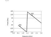
- FIG. 31 shows an example of the phase frequency characteristics of the high-pass filter type phase shifter shown in FIG.
- the phase shift amount in the low band (700 MHz band) can be 90 °, but the phase shift amount in the high band (2 GHz band) is not 0 ° but 30 °.
- FIG. 32 shows an example of the phase frequency characteristics of the low-pass filter type phase shifter shown in FIG.
- the phase shift amount in the low band (700 MHz band) can be ⁇ 90 °, but the phase shift amount in the high band (2 GHz band) is not about 180 ° but about 100 °. In both the low band and the high band, the change in the amount of phase shift in the frequency band is large.
- FIG. 33 is a characteristic example of the phase versus insertion loss of the high-pass filter type phase shifter shown in FIG. Since the phase shift amount is 180 ° in the vicinity of the cutoff frequency, the insertion loss increases when the phase shift amount is increased. In addition, in the low-pass filter type phase shifter shown in FIG. 30B, when a phase shift amount near 180 ° is obtained in the low band, the cut-off frequency becomes low, and the insertion loss in the high band is very large. Become.
- the conventional filter-type phase shifter cannot perform the phase shift operation for each frequency band as shown in the above (1) and (2).
- each filter cannot obtain its own characteristics.
- FIG. 36 is a circuit diagram of a diplexer composed of a high pass filter HPF and a low pass filter LPF.
- an antenna ANT is connected to a common port of the high pass filter HPF and the low pass filter LPF.
- a high band circuit is connected to the individual port of the high pass filter HPF, and a low band circuit is connected to the individual port of the low pass filter LPF.
- the high-pass filter HPF includes shunt-connected inductors L11 and L12 and a series-connected capacitor C11.
- the low-pass filter LPF includes series-connected inductors L21 and L22 and a shunt-connected capacitor C21.
- the inductor L11 of the high-pass filter HPF when the impedance of the inductor L11 of the high-pass filter HPF becomes very small in the low-band frequency band, the inductor L11 substantially becomes a short element, and a short element ( L11) is connected, and the isolation between the low-band circuit and the high-band circuit deteriorates in the low-band frequency band.
- a filter that is substantially short-circuited in another frequency band is connected to a common port in a certain frequency band is not limited to a diplexer that is a combination of a high-pass filter and a low-pass filter. The same occurs for a multiplexer or the like by a combination of a plurality of bandpass filters.
- An object of the present invention includes a phase shifter suitable for impedance matching, an impedance matching circuit including the phase shifter, a multiplexer / demultiplexer in which interference between a plurality of filters is suppressed, and the phase shifter and multiplexer / demultiplexer. It is to provide a communication terminal device.
- the phase shifter of the present invention is A transformer connected between the first port and the second port, having a second coil magnetically coupled to the first coil and the first coil, and including a parasitic inductance component;
- An impedance adjustment circuit having a reactance element that suppresses a shift in impedance due to a parasitic inductance component of the transformer; With The coupling coefficient between the first coil and the second coil of the transformer and the value of the reactance element of the impedance adjustment circuit are determined so that the amount of phase shift varies depending on the frequency band.
- the phase shifter of the present invention is A transformer connected between the first port and the second port, having a second coil magnetically coupled to the first coil and the first coil, and including a parasitic inductance component; An impedance adjustment circuit having a reactance element that suppresses a shift in impedance due to a parasitic inductance component of the transformer; With The phase shift amount in the low band is larger than the phase shift amount in the high band, and the phase shift amount in the low band is closer to 180 ° than 90 °, and the phase shift amount in the high band is 90 ° from 180 °. The coupling coefficient between the first coil and the second coil of the transformer and the value of the reactance element of the impedance adjustment circuit are determined so that the phase shift amount is close to.
- impedance matching according to the frequency band can be easily performed by reducing the difference in impedance between the low band and the high band.
- the phase shifter of the present invention is A transformer connected between the first port and the second port, having a second coil magnetically coupled to the first coil and the first coil, and including a parasitic inductance component;
- An impedance adjustment circuit having a reactance element that suppresses a shift in impedance due to a parasitic inductance component of the transformer;
- the amount of phase shift in the low band is larger than the amount of phase shift in the high band, the amount of phase shift in the low band is closer to 90 ° than 0 °, and the amount of phase shift in the high band is 0 ° from 90 °.
- the coupling coefficient between the first coil and the second coil of the transformer and the value of the reactance element of the impedance adjustment circuit are determined so that the phase shift amount is close to.
- impedance matching according to the frequency band can be easily performed by combining with an impedance matching circuit using a transformer.
- the impedance adjustment circuit is A first capacitance element connected between the first port of the transformer and ground; A second capacitance element connected between the second port of the transformer and the ground; A third capacitance element connected between the first port and the second port of the transformer; It is preferable to contain.
- the transformer impedance deviates from a specified value (for example, 50 ⁇ ) due to the presence of the parallel parasitic inductance component and the series parasitic inductance component of the transformer, but by providing the reactance element (capacitance element), the impedance Can be adjusted.
- a specified value for example, 50 ⁇
- the impedance adjustment circuit is A first capacitance element connected between the first port of the transformer and ground; A second capacitance element connected between the second port of the transformer and the ground; A series circuit of a third capacitance element and an inductance element connected between the first port and the second port of the transformer; It is preferable to contain.
- the series circuit of the third capacitance element and the inductance element can give the phase shift amount a predetermined frequency characteristic, and a predetermined phase shift amount corresponding to the frequency can be obtained over a wide frequency band.
- the presence of the parallel parasitic inductance component and the series parasitic inductance component included in the transformer causes the impedance of the transformer to deviate from a specified value (for example, 50 ⁇ ).
- a specified value for example, 50 ⁇ .
- the third capacitance element is mainly composed of an inter-coil capacitance generated between the first coil and the second coil. This eliminates the need for the pattern for forming the third capacitance element, or eliminates the need for the third capacitance element as a component, thereby reducing the size and cost.
- the first capacitance element is mainly composed of a line capacitance of the first coil
- the second capacitance element is mainly composed of the second coil. It is preferable that it is comprised by the capacity
- the transformer ratio between the first coil and the second coil is 1: n (n is a value other than 1),
- n is a value other than 1
- the reflection amount (impedance) of the phase shift amount by the phase shifter is moved from the high impedance side on the Smith chart to the low impedance side, and is moved toward the center on the Smith chart by the impedance conversion of the phase shifter. It is preferable.
- the impedance can be converted by the transformer together with the phase shift, and the function of the impedance matching circuit between the circuit connected to the first port and the circuit connected to the second port can be achieved.
- the transformer is provided in a single laminated body in which a plurality of base material layers are laminated, and the first coil and the second coil are the bases. It is preferable to be composed of a conductor pattern formed in the material layer. As a result, it is only necessary to mount the phase shifter as a single component on a printed wiring board or the like, and mounting on a communication terminal device or the like is facilitated.
- the first coil and the second coil have substantially the same inner and outer diameters, and the coil winding axis is coaxial.
- a transformer having an appropriate coupling coefficient can be obtained while the number of turns of the first coil and the second coil is small, that is, the size is small.
- phase shifter In any one of the above (1) to (10), it is preferable to further include a high-pass filter or a low-pass filter connected in series to the phase shifter. This makes it possible to determine the amount of phase shift that cannot be obtained only by the phase shifter.
- the high-pass filter or the low-pass filter preferably includes a capacitance element and an inductance element, and the inductance element is preferably magnetically coupled to the first coil or the second coil. According to this configuration, the frequency characteristic of the phase shift amount can be controlled.
- An impedance matching circuit of the present invention includes the phase shifter according to any one of (1) to (12) above, and an impedance matching circuit unit connected in series to the phase shifter,
- the impedance matching circuit unit is a circuit that performs impedance matching with respect to the impedance phase-shifted by the phase shifter.
- the impedance matching circuit unit is preferably a circuit unit that moves both the high-band impedance and the low-band impedance toward the center of the Smith chart.
- impedance matching can be easily performed according to the frequency band.
- the multiplexer / demultiplexer of the present application is The phase shifter according to any one of (1) to (12) above, a high-pass high-pass filter, and a low-band pass low-pass filter
- the high-pass filter for high-band passing includes a first inductor shunt-connected between a signal line and a ground, and a first capacitor connected in series at a subsequent stage of the first inductor
- the low-band pass low-pass filter includes a second inductor connected in series to the common port, and a second capacitor shunt-connected between the second inductor and the ground at a subsequent stage.
- the phase shifter is inserted between the common port and the first inductor; The phase shifter shifts the phase so that the high-pass pass high-pass filter is substantially open in the pass frequency band of the low-band pass low-pass filter as viewed from the common port.
- the above configuration ensures low-band port-to-port isolation without being affected by the high-pass filter in the low-pass filter operating frequency band (low-band frequency band).
- the multiplexer / demultiplexer of the present application is The phase shifter according to any one of (1) to (12) above;
- a plurality of SAW filters including a first SAW filter and a second SAW filter having a first port and a second port and having different pass frequency bands,
- the first SAW filter has a first port connected to a common port via the phase shifter, a second port connected to an individual port,
- the phase shifter is characterized in that the phase shift is performed so that the first SAW filter is substantially open (equivalently) in the pass frequency band of the second SAW filter as viewed from the common port.
- the first SAW filter and the second SAW filter are isolated from each other in the frequency band of the second SAW filter without being affected by the first SAW filter in the frequency band of the second SAW filter.
- a communication terminal device is a communication terminal device including a power feeding circuit and an antenna element connected to the power feeding circuit, The phase shifter according to any one of (1) to (12) above, the impedance matching circuit according to (13) or (14) above, or (15) or between the power feeding circuit and the antenna element.
- the multiplexer / demultiplexer according to (16) is provided. Thereby, a communication terminal device in which the antenna element and the power feeding circuit are impedance-matched for each predetermined frequency band is obtained.
- a phase shifter in which a phase shift amount corresponding to a frequency band is determined can be obtained. Also, an impedance matching circuit that can easily perform impedance matching for each frequency band is obtained. Also, a multiplexer / demultiplexer in which interference between a plurality of filters is suppressed is obtained. Further, a communication terminal device in which the antenna element and the power feeding circuit are impedance-matched for each predetermined frequency band can be obtained. Furthermore, a communication terminal device including a multiplexer / demultiplexer in which isolation between ports is ensured can be obtained.
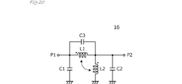
- FIG. 1 is a circuit diagram of a phase shifter 11 according to the first embodiment.
- 2A and 2B are various equivalent circuit diagrams of the transformer T.
- FIG. FIG. 3 is a diagram illustrating a configuration of an antenna circuit including the phase shifter 11 and the antenna 1.
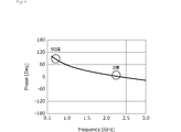
- FIG. 4 is a diagram illustrating frequency characteristics of the phase shift amount of the phase shifter 11 according to the first embodiment.
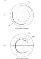
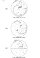
- 5 (A) and 5 (B) are diagrams showing the phase shift action by the phase shifter 11 shown in FIG.
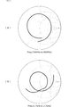
- FIG. 6A shows a low-band locus of impedance Zm viewed from Pm in FIG. 3, and
- FIG. 6B shows a high-band locus of impedance Zm.
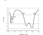
- FIG. 7 is a diagram showing the frequency characteristic of reflection loss viewed from Pm in FIG. FIG.
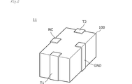
- FIG. 8 is an external perspective view of the phase shifter 11.
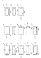
- FIG. 9 is a plan view of each layer of the phase shifter 11.
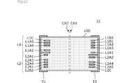
- FIG. 10 is a cross-sectional view of the phase shifter 11.
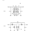
- FIG. 11A is a circuit diagram of the phase shifter 11 of the present embodiment.
- FIG. 11B is an equivalent circuit diagram in which the phase shifter 11 is divided into an ideal transformer IT and a parasitic inductance.
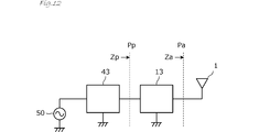
- FIG. 12 is a diagram illustrating a configuration of an antenna circuit including the phase shifter 13 and the antenna 1 according to the third embodiment.
- FIG. 13 is a diagram illustrating the frequency characteristics of the phase shift amount of the phase shifter 13 according to the third embodiment.
- 14 (A) and 14 (B) are diagrams showing the phase shift action by the phase shifter 13 having the characteristics shown in FIG. FIG.
- FIG. 15 is a plan view of each layer of the phase shifter 13 according to the third embodiment.
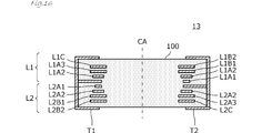
- FIG. 16 is a cross-sectional view of the phase shifter 13.
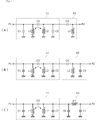
- 17A, 17B, and 17C are circuit diagrams of three phase shifters according to the fourth embodiment.
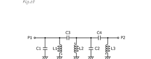
- FIG. 18 is a circuit diagram of another phase shifter according to the present embodiment.
- FIG. 19 is a circuit diagram of the phase shifter 15 according to the fifth embodiment.
- FIG. 20 is a circuit diagram of the phase shifter 16 according to the sixth embodiment.
- FIG. 21 is a block diagram of a communication terminal apparatus 200 according to the seventh embodiment.
- FIG. 22 is a circuit diagram of the phase shifter 18 according to the eighth embodiment.
- FIG. 23 is a diagram illustrating frequency characteristics of the phase shift amount of the phase shifter 18.
- FIG. 24A is a circuit diagram showing a configuration of a diplexer 109 according to the ninth embodiment.
- FIG. 24B is a circuit diagram of a diplexer 109 ⁇ / b> P as a comparative example of the diplexer 109.
- FIG. 25 is a diagram illustrating frequency characteristics of insertion loss between ports Pr2 and Pc depending on the presence or absence of the inductor L11 in the diplexer 109P of the comparative example.
- FIG. 26A is a diagram showing the frequency characteristic of the reflection coefficient at a predetermined port on the Smith chart for the diplexer 109 of the present embodiment.
- FIG. 26B is a diagram showing, on a Smith chart, the frequency characteristics of the reflection coefficient at a predetermined port when the inductor L11 is not provided for the diplexer 109P of the comparative example.
- FIG. 26C is a diagram showing, on a Smith chart, the frequency characteristics of the reflection coefficient at a predetermined port when the inductor L11 is provided for the diplexer 109P of the comparative example.
- FIG. 27A is a diagram illustrating frequency characteristics of insertion loss between the common port Pc and the individual ports Pr1 and Pr2 for the diplexer 109 according to the present embodiment.
- FIG. 27B is a diagram illustrating frequency characteristics of insertion loss between the common port Pc and the individual ports Pr1 and Pr2 when the inductor L11 is not provided for the diplexer 109P of the comparative example.
- FIG. 27C is a diagram illustrating frequency characteristics of insertion loss between the common port Pc and the individual ports Pr1 and Pr2 when the inductor L11 is provided for the diplexer 109P of the comparative example.
- FIG. 28 is a circuit diagram showing a configuration of the multiplexer 110 according to the tenth embodiment.
- FIG. 29 is a diagram showing a frequency characteristic of a reflection coefficient viewed from one port of a general SAW filter on a Smith chart.
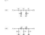
- FIG. 30A is a circuit diagram of a high-pass filter type phase shifter, and FIG.
- FIG. 30B is a circuit diagram of a low-pass filter type phase shifter.
- FIG. 31 shows an example of the phase frequency characteristics of the high-pass filter type phase shifter shown in FIG.
- FIG. 32 shows an example of the phase frequency characteristics of the low-pass filter type phase shifter shown in FIG.
- FIG. 33 is a characteristic example of phase versus insertion loss of the high-pass filter type phase shifter shown in FIG. It is a figure which shows the structural example of the circuit which performs the impedance matching of the 1st high frequency circuit 71 and the 2nd high frequency circuit 74.
- FIGS. 35A, 35B, 35C, and 35D are diagrams showing the displacement of the impedance trajectory when the matching is attempted by the conventional method without using the phase shifter.
- FIG. 36 is a circuit diagram of a diplexer composed of a high-pass filter HPF and a low-pass filter LPF.
- FIG. 1 is a circuit diagram of a phase shifter 11 according to the first embodiment.
- the phase shifter 11 includes a transformer T.
- the transformer T has a first coil L1 and a second coil L2 that is magnetically coupled to the first coil L1 with a coupling coefficient of less than 1.
- the phase shifter 11 includes an impedance adjustment circuit including a first capacitance element C1, a second capacitance element C2, and a third capacitance element C3.
- the first capacitance element C1 is connected in parallel to the first coil L1
- the second capacitance element C2 is connected in parallel to the second coil L2.
- the third capacitance element C3 is connected between the first coil L1 and the second coil L2.
- FIG. 2A and 2B are various equivalent circuit diagrams of the transformer T.
- FIG. The equivalent circuit of the transformer T can be expressed in several forms. 2A, the ideal transformer IT, a series parasitic inductance component La connected in series (series connection) to the primary side thereof, and a parallel parasitic inductance component connected to the primary side in a shunt connection (parallel connection). Lb and a serial parasitic inductance component Lc connected in series (connected in series) to the secondary side.
- the ideal transformer IT two series parasitic inductance components La and Lc1 connected in series (series connection) to the primary side thereof, and a shunt connection (parallel connection) to the primary side. It is represented by a parallel parasitic inductance component Lb.
- the transformer ratio of the transformer T is 1: n
- the coupling coefficient between the first coil L1 and the second coil L2 is k
- the inductance of the first coil L1 is L1
- the inductance of the second coil L2 is Expressed respectively by L2
- the inductances of the parasitic inductance components La, Lb, Lc, and Lc1 have the following relationship.
- the transformer ratio of the ideal transformer is a transformer ratio according to the number of turns of the first coil L1 and the second coil L2.
- the transformer T of the present embodiment generates a series inductance component and a parallel inductance component when the coupling coefficient k between the first coil L1 and the second coil L2 is less than 1.
- FIG. 3 is a diagram showing a configuration of an antenna circuit including the phase shifter 11 and the antenna 1.
- This antenna circuit includes impedance matching circuit units 41 and 42 and a phase shifter 11 between the power feeding circuit 50 and the antenna 1.
- the impedance matching circuit units 41 and 42 and the phase shifter 11 are examples of the “impedance matching circuit unit” according to the present invention.
- the phase shifter 11 shifts the reflected signal from the antenna 1 as viewed from the position indicated by Pa.
- the impedance matching circuit unit 41 constitutes an impedance conversion circuit using a transformer. For example, the impedance Zt viewed from the position indicated by Pt is increased from the impedance Zp viewed from the position indicated by Pp as viewed from the antenna 1 side.
- the impedance matching circuit units 41 and 42 perform impedance matching between the power feeding circuit 50 and the antenna 1.
- FIG. 4 is a diagram showing the frequency characteristics of the phase shift amount of the phase shifter 11 of the present embodiment.
- the phase shift amount is approximately 90 ° in the low band (700 MHz to 900 MHz band), and the phase shift amount is approximately 0 ° in the high band (1.7 GHz to 2.7 GHz band). That is, the present embodiment is an example of a phase shifter that “shifts the low-band signal without shifting the phase of the high-band signal”.
- FIG. 5 (A) and FIG. 5 (B) are diagrams showing the phase shift action by the phase shifter 11 shown in FIG.
- the locus LBa in FIG. 5A is a low-band locus of the impedance Za shown in FIG. 3, and the locus LBp is a low-band locus of the impedance Zp shown in FIG.
- the locus HBa in FIG. 5B is a high-band locus of the impedance Za
- the locus HBp is a high-band locus of the impedance Zp.
- the phase shifter 11 is phase shifted by approximately 90 ° in the low band
- the reflected signal at the position indicated by Pp in FIG. 3 is clockwise by approximately 180 ° from the reflected signal at the position indicated by Pa. Rotate to.
- the impedance locus rotates clockwise by about 180 ° as shown in FIG. Since the phase is hardly shifted in the high band, the reflected signal viewed from Pp is almost the same as the reflected signal viewed from Pa as shown in FIG.
- the main part (most part) of the impedance locus is moved to the second quadrant or the third quadrant on the Smith chart.
- the “second quadrant on the Smith chart” is an area in which the real part of the reflection coefficient is negative and the imaginary part is positive, and is an upper left area obtained by dividing the Smith chart into four crosses.
- the “third quadrant on the Smith chart” is a region where the real part of the reflection coefficient is negative and the imaginary part is negative, and is a lower left region obtained by dividing the Smith chart into four crosses.
- the impedance matching circuit unit 41 increases the impedance with a predetermined impedance conversion ratio as viewed from the input side. Therefore, the impedance matching circuit unit 41 has an effect of making the impedance locus on the Smith chart smaller and shifting it to the right.
- FIG. 6A is a low-band locus of impedance Zm viewed from Pm in FIG. 3, and FIG. 6B is a high-band locus of impedance Zm.
- FIG. 7 is a frequency characteristic diagram of reflection loss viewed from Pm in FIG.
- both the low band and the high band the impedance is moved to the second quadrant or the third quadrant on the Smith chart, and then is moved toward the center on the Smith chart by the impedance matching circuit units 41 and 42.
- both the low band and the high band are impedance matched.
- the impedance matching circuit unit 42 mainly changes the high-band impedance by the shunt-connected (parallel-connected) capacitor and the series-connected (series-connected) inductor, and mainly reduces the low-band by the series-connected capacitor and the shunt-connected inductor. Change the impedance.
- FIGS. 35 A), (B), (C), and (D).
- the locus LBa in FIGS. 35A and 35C is a low band locus of the impedance Za shown in FIG. 3, and the locus HBa in FIGS. 35B and 35D is a high band of the impedance Za shown in FIG. The trajectory.
- the locus LBb in FIG. 35A is a low-band locus when a shunt-connected inductor is provided
- the locus HBb in FIG. 35B is a low-band locus when a shunt-connected inductor is provided. It is a trajectory.
- the locus LBb in FIG. 35C is a low-band locus when a shunt-connected capacitor is provided
- the locus HBb in FIG. 35D is a high-band locus when a shunt-connected capacitor is provided. It is.
- both the low band and the high band are matched as shown in FIGS.
- Second Embodiment a specific configuration example inside the phase shifter 11 is shown.
- FIG. 8 is an external perspective view of the phase shifter 11, and FIG. 9 is a plan view of each layer of the phase shifter 11.
- FIG. 10 is a cross-sectional view of the phase shifter 11.
- the phase shifter 11 includes a plurality of insulating base materials S1 to S13.
- Various conductor patterns are formed on the base materials S1 to S13.
- the “various conductor patterns” include not only conductor patterns formed on the surface of the substrate but also interlayer connection conductors.
- the interlayer connection conductor includes not only a via conductor but also an end face electrode formed on the end face of the multilayer body 100.
- the upper surface of the substrate S1 corresponds to the mounting surface (lower surface) of the laminate 100.
- a terminal T1 as the first port P1 a terminal T2 as the second port P2, a ground terminal GND, and an empty terminal NC are formed.
- Conductors L1A1, L1A2, L1A3, and L1A4 are respectively formed on the base materials S7, S6, S5, and S4.
- Conductors L1A5 and L1B1 are formed on the base material S3.
- Conductors L1B2 and L1C are formed on the base material S2.
- the first end of the conductor L1A1 is connected to the terminal T1 of the first port.
- the second end of the conductor L1A1 is connected to the first end of the conductor L1A2 via the via conductor V1.
- the second end of the conductor L1A2 is connected to the first end of the conductor L1A3 via the via conductor V2.
- the second end of the conductor L1A3 is connected to the first end of the conductor L1A4 via the via conductor V3.
- the second end of the conductor L1A4 is connected to the first end of the conductor L1A5 via the via conductor V4.
- the second end of the conductor L1A5 is connected to the first end of the conductor L1B1.
- the second end of the conductor L1A5 and the first end of the conductor L1B1 are connected to the first end of the conductor L1B2 via the via conductor V6.
- the second end of the conductor L1B1 is connected to the second end of the conductor L1B2 via the via conductor V5.
- the second end of the conductor L1B2 is connected to the first end of the conductor L1C.
- the second end of the conductor L1C is connected to the ground terminal GND.
- Conductors L2A1, L2A2, L2A3, and L2A4 are respectively formed on the base materials S8, S9, S10, and S11.
- Conductors L2A5 and L2B1 are formed on the base material S12.
- Conductors L2B2 and L2C are formed on the base material S13.
- the first end of the conductor L2A1 is connected to the terminal T2 of the second port.
- the second end of the conductor L2A1 is connected to the first end of the conductor L2A2 via the via conductor V7.
- the second end of the conductor L2A2 is connected to the first end of the conductor L2A3 via the via conductor V8.
- the second end of the conductor L2A3 is connected to the first end of the conductor L2A4 via the via conductor V9.
- the second end of the conductor L2A4 is connected to the first end of the conductor L2A5 via the via conductor V10.
- the second end of the conductor L2A5 is connected to the first end of the conductor L2B1.
- the second end of the conductor L2A5 and the first end of the conductor L2B1 are connected to the first end of the conductor L2B2 via the via conductor V12.
- the second end of the conductor L2B1 is connected to the second end of the conductor L2B2 via the via conductor V11.
- the second end of the conductor L2B2 is connected to the first end of the conductor L2C.
- the second end of the conductor L2C is connected to the ground terminal GND.
- the first coil L1 is configured by V6.
- the conductors L2A1, L2A2, L2A3, L2A4, L2A5, L2B1, L2B2, L2C and the via conductors V7, V8, V9, V10, V11, V12 constitute a second coil L2.
- Both the first coil L1 and the second coil L2 are rectangular helical coils.
- Each base material layer of the laminate 100 may be a non-magnetic ceramic laminate composed of LTCC (Low Temperature Co-fired Ceramics) or a resin material such as polyimide or liquid crystal polymer. It may be a resin laminate.
- LTCC Low Temperature Co-fired Ceramics
- resin material such as polyimide or liquid crystal polymer. It may be a resin laminate.
- the base material layer is a non-magnetic material (because it is not a magnetic material ferrite), it can be used as a transformer and a phase shifter having a predetermined inductance and a predetermined coupling coefficient even in a high frequency band exceeding several hundred MHz.
- the conductor pattern and the interlayer connection conductor are made of a conductor material having a small specific resistance mainly composed of Ag or Cu. If the base material layer is ceramic, for example, it is formed by screen printing and baking of a conductive paste mainly composed of Ag or Cu. Moreover, if a base material layer is resin, metal foil, such as Al foil and Cu foil, will be formed by patterning by an etching etc., for example.
- the first coil L1 and the second coil L2 have substantially the same inner and outer diameters and the coil winding axis CA is substantially the same (coaxial)
- the first coil The winding axis CA1 of L1 and the winding axis CA2 of the second coil L2 are deliberately shifted slightly.
- each conductor formed on each base material forms a substantially rectangular loop, but is formed on each of the base materials S5, S4, S3, and S2.
- the line widths of the upper side and the right side of the loop are narrower than the line widths of the lower side and the left side.
- the winding axis CA1 see FIG.
- each conductor formed on each of the base materials S10, S11, S12, and S13 has a line width of the lower side and the left side of the loop made thinner than that of the upper side and the right side.
- the winding axis CA2 (see FIG. 10) of the second coil L2 is slightly shifted to the lower left from the center of the loop outer shape. This intentionally keeps the coupling coefficient between the first coil L1 and the second coil L2 low.
- the interlayer distance between the main part of the first coil L1 excluding the conductor L1A1 and the main part of the second coil L2 excluding the conductor L2A1 is increased. This also intentionally suppresses the coupling coefficient between the first coil L1 and the second coil L2.
- FIG. 11A is a circuit diagram of the phase shifter 11 of the present embodiment.
- the first coil L1 and the second coil L2 constitute a transformer.
- the first capacitance element C1 is mainly composed of a capacitance generated between conductor layers formed on the base materials S2, S3, S4, S5, S6 and S7.
- the second capacitance element C2 is mainly composed of a capacitance generated between conductor layers formed on the base materials S8, S9, S10, S11, S12, and S13.
- the third capacitance element C3 is an inter-coil capacitance mainly generated between the first coil L1 and the second coil L2, and is mainly configured by a capacitance generated mainly between the conductor L1A1 and the conductor L2A1. .
- the capacitance of the third capacitance element C3 is increased by arranging the conductor L1A1 and the conductor L2A1 so as to be adjacent to each other in the stacking direction.
- first coil L1 and the second coil L2 are symmetrical in the stacking direction and have the same number of turns, they function as a transformer having an impedance conversion ratio of 1: 1.
- FIG. 11B is an equivalent circuit diagram in which the phase shifter 11 is divided into an ideal transformer IT and parasitic inductance components (series parasitic inductance components La and Lc, parallel parasitic inductance component Lb).
- the parasitic inductance components cause the transformer inductance to deviate from a specified value (for example, 50 ⁇ ).
- a specified value for example, 50 ⁇
- the capacitance elements C1, C2, and C3 act to correct the impedance deviation due to the parallel parasitic inductance component Lb
- the capacitance element C3 acts to correct the impedance deviation due to the series parasitic inductance components La and Lc.
- the capacitance elements C1, C2, and C3 are examples of the “reactance element that suppresses the impedance shift due to the parasitic inductance component” according to the present invention.
- the series parasitic inductance component Lc is large as the coupling coefficient between the first coil L1 and the second coil L2 is small.
- impedance matching is ensured by the large capacitance of the third capacitance element C3.
- the capacitance of the third capacitance element C3 is large, the ratio of the high-band signal passing through the third capacitance element C3 is larger than the transformer formed by the first coil L1 and the second coil L2, and the phase shift by the transformer is performed. Little effect occurs. This is as shown in FIG. 5B in the first embodiment.
- the amount of bypassing the third capacitance element C3 is relatively small, and the phase shift action by the transformer is effective.
- the coupling coefficient k between the first coil L1 and the second coil L2 is small, the amount of phase shift is less than 180 °.
- the coupling coefficient k is set to be small so that the amount of phase shift with respect to the low band signal is approximately 90 °.
- the ratio of the parallel connection portions of the conductors L1B1 and L1B2 occupying the first coil L1 shown in FIG. 11A is determined by the positions of the via conductors V5 and V6 shown in FIG.
- the ratio of the parallel connection portions of the conductors L2B1 and L2B2 in the second coil L2 shown in FIG. 11A is determined by the positions of the via conductors V11 and V12 shown in FIG. Therefore, the inductance of the first coil L1 can be finely adjusted by the positions of the via conductors V5 and V6, and the inductance of the second coil L2 can be finely adjusted by the positions of the via conductors V11 and V12.
- the current flows in a distributed manner in the parallel connection portions of the conductors L1B1 and L1B2, whereas the conductor L1A1 does not have such a current distribution.
- current flows through the parallel connection portions of the conductors L2B1 and L2B2, whereas the conductor L2A1 does not have such current distribution.
- the conductor portions close to each other in the stacking direction contribute most to the coupling. That is, the portions of the conductors L1A1 and L2A1 that are opposed in the stacking direction over the entire circumference contribute to the coupling of the first coil L1 and the second coil L2. As described above, the conductor L1A1 and L2A1 have no current distribution due to the parallel connection portion, and thus the coupling coefficient between the first coil L1 and the second coil L2 is high.
- the conductors L1A1 and L2A1 connected to the terminals T1 and T2 are arranged near the center in the stacking direction, and the conductors L1C and L2C to which the ground terminal GND is connected are arranged above and below in the stacking direction.
- the transformer in which the first coil L1 and the second coil L2 share the magnetic flux can be configured, and the adjustment of the capacitance element C3 is facilitated.
- the parallel connection portion is provided in a position close to the conductor pattern of the counterpart coil in the stacking direction. You may utilize the effect
- the coupling coefficient k between the first coil L1 and the second coil L2 is decreased and the third capacitance element C3 is increased, so that the high-band signal is almost the third capacitance element C3.
- the amount of phase shift by the transformer was suppressed by reducing the coupling coefficient k between the first coil L1 and the second coil L2. With these configurations, the phase is shifted by 90 ° in the low band and is hardly shifted in the high band.
- the above configuration is an example.
- the amount of phase shift according to the frequency band can be determined by the coupling coefficient k and the capacitance of the third capacitance element C3.
- the phase shift amount in the low band is about 90 ° and the phase shift amount in the high band is about 0 °. There is a width. If the phase shift amount in the low band is closer to 90 ° than 0 °, and the phase shift amount in the high band is closer to 0 ° than 90 °, the first, first, The operational effects shown in the second embodiment are similarly obtained.
- the third embodiment is an example of a phase shifter that “shifts the high-band signal without shifting the low-band signal”.
- the circuit diagram of the phase shifter is the same as that shown in FIG. 1 in the first embodiment.
- FIG. 12 is a diagram showing a configuration of an antenna circuit including the phase shifter 13 and the antenna 1 according to the third embodiment.
- This antenna circuit includes an impedance matching circuit unit 43 and a phase shifter 13 between the power feeding circuit 50 and the antenna 1.
- the phase shifter 13 shifts the reflected signal from the antenna 1 as viewed from Zp.
- the impedance matching circuit unit 43 performs impedance matching between the power feeding circuit 50 and the antenna 1 together with the phase shifter 13.
- FIG. 13 is a diagram showing the frequency characteristics of the phase shift amount of the phase shifter 13 according to the third embodiment.
- the phase shift amount is approximately 180 ° in the low band (700 MHz to 900 MHz band), and the phase shift amount is approximately 90 ° in the high band (1.7 GHz to 2.7 GHz band).
- the locus LBa in FIG. 14A is the locus of the impedance Za in the low band as viewed from Pa in FIG. 12, and the locus LBp is the locus of the impedance Zp in the low band as viewed from Pp in FIG.
- the locus HBa in FIG. 14B is the locus of the impedance Za in the high band as viewed from Pa in FIG. 12, and the locus HBp is the locus of the impedance Zp in the high band as viewed from Pp in FIG. is there.
- the coupling coefficient k between the first coil L1 and the second coil L2 is deliberately reduced to reduce the amount of phase shift due to the transformer structure.
- the first coil The coupling coefficient k between L1 and the second coil L2 is as close as possible to 1, and the phase shift amount due to the transformer structure is close to 180 °.
- the phase shifter of the present embodiment has a phase shift of approximately 180 ° in the low band (a phase shift of approximately 360 ° in the reciprocation), so that it is viewed from Pp as shown in FIG.
- the phase of the reflected signal is substantially the same as the phase of the reflected signal viewed from Pa.
- the phase of the reflected signal viewed from Pp rotates clockwise by approximately 180 ° from the phase of the reflected signal viewed from Pa. Further, the circle of the impedance locus is gathered small due to the capacitance component of the second capacitance element C2 (see FIGS. 11A and 11B).
- the impedance matching circuit unit 43 shown in FIG. 12 includes a series-connected reactance element and a shunt-connected reactance element, and matches the impedance in the state shown in FIGS.
- phase shifter 13 of this embodiment is the same as that shown in FIG. 8 in the second embodiment.
- FIG. 15 is a plan view of each layer of the phase shifter 13 of the present embodiment.
- FIG. 16 is a sectional view of the phase shifter 13.
- the circuit diagram of the phase shifter 13 is the same as FIG. 11A shown in the second embodiment.
- the phase shifter 13 includes a plurality of insulating base materials S1 to S9. Various conductor patterns are formed on the base materials S1 to S9.
- the “various conductor patterns” include not only conductor patterns formed on the surface of the substrate but also interlayer connection conductors.
- the interlayer connection conductor includes not only a via conductor but also an end face electrode formed on the end face of the multilayer body.
- the upper surface of the substrate S1 corresponds to the mounting surface (lower surface) of the laminate.
- a terminal T1 as the first port P1 a terminal T2 as the second port P2, a ground terminal GND, and an empty terminal NC are formed.
- Conductors L1A1 and L1A2 are formed on the base materials S5 and S4, respectively.
- Conductors L1A3 and L1B1 are formed on the base material S3.
- Conductors L1B2 and L1C are formed on the base material S2.
- the first end of the conductor L1A1 is connected to the terminal T1 of the first port.
- the second end of the conductor L1A1 is connected to the first end of the conductor L1A2 via the via conductor V1.
- the second end of the conductor L1A2 is connected to the first end of the conductor L1A3 via the via conductor V2.
- the second end of the conductor L1A3 is connected to the first end of the conductor L1B1.
- the second end of the conductor L1A3 and the first end of the conductor L1B1 are connected to the first end of the conductor L1B2 via the via conductor V3.
- the second end of the conductor L1B1 is connected to the second end of the conductor L1B2 via the via conductor V4.
- the second end of the conductor L1B2 is connected to the first end of the conductor L1C.
- the second end of the conductor L1C is connected to the ground terminal GND.
- Conductors L2A1 and L2A2 are formed on the base materials S6 and S7, respectively.
- Conductors L2A3 and L2B1 are formed on the base material S8.
- Conductors L2B2 and L2C are formed on the base material S9.
- the first end of the conductor L2A1 is connected to the terminal T2 of the second port.
- the second end of the conductor L2A1 is connected to the first end of the conductor L2A2 via the via conductor V5.
- the second end of the conductor L2A2 is connected to the first end of the conductor L2A3 via the via conductor V6.
- the second end of the conductor L2A3 is connected to the first end of the conductor L2B1.
- the second end of the conductor L2A3 and the first end of the conductor L2B1 are connected to the first end of the conductor L2B2 via the via conductor V7.
- the second end of the conductor L2B1 is connected to the second end of the conductor L2B2 via the via conductor V8.
- the second end of the conductor L2B2 is connected to the first end of the conductor L2C.
- the second end of the conductor L2C is connected to the ground terminal GND.
- a first coil L1 is constituted by the conductors L1A1, L1A2, L1A3, L1B1, L1B2, L1C and the via conductors V1, V2, V3, V4.
- the conductor L2A1, L2A2, L2A3, L2B1, L2B2, L2C and the via conductors V5, V6, V7, V8 constitute a second coil L2.
- Both the first coil L1 and the second coil L2 are rectangular helical coils.
- the line widths of the conductors L1A1 and L2A1 formed on the base materials S5 and S6 are narrower than those of other conductors.
- the line widths of the conductors L1A2 and L2A2 formed on the base materials S4 and S7 are narrower than the line width of the conductors formed on the base materials S3 and S8. Therefore, the inter-coil capacitance generated between the first coil L1 and the second coil L2 is small, and the capacitance of the third capacitance element C3 is kept small.
- line width is so thin that it is a conductor pattern which mutually adjoins among the multiple-layer conductor pattern which comprises the 1st coil L1, and the multiple-layer conductor pattern which comprises the 2nd coil L2, The farther away, the thicker the line width.
- the first coil L1 and the second coil L2 have substantially the same inner and outer diameters, and the coil winding axis CA has the same (coaxial) relationship.
- the interlayer distance between the formation layers of the first coil L1 and the second coil L2 is short. Therefore, a transformer having a high coupling coefficient k between the first coil L1 and the second coil L2 can be obtained.
- phase shift amount in the low band is about 180 ° and the phase shift amount in the high band is about 90 °.
- the phase shift amount in the low band is closer to 180 ° than 90 °
- the phase shift amount in the high band is closer to 90 ° than 180 °. Has the function and effect.
- a phase shifter including a high-pass filter or a low-pass filter is shown.
- FIG. 17A, 17B, and 17C are circuit diagrams of three phase shifters according to the fourth embodiment.
- a high-pass filter 61 is connected in series to the phase shifter 11.
- the high-pass filter 61 includes a series-connected capacitance element C4 and a shunt-connected inductance element.
- a high pass filter 62 is connected in series to the phase shifter 11.
- the high-pass filter 62 includes a series-connected capacitance element C4, a parallel-connected inductance element L3, and a capacitance element C5.
- a low-pass filter 63 is connected in series to the phase shifter 11.
- the low-pass filter 63 includes a series-connected inductance element L4 and parallel-connected capacitance elements C6 and C7.
- phase shifter 11 By connecting a high-pass filter or a low-pass filter in series to the phase shifter 11 as in this embodiment, when the phase shifter 11 alone does not satisfy the predetermined phase shift amount, the insufficient phase shift amount is highpassed. It can be supplemented by a filter or a low-pass filter, and a phase shifter with a predetermined phase shift amount can be configured.
- phase shift amount is increased by 5 ° by the added high-pass filter as shown in FIG. .
- the phase shift amount is adjusted by a shunt-connected capacitance element C5 as shown in FIG.
- a low-pass filter is added as shown in FIG.
- the inductance element and the capacitance element may be individual parts or may be formed by a conductor pattern. Furthermore, it may be formed integrally with the phase shifter 11.
- the inductance elements L3 and L4 in the filter are integrally provided in the phase shifter 11, whereby the inductance elements L3 and L4 are connected to the first coil L1. And it may be magnetically coupled to the second coil L2.
- the amount of phase shift due to the addition of the high-pass filters 61 and 62 can be made different from that in the case where there is no coupling.
- the frequency characteristics of the amount of phase shift due to the addition of the low-pass filter 63 can be made different from the case where there is no coupling.
- FIG. 18 is a circuit diagram of another phase shifter according to the present embodiment.
- the basic configuration is the same as that of the circuit shown in FIG. 17A, but the polarity of coupling of the inductance element L3 to the first coil L1 and the second coil L2 is opposite to that of the circuit shown in FIG. .
- the increase / decrease in the amount of phase shift due to the addition of the high-pass filter 61 can also be adjusted by the polarity of this coupling.
- the increase and decrease in the amount of phase shift due to the addition of the high-pass filter 62 and the low-pass filter 63 can be adjusted by the polarity of coupling of the inductance elements L3 and L4.
- FIG. 19 is a circuit diagram of the phase shifter 15 according to the fifth embodiment.
- the phase shifter using a transformer having an impedance conversion ratio of 1: 1 is shown in the examples shown in FIGS. 1, 2A, 2B, etc., but the impedance conversion ratio is 1: n. (N is a value other than 1).
- N is a value other than 1).
- impedance matching can be performed together with a predetermined phase shift.
- FIG. 20 is a circuit diagram of the phase shifter 16 according to the sixth embodiment.
- the phase shifter 16 of the present embodiment includes an auto-transformer transformer that includes a first coil L1 and a second coil L2 that are magnetically coupled to each other.
- a first capacitance element C1 is connected between the first port P1 and the ground, and a second capacitance element C2 is connected between the second port P2 and the ground.
- a third capacitance element C3 is connected between the first port P1 and the second port P2.
- a parallel inductance component and a series inductance component are also generated in the autotransformer transformer because the coupling coefficient between the first coil L1 and the second coil L2 is less than 1.
- the impedances are matched by the capacitance elements C1, C2, and C3.
- FIG. 21 is a block diagram of a communication terminal apparatus 200 according to the seventh embodiment.
- the communication terminal device 200 includes an antenna 1, an antenna matching circuit 40, a phase shift circuit 30, a communication circuit 51, a baseband circuit 52, an application processor 53, and an input / output circuit 54.
- the communication circuit 51 includes a transmission circuit and a reception circuit for a low band (700 MHz to 1.0 GHz) and a high band (1.4 GHz to 2.7 GHz), and an antenna duplexer.
- the antenna 1 is a monopole antenna, an inverted L antenna, an inverted F antenna, or the like corresponding to a low band and a high band.
- the above components are housed in one housing.
- the antenna matching circuit 40, the phase shift circuit 30, the communication circuit 51, the baseband circuit 52, and the application processor 53 are mounted on a printed wiring board, and the printed wiring board is housed in a housing.
- the input / output circuit 54 is incorporated in the housing as a display / touch panel.
- the antenna 1 is mounted on a printed wiring board or disposed on the inner surface or inside of the housing.
- a phase shifter having a frequency characteristic in the amount of phase shift will be described.
- a phase shift of 180 ° is performed by a transformer, but the transformer does not have a frequency characteristic in the amount of phase shift. Therefore, it is difficult to obtain a predetermined phase shift amount in a specific frequency band that is only a transformer, or to obtain a predetermined phase shift amount corresponding to the frequency over a certain frequency range.
- FIG. 22 is a circuit diagram of the phase shifter 18 according to the eighth embodiment. It differs from the phase shifter 11 shown in FIG. 1 in 1st Embodiment by the point provided with the inductance element L5. That is, a series circuit SR of the third capacitance element C3 and the inductance element L5 is provided between the first port P1 and the second port P2 of the transformer T. Other basic configurations are the same as those of the phase shifter 11 of the first embodiment.
- the phase shifter 18 of the present embodiment can be a low-pass filter.
- Part LPF and high-pass filter part HPF the first capacitance element C1, the second capacitance element C2, and the inductance element L5 constitute a low-pass filter portion LPF
- the first coil L1, the second coil L2, and the third capacitance element C3 constitute a high-pass filter portion HPF.
- the high-pass filter HPF is constituted by the parallel parasitic inductance component of the transformer T (see Lb in FIGS. 2A and 2B) by the first coil L1 and the second coil L2 and the third capacitance element C3. it can.
- FIG. 23 is a diagram showing the frequency characteristics of the phase shifter 18 of this embodiment and the phase shifter of the comparative example.
- the inductance element L5 is not provided in FIG. 22, and the third capacitance element C3 is provided in the bypass path.
- the curve PS (LC) represents the frequency characteristic of the phase shifter 18
- the curve PS (C) represents the frequency characteristic of the phase shifter of the comparative example.
- the comparative phase shifter acts as a transformer phase shifter in a low frequency band. In the high frequency band, the amount that the signal bypasses the third capacitance element C3 increases, and the phase shift amount gradually approaches 0 °.
- the amount of phase shift is negative in the high range.
- the operation of the phase shifter 18 of the present embodiment is divided into three frequency bands F1, F2, and F3.
- the capacitance of the third capacitance element C3 is dominant in the LC series circuit SR. Therefore, the signal propagating between the ports P1 and P2 hardly bypasses the LC series circuit SR. That is, the characteristics of the transformer T appear.
- the bypass circuit acts as a high-pass filter, and the amount of phase shift decreases as the frequency increases.
- the bypass circuit acts as a low-pass filter and has a negative phase shift amount.
- the frequency at which the phase shift amount is 0 ° corresponds to the series resonance frequency of the LC series circuit SR.
- the frequency characteristic of the amount of phase shift is determined by the parallel parasitic inductance components of the first capacitance element C1, the second capacitance element C2, the third capacitance element C3, the inductance element L5, and the transformer T.
- a predetermined large frequency characteristic can be given to the amount of phase shift. Further, a predetermined phase shift amount corresponding to the frequency can be obtained over a wide frequency band.
- the first capacitance element C1, the second capacitance element C2, the third capacitance element C3, and the inductance element L5 not only define the frequency characteristics of the phase shift amount, but also have a predetermined impedance (generally 50 ⁇ ). It also acts as an element for matching.
- a diplexer including a phase shifter together with a high-pass filter and a low-pass filter is shown.
- This diplexer is an example of the “multiplexer / demultiplexer” according to the present invention.
- FIG. 24A is a circuit diagram showing a configuration of a diplexer 109 according to the ninth embodiment.
- the diplexer 109 includes a high band pass high pass filter HPF and a low band pass low pass filter LPF connected between the common port Pc and the individual ports Pr1 and Pr2.
- the antenna 1 is connected to the common port Pc.
- the high-pass filter HPF includes a first inductor L11 that is shunt-connected between the signal line and the ground, and a first capacitor C11 that is connected in series to the line after the first inductor L11.
- a first inductor L13 that is connected in parallel to the first capacitor C11 is provided, and an inductor L12 that is shunt-connected in the subsequent stage is further provided.
- the low-pass filter LPF includes a second inductor L21 connected in series to the common port Pc, and a second capacitor C21 connected in shunt between the ground after the second inductor L21.
- the present embodiment further includes a capacitor C22 connected in parallel to the second inductor L21, and further includes a parallel connection circuit of the inductor L22 and the capacitor C23 connected in series at the subsequent stage of the shunt-connected second capacitor C21.
- a phase shifter 19 is inserted between the common port Pc and the first inductor L11.
- the phase shifter 19 shifts the phase so that the high pass filter HPF is substantially open (equivalent) in the pass frequency band (low band) of the low pass LPF as viewed from the common port Pc.
- FIG. 24B is a circuit diagram of a diplexer 109P as a comparative example of the diplexer 109. Unlike the diplexer 109, the phase shifter 19 is not provided.
- FIG. 25 is a diagram showing frequency characteristics of insertion loss between ports Pr2 and Pc depending on the presence or absence of the inductor L11 in the diplexer 109P of the comparative example.
- the characteristic curve C is a characteristic when the inductor L11 is provided
- N is a characteristic when the inductor L11 is not provided.
- FIG. 26A is a diagram showing the frequency characteristics of the reflection coefficient at a predetermined port on the Smith chart for the diplexer 109 of the present embodiment.
- FIG. 26B is a diagram showing, on a Smith chart, the frequency characteristics of the reflection coefficient at a predetermined port when the inductor L11 is not provided for the diplexer 109P of the comparative example.
- FIG. 26C is a diagram showing, on a Smith chart, the frequency characteristics of the reflection coefficient at a predetermined port when the inductor L11 is provided for the diplexer 109P of the comparative example.
- curve A represents the characteristic viewed from the common port Pc
- curve F represents the characteristic viewed from the individual port Pr1.
- the diplexer 109 when viewed from the common port Pc, the diplexer 109 is substantially open in the low band (960 MHz), and the high band (1 .7 GHz) to match the specified impedance (50 ⁇ ). Further, when viewed from the individual port Pr1, it matches with the specified impedance (50 ⁇ ) in the high band (1.7 GHz).
- FIG. 27A is a diagram showing the frequency characteristics of insertion loss between the common port Pc and the individual ports Pr1 and Pr2 for the diplexer 109 of the present embodiment.
- FIG. 27B is a diagram illustrating frequency characteristics of insertion loss between the common port Pc and the individual ports Pr1 and Pr2 when the inductor L11 is not provided for the diplexer 109P of the comparative example.
- FIG. 27C is a diagram illustrating frequency characteristics of insertion loss between the common port Pc and the individual ports Pr1 and Pr2 when the inductor L11 is provided for the diplexer 109P of the comparative example.
- the curve LPF represents the characteristics of the low-pass filter LPF
- the curve HPF represents the characteristics of the low-pass filter HPF
- the curve ISO represents the inter-port isolation characteristic.
- the low-pass filter LPF has a low-band insertion loss of ⁇ 1 dB or less, and a high-band (1.7 GHz to 2.7 GHz or less) attenuation is ⁇ 30 dB or more. is there.
- the high-pass filter HPF has an insertion loss in the high band of ⁇ 1 dB or less and an attenuation in the low band of ⁇ 28 dB or more.
- the tenth embodiment shows a multiplexer including a plurality of SAW filters and a phase shifter together with these SAW filters.
- This multiplexer is an example of the “multiplexer / demultiplexer” according to the present invention.
- FIG. 28 is a circuit diagram showing a configuration of the multiplexer 110 according to the tenth embodiment.
- the multiplexer 110 includes phase shifters 19a, 19b, 19c, 19d and SAW filters SAWa, SAWb, SAWc, SAWd connected between the common port Pc and the individual ports Pr1, Pr2, Pr3, Pr4, respectively.
- the phase shifters 19a, 19b, 19c, and 19d are transformer type phase shifters already shown in some embodiments.
- an antenna is connected to the common port Pc, and a communication circuit for each frequency band is connected to the individual ports Pr1, Pr2, Pr3, and Pr4.
- Each SAW filter SAWa, SAWb, SAWc, SAWd has a first port and a second port, respectively, and the passing frequency bands are different from each other.
- the first SAW filter SAWa has a first port connected to the common port Pc via the phase shifter 19a, and a second port connected to the individual port Pr1.
- the second SAW filter SAWb has the first port connected to the common port Pc via the phase shifter 19b, the second port connected to the individual port Pr2, and the third SAW filter SAWc has the first port phase-shifted.
- the second port is connected to the individual port Pr3 via the phase shifter 19c, the first port is connected to the common port Pc via the phase shifter 19d, and the second port is connected to the individual port Pr3.
- the center frequency of the pass band of the first SAW filter SAWa is 700 MHz
- the center frequency of the pass band of the second SAW filter SAWb is 800 MHz
- the center frequency of the pass band of the third SAW filter SAWc is 900 MHz
- the center frequency of the pass band of the fourth SAW filter SAWd is 2 GHz. That is, the SAW filters SAWa, SAWb, and SAWc are for the low band, and the SAW filter SAWd is for the high band.
- the phase shifter 19a performs phase shifting so that the first SAW filter SAW is substantially open in the pass frequency band of the SAW filters SAWb, SAWc, and SAWd other than the first SAW filter SAWa as viewed from the common port Pc.
- the phase shifter 19b shifts the phase so that the second SAW filter SAWb is substantially open in the pass frequency band of the SAW filters SAWa, SAWc, and SAWd other than the second SAW filter SAWb as viewed from the common port Pc. .
- the phase shifter 19c performs phase shifting so that the third SAW filter SAWc is substantially open in the pass frequency band of the SAW filters SAWa, SAWb, and SAWd other than the third SAW filter SAWc when viewed from the common port Pc.
- the phase shifter 19d shifts the phase so that the fourth SAW filter SAWd is substantially open in the pass frequency band of the SAW filters SAWa, SAWb, SAWc other than the fourth SAW filter SAWd when viewed from the common port Pc.
- FIG. 29 is a diagram showing a frequency characteristic of a reflection coefficient viewed from one port of a general SAW filter on a Smith chart.
- the impedance In the frequency band lower than the pass band, the impedance is substantially short-circuited, and becomes the specified impedance (50 ⁇ ) at the center frequency fc of the pass frequency band, and in the frequency band higher than the pass band, the impedance becomes substantially short again.
- the SAW filters having a large passing frequency band are mutually shifted by the phase shifter by about 180 °, the SAW filters appear to be open to each other. Therefore, it can be directly connected to the common port Pc via the phase shifter. In this state, isolation between ports is ensured.
- the phase shift amount of the phase shifters 19a to 19d is not limited to 180 °, and may be set to an appropriate phase shift amount according to the frequency band.
- a transformer type phase shifter having a frequency characteristic in the amount of phase shift shown in the second embodiment or the eighth embodiment may be used.
- each of the phase shifters 19a to 19d shown in FIG. 28 is configured by a conventional high-pass filter type phase shifter
- the gradient of the frequency characteristic due to the characteristics of L and C is large (the frequency characteristic is large). . Therefore, since a predetermined amount of phase shift can be obtained only in a narrow band, isolation between ports cannot be ensured over a wide band. For this reason, conventionally, when a plurality of SAW filters having a large frequency band are used, a circuit that separates high-band and low-band signals with a diplexer and switches the plurality of SAW filters with a switch within each band is configured. It was.
- the phase adjustment according to the present invention is a mechanism using a transformer, a change in the amount of phase shift with respect to a frequency change is small as compared with a high-pass filter type, a low-pass filter type, or a line type phase adjustment mechanism. Therefore, the frequency at which the phase can be inverted to the open side has a wider band than before, and it is possible to connect the SAW filter in a wider band.
- the phase is approximately 0 degrees in the pass band of the SAW filter, and the phase is -180 degrees in the high frequency band.
- signals that are far apart in the frequency band can be multiplexed and demultiplexed while maintaining isolation between ports.
- an impedance adjustment circuit for adjusting the impedance of a transformer is configured by three capacitance elements C1, C2, and C3 has been described.
- the impedance adjustment circuit is a circuit for correcting or actively correcting the displacement of the impedance due to the parallel inductance component and the series inductance component, which are parasitic components of the transformer, and thus is not limited to three capacitance elements.
- the impedance of the transformer T may be finely adjusted by connecting predetermined reactance elements to the transformer in parallel or in series.
- the first capacitance element C1 and the second capacitance element C2 are not limited to the line capacitance of the coil, and may be configured by a conductor pattern other than the coil. Further, a capacitor as an external component may be connected. Further, the third capacitance element C3 is not limited to the inter-coil capacitance, and may be configured with a conductor pattern other than the coil. Further, a capacitor as an external component may be connected.
Landscapes
- Physics & Mathematics (AREA)
- Acoustics & Sound (AREA)
- Waveguide Switches, Polarizers, And Phase Shifters (AREA)
- Transmitters (AREA)
- Filters And Equalizers (AREA)
- Surface Acoustic Wave Elements And Circuit Networks Thereof (AREA)
- Input Circuits Of Receivers And Coupling Of Receivers And Audio Equipment (AREA)
Abstract
第1ポート(P1)と第2ポート(P2)との間に接続され、第1コイル(L1)および第1コイル(L1)に対して磁界結合する第2コイル(L2)を有し、寄生インダクタンス成分を含むトランス(T)と、前記トランスの寄生インダクタンス成分によるインピーダンスのずれを抑制するリアクタンス素子(C1,C2,C3)を有するインピーダンス調整用回路と、を備える。トランス(T)の第1コイル(L1)と第2コイル(L2)との結合係数およびインピーダンス調整用回路のリアクタンス素子(C1,C2,C3)の値は、周波数帯に応じて異なる移相量となるように定められる。
Description
本発明は、高周波回路に設けられる移相器に関し、特に、周波数帯に応じた移相を行う移相器に関する。また、本発明は、インピーダンス整合回路に関し、特に、移相器を備えるインピーダンス整合回路に関する。また、本発明は、合分波器に関し、特に、移相器を備える合分波器に関する。また、本発明は、上記移相器、インピーダンス整合回路または合分波器を備える通信端末装置に関する。
一般に、高周波回路において、インピーダンス整合のために移相器が用いられることがある。従来、移相器にはハイパスフィルタ型とローパスフィルタ型があり、所望の周波数で所望の移相量を得るように回路定数が定められる。例えば、特許文献1にはハイパスフィルタ型回路とローパスフィルタ型回路を備えた移相器が示されている。
例えば、携帯電話端末をはじめとする通信端末装置等においては、複数の周波数帯域においてインピーダンス整合を図ることが必要となる場合が多い。例えば、図34に示すように、インピーダンス整合回路72と第2高周波回路74との間に移相器73を設け、この移相器73とインピーダンス整合回路72とで、第1高周波回路71と第2高周波回路74とをインピーダンス整合させることを考えると、複数の周波数帯域でインピーダンス整合させるために、移相器には周波数帯に応じた移相特性が要求される。
例えば、ローバンドとハイバンドの両方についてインピーダンス整合を行う際に、一方のバンドの位相をほとんど移相させずに他方のバンドの位相を大きく移相させる必要が生じる場合がある。例えば次の2つの移相操作がある。
(1)ローバンド信号を移相させず、ハイバンド信号を移相させる。
例えば、ローバンド信号の通過位相は0°(または180°)付近であり、ハイバンド信号の通過位相は90°付近である。
(2)ハイバンド信号を移相させず、ローバンド信号を移相させる。
例えば、ローバンド信号の通過位相は90°付近であり、ハイバンド信号の通過位相は0°または180°付近である。
なお、図34において、インピーダンス整合回路72からみて、第2高周波回路74からの反射波は移相器73を往復するので、移相器73での反射信号の移相量は2倍である。すなわち、反射位相を180°とするには、90°の移相量が必要であり、反射位相を0°とするには、0°または180°の移相量が必要である。
ところが、上記(1)(2)に示すような周波数帯域毎の移相操作が可能な移相器は、以下に示すとおり、従来無かった。
例えば、図31は図30(A)に示すハイパスフィルタ型の移相器の位相周波数特性の一例である。この例では、ローバンド(700MHz帯)での移相量は90°にできるが、ハイバンド(2GHz帯)での移相量は0°とはならず30°である。また、図32は図30(B)に示すローパスフィルタ型の移相器の位相周波数特性の一例である。この例では、ローバンド(700MHz帯)での移相量は-90°にできるが、ハイバンド(2GHz帯)での移相量は180°とはならず約100°である。また、ローバンド、ハイバンドのいずれにおいても、周波数帯域内での移相量の変化が大きい。
また、図33は図30(A)に示すハイパスフィルタ型の移相器の位相対挿入損失の特性例である。カットオフ周波数付近で移相量は180°となるため、移相量を大きくしようとすると、挿入損失は大きくなる。また、図30(B)に示すローパスフィルタ型の移相器では、ローバンドで180°付近の移相量を得ようとすると、カットオフ周波数が低くなり、ハイバンドでの挿入損失は非常に大きくなる。
以上のとおり、従来のフィルタ型の移相器では、上記(1)(2)に示すような周波数帯域毎の移相操作が不可能であった。
一方、共通ポートと複数の個別ポートとの間に、それぞれ周波数特性の異なるフィルタが設けられたダイプレクサやマルチプレクサにおいて、通常、各フィルタはそれぞれ単独での特性が得られない。
例えば、図36は、ハイパスフィルタHPFとローパスフィルタLPFとで構成されるダイプレクサの回路図である。この例では、ハイパスフィルタHPFとローパスフィルタLPFとの共通ポートにアンテナANTが接続されている。ハイパスフィルタHPFの個別ポートにはハイバンドの回路が接続され、ローパスフィルタLPFの個別ポートにはローバンドの回路が接続される。ハイパスフィルタHPFは、グランドに対しシャント接続のインダクタL11,L12とシリーズ接続のキャパシタC11とで構成され、ローパスフィルタLPFは、シリーズ接続のインダクタL21,L22とシャント接続のキャパシタC21とで構成される。
ところが、図36に示されるような回路においては、ローバンドの周波数帯で、ハイパスフィルタHPFのインダクタL11のインピーダンスが非常に小さくなると、インダクタL11は実質的にショート素子となり、ローパスフィルタLPFにショート素子(L11)が接続されることになって、ローバンドの周波数帯において、ローバンド回路とハイバンド回路とのアイソレーションが劣化する。
或る使用周波数帯において、他の周波数帯で実質的にショートとなるフィルタが共通ポートに接続されている構成となる場合の上述の問題は、ハイパスフィルタとローパスフィルタの組み合わせによるダイプレクサに限らず、複数のバンドパスフィルタの組み合わせによるマルチプレクサ等についても同様に生じる。
本発明の目的は、インピーダンス整合に適した移相器、それを備えるインピーダンス整合回路、複数のフィルタ間の干渉が抑制された合分波器、および、その移相器や合分波器を有する通信端末装置を提供することにある。
(1)本発明の移相器は、
第1ポートと第2ポートとの間に接続され、第1コイルおよび前記第1コイルに対して磁界結合する第2コイルを有し、寄生インダクタンス成分を含むトランスと、
前記トランスの寄生インダクタンス成分によるインピーダンスのずれを抑制するリアクタンス素子を有するインピーダンス調整用回路と、
を備え、
周波数帯に応じて異なる移相量となるように、前記トランスの前記第1コイルと前記第2コイルとの結合係数および前記インピーダンス調整用回路のリアクタンス素子の値を定めたことを特徴とする。
第1ポートと第2ポートとの間に接続され、第1コイルおよび前記第1コイルに対して磁界結合する第2コイルを有し、寄生インダクタンス成分を含むトランスと、
前記トランスの寄生インダクタンス成分によるインピーダンスのずれを抑制するリアクタンス素子を有するインピーダンス調整用回路と、
を備え、
周波数帯に応じて異なる移相量となるように、前記トランスの前記第1コイルと前記第2コイルとの結合係数および前記インピーダンス調整用回路のリアクタンス素子の値を定めたことを特徴とする。
上記構成によって、例えばインピーダンス整合回路と組み合わせることで、周波数帯域に応じたインピーダンス整合を容易に行えるようになる。
(2)本発明の移相器は、
第1ポートと第2ポートとの間に接続され、第1コイルおよび前記第1コイルに対して磁界結合する第2コイルを有し、寄生インダクタンス成分を含むトランスと、
前記トランスの寄生インダクタンス成分によるインピーダンスのずれを抑制するリアクタンス素子を有するインピーダンス調整用回路と、
を備え、
ローバンドでの移相量がハイバンドでの移相量より大きく、且つローバンドでの移相量が90°より180°に近い移相量となり、ハイバンドでの移相量が180°より90°に近い移相量となるように、前記トランスの前記第1コイルと前記第2コイルとの結合係数および前記インピーダンス調整用回路のリアクタンス素子の値を定めることを特徴とする。
第1ポートと第2ポートとの間に接続され、第1コイルおよび前記第1コイルに対して磁界結合する第2コイルを有し、寄生インダクタンス成分を含むトランスと、
前記トランスの寄生インダクタンス成分によるインピーダンスのずれを抑制するリアクタンス素子を有するインピーダンス調整用回路と、
を備え、
ローバンドでの移相量がハイバンドでの移相量より大きく、且つローバンドでの移相量が90°より180°に近い移相量となり、ハイバンドでの移相量が180°より90°に近い移相量となるように、前記トランスの前記第1コイルと前記第2コイルとの結合係数および前記インピーダンス調整用回路のリアクタンス素子の値を定めることを特徴とする。
上記構成によって、ローバンドおよびハイバンドでのインピーダンスの差を小さくすることで、周波数帯域に応じたインピーダンス整合を容易に行えるようになる。
(3)本発明の移相器は、
第1ポートと第2ポートとの間に接続され、第1コイルおよび前記第1コイルに対して磁界結合する第2コイルを有し、寄生インダクタンス成分を含むトランスと、
前記トランスの寄生インダクタンス成分によるインピーダンスのずれを抑制するリアクタンス素子を有するインピーダンス調整用回路と、
を備え、
ローバンドでの移相量がハイバンドでの移相量より大きく、且つローバンドでの移相量が0°より90°に近い移相量となり、ハイバンドでの移相量が90°より0°に近い移相量となるように、前記トランスの第1コイルと第2コイルとの結合係数および前記インピーダンス調整用回路のリアクタンス素子の値を定めることを特徴とする。
第1ポートと第2ポートとの間に接続され、第1コイルおよび前記第1コイルに対して磁界結合する第2コイルを有し、寄生インダクタンス成分を含むトランスと、
前記トランスの寄生インダクタンス成分によるインピーダンスのずれを抑制するリアクタンス素子を有するインピーダンス調整用回路と、
を備え、
ローバンドでの移相量がハイバンドでの移相量より大きく、且つローバンドでの移相量が0°より90°に近い移相量となり、ハイバンドでの移相量が90°より0°に近い移相量となるように、前記トランスの第1コイルと第2コイルとの結合係数および前記インピーダンス調整用回路のリアクタンス素子の値を定めることを特徴とする。
上記構成によって、トランスによるインピーダンス整合回路と組み合わせることで、周波数帯域に応じたインピーダンス整合を容易に行えるようになる。
(4)上記(1)から(3)のいずれかにおいて、前記インピーダンス調整用回路は、
前記トランスの第1ポートとグランドとの間に接続された第1キャパシタンス素子と、
前記トランスの第2ポートとグランドとの間に接続された第2キャパシタンス素子と、
前記トランスの第1ポートと第2ポートとの間に接続された第3キャパシタンス素子と、
を含むことが好ましい。
前記トランスの第1ポートとグランドとの間に接続された第1キャパシタンス素子と、
前記トランスの第2ポートとグランドとの間に接続された第2キャパシタンス素子と、
前記トランスの第1ポートと第2ポートとの間に接続された第3キャパシタンス素子と、
を含むことが好ましい。
上記構成により、前記トランスが有する並列寄生インダクタンス成分および直列寄生インダクタンス成分の存在により、トランスのインピーダンスは規定値(例えば50Ω)からずれてしまうが、前記リアクタンス素子(キャパシタンス素子)を備えることで、インピーダンスを調整することが可能となる。
(5)上記(1)から(3)のいずれかにおいて、前記インピーダンス調整用回路は、
前記トランスの第1ポートとグランドとの間に接続された第1キャパシタンス素子と、
前記トランスの第2ポートとグランドとの間に接続された第2キャパシタンス素子と、
前記トランスの第1ポートと第2ポートとの間に接続された、第3キャパシタンス素子およびインダクタンス素子の直列回路と、
を含むことが好ましい。
前記トランスの第1ポートとグランドとの間に接続された第1キャパシタンス素子と、
前記トランスの第2ポートとグランドとの間に接続された第2キャパシタンス素子と、
前記トランスの第1ポートと第2ポートとの間に接続された、第3キャパシタンス素子およびインダクタンス素子の直列回路と、
を含むことが好ましい。
上記構成により、第3キャパシタンス素子およびインダクタンス素子の直列回路が移相量に所定の周波数特性をもたせることができ、広い周波数帯に亘って周波数に応じた所定の移相量が得られる。また、トランスが有する並列寄生インダクタンス成分および直列寄生インダクタンス成分の存在により、トランスのインピーダンスは規定値(例えば50Ω)からずれてしまうが、前記第1キャパシタンス素子、第2キャパシタンス素子、第3キャパシタンス素子および前記インダクタンス素子を備えることで、インピーダンスを調整することが可能となる。
(6)上記(4)または(5)において、前記第3キャパシタンス素子は、主に前記第1コイルと前記第2コイルとの間に生じるコイル間容量で構成されることが好ましい。このことにより、第3キャパシタンス素子形成用のパターンが不要であり、または部品としての第3キャパシタンス素子が不要であるので、小型化・低コスト化できる。
(7)上記(4)から(6)のいずれかにおいて、前記第1キャパシタンス素子は、主に前記第1コイルの線間容量で構成され、前記第2キャパシタンス素子は、主に前記第2コイルの線間容量で構成されることが好ましい。このことにより、第1キャパシタンス素子および第2キャパシタンス素子形成用のパターンが不要であり、または部品としての第1キャパシタンス素子および第2キャパシタンス素子が不要であるので、小型化・低コスト化できる。
(8)上記(1)から(7)のいずれかにおいて、前記第1コイルと前記第2コイルによるトランス比は1:n(nは1以外の値)であり、
前記移相器による移相量は、反射係数(インピーダンス)がスミスチャート上のハイインピーダンス側からローインピーダンス側に移動され、前記移相器のインピーダンス変換によって、スミスチャート上の中心方向へ移動されることが好ましい。
前記移相器による移相量は、反射係数(インピーダンス)がスミスチャート上のハイインピーダンス側からローインピーダンス側に移動され、前記移相器のインピーダンス変換によって、スミスチャート上の中心方向へ移動されることが好ましい。
上記構成により、移相と共にトランスによるインピーダンス変換ができ、第1ポートに接続される回路と第2ポートに接続される回路とのインピーダンス整合回路の機能を兼ねることができる。
(9)上記(1)から(8)にいずれかにおいて、前記トランスは、複数の基材層が積層された単一の積層体内に設けられ、前記第1コイルおよび前記第2コイルは前記基材層に形成された導体パターンで構成されることが好ましい。このことにより、単一の部品としての移相器をプリント配線板等に実装するだけでよく、通信端末装置等への実装が容易となる。
(10)上記(9)において、前記第1コイルおよび前記第2コイルは、実質的に同一の内外径を有し、コイル巻回軸が同軸関係にあることが好ましい。このことにより、第1コイルおよび第2コイルの巻回数が少ないながらも、すなわち小型でありながらも、適度な結合係数のトランスが得られる。
(11)上記(1)から(10)のいずれかにおいて、前記移相器に対して直列に接続された、ハイパスフィルタまたはローパスフィルタを更に備えることが好ましい。このことにより、移相器だけでは得られない移相量を定めることできる。
(12)上記(11)において、前記ハイパスフィルタまたは前記ローパスフィルタはキャパシタンス素子およびインダクタンス素子を含み、当該インダクタンス素子は前記第1コイルまたは前記第2コイルと磁界結合することが好ましい。この構成によれば、移相量の周波数特性を制御することができる。
(13)本発明のインピーダンス整合回路は、上記(1)から(12)のいずれかに記載の移相器と、前記移相器に対して直列に接続されたインピーダンス整合回路部とを備え、
前記インピーダンス整合回路部は、前記移相器によって移相されたインピーダンスに対してインピーダンス整合させる回路であることを特徴とする。
前記インピーダンス整合回路部は、前記移相器によって移相されたインピーダンスに対してインピーダンス整合させる回路であることを特徴とする。
(14)上記(13)において、前記移相器は、ローバンドでのインピーダンスをスミスチャート上の第2象限または第3象限に移動させ、
前記インピーダンス整合回路部は、ハイバンドでのインピーダンスおよびローバンドでのインピーダンスを共にスミスチャート上の中心方向へ移動させる回路部であることが好ましい。
前記インピーダンス整合回路部は、ハイバンドでのインピーダンスおよびローバンドでのインピーダンスを共にスミスチャート上の中心方向へ移動させる回路部であることが好ましい。
上記(13)(14)のいずれの構成でも、周波数帯域に応じて容易にインピーダンス整合できるようになる。
(15)本願の合分波器は、
上記(1)から(12)のいずれかに記載の移相器と、ハイバンド通過用ハイパスフィルタと、ローバンド通過用ローパスフィルタとを備え、
前記ハイバンド通過用ハイパスフィルタは、信号ラインとグランドとの間にシャント接続された第1インダクタと前記第1インダクタの後段にシリーズ接続された第1キャパシタとを含み、
前記ローバンド通過用ローパスフィルタは、前記共通ポートにシリーズ接続された第2インダクタと、前記第2インダクタの後段でグランドとの間にシャント接続された第2キャパシタとを含み、
前記移相器は、前記共通ポートと前記第1インダクタとの間に挿入され、
前記移相器は、前記共通ポートから視て、前記ローバンド通過用ローパスフィルタの通過周波数帯で前記ハイバンド通過用ハイパスフィルタが実質的(等価的)にオープンになるように移相することを特徴とする。
上記(1)から(12)のいずれかに記載の移相器と、ハイバンド通過用ハイパスフィルタと、ローバンド通過用ローパスフィルタとを備え、
前記ハイバンド通過用ハイパスフィルタは、信号ラインとグランドとの間にシャント接続された第1インダクタと前記第1インダクタの後段にシリーズ接続された第1キャパシタとを含み、
前記ローバンド通過用ローパスフィルタは、前記共通ポートにシリーズ接続された第2インダクタと、前記第2インダクタの後段でグランドとの間にシャント接続された第2キャパシタとを含み、
前記移相器は、前記共通ポートと前記第1インダクタとの間に挿入され、
前記移相器は、前記共通ポートから視て、前記ローバンド通過用ローパスフィルタの通過周波数帯で前記ハイバンド通過用ハイパスフィルタが実質的(等価的)にオープンになるように移相することを特徴とする。
上記構成により、ローパスフィルタの使用周波数帯(ローバンドの周波数帯)でハイパスフィルタの影響を受けず、ローバンドでのポート間アイソレーションが確保される。
(16)本願の合分波器は、
上記(1)から(12)のいずれかに記載の移相器と、
第1ポートおよび第2ポートを有し、通過周波数帯が互いに異なる、第1SAWフィルタおよび第2SAWフィルタを含む複数のSAWフィルタと、を備え、
前記第1SAWフィルタは、第1ポートが前記移相器を介して共通ポートに接続され、第2ポートは個別ポートに接続され、
前記移相器は、前記共通ポートから視て、前記第2SAWフィルタの通過周波数帯で前記第1SAWフィルタが実質的(等価的)にオープンになるように移相することを特徴とする。
上記(1)から(12)のいずれかに記載の移相器と、
第1ポートおよび第2ポートを有し、通過周波数帯が互いに異なる、第1SAWフィルタおよび第2SAWフィルタを含む複数のSAWフィルタと、を備え、
前記第1SAWフィルタは、第1ポートが前記移相器を介して共通ポートに接続され、第2ポートは個別ポートに接続され、
前記移相器は、前記共通ポートから視て、前記第2SAWフィルタの通過周波数帯で前記第1SAWフィルタが実質的(等価的)にオープンになるように移相することを特徴とする。
上記構成により、第2SAWフィルタの使用周波数帯で第1SAWフィルタの影響を受けず、第2SAWフィルタの使用周波数帯において、第1SAWフィルタと第2SAWフィルタのアイソレーションが確保される。
(17)本発明の通信端末装置は、給電回路と、前記給電回路に接続されるアンテナ素子と、を備える通信端末装置であって、
前記給電回路と前記アンテナ素子との間に上記(1)から(12)のいずれかに記載の移相器、上記(13)もしくは(14)に記載のインピーダンス整合回路、または上記(15)もしくは(16)に記載の合分波器を備えることを特徴とする。これにより、アンテナ素子と給電回路とが所定の周波数帯域毎にインピーダンス整合した通信端末装置が得られる。また、ポート間アイソレーションを確保しつつ、複数の周波数帯の信号の合分波が可能となる。
前記給電回路と前記アンテナ素子との間に上記(1)から(12)のいずれかに記載の移相器、上記(13)もしくは(14)に記載のインピーダンス整合回路、または上記(15)もしくは(16)に記載の合分波器を備えることを特徴とする。これにより、アンテナ素子と給電回路とが所定の周波数帯域毎にインピーダンス整合した通信端末装置が得られる。また、ポート間アイソレーションを確保しつつ、複数の周波数帯の信号の合分波が可能となる。
本発明によれば、周波数帯域に応じた移相量が定められた移相器が得られる。また、周波数帯域毎に容易にインピーダンス整合できるインピーダンス整合回路が得られる。また、複数のフィルタ間の干渉が抑制された合分波器が得られる。また、アンテナ素子と給電回路とが所定の周波数帯域毎にインピーダンス整合した通信端末装置が得られる。さらに、各ポート間アイソレーションが確保された合分波器を備える通信端末装置が得られる。
以降、図を参照して幾つかの具体的な例を挙げて、本発明を実施するための複数の形態を示す。各図中には同一箇所に同一符号を付す。第2の実施形態以降では第1の実施形態と共通の事柄についての記述を省略し、異なる点について説明する。特に、同様の構成による同様の作用効果については実施形態毎には逐次言及しない。
《第1の実施形態》
図1は第1の実施形態に係る移相器11の回路図である。移相器11はトランスTを備えている。トランスTは、第1コイルL1および第1コイルL1に対して結合係数1未満で磁界結合する第2コイルL2を有する。また、移相器11は、第1キャパシタンス素子C1、第2キャパシタンス素子C2および第3キャパシタンス素子C3によるインピーダンス調整用回路を備えている。
図1は第1の実施形態に係る移相器11の回路図である。移相器11はトランスTを備えている。トランスTは、第1コイルL1および第1コイルL1に対して結合係数1未満で磁界結合する第2コイルL2を有する。また、移相器11は、第1キャパシタンス素子C1、第2キャパシタンス素子C2および第3キャパシタンス素子C3によるインピーダンス調整用回路を備えている。
第1キャパシタンス素子C1は第1コイルL1に並列接続されていて、第2キャパシタンス素子C2は第2コイルL2に並列接続されている。また、第3キャパシタンス素子C3は第1コイルL1と第2コイルL2との間に接続されている。
図2(A)(B)は上記トランスTの各種等価回路図である。トランスTの等価回路は幾つかの形式で表すことができる。図2(A)の表現では、理想トランスITと、その1次側にシリーズ接続(直列接続)された直列寄生インダクタンス成分Laと、1次側にシャント接続(並列接続)された並列寄生インダクタンス成分Lbと、2次側にシリーズ接続(直列接続)された直列寄生インダクタンス成分Lcとで表される。
図2(B)の表現では、理想トランスITと、その1次側にシリーズ接続(直列接続)された2つの直列寄生インダクタンス成分La,Lc1と、1次側にシャント接続(並列接続)された並列寄生インダクタンス成分Lbとで表される。
ここで、トランスTのトランス比を1:n、第1コイルL1と第2コイルL2(図1参照)との結合係数をk、第1コイルL1のインダクタンスをL1、第2コイルL2のインダクタンスをL2でそれぞれ表すと、上記寄生インダクタンス成分La,Lb,Lc,Lc1のインダクタンスは次の関係にある。
La:L1(1-k)
Lb:k*L1
Lc:L2(1-k)
Lc1:n2*L2*(1-k)
理想トランスのトランス比は第1コイルL1と第2コイルL2との巻回数によるトランス比である。
Lb:k*L1
Lc:L2(1-k)
Lc1:n2*L2*(1-k)
理想トランスのトランス比は第1コイルL1と第2コイルL2との巻回数によるトランス比である。
本実施形態のトランスTは、第1コイルL1と第2コイルL2との結合係数kが1未満であることに伴い、直列インダクタンス成分および並列インダクタンス成分が生じる。
図3は、上記移相器11およびアンテナ1を含むアンテナ回路の構成を示す図である。このアンテナ回路は、給電回路50とアンテナ1との間に、インピーダンス整合回路部41,42および移相器11を備える。図3において、インピーダンス整合回路部41,42および移相器11は本発明に係る「インピーダンス整合回路部」の一例である。
図3において、移相器11は、Paで示す位置から視て、アンテナ1からの反射信号を移相させる。インピーダンス整合回路部41は、トランスによるインピーダンス変換回路を構成する。例えば、Ppで示す位置からアンテナ1側を視たインピーダンスZpより、Ptで示す位置から視たインピーダンスZtを高める。インピーダンス整合回路部41,42は、給電回路50とアンテナ1とのインピーダンス整合を行う。
図4は本実施形態の移相器11の移相量の周波数特性を示す図である。この例では、ローバンド(700MHzから900MHz帯)で移相量はほぼ90°、ハイバンド(1.7GHzから2.7GHz帯)で移相量はほぼ0°である。すなわち、本実施形態は、「ハイバンド信号を移相させず、ローバンド信号を移相させる」移相器の例である。
図5(A)、図5(B)は、図3に示した移相器11による移相作用を示す図である。図5(A)の軌跡LBaは、図3に示すインピーダンスZaのローバンドでの軌跡、軌跡LBpは、図3に示すインピーダンスZpのローバンドでの軌跡である。また、図5(B)の軌跡HBaは、上記インピーダンスZaのハイバンドでの軌跡、軌跡HBpは、上記インピーダンスZpのハイバンドでの軌跡である。
図4に示したとおり、移相器11はローバンドでほぼ90°移相するので、図3において、Ppで示す位置での反射信号はPaで示す位置での反射信号よりほぼ180°だけ右回りに回転する。このことは、図5(A)に表れているとおり、インピーダンス軌跡が右回りに約180°回転していることに対応している。ハイバンドでは殆ど移相しないので、図5(B)に表れているとおり、Ppから視た反射信号はPaから視た反射信号とほぼ同じである。このように、ローバンド、ハイバンド共に、インピーダンス軌跡の主要部(大部分)はスミスチャート上の第2象限または第3象限に移動される。ここで、「スミスチャート上の第2象限」とは、反射係数の実数部が負、虚数部が正の領域であり、スミスチャートを十字4分割した左上の領域である。また、「スミスチャート上の第3象限」とは、反射係数の実数部が負、虚数部が負の領域であり、スミスチャートを十字4分割した左下の領域である。
図3のインピーダンス整合回路部41は、互いに磁界結合する第1コイルLpと第2コイルLsとで構成されるオートトランス型の回路である。インピーダンス整合回路部41は、その入力側から視て、所定のインピーダンス変換比でインピーダンスを高める。そのため、このインピーダンス整合回路部41は、スミスチャート上のインピーダンス軌跡を小円化するとともに右方向へシフトする作用がある。
図6(A)は、図3のPmから視たインピーダンスZmのローバンドでの軌跡であり、図6(B)は、インピーダンスZmのハイバンドでの軌跡である。また、図7は図3のPmから視た反射損失の周波数特性図である。
このように、ローバンド、ハイバンド共に、インピーダンスはスミスチャート上の第2象限または第3象限に移動された後、インピーダンス整合回路部41,42によって、スミスチャート上の中心方向へ移動される。このことにより、ローバンド、ハイバンド共にインピーダンス整合する。
インピーダンス整合回路部42は、そのシャント接続(並列接続)のキャパシタおよびシリーズ接続(直列接続)のインダクタにより主にハイバンドのインピーダンスを変化させ、シリーズ接続のキャパシタおよびシャント接続のインダクタにより主にローバンドのインピーダンスを変化させる。
ここで、移相器を用いないで、シャント接続のインダクタまたはシャント接続のキャパシタによって整合させる例を、図35(A)(B)(C)(D)を参照して示す。
図35(A)(C)の軌跡LBaは、図3に示すインピーダンスZaのローバンドでの軌跡であり、図35(B)(D)の軌跡HBaは、図3に示すインピーダンスZaのハイバンドでの軌跡であり。また、図35(A)の軌跡LBbは、シャント接続のインダクタを設けた場合のローバンドでの軌跡であり、図35(B)の軌跡HBbは、シャント接続のインダクタを設けた場合のローバンドでの軌跡である。図35(C)の軌跡LBbは、シャント接続のキャパシタを設けた場合のローバンドでの軌跡であり、図35(D)の軌跡HBbは、シャント接続のキャパシタを設けた場合のハイバンドでの軌跡である。
図35(A)から明らかなように、インピーダンス軌跡がスミスチャートの第1象限にあるローバンドでは、シャント接続のインダクタを設けても整合できない。また、図35(A)(D)から明らかなように、インピーダンス軌跡がスミスチャートの第1象限にあるローバンドでは、シャント接続のキャパシタで整合できるが、シャント接続のキャパシタはハイバンドでの影響が過大であるので、ハイバンドで不整合となる。
上述のとおり、本実施形態によれば、図6(A)(B)に示したとおり、ローバンド、ハイバンド共に整合される。
《第2の実施形態》
第2の実施形態では、移相器11の内部の具体的な構成例を示す。
第2の実施形態では、移相器11の内部の具体的な構成例を示す。
図8は移相器11の外観斜視図であり、図9は移相器11の各層の平面図である。また、図10は移相器11の断面図である。移相器11は、複数の絶縁性の基材S1~S13を備えている。基材S1~S13には各種導体パターンが形成されている。「各種導体パターン」には、基材の表面に形成された導体パターンだけでなく、層間接続導体を含む。層間接続導体はビア導体だけでなく、積層体100の端面に形成される端面電極も含む。
基材S1の上面は積層体100の実装面(下面)に相当する。基材S1には第1ポートP1としての端子T1、第2ポートP2としての端子T2、グランド端子GND、空き端子NCが形成されている。
基材S7,S6,S5,S4には導体L1A1,L1A2,L1A3,L1A4がそれぞれ形成されている。基材S3には導体L1A5,L1B1が形成されている。基材S2には導体L1B2,L1Cが形成されている。
導体L1A1の第1端は第1ポートの端子T1に接続されている。導体L1A1の第2端はビア導体V1を介して導体L1A2の第1端に接続されている。導体L1A2の第2端はビア導体V2を介して導体L1A3の第1端に接続されている。導体L1A3の第2端はビア導体V3を介して導体L1A4の第1端に接続されている。導体L1A4の第2端はビア導体V4を介して導体L1A5の第1端に接続されている。導体L1A5の第2端は導体L1B1の第1端に接続されている。導体L1A5の第2端および導体L1B1の第1端はビア導体V6を介して導体L1B2の第1端に接続されている。導体L1B1の第2端はビア導体V5を介して導体L1B2の第2端に接続されている。導体L1B2の第2端は導体L1Cの第1端に接続されている。導体L1Cの第2端はグランド端子GNDに接続されている。
基材S8,S9,S10,S11には導体L2A1,L2A2,L2A3,L2A4がそれぞれ形成されている。基材S12には導体L2A5,L2B1が形成されている。基材S13には導体L2B2,L2Cが形成されている。
導体L2A1の第1端は第2ポートの端子T2に接続されている。導体L2A1の第2端はビア導体V7を介して導体L2A2の第1端に接続されている。導体L2A2の第2端はビア導体V8を介して導体L2A3の第1端に接続されている。導体L2A3の第2端はビア導体V9を介して導体L2A4の第1端に接続されている。導体L2A4の第2端はビア導体V10を介して導体L2A5の第1端に接続されている。導体L2A5の第2端は導体L2B1の第1端に接続されている。導体L2A5の第2端および導体L2B1の第1端はビア導体V12を介して導体L2B2の第1端に接続されている。導体L2B1の第2端はビア導体V11を介して導体L2B2の第2端に接続されている。導体L2B2の第2端は導体L2Cの第1端に接続されている。導体L2Cの第2端はグランド端子GNDに接続されている。
上記導体L1A1,L1A2,L1A3,L1A4,L1A5,L1B1,L1B2,L1Cおよびビア導体V1,V2,V3,V4,V5.V6によって第1コイルL1が構成される。また、上記導体L2A1,L2A2,L2A3,L2A4,L2A5,L2B1,L2B2,L2Cおよびビア導体V7,V8,V9,V10,V11,V12によって第2コイルL2が構成される。第1コイルL1、第2コイルL2は共に矩形ヘリカル状のコイルである。
積層体100の各基材層はLTCC(Low Temperature Co-fired Ceramics:低温同時焼成セラミックス)等で構成された非磁性セラミック積層体であってもよいし、ポリイミドや液晶ポリマ等の樹脂材料で構成した樹脂積層体であってもよい。このように、基材層が非磁性体であることにより(磁性体フェライトではないので)、数100MHzを超える高周波数帯でも所定インダクタンス、所定結合係数のトランスおよび移相器として用いることができる。
上記導体パターンおよび層間接続導体は、AgやCuを主成分とする比抵抗の小さな導体材料によって構成される。基材層がセラミックであれば、例えば、AgやCuを主成分とする導電性ペーストのスクリーン印刷および焼成により形成される。また、基材層が樹脂であれば、例えば、Al箔やCu箔等の金属箔がエッチング等によりパターニングされることにより形成される。
第1コイルL1および第2コイルL2は、実質的に同一の内外径を有し、コイル巻回軸CAが実質的に同じ(同軸)関係にあると言えるが、本実施形態では、第1コイルL1の巻回軸CA1と第2コイルL2の巻回軸CA2とを、敢えて少しだけずらせている。本実施形態では、図9に示したように、各基材に形成されている各導体は、概略矩形状のループを形成するが、基材S5,S4,S3,S2にそれぞれ形成されている各導体は、それらループの上辺と右辺の線幅を下辺と左辺の線幅より細くしている。このことによって、第1コイルL1の巻回軸CA1(図10参照)はループ外形の中心よりも右上に僅かにシフトさせている。また、基材S10,S11,S12,S13にそれぞれ形成されている各導体は、それらループの下辺と左辺の線幅を上辺と右辺の線幅より細くしている。このことによって、第2コイルL2の巻回軸CA2(図10参照)はループ外形の中心よりも左下に僅かにシフトさせている。このことによって、第1コイルL1と第2コイルL2との結合係数を意図的に低く抑えている。
また、基材S6,S9を設けることで、導体L1A1を除く第1コイルL1の主要部と、導体L2A1を除く第2コイルL2の主要部との層間距離を大きくしている。このことによっても、第1コイルL1と第2コイルL2との結合係数を意図的に低く抑えている。
図11(A)は、本実施形態の移相器11の回路図である。ここで、第1コイルL1および第2コイルL2でトランスが構成される。
第1キャパシタンス素子C1は、主に基材S2,S3,S4,S5,S6,S7に形成されている導体の層間に生じる容量で構成される。同様に、第2キャパシタンス素子C2は、主に基材S8,S9,S10,S11,S12,S13に形成されている導体の層間に生じる容量で構成される。また、第3キャパシタンス素子C3は、主に第1コイルL1と第2コイルL2との間に生じるコイル間容量であり、特に主に、導体L1A1と導体L2A1との間に生じる容量で構成される。本実施形態では、導体L1A1と導体L2A1とを積層方向に隣接するように配置することで、第3キャパシタンス素子C3のキャパシタンスを大きくしている。
第1コイルL1と第2コイルL2は積層方向に対称形であり、ターン数も同じであるので、インピーダンス変換比が1:1のトランスとして作用する。
図11(B)は、移相器11を、理想トランスITと寄生インダクタンス成分(直列寄生インダクタンス成分La,Lc、並列寄生インダクタンス成分Lb)とに分けて表した等価回路図である。
上記寄生インダクタンス成分(インダクタLa,Lb,Lc)によって、トランスのインダクタンスは規定値(例えば50Ω)から外れてしまうが、キャパシタンス素子C1,C2,C3を備えることで、トランスのインピーダンスが規定値に調整される。特に、キャパシタンス素子C1,C2は並列寄生インダクタンス成分Lbによるインピーダンスのずれを補正するように作用し、キャパシタンス素子C3は直列寄生インダクタンス成分La,Lcによるインピーダンスのずれを補正するように作用する。上記キャパシタンス素子C1,C2,C3は、本発明に係る「寄生インダクタンス成分によるインピーダンスのずれを抑制するリアクタンス素子」の例である。
上述のとおり、第1コイルL1と第2コイルL2との結合係数が小さいことに伴い、直列寄生インダクタンス成分Lcは大きい。しかし、第3キャパシタンス素子C3のキャパシタンスも大きいことにより、インピーダンス整合が確保される。また、第3キャパシタンス素子C3のキャパシタンスが大きいことにより、ハイバンドの信号は、第1コイルL1と第2コイルL2によるトランスよりも第3キャパシタンス素子C3をパスする割合が増大し、トランスによる移相作用は殆ど生じない。このことは第1の実施形態で図5(B)に示したとおりである。一方、ローバンドについては、第3キャパシタンス素子C3をバイパスする量は相対的に少なく、トランスによる移相作用が有効になる。但し、第1コイルL1と第2コイルL2との結合係数kは小さいので、移相量は180°より少ない。このローバンドの信号に対する移相量がほぼ90°となるように、結合係数kは小さめに定められている。
なお、図9に示したビア導体V5,V6の位置によって、図11(A)に示す第1コイルL1に占める、導体L1B1,L1B2の並列接続部の割合が定まる。同様に、図9に示したビア導体V11,V12の位置によって、図11(A)に示す第2コイルL2に占める、導体L2B1,L2B2の並列接続部の割合が定まる。したがって、これらビア導体V5,V6の位置によって第1コイルL1のインダクタンスを微調整でき、ビア導体V11,V12の位置によって第2コイルL2のインダクタンスを微調整できる。
上記導体L1B1,L1B2の並列接続部には電流が分散して流れるのに対し、導体L1A1にはそのような電流の分散がない。同様に、導体L2B1,L2B2の並列接続部には電流が分散して流れるのに対し、導体L2A1にはそのような電流の分散がない。
第1コイルL1と第2コイルL2とは、積層方向に近接している導体部分が結合に最も寄与する。すなわち、全周に亘って積層方向に対向する導体L1A1,L2A1部分が、第1コイルL1と第2コイルL2の結合に寄与する。上述したように、この導体L1A1,L2A1部分には上記並列接続部による電流の分散が無いので、第1コイルL1と第2コイルL2との結合係数は高い。
このように、並列接続部を、相手側コイルの導体パターンに対し積層方向で離れた位置に設けることで、並列接続部を設けることによる結合度の低下が抑制される。
また、端子T1,T2に接続される導体L1A1,L2A1を積層方向の中央付近に配置し、グランド端子GNDが接続される導体L1C,L2Cを積層方向の上下に配置することにより、複雑な構造とならずに、第1コイルL1と第2コイルL2とが磁束を共有するトランスを構成でき、さらにキャパシタンス素子C3の調整が容易になる、という効果を奏する。
なお、第1コイルL1と第2コイルL2との結合係数を敢えて小さくする場合には、上記並列接続部を、相手側コイルの導体パターンに対し積層方向で近接する位置に設けることで、並列接続部を設けることによる結合度の低下作用を利用してもよい。
第1、第2の実施形態では、第1コイルL1と第2コイルL2との結合係数kを小さくし、第3キャパシタンス素子C3を大きくすることで、ハイバンドの信号は殆ど第3キャパシタンス素子C3をパスするようにした。また、第1コイルL1と第2コイルL2との結合係数kを小さくすることで、トランスによる移相量を抑えた。そして、これらの構成により、ローバンドで90°移相し、ハイバンドで殆ど移相させないようにした。しかし、上記構成は一例である。周波数帯域に応じた移相量は、上記結合係数kおよび第3キャパシタンス素子C3のキャパシタンスによって定めることができる。
また、第1、第2の実施形態では、ローバンドでの移相量が約90°、ハイバンドでの移相量が約0°である例を示したが、定める移相量には当然ながら幅がある。ローバンドでの移相量が0°より90°に近い移相量となり、ハイバンドでの移相量が90°より0°に近い移相量となるように、定めれば、第1、第2の実施形態で示した作用効果を同様に奏する。
《第3の実施形態》
第3の実施形態では、第1、第2の実施形態とは逆に、「ローバンド信号を移相させず、ハイバンド信号を移相させる」移相器の例である。移相器の回路図は、第1の実施形態で図1に示したものと同じである。
第3の実施形態では、第1、第2の実施形態とは逆に、「ローバンド信号を移相させず、ハイバンド信号を移相させる」移相器の例である。移相器の回路図は、第1の実施形態で図1に示したものと同じである。
図12は第3の実施形態に係る移相器13およびアンテナ1を含むアンテナ回路の構成を示す図である。このアンテナ回路は、給電回路50とアンテナ1との間にインピーダンス整合回路部43および移相器13を備える。
図12において、移相器13は、Zpから視て、アンテナ1からの反射信号を移相させる。インピーダンス整合回路部43は、移相器13と共に、給電回路50とアンテナ1とのインピーダンス整合を行う。
図13は第3の実施形態に係る移相器13の移相量の周波数特性を示す図である。この例では、ローバンド(700MHzから900MHz帯)で移相量はほぼ180°、ハイバンド(1.7GHzから2.7GHz帯)で移相量はほぼ90°である。
図14(A)、図14(B)は、図13に示した特性を有する移相器13による移相作用を示す図である。図14(A)の軌跡LBaは、図12のPaから視た、ローバンドでのインピーダンスZaの軌跡、軌跡LBpは、図12のPpから視た、ローバンドでのインピーダンスZpの軌跡である。また、図14(B)の軌跡HBaは、図12のPaから視た、ハイバンドでのインピーダンスZaの軌跡、軌跡HBpは、図12のPpから視た、ハイバンドでのインピーダンスZpの軌跡である。
第1、第2の実施形態では、第1コイルL1と第2コイルL2との結合係数kを敢えて小さくして、トランス構造による移相量を小さくしたが、第3の実施形態では第1コイルL1と第2コイルL2との結合係数kを1に極力近づけ、トランス構造による移相量を180°に近づけている。図13に示したとおり、本実施形態の移相器は、ローバンドでほぼ180°移相(往復でほぼ360°移相)するので、図14(A)に表れているとおり、Ppから視た反射信号の位相はPaから視た反射信号の位相とほぼ同じである。ハイバンドでは、Ppから視た反射信号の位相はPaから視た反射信号の位相よりほぼ180°だけ右回りに回転する。また、第2キャパシタンス素子C2の容量成分(図11(A)(B)参照)により、インピーダンス軌跡の円が小さくまとまっている。
このように、移相器13によって、ローバンドでのインピーダンスはスミスチャート上でほとんど移動せず、その周波数帯域の中心付近のインピーダンスは主にハイインピーダンス側にある。また、ハイバンドの周波数帯域の中心付近のインピーダンスはスミスチャート上のハイインピーダンス側に移動される。すなわち、ローバンドでのインピーダンスに近い位置となる。図12に示したインピーダンス整合回路部43は、シリーズ接続のリアクタンス素子およびシャント接続のリアクタンス素子を含み、図14(A)(B)に示した状態のインピーダンスを給電回路50のインピーダンスに整合させる。
このように、ローバンドの周波数帯域の中心付近のインピーダンスと、ハイバンドの周波数帯域の中心付近のインピーダンスとを揃えることで、トランスおよびその他の回路素子でのインピーダンス変化をある程度揃えることができるので、インピーダンス整合させやすくなる。
本実施形態の移相器13の外観構造は、第2の実施形態で図8に示したものと同様である。
図15は本実施形態の移相器13の各層の平面図である。また、図16は移相器13の断面図である。移相器13の回路図は、第2の実施形態で示した図11(A)と同じである。
移相器13は、複数の絶縁性の基材S1~S9を備えている。基材S1~S9には各種導体パターンが形成されている。「各種導体パターン」には、基材の表面に形成された導体パターンだけでなく、層間接続導体を含む。層間接続導体はビア導体だけでなく、積層体の端面に形成される端面電極も含む。
基材S1の上面は積層体の実装面(下面)に相当する。基材S1には第1ポートP1としての端子T1、第2ポートP2としての端子T2、グランド端子GND、空き端子NCが形成されている。
基材S5,S4には、導体L1A1,L1A2がそれぞれ形成されている。基材S3には導体L1A3,L1B1が形成されている。基材S2には導体L1B2,L1Cが形成されている。
導体L1A1の第1端は第1ポートの端子T1に接続されている。導体L1A1の第2端はビア導体V1を介して導体L1A2の第1端に接続されている。導体L1A2の第2端はビア導体V2を介して導体L1A3の第1端に接続されている。導体L1A3の第2端は導体L1B1の第1端に接続されている。導体L1A3の第2端および導体L1B1の第1端はビア導体V3を介して導体L1B2の第1端に接続されている。導体L1B1の第2端はビア導体V4を介して導体L1B2の第2端に接続されている。導体L1B2の第2端は導体L1Cの第1端に接続されている。導体L1Cの第2端はグランド端子GNDに接続されている。
基材S6,S7には、導体L2A1,L2A2がそれぞれ形成されている。基材S8には導体L2A3,L2B1が形成されている。基材S9には導体L2B2,L2Cが形成されている。
導体L2A1の第1端は第2ポートの端子T2に接続されている。導体L2A1の第2端はビア導体V5を介して導体L2A2の第1端に接続されている。導体L2A2の第2端はビア導体V6を介して導体L2A3の第1端に接続されている。導体L2A3の第2端は導体L2B1の第1端に接続されている。導体L2A3の第2端および導体L2B1の第1端はビア導体V7を介して導体L2B2の第1端に接続されている。導体L2B1の第2端はビア導体V8を介して導体L2B2の第2端に接続されている。導体L2B2の第2端は導体L2Cの第1端に接続されている。導体L2Cの第2端はグランド端子GNDに接続されている。
上記導体L1A1,L1A2,L1A3,L1B1,L1B2,L1Cおよびビア導体V1,V2,V3,V4によって第1コイルL1が構成される。また、上記導体L2A1,L2A2,L2A3,L2B1,L2B2,L2Cおよびビア導体V5,V6,V7,V8によって第2コイルL2が構成される。第1コイルL1、第2コイルL2は共に矩形ヘリカル状のコイルである。
基材S5,S6に形成された導体L1A1,L2A1の線幅は他の導体の線幅より細い。また、基材S4,S7に形成された導体L1A2,L2A2の線幅は、基材S3,S8に形成される導体の線幅より細い。したがって、第1コイルL1と第2コイルL2との間に生じるコイル間容量は小さく、第3キャパシタンス素子C3のキャパシタンスは小さく抑えられている。また、本実施形態では、第1コイルL1を構成する複数層の導体パターンと、第2コイルL2を構成する複数層の導体パターンのうち、互いに近接する導体パターンである程、線幅が細く、離れる関係である程、線幅が太い。このような関係とすることによって、第1コイルL1および第2コイルL2の平均的な線幅をあまり細くすることなく、第1コイルL1と第2コイルL2との間に生じるコイル間容量を抑えることができる。したがって、導体損失が低減されて、挿入損失の増大が低減される。
第1コイルL1および第2コイルL2は、実質的に同一の内外径を有し、コイル巻回軸CAが同じ(同軸)関係にある。しかも、第2の実施形態で示した移相器11とは異なり、第1コイルL1と第2コイルL2の形成層の層間距離が近い。そのため、第1コイルL1と第2コイルL2との結合係数kが高いトランスが得られる。
なお、本実施形態では、ローバンドでの移相量が約180°、ハイバンドでの移相量が約90°である例を示したが、定める移相量には当然ながら幅がある。ローバンドでの移相量が90°より180°に近い移相量となり、ハイバンドでの移相量が180°より90°に近い移相量となるように、定めれば本実施形態で示した作用効果を奏する。
《第4の実施形態》
第4の実施形態では、ハイパスフィルタまたはローパスフィルタを含む移相器について示す。
第4の実施形態では、ハイパスフィルタまたはローパスフィルタを含む移相器について示す。
図17(A)(B)(C)は第4の実施形態に係る3つの移相器の回路図である。図17(A)に示す例では、移相器11にハイパスフィルタ61が直列接続された例である。ハイパスフィルタ61はシリーズ接続のキャパシタンス素子C4およびシャント接続のインダクタンス素子で構成される。図17(B)に示す例では、移相器11にハイパスフィルタ62が直列接続された例である。ハイパスフィルタ62はシリーズ接続のキャパシタンス素子C4、並列接続のインダクタンス素子L3およびキャパシタンス素子C5で構成される。図17(C)に示す例では、移相器11にローパスフィルタ63が直列接続された例である。ローパスフィルタ63はシリーズ接続のインダクタンス素子L4および並列接続のキャパシタンス素子C6,C7で構成される。
本実施形態のように、移相器11にハイパスフィルタまたはローパスフィルタを直列接続することで、移相器11だけでは所定の移相量に満たない場合に、その足りない移相量分をハイパスフィルタまたはローパスフィルタで補うことができ、所定移相量の移相器が構成できる。
例えば、トランス構造での移相器により175°まで位相させ、180°の移相量に調整したい場合、図17(A)に示すように付加したハイバスフィルタにより移相量を5°増加させる。小さな移相量の追加のため、損失の増加はほとんど生じない。また、追加の移相量によっては、マッチングのずれが生じる場合があるが、その際は、図17(B)に示すようにシャント接続のキャパシタンス素子C5により整合調整する。逆に、移相量を減らす場合には図17(C)のようにローバスフィルタを付加する。
なお、上記インダクタンス素子やキャパシタンス素子は個別部品であってもよいし、導体パターンによって形成されたものでもよい。さらには、移相器11と一体的に形成されたものであってもよい。図17(A)(B)(C)に示した移相器において、フィルタ内のインダクタンス素子L3,L4を移相器11に一体的に設けることにより、インダクタンス素子L3,L4を第1コイルL1および第2コイルL2と磁界結合させてもよい。そのことで、図17(A)(B)に示す例ではハイパスフィルタ61,62の付加による移相量を、上記結合が無い場合に比べて異ならせることができる。同様に、図17(C)に示す例ではローパスフィルタ63の付加による移相量の周波数特性を、上記結合が無い場合に比べて異ならせることができる。
図18は、本実施形態に係る別の移相器の回路図である。図17(A)に示した回路と基本構成は同じであるが、第1コイルL1および第2コイルL2に対するインダクタンス素子L3の結合の極性が図17(A)に示した回路とは逆である。この結合の極性によっても、ハイパスフィルタ61の付加による移相量の増減を調整できる。図17(B)(C)に示した回路についても、インダクタンス素子L3,L4の結合の極性によって、ハイパスフィルタ62、ローパスフィルタ63の付加による移相量の増減を調整できる。
《第5の実施形態》
第5の実施形態では、移相と共にインピーダンス変換も行うようにした移相器の例を示す。
第5の実施形態では、移相と共にインピーダンス変換も行うようにした移相器の例を示す。
図19は第5の実施形態に係る移相器15の回路図である。第1の実施形態で、図1、図2(A)(B)等に示した例では、インピーダンス変換比1:1のトランスを用いる移相器を示したが、インピーダンス変換比は1:n(nは1以外の値)であってもよい。例えばn<1であれば、給電回路のインピーダンスより低いインピーダンスのアンテナを給電回路のインピーダンスに整合させることができる。したがって、本実施形態によれば、所定の移相と共にインピーダンス整合を行うことができる。
《第6の実施形態》
図20は第6の実施形態に係る移相器16の回路図である。本実施形態の移相器16は、互いに磁界結合する第1コイルL1と第2コイルL2とで構成されるオートトランス型のトランスを備えている。第1ポートP1とグランドとの間に第1キャパシタンス素子C1、第2ポートP2とグランドとの間に第2キャパシタンス素子C2がそれぞれ接続されている。また、第1ポートP1と第2ポートP2との間に第3キャパシタンス素子C3が接続されている。
図20は第6の実施形態に係る移相器16の回路図である。本実施形態の移相器16は、互いに磁界結合する第1コイルL1と第2コイルL2とで構成されるオートトランス型のトランスを備えている。第1ポートP1とグランドとの間に第1キャパシタンス素子C1、第2ポートP2とグランドとの間に第2キャパシタンス素子C2がそれぞれ接続されている。また、第1ポートP1と第2ポートP2との間に第3キャパシタンス素子C3が接続されている。
本実施形態のように、オートトランス型のトランスについても、第1コイルL1と第2コイルL2との結合係数が1未満であることにより、並列インダクタンス成分および直列インダクタンス成分が生じる。そして、キャパシタンス素子C1,C2,C3によって、インピーダンスを整合させることになる。
《第7の実施形態》
第7の実施形態では通信端末装置について示す。図21は第7の実施形態に係る通信端末装置200のブロック図である。本実施形態の通信端末装置200は、アンテナ1、アンテナ整合回路40、移相回路30、通信回路51、ベースバンド回路52、アプリケーションプロセッサ53および入出力回路54を備えている。通信回路51はローバンド(700MHz~1.0GHz)とハイバンド(1.4GHz~2.7GHz)についての送信回路および受信回路、さらにはアンテナ共用器を備えている。アンテナ1は、ローバンドとハイバンドに対応するモノポールアンテナ、逆L型アンテナ、逆F型アンテナ等である。
第7の実施形態では通信端末装置について示す。図21は第7の実施形態に係る通信端末装置200のブロック図である。本実施形態の通信端末装置200は、アンテナ1、アンテナ整合回路40、移相回路30、通信回路51、ベースバンド回路52、アプリケーションプロセッサ53および入出力回路54を備えている。通信回路51はローバンド(700MHz~1.0GHz)とハイバンド(1.4GHz~2.7GHz)についての送信回路および受信回路、さらにはアンテナ共用器を備えている。アンテナ1は、ローバンドとハイバンドに対応するモノポールアンテナ、逆L型アンテナ、逆F型アンテナ等である。
上記構成要素は1つの筐体内に収納されている。例えば、アンテナ整合回路40、移相回路30、通信回路51、ベースバンド回路52、アプリケーションプロセッサ53はプリント配線板に実装され、プリント配線板は筐体内に収納される。入出力回路54は表示・タッチパネルとして筐体に組み込まれる。アンテナ1はプリント配線板に実装されるか、筐体の内面または内部に配置される。
以上に示した構成により、広帯域に亘って整合するアンテナを備える通信端末装置が得られる。
《第8の実施形態》
第8の実施形態では、移相量に周波数特性をもたせた移相器について示す。既に、幾つかの実施形態で示したとおり、トランスにより180°の移相が行われるが、トランスは移相量に周波数特性をもたない。よって、トランスだけである特定の周波数帯で所定の移相量を得ること、またはある周波数範囲に亘って、周波数に応じた所定の移相量を得ることは難しい。
第8の実施形態では、移相量に周波数特性をもたせた移相器について示す。既に、幾つかの実施形態で示したとおり、トランスにより180°の移相が行われるが、トランスは移相量に周波数特性をもたない。よって、トランスだけである特定の周波数帯で所定の移相量を得ること、またはある周波数範囲に亘って、周波数に応じた所定の移相量を得ることは難しい。
図22は第8の実施形態に係る移相器18の回路図である。インダクタンス素子L5を備える点で、第1の実施形態で図1に示した移相器11と異なる。すなわち、トランスTの第1ポートP1と第2ポートP2との間に、第3キャパシタンス素子C3およびインダクタンス素子L5の直列回路SRが設けられている。その他の基本的な構成は第1の実施形態の移相器11と同じである。
図22に示すように、トランスTに対して並列に(バイパス経路として)、第3キャパシタンス素子C3およびインダクタンス素子L5によるLC直列回路SRを設けることで、本実施形態の移相器18はローパスフィルタ部LPFおよびハイパスフィルタ部HPFを備える。すなわち、第1キャパシタンス素子C1、第2キャパシタンス素子C2およびインダクタンス素子L5によってローパスフィルタ部LPFが構成され、第1コイルL1、第2コイルL2および第3キャパシタンス素子C3によってハイパスフィルタ部HPFが構成される。第1コイルL1、第2コイルL2によるトランスTの並列寄生インダクタンス成分(図2(A)(B)中のLb参照)と第3キャパシタンス素子C3とでハイパスフィルタHPFが構成されると言うこともできる。
図23は本実施形態の移相器18および比較例の移相器について、それぞれの周波数特性を示す図である。比較例の移相器は図22においてインダクタンス素子L5を設けず、第3キャパシタンス素子C3をバイパス経路に設けたものである。
図23において、曲線PS(LC)は移相器18の周波数特性、曲線PS(C)は比較例の移相器の周波数特性、をそれぞれ表している。比較例の移相器では、低い周波数帯でトランス移相器として作用する。高い周波数帯では、信号が第3キャパシタンス素子C3をバイパスする量が増え、移相量は0°に漸近する。
これに対し、本実施形態の移相器18では、高域で負の移相量となる。図28においては、以降に示すように、本実施形態の移相器18の作用を、3つの周波数帯F1,F2,F3に区分して表している。
低域の周波数帯F1においては、LC直列回路SRは第3キャパシタンス素子C3のキャパシタンスが支配的となる。したがって、ポートP1-P2間を伝搬する信号はLC直列回路SRを殆どバイパスしない。つまりトランスTの特性が現れる。
中域の周波数帯F2においては、LC直列回路SRのインダクタンス素子L5より第3キャパシタンス素子C3のキャパシタンスが支配的となって、LC直列回路SRは容量性となる。したがって、バイパス回路はハイパスフィルタとして作用し、周波数が高くなる程、移相量は小さくなる。
高域の周波数帯F3においては、LC直列回路SRの第3キャパシタンス素子C3よりインダクタンス素子L5のインダクタンスが支配的となって、LC直列回路SRは誘導性となる。したがって、バイパス回路はローパスフィルタとして作用し、負の移相量となる。移相量が0°となる周波数はLC直列回路SRの直列共振周波数に相当する。
上記移相量の周波数特性は、第1キャパシタンス素子C1、第2キャパシタンス素子C2、第3キャパシタンス素子C3、インダクタンス素子L5およびトランスTの並列寄生インダクタンス成分によって定まる。
このように移相量に所定の大きな周波数特性をもたせることができる。また、広い周波数帯に亘って周波数に応じた所定の移相量を得ることができる。
また、第1キャパシタンス素子C1、第2キャパシタンス素子C2、第3キャパシタンス素子C3、およびインダクタンス素子L5は、それぞれ移相量の周波数特性を定めるだけでなく、所定のインピーダンス(一般的には50Ω)に整合するための素子としても作用する。
《第9の実施形態》
第9の実施形態では、ハイパスフィルタおよびローパスフィルタと共に移相器を備えるダイプレクサについて示す。このダイプレクサは本発明に係る「合分波器」の一例である。
第9の実施形態では、ハイパスフィルタおよびローパスフィルタと共に移相器を備えるダイプレクサについて示す。このダイプレクサは本発明に係る「合分波器」の一例である。
図24(A)は第9の実施形態に係るダイプレクサ109の構成を示す回路図である。このダイプレクサ109は、共通ポートPcと個別ポートPr1,Pr2との間にそれぞれ接続されたハイバンド通過用ハイパスフィルタHPFおよびローバンド通過用ローパスフィルタLPFを備える。本実施形態では、共通ポートPcにアンテナ1が接続されている。
ハイパスフィルタHPFは、信号ラインとグランドとの間にシャント接続された第1インダクタL11と第1インダクタL11の後段に、ラインに対してシリーズ接続された第1キャパシタC11とを含む。本実施形態では、第1キャパシタC11に並列接続されたインダクタL13を備え、その後段にシャント接続されたインダクタL12をさらに備える。
ローパスフィルタLPFは、共通ポートPcにシリーズ接続された第2インダクタL21と、第2インダクタL21の後段でグランドとの間にシャント接続された第2キャパシタC21とを含む。本実施形態では、第2インダクタL21に並列接続されたキャパシタC22を備え、シャント接続の第2キャパシタC21の後段にシリーズ接続された、インダクタL22とキャパシタC23との並列接続回路をさらに備える。
上記共通ポートPcと第1インダクタL11との間に移相器19が挿入されている。この移相器19は、共通ポートPcから視て、ローパスLPFの通過周波数帯(ローバンド)でハイパスフィルタHPFが実質的(等価的)にオープンになるように移相する。
図24(B)は上記ダイプレクサ109の比較例としてのダイプレクサ109Pの回路図である。ダイプレクサ109と異なり、移相器19を備えていない。
図25は比較例のダイプレクサ109Pにおいて、インダクタL11の有無による、ポートPr2-Pc間の挿入損失の周波数特性を示す図である。ここで、特性曲線Cは、インダクタL11がある場合の特性、NはインダクタL11が無いときの特性である。
グランドに対してシャント接続され、且つ共通ポートPcに接続されるインダクタL11が無い場合には、ローバンドでのアイソレーションが高い。しかし、インダクタL11が無いことにより、ハイパスフィルタHPFの特性は劣化する(後述)。
図26(A)は、本実施形態のダイプレクサ109について、所定ポートにおける反射係数の周波数特性をスミスチャート上に表した図である。図26(B)は比較例のダイプレクサ109Pについて、インダクタL11が無い場合の、所定ポートにおける反射係数の周波数特性をスミスチャート上に表した図である。図26(C)は比較例のダイプレクサ109Pについて、インダクタL11が有る場合の、所定ポートにおける反射係数の周波数特性をスミスチャート上に表した図である。
図26(A)(B)(C)において、曲線Aは共通ポートPcから視た特性を表し、曲線Fは個別ポートPr1から視た特性を表す。また、各マーカーと周波数との関係は次のとおりである。
m1,m3:960MHz
m2,m4:1.7GHz
図26(A)(B)(C)を比較すれば明らかなように、本実施形態のダイプレクサ109では、共通ポートPcから視て、ローバンド(960MHz)で実質的にオープンとなり、ハイバンド(1.7GHz)で規定インピーダンス(50Ω)に整合する。また、個別ポートPr1から視てハイバンド(1.7GHz)で規定インピーダンス(50Ω)に整合する。
m2,m4:1.7GHz
図26(A)(B)(C)を比較すれば明らかなように、本実施形態のダイプレクサ109では、共通ポートPcから視て、ローバンド(960MHz)で実質的にオープンとなり、ハイバンド(1.7GHz)で規定インピーダンス(50Ω)に整合する。また、個別ポートPr1から視てハイバンド(1.7GHz)で規定インピーダンス(50Ω)に整合する。
図27(A)は、本実施形態のダイプレクサ109について、共通ポートPcと個別ポートPr1,Pr2との間の挿入損失の周波数特性を示す図である。図27(B)は、比較例のダイプレクサ109Pについて、インダクタL11が無い場合の、共通ポートPcと個別ポートPr1,Pr2との間の挿入損失の周波数特性を示す図である。図27(C)は、比較例のダイプレクサ109Pについて、インダクタL11が有る場合の、共通ポートPcと個別ポートPr1,Pr2との間の挿入損失の周波数特性を示す図である。
図27(A)(B)(C)において、曲線LPFはローパスフィルタLPFの特性、曲線HPFはローパスフィルタHPFの特性、曲線ISOはポート間アイソレーションの特性をそれぞれ表す。
図27(A)(B)(C)を比較すれば明らかなように、比較例のダイプレクサ109PにおいてインダクタL11が無い場合には、図27(B)に表れているように、ポート間アイソレーションISOは-10dB程度しか得られない。比較例のダイプレクサ109PにおいてインダクタL11が有る場合には、図27(C)に表れているように、ローパスフィルタLPFのローバンド(700MHz以上960MHz以下)での挿入損失が-5dBにも達する。
これに対し、本実施形態のダイプレクサ109では、ローパスフィルタLPFの、ローバンドでの挿入損失は-1dB以下であり、ハイバンド(1.7GHz以上2.7GHz以下)での減衰量は-30dB以上である。また、ハイパスフィルタHPFの、ハイバンドでの挿入損失は-1dB以下であり、ローバンドでの減衰量は-28dB以上である。
《第10の実施形態》
第10の実施形態では、複数のSAWフィルタおよびこれらSAWフィルタと共に移相器を備えるマルチプレクサについて示す。このマルチプレクサは本発明に係る「合分波器」の一例である。
第10の実施形態では、複数のSAWフィルタおよびこれらSAWフィルタと共に移相器を備えるマルチプレクサについて示す。このマルチプレクサは本発明に係る「合分波器」の一例である。
図28は第10の実施形態に係るマルチプレクサ110の構成を示す回路図である。このマルチプレクサ110は、共通ポートPcと個別ポートPr1,Pr2,Pr3,Pr4との間にそれぞれ接続された移相器19a,19b,19c,19dとSAWフィルタSAWa,SAWb,SAWc,SAWdとを備える。移相器19a,19b,19c,19dは既に幾つかの実施形態で示したトランス型の移相器である。本実施形態では、共通ポートPcに例えばアンテナが接続され、個別ポートPr1,Pr2,Pr3,Pr4には各周波数帯の通信回路が接続される。
各SAWフィルタSAWa,SAWb,SAWc,SAWdはそれぞれ第1ポートおよび第2ポートを有し、通過周波数帯が互いに異なる。第1SAWフィルタSAWaは、第1ポートが移相器19aを介して共通ポートPcに接続され、第2ポートは個別ポートPr1に接続される。同様に、第2SAWフィルタSAWbは、第1ポートが移相器19bを介して共通ポートPcに接続され、第2ポートは個別ポートPr2に接続され、第3SAWフィルタSAWcは、第1ポートが移相器19cを介して共通ポートPcに接続され、第2ポートは個別ポートPr3に接続され、第4SAWフィルタSAWdは、第1ポートが移相器19dを介して共通ポートPcに接続され、第2ポートは個別ポートPr4に接続される。
例えば、第1SAWフィルタSAWaの通過帯域の中心周波数は700MHz、第2SAWフィルタSAWbの通過帯域の中心周波数は800MHz、第3SAWフィルタSAWcの通過帯域の中心周波数は900MHzである。また、第4SAWフィルタSAWdの通過帯域の中心周波数は2GHzである。すなわち、SAWフィルタSAWa,SAWb,SAWcはローバンド用、SAWフィルタSAWdはハイバンド用である。
移相器19aは、共通ポートPcから視て、第1SAWフィルタSAWa以外のSAWフィルタSAWb,SAWc,SAWdの通過周波数帯で、第1SAWフィルタSAWaが実質的にオープンになるように移相する。また、移相器19bは、共通ポートPcから視て、第2SAWフィルタSAWb以外のSAWフィルタSAWa,SAWc,SAWdの通過周波数帯で、第2SAWフィルタSAWbが実質的にオープンになるように移相する。移相器19cは、共通ポートPcから視て、第3SAWフィルタSAWc以外のSAWフィルタSAWa,SAWb,SAWdの通過周波数帯で、第3SAWフィルタSAWcが実質的にオープンになるように移相する。同様に、移相器19dは、共通ポートPcから視て、第4SAWフィルタSAWd以外のSAWフィルタSAWa,SAWb,SAWcの通過周波数帯で、第4SAWフィルタSAWdが実質的にオープンになるように移相する。
図29は一般的なSAWフィルタの一方のポートから視た反射係数の周波数特性をスミスチャート上に表した図である。通過帯域より低い周波数帯で、インピーダンスは実質的にショートであり、通過周波数帯の中心周波数fcで規定インピーダンス(50Ω)となり、通過帯域より高い周波数帯で、インピーダンスは再び実質的にショートとなる。
したがって、通過帯域周波数が大きく異なる複数のSAWフィルタを共通ポートに直接接続すると、使用周波数帯で共通ポートPcが実質的にグランドにショートされる状況が生じる。そのため、例えばローバンド用SAWフィルタとハイバンド用SAWフィルタとは互いにショート状態に見えるので、それらを共通ポートPcに直接接続することはできない。
本実施形態によれば、通過周波数帯の大きく離れたSAWフィルタ同士であっても、移相器で約180°移相されるので、SAWフィルタは互いにオープンに見える。したがって、移相器を介して共通ポートPcに直接接続できる。この状態でポート間アイソレーションが確保される。
上記移相器19a~19dの移相量は180°に限らず、周波数帯に応じて適した移相量に定めてもよい。例えば、第2の実施形態や第8の実施形態で示した、移相量に周波数特性を有するトランス型の移相器を用いてもよい。
図28中に示す各移相器19a~19dを、従来のハイパスフィルタ型の移相器で構成する場合を考えると、LとCの特性による、周波数特性の傾きが大きい(周波数特性が大きい)。そのため、狭帯域でしか所定の移相量が得られないので、広帯域に亘ってポート間アイソレーションを確保することはできない。そのため、従来は、周波数帯の大きく離れた複数のSAWフィルタを用いる場合には、ダイプレクサでハイバンドとローバンドの信号を分離し、各バンド内について、複数のSAWフィルタをスイッチで切り替える回路が構成されていた。
本発明による位相調整はトランスを用いた機構となっているため、ハイパスフィルタ型やローパスフィルタ型、ライン型の位相調整機構と比較すると、周波数変化に対する移相量変化が小さい。よって、位相をオープン側に反転できる周波数は従来よりも広帯域となり、より広帯域でSAWフィルタを接続することが可能となる。
例えば、SAWフィルタで使用する周波数より低いバンドで位相が180度反転し、SAWフィルタの通過帯域で位相がほぼ0度、周波数の高いバンドで位相が-180度となるように設計することで、ダイプレクサやスイッチを用いることなく、周波数帯の大きく離れた信号を、ポート間アイソレーションを保ったまま合分波できる。
《他の実施形態》
以上に示した幾つかの実施形態では、トランスのインピーダンスを調整するインピーダンス調整用回路を3つのキャパシタンス素子C1,C2,C3で構成する例を示した。インピーダンス調整用回路は、トランスの寄生成分である並列インダクタンス成分および直列インダクタンス成分によるインピーダンスの変位を補正または積極的に修正するための回路であるので、3つのキャパシタンス素子に限らない。トランスに所定のリアクタンス素子を並列またはシリーズ接続することにより、トランスTのインピーダンスを微調整すればよい。
以上に示した幾つかの実施形態では、トランスのインピーダンスを調整するインピーダンス調整用回路を3つのキャパシタンス素子C1,C2,C3で構成する例を示した。インピーダンス調整用回路は、トランスの寄生成分である並列インダクタンス成分および直列インダクタンス成分によるインピーダンスの変位を補正または積極的に修正するための回路であるので、3つのキャパシタンス素子に限らない。トランスに所定のリアクタンス素子を並列またはシリーズ接続することにより、トランスTのインピーダンスを微調整すればよい。
また、以上に示した各実施形態において、第1キャパシタンス素子C1や第2キャパシタンス素子C2は、コイルの線間容量だけに限らず、コイル以外の導体パターンで構成してもよい。さらには外付け部品としてのキャパシタを接続してもよい。また、第3キャパシタンス素子C3は、コイル間容量だけに限らず、コイル以外の導体パターンで構成してもよい。さらには外付け部品としてのキャパシタを接続してもよい。
最後に、上述の実施形態の説明は、すべての点で例示であって、制限的なものではない。当業者にとって変形および変更が適宜可能である。例えば、異なる実施形態で示した構成の部分的な置換または組み合わせが可能である。本発明の範囲は、上述の実施形態ではなく、特許請求の範囲によって示される。さらに、本発明の範囲には、特許請求の範囲と均等の意味および範囲内でのすべての変更が含まれることが意図される。
C1…第1キャパシタンス素子
C2…第2キャパシタンス素子
C3…第3キャパシタンス素子
C4,C5,C6,C7…キャパシタンス素子
CA…コイル巻回軸
GND…グランド端子
HPF…ハイパスフィルタ
IT…理想トランス
L1…第1コイル
L1A1,L1A2,L1A3,L1A4,L1A5…導体
L1B1,L1B2…導体
L1C…導体
L2…第2コイル
L2A1,L2A2,L2A3,L2A4,L2A5…導体
L2B1,L2B2…導体
L2C…導体
L3,L4,L5…インダクタンス素子
La,Lc…直列寄生インダクタンス成分
Lb…並列寄生インダクタンス成分
Lp…第1コイル
Ls…第2コイル
LPF…ローパスフィルタ
NC…空き端子
P1…第1ポート
P2…第2ポート
Pc…共通ポート
Pr1,Pr2,Pr3,Pr4…個別ポート
SAWa,SAWb,SAWc,SAWd…SAWフィルタ
S1~S13…基材
SR…LC直列回路
T…トランス
T1,T2…端子
V1~V12…ビア導体
1…アンテナ
11,13,15,16,18…移相器
19,19a,19b,19c,19d…移相器
30…移相回路
40…アンテナ整合回路
41,42,43…インピーダンス整合回路部
50…給電回路
51…通信回路
52…ベースバンド回路
53…アプリケーションプロセッサ
54…入出力回路
61,62…ハイパスフィルタ
63…ローパスフィルタ
71…第1高周波回路
72…インピーダンス整合回路
73…移相器
74…第2高周波回路
100…積層体
109…ダイプレクサ(合分波器)
109P…比較例のダイプレクサ
110…マルチプレクサ(合分波器)
200…通信端末装置
C2…第2キャパシタンス素子
C3…第3キャパシタンス素子
C4,C5,C6,C7…キャパシタンス素子
CA…コイル巻回軸
GND…グランド端子
HPF…ハイパスフィルタ
IT…理想トランス
L1…第1コイル
L1A1,L1A2,L1A3,L1A4,L1A5…導体
L1B1,L1B2…導体
L1C…導体
L2…第2コイル
L2A1,L2A2,L2A3,L2A4,L2A5…導体
L2B1,L2B2…導体
L2C…導体
L3,L4,L5…インダクタンス素子
La,Lc…直列寄生インダクタンス成分
Lb…並列寄生インダクタンス成分
Lp…第1コイル
Ls…第2コイル
LPF…ローパスフィルタ
NC…空き端子
P1…第1ポート
P2…第2ポート
Pc…共通ポート
Pr1,Pr2,Pr3,Pr4…個別ポート
SAWa,SAWb,SAWc,SAWd…SAWフィルタ
S1~S13…基材
SR…LC直列回路
T…トランス
T1,T2…端子
V1~V12…ビア導体
1…アンテナ
11,13,15,16,18…移相器
19,19a,19b,19c,19d…移相器
30…移相回路
40…アンテナ整合回路
41,42,43…インピーダンス整合回路部
50…給電回路
51…通信回路
52…ベースバンド回路
53…アプリケーションプロセッサ
54…入出力回路
61,62…ハイパスフィルタ
63…ローパスフィルタ
71…第1高周波回路
72…インピーダンス整合回路
73…移相器
74…第2高周波回路
100…積層体
109…ダイプレクサ(合分波器)
109P…比較例のダイプレクサ
110…マルチプレクサ(合分波器)
200…通信端末装置
Claims (17)
- 第1ポートと第2ポートとの間に接続され、第1コイルおよび前記第1コイルに対して磁界結合する第2コイルを有し、寄生インダクタンス成分を含むトランスと、
前記トランスの寄生インダクタンス成分によるインピーダンスのずれを抑制するリアクタンス素子を有するインピーダンス調整用回路と、
を備え、
周波数帯に応じて異なる移相量となるように、前記トランスの前記第1コイルと前記第2コイルとの結合係数および前記インピーダンス調整用回路のリアクタンス素子の値を定めたことを特徴とする、移相器。 - 第1ポートと第2ポートとの間に接続され、第1コイルおよび前記第1コイルに対して磁界結合する第2コイルを有し、寄生インダクタンス成分を含むトランスと、
前記トランスの寄生インダクタンス成分によるインピーダンスのずれを抑制するリアクタンス素子を有するインピーダンス調整用回路と、
を備え、
ローバンドでの移相量が90°より180°に近い移相量となり、ハイバンドでの移相量が180°より90°に近い移相量となるように、前記トランスの前記第1コイルと前記第2コイルとの結合係数および前記インピーダンス調整用回路のリアクタンス素子の値を定めた、移相器。 - 第1ポートと第2ポートとの間に接続され、第1コイルおよび前記第1コイルに対して磁界結合する第2コイルを有し、寄生インダクタンス成分を含むトランスと、
前記トランスの寄生インダクタンス成分によるインピーダンスのずれを抑制するリアクタンス素子を有するインピーダンス調整用回路と、
を備え、
ローバンドでの移相量が0°より90°に近い移相量となり、ハイバンドでの移相量が90°より0°に近い移相量となるように、前記トランスの第1コイルと第2コイルとの結合係数および前記インピーダンス調整用回路のリアクタンス素子の値を定めた、移相器。 - 前記インピーダンス調整用回路は、
前記トランスの第1ポートとグランドとの間に接続された第1キャパシタンス素子と、
前記トランスの第2ポートとグランドとの間に接続された第2キャパシタンス素子と、
前記トランスの第1ポートと第2ポートとの間に接続された第3キャパシタンス素子と、
を含む、請求項1から3のいずれかに記載の移相器。 - 前記インピーダンス調整用回路は、
前記トランスの第1ポートとグランドとの間に接続された第1キャパシタンス素子と、
前記トランスの第2ポートとグランドとの間に接続された第2キャパシタンス素子と、
前記トランスの第1ポートと第2ポートとの間に接続された、第3キャパシタンス素子およびインダクタンス素子の直列回路と、
を含む、請求項1から3のいずれかに記載の移相器。 - 前記第3キャパシタンス素子は、主に前記第1コイルと前記第2コイルとの間に生じるコイル間容量で構成される、請求項4または5に記載の移相器。
- 前記第1キャパシタンス素子は、主に前記第1コイルの線間容量で構成され、前記第2キャパシタンス素子は、主に前記第2コイルの線間容量で構成される、請求項4から6のいずれかに記載の移相器。
- 前記第1コイルと前記第2コイルによるトランス比は1:n(nは1以外の値)であり、
前記移相器による移相量は、反射係数がスミスチャート上のハイインピーダンス側からローインピーダンス側に移動され、前記移相器のインピーダンス変換によって、スミスチャート上の中心方向へ移動される、請求項1から7のいずれかに記載の移相器。 - 前記トランスは、複数の基材層が積層された単一の積層体内に設けられ、前記第1コイルおよび前記第2コイルは前記基材層に形成された導体パターンで構成される、請求項1から8のいずれかに記載の移相器。
- 前記第1コイルおよび前記第2コイルは、実質的に同一の内外径を有し、コイル巻回軸が同軸関係にある、請求項9に記載の移相器。
- 前記移相器に対して直列に接続された、ハイパスフィルタまたはローパスフィルタを更に備える、請求項1から10のいずれかに記載の移相器。
- 前記ハイパスフィルタまたは前記ローパスフィルタはキャパシタンス素子およびインダクタンス素子を含み、当該インダクタンス素子は前記第1コイルまたは前記第2コイルと磁界結合する、請求項11に記載の移相器。
- 請求項1から12のいずれかに記載の移相器と、前記移相器に対して直列に接続されたインピーダンス整合回路部とを備え、
前記インピーダンス整合回路部は、前記移相器によって移相されたインピーダンスに対してインピーダンス整合させる回路である、インピーダンス整合回路。 - 前記移相器は、ローバンドでのインピーダンスをスミスチャート上の第2象限または第3象限に移動させ、
前記インピーダンス整合回路部は、ハイバンドでのインピーダンスおよびローバンドでのインピーダンスを共にスミスチャート上の中心方向へ移動させる、請求項13に記載のインピーダンス整合回路。 - 請求項1から12のいずれかに記載の移相器と、ハイバンド通過用ハイパスフィルタと、ローバンド通過用ローパスフィルタとを備え、
前記ハイバンド通過用ハイパスフィルタは、信号ラインとグランドとの間にシャント接続された第1インダクタと前記第1インダクタの後段にシリーズ接続された第1キャパシタとを含み、
前記ローバンド通過用ローパスフィルタは、共通ポートにシリーズ接続された第2インダクタと、前記第2インダクタの後段でグランドとの間にシャント接続された第2キャパシタとを含み、
前記移相器は、前記共通ポートと前記第1インダクタとの間に挿入され、
前記移相器は、前記共通ポートから視て、前記ローバンド通過用ローパスフィルタの通過周波数帯で前記ハイバンド通過用ハイパスフィルタが実質的にオープンになるように移相することを特徴とする、合分波器。 - 請求項1から12のいずれかに記載の移相器と、
第1ポートおよび第2ポートを有し、通過周波数帯が互いに異なる、第1SAWフィルタおよび第2SAWフィルタを含む複数のSAWフィルタと、を備え、
前記第1SAWフィルタは、第1ポートが前記移相器を介して共通ポートに接続され、第2ポートは個別ポートに接続され、
前記移相器は、前記共通ポートから視て、前記第2SAWフィルタの通過周波数帯で前記第1SAWフィルタが実質的にオープンになるように移相することを特徴とする、合分波器。 - 給電回路と、前記給電回路に接続されるアンテナと、を備え、
前記給電回路と前記アンテナとの間に、請求項1から12のいずれかに記載の移相器、請求項13もしくは14に記載のインピーダンス整合回路、または請求項15もしくは16に記載の合分波器を備える、通信端末装置。
Priority Applications (3)
| Application Number | Priority Date | Filing Date | Title |
|---|---|---|---|
| CN201680002016.3A CN106664070B (zh) | 2015-03-25 | 2016-03-14 | 移相器、阻抗匹配电路、合分波器以及通信终端装置 |
| JP2016563851A JP6168243B2 (ja) | 2015-03-25 | 2016-03-14 | 移相器、インピーダンス整合回路、合分波器および通信端末装置 |
| US15/409,685 US10079587B2 (en) | 2015-03-25 | 2017-01-19 | Phase shifter, impedance matching circuit, multi/demultiplexer, and communication terminal apparatus |
Applications Claiming Priority (6)
| Application Number | Priority Date | Filing Date | Title |
|---|---|---|---|
| JP2015-062274 | 2015-03-25 | ||
| JP2015062274 | 2015-03-25 | ||
| JP2015157569 | 2015-08-07 | ||
| JP2015-157569 | 2015-08-07 | ||
| JP2015-215081 | 2015-10-30 | ||
| JP2015215081 | 2015-10-30 |
Related Child Applications (1)
| Application Number | Title | Priority Date | Filing Date |
|---|---|---|---|
| US15/409,685 Continuation US10079587B2 (en) | 2015-03-25 | 2017-01-19 | Phase shifter, impedance matching circuit, multi/demultiplexer, and communication terminal apparatus |
Publications (1)
| Publication Number | Publication Date |
|---|---|
| WO2016152603A1 true WO2016152603A1 (ja) | 2016-09-29 |
Family
ID=56977552
Family Applications (1)
| Application Number | Title | Priority Date | Filing Date |
|---|---|---|---|
| PCT/JP2016/057914 Ceased WO2016152603A1 (ja) | 2015-03-25 | 2016-03-14 | 移相器、インピーダンス整合回路、合分波器および通信端末装置 |
Country Status (4)
| Country | Link |
|---|---|
| US (1) | US10079587B2 (ja) |
| JP (1) | JP6168243B2 (ja) |
| CN (1) | CN106664070B (ja) |
| WO (1) | WO2016152603A1 (ja) |
Cited By (7)
| Publication number | Priority date | Publication date | Assignee | Title |
|---|---|---|---|---|
| WO2018101284A1 (ja) * | 2016-11-29 | 2018-06-07 | 株式会社村田製作所 | アンテナ装置および電子機器 |
| JP2019016868A (ja) * | 2017-07-04 | 2019-01-31 | 株式会社村田製作所 | アンテナ装置、コイルアンテナ及び電子機器 |
| WO2019082551A1 (ja) * | 2017-10-24 | 2019-05-02 | 株式会社村田製作所 | 整合回路および通信装置 |
| WO2019176551A1 (ja) * | 2018-03-15 | 2019-09-19 | 株式会社村田製作所 | アンテナ装置 |
| WO2021187083A1 (ja) * | 2020-03-16 | 2021-09-23 | 株式会社村田製作所 | コイルデバイス、回路素子モジュール及び電子機器 |
| JPWO2022049927A1 (ja) * | 2020-09-04 | 2022-03-10 | ||
| US11495884B2 (en) | 2017-10-30 | 2022-11-08 | Murata Manufacturing Co., Ltd. | Antenna device and communication device |
Families Citing this family (18)
| Publication number | Priority date | Publication date | Assignee | Title |
|---|---|---|---|---|
| WO2015178204A1 (ja) * | 2014-05-19 | 2015-11-26 | 株式会社村田製作所 | アンテナ整合回路、アンテナ整合モジュール、アンテナ装置および無線通信装置 |
| CN207075005U (zh) * | 2015-01-16 | 2018-03-06 | 株式会社村田制作所 | 天线匹配电路、天线装置以及通信终端装置 |
| US9893707B2 (en) * | 2015-08-29 | 2018-02-13 | Skyworks Solutions, Inc. | Circuits, devices and methods related to quadrant phase shifters |
| FR3073995B1 (fr) * | 2017-11-17 | 2021-01-08 | Continental Automotive France | Systeme d'au moins deux unites emettrices et/ou receptrices reliees a une antenne commune |
| WO2019132937A1 (en) * | 2017-12-28 | 2019-07-04 | Intel Corporation | Hybrid filters and packages therefor |
| US10734966B2 (en) * | 2018-01-20 | 2020-08-04 | Steradian Semiconductors Private Limited | Phase shifter for Giga Hertz integrated circuits |
| WO2019208253A1 (ja) * | 2018-04-25 | 2019-10-31 | 株式会社村田製作所 | アンテナ装置及び通信端末装置 |
| JP6760545B2 (ja) * | 2018-04-25 | 2020-09-23 | 株式会社村田製作所 | アンテナ結合素子、アンテナ装置及び通信端末装置 |
| US11688930B2 (en) * | 2018-05-08 | 2023-06-27 | Huawei Technologies Co., Ltd. | Antenna apparatus and mobile terminal |
| WO2019235490A1 (ja) * | 2018-06-05 | 2019-12-12 | 株式会社村田製作所 | マルチプレクサ |
| IL264679B (en) * | 2019-02-05 | 2022-01-01 | Rafael Advanced Defense Systems Ltd | Transformer-based matching network for enhanced ic design flexibility |
| CN216528275U (zh) * | 2019-02-22 | 2022-05-13 | 株式会社村田制作所 | 线圈器件、移相电路及通信装置 |
| DE102019106670B4 (de) * | 2019-03-15 | 2020-11-12 | RF360 Europe GmbH | HF-Filter mit vergrößerter Bandbreite und Filterkomponente |
| WO2021100374A1 (ja) * | 2019-11-19 | 2021-05-27 | 株式会社村田製作所 | フィルタ、アンテナモジュール、および放射素子 |
| US11387558B2 (en) | 2019-12-20 | 2022-07-12 | Rockwell Collins, Inc. | Loop antenna polarization control |
| CN215989212U (zh) * | 2020-01-28 | 2022-03-08 | 株式会社村田制作所 | 天线装置及电子设备 |
| JP7383783B1 (ja) | 2022-12-20 | 2023-11-20 | 株式会社フジクラ | デジタル移相回路 |
| CN117543174B (zh) * | 2023-12-25 | 2024-06-21 | 苏州汰砾微波技术有限公司 | 一种宽带频分双工器 |
Citations (4)
| Publication number | Priority date | Publication date | Assignee | Title |
|---|---|---|---|---|
| JPH0738368A (ja) * | 1993-07-20 | 1995-02-07 | Tdk Corp | 180°移相器 |
| JP2003318701A (ja) * | 2002-04-24 | 2003-11-07 | Sanyo Electric Co Ltd | 分波器 |
| JP2012235402A (ja) * | 2011-05-09 | 2012-11-29 | Murata Mfg Co Ltd | インピーダンス整合回路、アンテナ装置および通信端末装置 |
| JP2015056756A (ja) * | 2013-09-11 | 2015-03-23 | 富士通セミコンダクター株式会社 | 移相器、プリディストータ、及びフェーズドアレイアンテナ |
Family Cites Families (16)
| Publication number | Priority date | Publication date | Assignee | Title |
|---|---|---|---|---|
| JPH11154804A (ja) | 1997-11-20 | 1999-06-08 | Hitachi Ltd | 高周波回路装置 |
| JP3949976B2 (ja) * | 2001-04-04 | 2007-07-25 | 株式会社村田製作所 | 集中定数フィルタ、アンテナ共用器、および通信装置 |
| JP2003087149A (ja) * | 2001-09-14 | 2003-03-20 | Matsushita Electric Ind Co Ltd | 高周波複合スイッチモジュール |
| US6806789B2 (en) * | 2002-01-22 | 2004-10-19 | M/A-Com Corporation | Quadrature hybrid and improved vector modulator in a chip scale package using same |
| JP4439320B2 (ja) | 2003-04-25 | 2010-03-24 | パナソニック株式会社 | アンテナ共用器の設計方法、アンテナ共用器の生産方法、分波器の設計方法、及び分波器の生産方法 |
| JP2006129445A (ja) | 2004-09-28 | 2006-05-18 | Fujitsu Media Device Kk | 分波器 |
| JP2006311273A (ja) | 2005-04-28 | 2006-11-09 | Toyota Central Res & Dev Lab Inc | ループアンテナ |
| JP2007074698A (ja) * | 2005-08-08 | 2007-03-22 | Fujitsu Media Device Kk | 分波器及びラダー型フィルタ |
| US20080278258A1 (en) * | 2007-05-08 | 2008-11-13 | Lianjun Liu | Integrated circuit having re-configurable balun circuit and method therefor |
| US8072290B2 (en) * | 2009-04-02 | 2011-12-06 | Broadcom Corporation | Method and system for generating quadrature signals utilizing an on-chip transformer |
| CN103518324B (zh) * | 2011-05-09 | 2016-06-15 | 株式会社村田制作所 | 阻抗变换电路以及通信终端装置 |
| JP2013098744A (ja) | 2011-10-31 | 2013-05-20 | Sumitomo Electric Device Innovations Inc | 移相器およびその設計方法 |
| US9190979B2 (en) * | 2012-02-07 | 2015-11-17 | Rf Micro Devices, Inc. | Hybrid coupler |
| US9166640B2 (en) * | 2012-02-10 | 2015-10-20 | Infineon Technologies Ag | Adjustable impedance matching network |
| JP5950051B2 (ja) * | 2013-09-05 | 2016-07-13 | 株式会社村田製作所 | インピーダンス変換回路、アンテナ装置および無線通信装置 |
| TWI532351B (zh) * | 2013-11-07 | 2016-05-01 | 國立交通大學 | 寬頻連接結構及其連接方法、傳輸裝置及傳輸寬頻訊號的方法 |
-
2016
- 2016-03-14 JP JP2016563851A patent/JP6168243B2/ja active Active
- 2016-03-14 WO PCT/JP2016/057914 patent/WO2016152603A1/ja not_active Ceased
- 2016-03-14 CN CN201680002016.3A patent/CN106664070B/zh active Active
-
2017
- 2017-01-19 US US15/409,685 patent/US10079587B2/en active Active
Patent Citations (4)
| Publication number | Priority date | Publication date | Assignee | Title |
|---|---|---|---|---|
| JPH0738368A (ja) * | 1993-07-20 | 1995-02-07 | Tdk Corp | 180°移相器 |
| JP2003318701A (ja) * | 2002-04-24 | 2003-11-07 | Sanyo Electric Co Ltd | 分波器 |
| JP2012235402A (ja) * | 2011-05-09 | 2012-11-29 | Murata Mfg Co Ltd | インピーダンス整合回路、アンテナ装置および通信端末装置 |
| JP2015056756A (ja) * | 2013-09-11 | 2015-03-23 | 富士通セミコンダクター株式会社 | 移相器、プリディストータ、及びフェーズドアレイアンテナ |
Cited By (19)
| Publication number | Priority date | Publication date | Assignee | Title |
|---|---|---|---|---|
| JPWO2018101284A1 (ja) * | 2016-11-29 | 2019-04-25 | 株式会社村田製作所 | アンテナ装置および電子機器 |
| WO2018101284A1 (ja) * | 2016-11-29 | 2018-06-07 | 株式会社村田製作所 | アンテナ装置および電子機器 |
| CN112002992B (zh) * | 2016-11-29 | 2024-03-08 | 株式会社村田制作所 | 天线装置以及电子设备 |
| CN112002993A (zh) * | 2016-11-29 | 2020-11-27 | 株式会社村田制作所 | 天线装置以及电子设备 |
| CN112002992A (zh) * | 2016-11-29 | 2020-11-27 | 株式会社村田制作所 | 天线装置以及电子设备 |
| US11128046B2 (en) | 2016-11-29 | 2021-09-21 | Murata Manufacturing Co., Ltd. | Antenna device and electronic equipment |
| CN112002993B (zh) * | 2016-11-29 | 2023-09-19 | 株式会社村田制作所 | 天线装置以及电子设备 |
| JP2019016868A (ja) * | 2017-07-04 | 2019-01-31 | 株式会社村田製作所 | アンテナ装置、コイルアンテナ及び電子機器 |
| WO2019082551A1 (ja) * | 2017-10-24 | 2019-05-02 | 株式会社村田製作所 | 整合回路および通信装置 |
| JPWO2019082551A1 (ja) * | 2017-10-24 | 2020-07-02 | 株式会社村田製作所 | 整合回路および通信装置 |
| US11095265B2 (en) | 2017-10-24 | 2021-08-17 | Murata Manufacturing Co., Ltd. | Matching circuit and communication device |
| US11495884B2 (en) | 2017-10-30 | 2022-11-08 | Murata Manufacturing Co., Ltd. | Antenna device and communication device |
| WO2019176551A1 (ja) * | 2018-03-15 | 2019-09-19 | 株式会社村田製作所 | アンテナ装置 |
| US11387542B2 (en) | 2018-03-15 | 2022-07-12 | Murata Manufacturing Co., Ltd. | Antenna apparatus |
| JPWO2019176551A1 (ja) * | 2018-03-15 | 2020-08-27 | 株式会社村田製作所 | アンテナ装置 |
| JP7021723B1 (ja) * | 2020-03-16 | 2022-02-17 | 株式会社村田製作所 | コイルデバイス、回路素子モジュール及び電子機器 |
| WO2021187083A1 (ja) * | 2020-03-16 | 2021-09-23 | 株式会社村田製作所 | コイルデバイス、回路素子モジュール及び電子機器 |
| JPWO2022049927A1 (ja) * | 2020-09-04 | 2022-03-10 | ||
| JP7533592B2 (ja) | 2020-09-04 | 2024-08-14 | 株式会社村田製作所 | フィルタ、フィルタモジュール及び電子機器 |
Also Published As
| Publication number | Publication date |
|---|---|
| US10079587B2 (en) | 2018-09-18 |
| CN106664070B (zh) | 2019-05-03 |
| CN106664070A (zh) | 2017-05-10 |
| JP6168243B2 (ja) | 2017-07-26 |
| JPWO2016152603A1 (ja) | 2017-04-27 |
| US20170133999A1 (en) | 2017-05-11 |
Similar Documents
| Publication | Publication Date | Title |
|---|---|---|
| JP6168243B2 (ja) | 移相器、インピーダンス整合回路、合分波器および通信端末装置 | |
| JP6172225B2 (ja) | 積層体および通信装置 | |
| JP6194897B2 (ja) | 高周波スイッチモジュール | |
| JP6388059B2 (ja) | 移相器、インピーダンス整合回路および通信端末装置 | |
| US20210250111A1 (en) | Multiplexer, filter, and communication device | |
| US11228295B2 (en) | Filter circuit, filter circuit element, and multi/demultiplexer | |
| JP6760515B2 (ja) | 整合回路および通信装置 | |
| WO2012099085A1 (ja) | 周波数安定化回路、アンテナ装置および通信端末装置 | |
| WO2015151329A1 (ja) | アンテナ整合装置 | |
| US10734970B2 (en) | Phase shifter module, multiplexer/demultiplexer, and communication apparatus | |
| JP6278117B2 (ja) | 高周波モジュール | |
| US20170222616A1 (en) | Branching filter | |
| US11838043B2 (en) | Filter circuit module, filter circuit element, filter circuit, and communication apparatus | |
| US11075658B2 (en) | Multilayer substrate, filter, multiplexer, radio-frequency front-end circuit, and communication device | |
| WO2019176551A1 (ja) | アンテナ装置 | |
| KR200486977Y1 (ko) | 저지 대역 노이즈 억제를 갖는 로우 패스 필터 |
Legal Events
| Date | Code | Title | Description |
|---|---|---|---|
| ENP | Entry into the national phase |
Ref document number: 2016563851 Country of ref document: JP Kind code of ref document: A |
|
| 121 | Ep: the epo has been informed by wipo that ep was designated in this application |
Ref document number: 16768506 Country of ref document: EP Kind code of ref document: A1 |
|
| NENP | Non-entry into the national phase |
Ref country code: DE |
|
| 122 | Ep: pct application non-entry in european phase |
Ref document number: 16768506 Country of ref document: EP Kind code of ref document: A1 |