WO2016139958A1 - 半導体集積回路及び遅延測定回路 - Google Patents
半導体集積回路及び遅延測定回路 Download PDFInfo
- Publication number
- WO2016139958A1 WO2016139958A1 PCT/JP2016/001185 JP2016001185W WO2016139958A1 WO 2016139958 A1 WO2016139958 A1 WO 2016139958A1 JP 2016001185 W JP2016001185 W JP 2016001185W WO 2016139958 A1 WO2016139958 A1 WO 2016139958A1
- Authority
- WO
- WIPO (PCT)
- Prior art keywords
- circuit
- delay
- circuits
- nand
- semiconductor integrated
- Prior art date
- Legal status (The legal status is an assumption and is not a legal conclusion. Google has not performed a legal analysis and makes no representation as to the accuracy of the status listed.)
- Ceased
Links
Images


Classifications
-
- G—PHYSICS
- G01—MEASURING; TESTING
- G01R—MEASURING ELECTRIC VARIABLES; MEASURING MAGNETIC VARIABLES
- G01R31/00—Arrangements for testing electric properties; Arrangements for locating electric faults; Arrangements for electrical testing characterised by what is being tested not provided for elsewhere
- G01R31/28—Testing of electronic circuits, e.g. by signal tracer
-
- H—ELECTRICITY
- H10—SEMICONDUCTOR DEVICES; ELECTRIC SOLID-STATE DEVICES NOT OTHERWISE PROVIDED FOR
- H10D—INORGANIC ELECTRIC SEMICONDUCTOR DEVICES
- H10D84/00—Integrated devices formed in or on semiconductor substrates that comprise only semiconducting layers, e.g. on Si wafers or on GaAs-on-Si wafers
-
- H—ELECTRICITY
- H10—SEMICONDUCTOR DEVICES; ELECTRIC SOLID-STATE DEVICES NOT OTHERWISE PROVIDED FOR
- H10D—INORGANIC ELECTRIC SEMICONDUCTOR DEVICES
- H10D84/00—Integrated devices formed in or on semiconductor substrates that comprise only semiconducting layers, e.g. on Si wafers or on GaAs-on-Si wafers
- H10D84/01—Manufacture or treatment
- H10D84/02—Manufacture or treatment characterised by using material-based technologies
- H10D84/03—Manufacture or treatment characterised by using material-based technologies using Group IV technology, e.g. silicon technology or silicon-carbide [SiC] technology
- H10D84/038—Manufacture or treatment characterised by using material-based technologies using Group IV technology, e.g. silicon technology or silicon-carbide [SiC] technology using silicon technology, e.g. SiGe
Definitions
- the present invention relates to a semiconductor integrated circuit and a delay measurement circuit, and further relates to a delay measurement circuit calibration method.
- a semiconductor integrated circuit is designed to have a function of an electronic circuit by generating transistors and other circuit elements on the surface of a semiconductor material or an insulating material or inside a semiconductor material, and is used in a personal computer, a mobile phone, etc.
- the speed has been remarkably increased by the advancement of miniaturization technology in semiconductor integrated circuits.
- Delay measurement refers to measuring the time from when a test signal is input until a response signal is obtained. As a result, it is determined whether or not the measured time is within a predetermined period and is a defective product. It can be determined whether or not.
- the delay measurement circuit mounted on the semiconductor integrated circuit itself is also affected by manufacturing variations, and an error occurs in the measurement itself. In that case, it becomes difficult to perform accurate delay measurement.
- Patent Documents 1 and 2 below disclose a technique for reducing measurement errors due to variations in the delay measurement circuit.
- Patent Document 1 can deal with measurement errors caused by global variations such as voltage drop and temperature change, but can cope with local variations such as manufacturing variations of each delay element. Can not. Moreover, highly accurate calibration is difficult. Further, the technique described in Patent Document 2 uses a plurality of delay lines, and there remains a problem that the size is increased.
- an object of the present invention is to provide a semiconductor integrated circuit and a delay measurement circuit capable of highly accurate calibration without causing an increase in circuit size.
- a delay measurement circuit that solves the above problems includes a clock generation circuit, a logic output circuit, a plurality of delay circuits connected in series to the logic output circuit, and terminals of the plurality of delay circuits.
- a delay measurement circuit having a counter circuit connected thereto, wherein at least one of the logic output circuit and the plurality of delay circuits has a variable delay time.
- the logic output circuit preferably includes at least one of a NAND circuit and a NOR circuit.
- the delay circuit preferably includes at least one of a NOT circuit and a buffer circuit.
- a scan chain circuit in which a plurality of selector circuits and a plurality of flip-flop circuits are connected.
- a semiconductor integrated circuit includes a circuit under test, a clock generation circuit, a logic output circuit, a plurality of delay circuits connected in series to the logic output circuit, and a plurality of delay circuits.
- a delay measuring circuit having a counter circuit connected to a terminal of the semiconductor integrated circuit, wherein at least one of the logic output circuit and the plurality of delay circuits includes at least two bias voltage input gates.
- the logic output circuit preferably includes at least one of a NAND circuit and a NOR circuit.
- the delay circuit includes at least one of a NOT circuit and a buffer circuit.
- a scan chain circuit to which a plurality of selector circuits and a plurality of flip-flop circuits are connected.
- a semiconductor integrated circuit includes a measured circuit unit having a plurality of connected flip-flop circuits, a clock generation circuit unit, a NAND circuit, and a plurality connected in series to the NAND circuit.
- a delay measurement circuit unit including a NOT circuit, a counter circuit connected to ends of the plurality of NOT circuits, and a scan chain circuit to which a plurality of selector circuits and a plurality of flip-flop circuits are connected.
- the NAND circuit includes at least two bias voltage input gates.
- a delay measurement circuit includes a NAND circuit, a plurality of NOT circuits connected in series to the NAND circuit, a counter circuit connected to the ends of the plurality of NOT circuits, and a plurality of selectors. And a scan chain circuit to which a plurality of flip-flop circuits are connected, and the NAND circuit includes at least two bias voltage input gates.
- the present invention can provide a semiconductor integrated circuit, a delay measurement circuit, and a delay measurement circuit calibration method capable of highly accurate calibration without increasing the size of the circuit.
- FIG. 1 is a functional block diagram of a semiconductor integrated circuit according to an embodiment. It is a circuit diagram of a delay measurement circuit according to an embodiment. 1 is a circuit diagram of a NAND circuit according to an embodiment. FIG. It is a figure which shows the voltage signal in the delay measurement circuit calibration method which concerns on embodiment. It is a figure which shows an example of the delay time of the NAND circuit in the change of the bias voltage of a p-type switching element, and the change of the bias voltage of an n-type switching element.
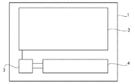
- FIG. 1 is a diagram showing functional blocks of a semiconductor integrated circuit (hereinafter referred to as “the present integrated circuit”) 1 according to the present embodiment.
- the integrated circuit 1 includes a circuit under measurement 2 including a plurality of connected flip-flop circuits, a clock generation circuit 3, and a delay measurement circuit 4.
- the circuit under test 2 is a circuit whose delay is to be measured, and includes a plurality of flip-flop circuits FF, although not limited thereto.
- the flip-flop can store an input signal and is not limited as long as it has this function.
- the flip-flop has a combination of a master latch and a slave latch. Can be illustrated.
- the flip-flops are connected to the clock generation circuit 3, respectively, and can store a signal input according to the input of the clock signal and output a recorded value outside the flip-flop.
- the clock generation circuit 3 creates and outputs a clock signal as is apparent from the description of this specification.
- the frequency of the clock signal is variable, the clock generation circuit itself is calibrated, and operates accurately without delay.
- the delay measurement circuit 4 can measure the delay in the circuit under test.
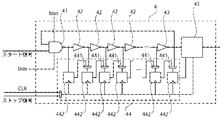
- the delay measurement circuit 4 according to the present embodiment is connected to a NAND circuit 41, a plurality of NOT circuits 42 connected in series to the NAND circuit 41, and terminals of the plurality of NOT circuits 42.
- the counter circuit 43 includes a scan chain circuit 44 to which a plurality of selector circuits 441 and a plurality of flip-flop circuits 442 are connected in a daisy chain.
- the NAND circuit 41 is a logic output circuit, and outputs a clock signal as a start signal generated by the clock generation circuit 3 and the terminal of a plurality of NOT circuits (delay circuits) connected to the NAND circuit 41. And at least two bias voltage input gates.
- this circuit is not limited, for example, the configuration shown in FIG. 3 can be shown.
- a plurality of switching elements are connected so that the source / drain regions of the switching elements adjacent to the NAND circuit 41 are conductive, and one end of the connection is grounded (GND). And the other end is connected to VDD.
- the NAND circuit 41 of this embodiment includes a bias voltage flow input gate in switching elements near both ends thereof. Specifically, one includes an n-type transistor and the other includes a p-type transistor. Connected to the bias power supply. As a result, the delay measuring circuit 4 has a variable delay time in the NAND circuit.
- a NAND circuit is used as the logic output circuit.
- a NOR circuit can be used as long as it can have the same function.
- the plurality of NOT circuits 42 of the present embodiment are delay circuits and are connected in series to the output of the NAND circuit as the logic output circuit, and the output of one NOT circuit is the input of the next NOT circuit.
- the value is also input to the selector circuit and the plurality of flip-flop circuits in the scan chain circuit.
- the number of NOT circuits is not particularly limited, and can be adjusted as appropriate according to the required delay measurement range, accuracy, and the like.
- the counter circuit 43 is connected to the ends of the plurality of NOT circuits, and counts the outputs of the end NOT circuits.
- the scan chain circuit 44 is connected to a plurality of selector circuits 441 and a plurality of flip-flop circuits 442, and is connected to the output of each of the plurality of NOT circuits, and stores the values of those outputs. be able to.
- An example of the configuration of this circuit is as shown in FIG. Note that the scan chain circuit 44 is configured to accept an input of a clock signal as a stop signal generated by the clock generation circuit 3. When this stop signal is input, the scan chain circuit 44 holds a value at that time.
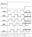
- FIG. 4 is a diagram illustrating a voltage signal in the delay measurement circuit calibration method according to the present embodiment.
- the clock generation circuit 3 generates and outputs a clock signal as a start signal.
- the clock generation circuit 3 generates and outputs a clock signal as a stop signal after a lapse of a certain period after generating the start signal.
- the measurement time T is between the start signal and the stop signal.
- the start signal changes, it is input to the NAND circuit, and a line (delay line (delay circuit)) configured by connecting a plurality of NOT circuits starts oscillating in response to the result.
- a line delay line (delay circuit)
- the counter value in the count circuit is incremented by 1 and at the same time the change in the value is again transmitted to the NAND circuit. Is propagated. In this figure, the odd-numbered values are inverted for easy understanding.
- the stop signal changes, the signal value on the delay line is stored in the scan chain, and at the same time, the counter circuit stops operating (the bold line in the figure is the value stored in the scan chain).
- the value of the counter is 5, and after the counter reaches 5, NAND, INV1 (the output of the first-stage NOT circuit, hereinafter the same in “INV”), INV2 changes, INV3, It can be observed that INVn has not changed. Therefore, in the case of this figure, it can be said that the time from the input of the start signal to the input of the stop signal is the sum of the following values. (1) Five times the delay time of the delay line (2) Sum of delay times of NAND circuits, INV1, INV2
- the increase d of the delay time in the NAND is determined for each p-type switching element and n-type switching element.
- a time T during which no change in NAND and INV is observed after a change in the counter value in the bias voltage is found.
- the time T at this time is T2, and the counter value is n2.
- d can be expressed by the equation T2 / n2-T1 / n1. Even in this case, it is preferable to set n2 as large as possible in order to increase the accuracy.
- FIG. 1 An example of the delay time of the NAND circuit in the change of the bias voltage of the p-type switching element and the change of the bias voltage of the n-type switching element is shown in FIG.
- the horizontal axis indicates the bias voltage
- the vertical axis indicates the delay time of the NAND circuit
- the circle indicates the upper limit of the delay time due to expected variations
- the triangle indicates the ideal delay time
- the square indicates the expected time.
- the lower limit of the delay time due to variation is shown.
- the delay time of the NAND gate when no bias voltage is applied is obtained by (d2-d1) n-d1.
- the measurement is the same as in (C) above. Specifically, when measuring the delay time of INVi, the minimum and maximum bias values V1 and V2 that are 1... 100... 0 (i is 1 consecutive) or 0... 011.
- the delay time of the NAND gate at this time is d1, d2, the counter value is n, and the delay time of INVi can be obtained from these values by (d2-d1) n.
- the calibration can be completed by performing the above (A) to (D).
- the present integrated circuit it is possible to provide a semiconductor integrated circuit, a delay measurement circuit, and a delay measurement circuit calibration method capable of highly accurate calibration without increasing the size of the circuit.
- the present invention has industrial applicability as a semiconductor integrated circuit.
Landscapes
- Engineering & Computer Science (AREA)
- General Engineering & Computer Science (AREA)
- Physics & Mathematics (AREA)
- General Physics & Mathematics (AREA)
- Semiconductor Integrated Circuits (AREA)
- Tests Of Electronic Circuits (AREA)
- Manipulation Of Pulses (AREA)
Abstract
本発明の一観点に係る半導体集積回路は、接続された複数のフリップフロップ回路を有する被測定回路部と、クロック生成回路部と、NAND回路と、NAND回路に直列に接続される複数のNOT回路と、複数のNOT回路の末端に接続されるカウンタ回路と、複数のセレクタ回路及び複数のフリップフロップ回路が接続されるスキャンチェーン回路と、を備えた遅延測定回路部と、を備えた半導体集積回路であって、NAND回路は、少なくとも二つのバイアス電圧入力ゲートを備えている。
Description
本発明は、半導体集積回路及び遅延測定回路に関し、更には遅延測定回路較正方法に関する。
半導体集積回路は、半導体材料若しくは絶縁材料の表面又は半導体材料の内部にトランジスタその他の回路素子を生成させ、電子回路の機能を有するよう設計したものであり、パーソナルコンピュータや携帯電話等に用いられており、特に近年、半導体集積回路における微細化技術の進歩によりめざましく高速化が図られている。
しかしながら、半導体集積回路の高速化は、トランジスタと配線の加工のばらつきや配線間の容量結合等の増加等に起因する回路における信号の伝播時間のばらつきをもたらし、このばらつきを如何に抑えるかが重要な課題となっている。すなわち高速動作が可能な半導体集積回路を歩留まりよく作製するためには回路における伝播時間及びその統計的なばらつきを把握し、改善していくことが必要である。この伝播時間が必要以上に長くなっていないかを確認する方法として遅延測定がある。
遅延測定とは、テスト信号を入力して応答信号を得るまでの時間を計測することをいい、この結果、計測した時間が所定の期間内に納まっているか否かを判定し、不良品であるか否かを判断することができる。
ところが、半導体集積回路に搭載される遅延測定を行う回路自体も製造バラつきの影響を受け、その測定自体に誤差が生じることとなる。その場合、正確な遅延測定を行うことは困難となってしまう。
そこで、公知の技術として、例えば下記特許文献1及び2に、遅延測定回路におけるバラつきによる測定誤差を軽減する技術が開示されている。
しかしながら、上記特許文献1に記載の技術では、電圧降下や温度変化等、グローバルなばらつきによる測定誤差に対応することができるが、各遅延素子の製造ばらつきなどのローカルなばらつきには対応することができない。また、高精度な較正が困難である。また、上記特許文献2に記載の技術では複数のディレイラインを用いており、大型化してしまうといった課題が残る。
そこで、本発明は、上記課題に鑑み、回路の大型化をもたらさずに高精度な較正が可能な半導体集積回路及び遅延測定回路を提供することを目的とする。
上記課題を解決する本発明の一観点に係る遅延測定回路は、クロック生成回路と、論理出力回路と、前記論理出力回路に直列に接続される複数の遅延回路と、複数の遅延回路の末端に接続されるカウンタ回路と、を有する遅延測定回路と、を備えた遅延測定回路であって、論理出力回路及び複数の遅延回路の少なくとも一つは遅延時間が可変である。
また、本観点において、論理出力回路は、NAND回路及びNOR回路の少なくともいずれかを含むことが好ましい。
また、本観点において、遅延回路は、NOT回路及びバッファ回路の少なくともいずれかを含むことが好ましい。
また、本観点において、複数のセレクタ回路及び複数のフリップフロップ回路が接続されたスキャンチェーン回路を備えることが好ましい。
また、本発明の他の一観点に係る半導体集積回路は、被測定回路と、クロック生成回路と、論理出力回路と、論理出力回路に直列に接続される複数の遅延回路と、複数の遅延回路の末端に接続されるカウンタ回路と、を有する遅延測定回路と、を備えた半導体集積回路であって、論理出力回路及び前記複数の遅延回路の少なくとも一つは、少なくとも二つのバイアス電圧入力ゲートを備える。
また、本観点において、論理出力回路は、NAND回路及びNOR回路の少なくともいずれかを含むことが好ましい。
また本観点において、遅延回路は、NOT回路及びバッファ回路の少なくともいずれかを含む。
また本観点において、複数のセレクタ回路及び複数のフリップフロップ回路が接続されたスキャンチェーン回路を備えることが好ましい。
また本発明の他の一観点に係る半導体集積回路は、接続された複数のフリップフロップ回路を有する被測定回路部と、クロック生成回路部と、NAND回路と、NAND回路に直列に接続される複数のNOT回路と、複数のNOT回路の末端に接続されるカウンタ回路と、複数のセレクタ回路及び複数のフリップフロップ回路が接続されるスキャンチェーン回路と、を備えた遅延測定回路部と、を備えた半導体集積回路であって、NAND回路は、少なくとも二つのバイアス電圧入力ゲートを備えている。
また本発明の他の一観点に係る遅延測定回路は、NAND回路と、NAND回路に直列に接続される複数のNOT回路と、複数のNOT回路の末端に接続されるカウンタ回路と、複数のセレクタ回路及び複数のフリップフロップ回路が接続されるスキャンチェーン回路と、を備えており、NAND回路は、少なくとも二つのバイアス電圧入力ゲートを備えている。
本発明は、上記課題に鑑み、回路の大型化をもたらさずに高精度な較正が可能な半導体集積回路及び遅延測定回路並びに遅延測定回路較正方法を提供することができる。
以下、本発明の実施形態について、図面を用いて詳細に説明する。ただし、本発明は多くの異なる形態による実施が可能であり、以下に示す実施形態、実施例の例示に限定されるものではない。
図1は、本実施形態に係る半導体集積回路(以下「本集積回路」という。)1の機能ブロックを示す図である。本図で示すように、本集積回路1は、接続された複数のフリップフロップ回路を備える被測定回路2と、クロック生成回路3と、遅延測定回路4と、を備えている。
本実施形態において被測定回路2は、遅延の測定対象となる回路であって、限定されるわけではないが、複数のフリップフロップ回路FFを有している。本実施形態においてフリップフロップは、入力される信号を記憶することのできるものであって、この機能を有する限りにおいて限定されるわけではないが、例えばマスターラッチとスレイブラッチとの組み合わせを備えたものを例示することができる。なお、フリップフロップは、クロック生成回路3にそれぞれ接続されており、クロック信号の入力に応じて入力された信号の記憶、フリップフロップ外への記録した値の出力を行うことができる。
本実施形態において、クロック生成回路3は、本明細書の記載から明らかなようにクロック信号を作成し、出力するものである。なお本実施形態において、クロック信号の周波数は可変であり、クロック生成回路自体は較正されており、遅延なく正確に動作する。
また本実施形態において、遅延測定回路4は、被測定回路における遅延を測定することができるものである。本実施形態に係る遅延測定回路4は、図2で示すように、NAND回路41と、NAND回路41に直列に接続される複数のNOT回路42と、複数のNOT回路42の末端に接続されるカウンタ回路43と、複数のセレクタ回路441及び複数のフリップフロップ回路442が数珠繋ぎで接続されるスキャンチェーン回路44、を備えている。
本実施形態においてNAND回路41は、論理出力回路であって、クロック生成回路3が生成するスタート信号としてのクロック信号と、NAND回路41に接続される複数のNOT回路(遅延回路)の末端の出力を入力信号とするとともに、少なくとも二つのバイアス電圧入力ゲートを備えている。この回路の具体的な構成については限定されるわけではないが、例えば図3で示す構成を示すことができる。本図で示すように、NAND回路41は、複数のスイッチング素子が、自己に隣接するスイッチング素子のソース/ドレイン領域が導通するよう接続されており、その接続の一方の端が接地(GND)されており、他方の端がVDDに接続されている。
また、本実施形態のNAND回路41では、その両端近傍のスイッチング素子において、バイアス電圧流入力ゲートを備えており、具体的には一方はn型のトランジスタ、他方はp型のトランジスタを備えており、バイアス電源に接続されている。この結果、本遅延測定回路4は、NAND回路が遅延時間可変となっている。なお、本実施形態の例では、論理出力回路としてNAND回路を用いているが、同様の機能を有することができるものであればNOR回路で構成することも可能である。
また本実施形態の複数のNOT回路42は、遅延回路であり、上記論理出力回路としてのNAND回路の出力に直列的に接続されており、一つのNOT回路の出力が次段のNOT回路の入力となっているとともに、スキャンチェーン回路におけるセレクタ回路及び複数のフリップフロップ回路にもその値が入力されるよう接続されている。なおNOT回路の数は特に限定されるものではなく、必要とされる遅延測定範囲、精度等に応じて適宜調整可能である。また、NOT回路のほか遅延回路としての機能を有する限り限定されず、遅延を生じさせるいわゆるバッファ回路を設けることも可能である。
また本実施形態において、カウンタ回路43は、上記のとおり、複数のNOT回路の末端に接続されており、末端のNOT回路の出力をカウントする。
また本実施形態においてスキャンチェーン回路44は、複数のセレクタ回路441及び複数のフリップフロップ回路442が接続されており、複数のNOT回路それぞれの出力に接続されており、それらの出力の値を記憶することができる。この回路の構成の一例については上記図2に示したとおりである。なお、スキャンチェーン回路44は、クロック生成回路3が生成するストップ信号としてのクロック信号の入力を受け付ける構成となっており、このストップ信号が入力された場合、その時における値を保持する。
(遅延測定の波形図)
次に、本集積回路を用いて、遅延時間測定を較正する方法について具体的に説明する。図4は、本実施形態における遅延測定回路較正方法における電圧信号を示す図である。
次に、本集積回路を用いて、遅延時間測定を較正する方法について具体的に説明する。図4は、本実施形態における遅延測定回路較正方法における電圧信号を示す図である。
まず、クロック生成回路3は、スタート信号としてのクロック信号を生成し、出力する。なお、クロック生成回路3は、スタート信号を生成した後、一定の期間経過後、ストップ信号としてのクロック信号を生成し、出力する。このスタート信号とストップ信号の間が測定時間Tとなる。
まず、スタート信号が変化すると、NAND回路に入力され、その結果を受けて複数のNOT回路の接続により構成されるライン(ディレイライン(遅延回路))が発振を始める。具体的には、NAND回路から順次値の変化が伝搬され、最後のNOT回路迄の値の変化が伝搬されるとカウント回路におけるカウンタ値が1加算されると同時に再びNAND回路にこの値の変化が伝搬される。なお本図ではわかりやすくするため、奇数番目の値を反転させている。
一方、ストップ信号が変化した時、ディレイライン上の信号値がスキャンチェーンへと記憶されると同時にカウンタ回路が動作を停止する(図中の太線がスキャンチェーンへ記憶される値)。なお本図の例では、カウンタの値は5であり、カウンタが5となった後NAND、INV1(1段目のNOT回路の出力、以下「INV」において同じ)、INV2が変化し、INV3、からINVnが変化していないことが観測できる。よって、本図の場合、スタート信号が入力されてからストップ信号が入力されるまでの時間は、以下の値の和であるといえる。
(1)ディレイラインの遅延時間の5倍
(2)NAND回路、INV1、INV2の遅延時間の和
(1)ディレイラインの遅延時間の5倍
(2)NAND回路、INV1、INV2の遅延時間の和
(NANDゲートの特性)
立ち上がり、立下り遅延時間を調整するためにはn型スイッチング素子、p型スイッチング側のバイアス電圧を変化させることで可能である。ディレイラインはチップ内に埋め込まれており、製造によるばらつきの影響を受けてしまう。したがって、バイアス電圧と遅延時間の関係を設計時に知ることは出来ない。そこで、下記手順による測定を行うことで較正を行う。ここではクロック信号生成回路によるクロック信号は正確であり、このクロック信号であるスタート信号及びストップ信号の間の時間を既知とし、調整することで各測定を行う。
立ち上がり、立下り遅延時間を調整するためにはn型スイッチング素子、p型スイッチング側のバイアス電圧を変化させることで可能である。ディレイラインはチップ内に埋め込まれており、製造によるばらつきの影響を受けてしまう。したがって、バイアス電圧と遅延時間の関係を設計時に知ることは出来ない。そこで、下記手順による測定を行うことで較正を行う。ここではクロック信号生成回路によるクロック信号は正確であり、このクロック信号であるスタート信号及びストップ信号の間の時間を既知とし、調整することで各測定を行う。
(A)ディレイライン全体の遅延時間測定
まずカウンタの値が変化してからNAND、INVの値が観測されない(スキャンフリップフロップの値が全て0又は全て1である)時間Tを探す。このときのTをT1とし、カウンタの値をn1とする。ここでn1はなるべく大きな値にすることが好ましい。そしてこの結果、T1/n1がディレイライン全体の遅延時間であるとして求めることができる。なお、通常T1の分解能はあまり高くないが、n1を大きくすることによって結果に対する分解能を高めることができる。
まずカウンタの値が変化してからNAND、INVの値が観測されない(スキャンフリップフロップの値が全て0又は全て1である)時間Tを探す。このときのTをT1とし、カウンタの値をn1とする。ここでn1はなるべく大きな値にすることが好ましい。そしてこの結果、T1/n1がディレイライン全体の遅延時間であるとして求めることができる。なお、通常T1の分解能はあまり高くないが、n1を大きくすることによって結果に対する分解能を高めることができる。
(B)NANDゲートのバイアス電圧と遅延時間の関係を求める
p型のスイッチング素子、n型のスイッチング素子毎にNANDにおける遅延時間の増加dを求める。バイアス電圧においてカウンタの値が変化してからNAND、INVの変化が観測されない時間Tを探し、この時の時間TをT2とし、カウンタの値をn2とする。ここで、dはT2/n2-T1/n1という式で表せる。なおこの場合においても精度を高めるためにn2はなるべく大きな値にしておくことが好ましい。なお、p型のスイッチング素子のバイアス電圧の変化、n型のスイッチング素子のバイアス電圧の変化におけるNAND回路の遅延時間一例について図5に示しておく。なお図中、横軸はバイアス電圧を、縦軸はNAND回路の遅延時間を、丸印は予想されるばらつきによる遅延時間の上限を、三角印は遅延時間の理想値を、四角印は予想されるばらつきによる遅延時間の下限をそれぞれ示している。
p型のスイッチング素子、n型のスイッチング素子毎にNANDにおける遅延時間の増加dを求める。バイアス電圧においてカウンタの値が変化してからNAND、INVの変化が観測されない時間Tを探し、この時の時間TをT2とし、カウンタの値をn2とする。ここで、dはT2/n2-T1/n1という式で表せる。なおこの場合においても精度を高めるためにn2はなるべく大きな値にしておくことが好ましい。なお、p型のスイッチング素子のバイアス電圧の変化、n型のスイッチング素子のバイアス電圧の変化におけるNAND回路の遅延時間一例について図5に示しておく。なお図中、横軸はバイアス電圧を、縦軸はNAND回路の遅延時間を、丸印は予想されるばらつきによる遅延時間の上限を、三角印は遅延時間の理想値を、四角印は予想されるばらつきによる遅延時間の下限をそれぞれ示している。
(C)バイアス電圧を加えない場合におけるNDNDゲートの遅延時間測定
そして、スキャンフリップフロップの値が1000…0又は0111…1である時間Tを探す。バイアス電圧をかけるとフリップフロップの値は0000…0又は1111…1を経て0000…1又は1111…0へと変化するため、0000…0又は1111…1となる最小又は最大のバイアス値を求めV1、V2とする。なおこの場合においてV1、V2に対応する遅延時間の増加量をd1、d2(d2>d1)とする。なおこの場合において、カウンタの値は常にnであるとする。
そして、スキャンフリップフロップの値が1000…0又は0111…1である時間Tを探す。バイアス電圧をかけるとフリップフロップの値は0000…0又は1111…1を経て0000…1又は1111…0へと変化するため、0000…0又は1111…1となる最小又は最大のバイアス値を求めV1、V2とする。なおこの場合においてV1、V2に対応する遅延時間の増加量をd1、d2(d2>d1)とする。なおこの場合において、カウンタの値は常にnであるとする。
すると、バイアス電圧を加えないときのNANDゲートの遅延時間は(d2-d1)n-d1によって得られる。なおこの場合において、nは、d1、d2の誤差の影響をなるべく小さくするため、小さくすることが好ましい。より具体的には、n1、n2と同程度に大きなnを用いてしまうとクロック信号生成回路の分解能と同程度にまで測定精度が落ちてしまうので注意が必要である。
(D)各NOT回路の遅延時間を測定する
上記(C)と同様の測定によって行う。具体的には、INViの遅延時間を測定する場合は、1…100…0(1がi個連続)又は0…011…1(0がi個連続)である最小最大のバイアス値V1、V2を求め、この時のNANDゲートの遅延時間をd1、d2、カウンタ値をnとし、これらの値からINViの遅延時間は(d2-d1)nによって求めることができる。
上記(C)と同様の測定によって行う。具体的には、INViの遅延時間を測定する場合は、1…100…0(1がi個連続)又は0…011…1(0がi個連続)である最小最大のバイアス値V1、V2を求め、この時のNANDゲートの遅延時間をd1、d2、カウンタ値をnとし、これらの値からINViの遅延時間は(d2-d1)nによって求めることができる。
すなわち、上記(A)~(D)を実施することにより、較正を完了させることができる。
以上本集積回路によると、回路の大型化をもたらさずに高精度な較正が可能な半導体集積回路及び遅延測定回路並びに遅延測定回路較正方法を提供することができる。
本発明は、半導体集積回路として産業上利用可能性がある。
Claims (10)
- クロック生成回路と、
論理出力回路と、前記論理出力回路に直列に接続される複数の遅延回路と、前記複数の遅延回路の末端に接続されるカウンタ回路と、を有する遅延測定回路と、を備えた遅延測定回路であって、
前記論理出力回路及び前記複数の遅延回路の少なくとも一つは、遅延時間可変である遅延測定回路。 - 前記論理出力回路は、NAND回路及びNOR回路の少なくともいずれかを含む請求項1記載の遅延測定回路。
- 前記遅延回路は、NOT回路及びバッファ回路の少なくともいずれかを含む請求項1記載の遅延測定回路。
- 複数のセレクタ回路及び複数のフリップフロップ回路が接続されたスキャンチェーン回路を備える請求項1記載の遅延測定回路。
- 被測定回路と、
クロック生成回路と、
論理出力回路と、前記論理出力回路に直列に接続される複数の遅延回路と、前記複数の遅延回路の末端に接続されるカウンタ回路と、を有する遅延測定回路と、を備えた半導体集積回路であって、
前記論理出力回路及び前記複数の遅延回路の少なくとも一つは、少なくとも二つのバイアス電圧入力ゲートを備える半導体集積回路。 - 前記論理出力回路は、NAND回路及びNOR回路の少なくともいずれかを含む請求項5記載の半導体集積回路。
- 前記遅延回路は、NOT回路及びバッファ回路の少なくともいずれかを含む請求項5記載の半導体集積回路。
- 複数のセレクタ回路及び複数のフリップフロップ回路が接続されたスキャンチェーン回路を備える請求項5記載の半導体集積回路。
- 接続された複数のフリップフロップ回路を有する被測定回路と、
クロック生成回路と、
NAND回路と、前記NAND回路に直列に接続される複数のNOT回路と、複数の前記NOT回路の末端に接続されるカウンタ回路と、複数のセレクタ回路及び複数のフリップフロップ回路が接続されるスキャンチェーン回路と、を有する遅延測定回路と、を備えた半導体集積回路であって、
前記NAND回路は、少なくとも二つのバイアス電圧入力ゲートを備える半導体集積回路。 - NAND回路と、前記NAND回路に直列に接続される複数のNOT回路と、複数の前記NOT回路の末端に接続されるカウンタ回路と、複数のセレクタ回路及び複数のフリップフロップ回路が接続されるスキャンチェーン回路と、を備え、
前記NAND回路は、少なくとも二つのバイアス電圧入力ゲートを備えた遅延測定回路。
Priority Applications (1)
| Application Number | Priority Date | Filing Date | Title |
|---|---|---|---|
| JP2016543089A JP6218297B2 (ja) | 2015-03-05 | 2016-03-04 | 半導体集積回路及び遅延測定回路 |
Applications Claiming Priority (2)
| Application Number | Priority Date | Filing Date | Title |
|---|---|---|---|
| JP2015044113 | 2015-03-05 | ||
| JP2015-044113 | 2015-03-05 |
Publications (1)
| Publication Number | Publication Date |
|---|---|
| WO2016139958A1 true WO2016139958A1 (ja) | 2016-09-09 |
Family
ID=56849298
Family Applications (1)
| Application Number | Title | Priority Date | Filing Date |
|---|---|---|---|
| PCT/JP2016/001185 Ceased WO2016139958A1 (ja) | 2015-03-05 | 2016-03-04 | 半導体集積回路及び遅延測定回路 |
Country Status (2)
| Country | Link |
|---|---|
| JP (1) | JP6218297B2 (ja) |
| WO (1) | WO2016139958A1 (ja) |
Cited By (1)
| Publication number | Priority date | Publication date | Assignee | Title |
|---|---|---|---|---|
| WO2024224868A1 (ja) * | 2023-04-24 | 2024-10-31 | 富士通株式会社 | 配線ばらつき算出方法および配線ばらつき算出プログラム |
Citations (3)
| Publication number | Priority date | Publication date | Assignee | Title |
|---|---|---|---|---|
| JP2007322235A (ja) * | 2006-05-31 | 2007-12-13 | Denso Corp | 時間計測回路 |
| JP2011113984A (ja) * | 2009-11-23 | 2011-06-09 | Chiba Univ | 半導体集積回路及びその遅延測定方法 |
| JP2012114716A (ja) * | 2010-11-25 | 2012-06-14 | Renesas Electronics Corp | Tdc装置とtdcのキャリブレーション方法 |
Family Cites Families (4)
| Publication number | Priority date | Publication date | Assignee | Title |
|---|---|---|---|---|
| JP3064644B2 (ja) * | 1992-03-16 | 2000-07-12 | 株式会社デンソー | A/d変換回路 |
| JP2002076856A (ja) * | 2000-08-30 | 2002-03-15 | Sony Corp | バイアス信号生成回路、遅延回路、発振回路およびクロック群発生回路 |
| JP3991969B2 (ja) * | 2003-09-17 | 2007-10-17 | 株式会社デンソー | A/d変換回路 |
| JP5303830B2 (ja) * | 2006-03-16 | 2013-10-02 | 富士通株式会社 | ピリオドジッタキャンセル回路、静的位相差キャンセル回路、ピリオドジッタ測定回路、静的位相差測定回路及び位相差調整回路 |
-
2016
- 2016-03-04 JP JP2016543089A patent/JP6218297B2/ja not_active Expired - Fee Related
- 2016-03-04 WO PCT/JP2016/001185 patent/WO2016139958A1/ja not_active Ceased
Patent Citations (3)
| Publication number | Priority date | Publication date | Assignee | Title |
|---|---|---|---|---|
| JP2007322235A (ja) * | 2006-05-31 | 2007-12-13 | Denso Corp | 時間計測回路 |
| JP2011113984A (ja) * | 2009-11-23 | 2011-06-09 | Chiba Univ | 半導体集積回路及びその遅延測定方法 |
| JP2012114716A (ja) * | 2010-11-25 | 2012-06-14 | Renesas Electronics Corp | Tdc装置とtdcのキャリブレーション方法 |
Cited By (1)
| Publication number | Priority date | Publication date | Assignee | Title |
|---|---|---|---|---|
| WO2024224868A1 (ja) * | 2023-04-24 | 2024-10-31 | 富士通株式会社 | 配線ばらつき算出方法および配線ばらつき算出プログラム |
Also Published As
| Publication number | Publication date |
|---|---|
| JPWO2016139958A1 (ja) | 2017-04-27 |
| JP6218297B2 (ja) | 2017-10-25 |
Similar Documents
| Publication | Publication Date | Title |
|---|---|---|
| CN105445569B (zh) | 一种适用于高速集成电路的片上纳秒级电源噪声瞬态波形测量系统及其测量方法 | |
| CN104101827B (zh) | 一种基于自定时振荡环的工艺角检测电路 | |
| CN102655410B (zh) | 压控振荡器、用于检测工艺波动的测试系统及其测试方法 | |
| CN103650345A (zh) | 部件分析系统及方法 | |
| JP5752577B2 (ja) | 半導体集積回路 | |
| KR100849208B1 (ko) | 링 오실레이터를 구비하는 테스트 회로 및 테스트 방법 | |
| US12210059B2 (en) | Test element group and test method | |
| US20090144677A1 (en) | Design Structure for a Circuit and Method to Measure Threshold Voltage Distributions in SRAM Devices | |
| CN103973303A (zh) | 环形振荡器和半导体装置 | |
| CN101706553B (zh) | 一种片上通路时延测量电路及方法 | |
| TWI521220B (zh) | 積體電路的時序分析方法及相關的電腦程式產品 | |
| CN103941178B (zh) | 一种检测集成电路制造工艺中工艺波动的检测电路 | |
| KR102166653B1 (ko) | 재구성 가능한 지연 회로, 및 그 지연 회로를 사용한 지연 모니터 회로, 편차 보정 회로, 편차 측정 방법 및 편차 보정 방법 | |
| JP2010109115A (ja) | オンチップ型のモニタ回路および半導体装置 | |
| JP6218297B2 (ja) | 半導体集積回路及び遅延測定回路 | |
| JP6610216B2 (ja) | 遅延回路および遅延回路の試験方法 | |
| US10054632B2 (en) | Semiconductor apparatus and characteristic measurement circuit therefor | |
| JP2015215213A (ja) | 半導体装置および半導体装置の制御方法 | |
| JP2012156203A (ja) | 半導体物性ばらつきセンサ及び集積回路 | |
| US20240201254A1 (en) | Jitter measuring circuit, jitter analyzing apparatus including the same, and related methods of manufacturing semiconductor devices | |
| JPH0720204A (ja) | 半導体チップ上の論理回路の遅延時間測定回路 | |
| JP5978797B2 (ja) | 基板電位検出回路、半導体集積回路及び基板電位検出回路の較正方法 | |
| CN120948995A (zh) | 器件自热效应延迟的测试结构和方法 | |
| US20090189660A1 (en) | Semiconductor device | |
| Al-Frajat et al. | Area efficient test circuit for library standard cell qualification |
Legal Events
| Date | Code | Title | Description |
|---|---|---|---|
| ENP | Entry into the national phase |
Ref document number: 2016543089 Country of ref document: JP Kind code of ref document: A |
|
| 121 | Ep: the epo has been informed by wipo that ep was designated in this application |
Ref document number: 16758654 Country of ref document: EP Kind code of ref document: A1 |
|
| NENP | Non-entry into the national phase |
Ref country code: DE |
|
| 122 | Ep: pct application non-entry in european phase |
Ref document number: 16758654 Country of ref document: EP Kind code of ref document: A1 |