WO2016136817A1 - 含フッ素組成物、パターン形成用基板、光分解性カップリング剤、パターン形成方法及びトランジスタの製造方法 - Google Patents
含フッ素組成物、パターン形成用基板、光分解性カップリング剤、パターン形成方法及びトランジスタの製造方法 Download PDFInfo
- Publication number
- WO2016136817A1 WO2016136817A1 PCT/JP2016/055456 JP2016055456W WO2016136817A1 WO 2016136817 A1 WO2016136817 A1 WO 2016136817A1 JP 2016055456 W JP2016055456 W JP 2016055456W WO 2016136817 A1 WO2016136817 A1 WO 2016136817A1
- Authority
- WO
- WIPO (PCT)
- Prior art keywords
- substrate
- fluorine
- containing composition
- pattern
- pattern forming
- Prior art date
Links
Images


Classifications
-
- B—PERFORMING OPERATIONS; TRANSPORTING
- B05—SPRAYING OR ATOMISING IN GENERAL; APPLYING FLUENT MATERIALS TO SURFACES, IN GENERAL
- B05D—PROCESSES FOR APPLYING FLUENT MATERIALS TO SURFACES, IN GENERAL
- B05D1/00—Processes for applying liquids or other fluent materials
- B05D1/32—Processes for applying liquids or other fluent materials using means for protecting parts of a surface not to be coated, e.g. using stencils, resists
-
- B—PERFORMING OPERATIONS; TRANSPORTING
- B05—SPRAYING OR ATOMISING IN GENERAL; APPLYING FLUENT MATERIALS TO SURFACES, IN GENERAL
- B05D—PROCESSES FOR APPLYING FLUENT MATERIALS TO SURFACES, IN GENERAL
- B05D3/00—Pretreatment of surfaces to which liquids or other fluent materials are to be applied; After-treatment of applied coatings, e.g. intermediate treating of an applied coating preparatory to subsequent applications of liquids or other fluent materials
- B05D3/10—Pretreatment of surfaces to which liquids or other fluent materials are to be applied; After-treatment of applied coatings, e.g. intermediate treating of an applied coating preparatory to subsequent applications of liquids or other fluent materials by other chemical means
-
- G—PHYSICS
- G03—PHOTOGRAPHY; CINEMATOGRAPHY; ANALOGOUS TECHNIQUES USING WAVES OTHER THAN OPTICAL WAVES; ELECTROGRAPHY; HOLOGRAPHY
- G03F—PHOTOMECHANICAL PRODUCTION OF TEXTURED OR PATTERNED SURFACES, e.g. FOR PRINTING, FOR PROCESSING OF SEMICONDUCTOR DEVICES; MATERIALS THEREFOR; ORIGINALS THEREFOR; APPARATUS SPECIALLY ADAPTED THEREFOR
- G03F7/00—Photomechanical, e.g. photolithographic, production of textured or patterned surfaces, e.g. printing surfaces; Materials therefor, e.g. comprising photoresists; Apparatus specially adapted therefor
- G03F7/004—Photosensitive materials
- G03F7/075—Silicon-containing compounds
Definitions
- the present invention relates to a fluorine-containing composition, a pattern forming substrate, a photodegradable coupling agent, a pattern forming method, and a transistor manufacturing method.
- This application claims priority based on Japanese Patent Application No. 2015-035424 filed in Japan on February 25, 2015 and Japanese Patent Application No. 2016-027241 filed in Japan on February 16, 2016. The contents are incorporated herein.
- a self-assembled monolayer With a self-assembled monolayer, by using an organic molecule having a functional group that forms a predetermined chemical bond as a terminal group for a predetermined substrate, a chemical bond is formed on the surface of the substrate, An anchored organic molecule is in a state of being ordered and formed into a monomolecular film by regulation from the substrate surface and interaction between organic molecules. Since this self-assembled monomolecular film has a simple manufacturing method, it can be easily formed on a substrate.
- the electrical characteristics of the organic transistors produced may be improved by controlling the wettability and lipophilicity of the substrate surface.
- an organic thin film such as a monomolecular film.
- a pattern forming method using the difference in surface characteristics on the substrate for example, there is a method in which a hydrophilic region and a water repellent region are formed on the substrate, and an aqueous solution of a functional material is applied to the hydrophilic region. In this method, since the aqueous solution of the functional material spreads only in the hydrophilic region, a thin film pattern of the functional material can be formed.
- Patent Document 1 by forming a self-assembled monolayer using a photodegradable silane coupling agent on a substrate and modifying the surface, the contact angle is greatly changed before and after light irradiation, It is disclosed that a hydrophilic region and a water-repellent region can be formed on a substrate.
- Organic thin films such as self-assembled monolayers are effective for modifying the surface of materials.
- the photodegradable silane coupling agent shown in Patent Document 1 can greatly change the contact angle before and after light irradiation and contribute to the modification of the substrate surface, in order to improve the characteristics of the organic thin film to be formed There was still room for improvement.
- the present invention has been made in view of the above circumstances, and can be suitably used for forming an organic thin film having good characteristics, and for pattern formation using the fluorine-containing composition. It is an object to provide a substrate, a photodegradable coupling agent, and a pattern forming method.
- the first aspect of the present invention is a fluorine-containing composition containing a fluorine-containing compound represented by the following general formula (1) and a fluorine-based solvent.
- X represents a halogen atom or an alkoxy group
- R 1 represents a hydrogen atom or a linear, branched or cyclic alkyl group having 1 to 10 carbon atoms
- R f1 and R f2 are each independently a fluorinated alkoxy group
- n represents an integer of 0 or more.
- the second aspect of the present invention is a pattern forming substrate having a surface chemically modified with the fluorine-containing composition of the first aspect.
- the third aspect of the present invention is a photodegradable coupling agent comprising the fluorine-containing composition of the first aspect.
- a fourth aspect of the present invention there is provided a method for forming a pattern on a surface to be processed of an object, wherein the surface to be processed is chemically modified using the fluorine-containing composition according to the first aspect.
- a method of forming a circuit pattern for an electronic device on a flexible substrate wherein the entire surface of the substrate or a specific region is formed on the first aspect.
- a first step of chemically modifying the fluorine-containing composition, and exposing the surface of the chemically modified substrate to generate a latent image of the circuit pattern on the surface of the substrate due to a difference in water repellency A fluid pattern forming material is brought into contact with a portion of the latent image on the surface of the substrate, and the pattern forming material is formed on the substrate in the shape of the circuit pattern due to the difference in water repellency.
- a third step of capturing the pattern is provided.
- a sixth aspect of the present invention is a method for forming a circuit pattern for an electronic device on a predetermined substrate, wherein the fluorine-containing composition according to the first aspect of the present invention is applied onto the substrate.
- a step of forming a fluorine-containing composition layer, exposing the fluorine-containing composition layer formed on the substrate with a predetermined pattern light, and a latent image of the circuit pattern due to a difference in water repellency on the substrate A pattern forming method including a step of forming an electroless plating, and a step of bringing an electroless plating catalyst into contact with the latent image portion to perform electroless plating.
- the pattern forming material preferably includes a liquid conductive material, a liquid semiconductor material, or a liquid insulating material.
- the light irradiated at the time of exposure includes light included in a wavelength region of 200 nm to 450 nm.
- a seventh aspect of the present invention is a method for manufacturing a transistor having a gate electrode, a source electrode, and a drain electrode, wherein at least one of the gate electrode, the source electrode, and the drain electrode is A transistor manufacturing method including the step of forming by the pattern forming method according to any one of the fourth to sixth aspects of the present invention.
- the schematic diagram which shows the whole structure of the suitable substrate processing apparatus in the pattern formation method of the aspect of this invention. It is a figure which shows an example of the schematic process drawing of the pattern formation method of the aspect of this invention. It is a figure which shows an example of the schematic process drawing of the manufacturing method of the transistor of the aspect of this invention.
- the first aspect of the present invention is a fluorine-containing composition containing the fluorine-containing compound represented by the general formula (1) and a fluorine-based solvent. Below, the fluorine-containing compound which the fluorine-containing composition of the aspect of this invention contains is demonstrated.
- the fluorine-containing compound is represented by the following general formula (1).
- X represents a halogen atom or an alkoxy group
- R 1 represents a hydrogen atom or a linear, branched or cyclic alkyl group having 1 to 10 carbon atoms
- R f1 and R f2 are each independently a fluorinated alkoxy group
- n represents an integer of 0 or more.
- X is a halogen atom or an alkoxy group.
- the halogen atom represented by X include a fluorine atom, a chlorine atom, a bromine atom, and an iodine atom.
- X is preferably an alkoxy group rather than a halogen atom.
- n represents an integer, and is preferably an integer of 1 to 20, and more preferably an integer of 2 to 15 from the viewpoint of easy availability of starting materials.
- R 1 is a hydrogen atom or a linear, branched or cyclic alkyl group having 1 to 10 carbon atoms.
- the alkyl group for R 1 is preferably a linear or branched alkyl group having 1 to 5 carbon atoms, and specifically includes a methyl group, an ethyl group, a propyl group, an isopropyl group, an n-butyl group, an isobutyl group. Group, tert-butyl group, pentyl group, isopentyl group, neopentyl group and the like.
- cyclic alkyl group examples include groups in which one or more hydrogen atoms have been removed from a polycycloalkane such as monocycloalkane, bicycloalkane, tricycloalkane, and tetracycloalkane.
- R 1 is preferably a hydrogen atom, a methyl group, an ethyl group or an isopropyl group, and more preferably a methyl group or an isopropyl group.
- R f1 and R f2 are each independently a fluorinated alkoxy group.
- the fluorinated alkoxy group represented by R f1 and R f2 is preferably an alkoxy group having 3 or more carbon atoms, and may be partially fluorinated. It may be a group. In the embodiment of the present invention, it is preferably a partially fluorinated alkoxy group.
- examples of the fluorinated alkoxy group for R f1 and R f2 include a group represented by —O— (CH 2 ) n f1 — (C n f2 F 2n f2 +1 ).
- N f1 is an integer of 0 or more
- n f2 is an integer of 0 or more.
- the fluorinated alkoxy groups for R f1 and R f2 may be the same or different, but are preferably the same from the viewpoint of ease of synthesis.
- the fluorinated alkoxy group for R f1 and R f2 is preferably a long fluoroalkyl chain.
- n f1 is preferably from 0 to 10, more preferably from 0 to 5, particularly preferably from 0 to 3, and most preferably 3.
- n f2 is preferably 1 to 15, more preferably 4 to 15, particularly preferably 6 to 12, and most preferably 7 to 10.
- n f2 is preferably an even number from the viewpoint of availability of materials and synthesis.
- the water repellency of the organic thin film formed using the fluorine-containing composition of the aspect of this invention can be maintained as n f2 is more than the said lower limit.
- the coating property of the pattern forming material such as metal ink is improved while maintaining the water repellency of the organic thin film formed using the fluorine-containing composition of the aspect of the present invention. be able to.
- n is an integer of 0 or more. In the embodiment of the present invention, n is preferably 3 or more. Further, n is preferably 10 or less, and more preferably 5 or less. The upper limit value and the lower limit value can be arbitrarily combined.
- the fluorine-containing compound can be obtained, for example, through the following first to fifth steps. As an example, a case where R f1 and R f2 are the same is shown.
- R 1, R f1 and R f2 are the same as R 1, R f1 and R f2 in the formula (1), R f1 'and R f2' is a fluorinated alkyl group.
- R 1, R f1 and R f2 are the same as R 1, R f1 and R f2 in the general formula (1).
- R 1, R f1 and R f2 are the same as R 1, R f1 and R f2 in the general formula (1).
- R 1, R f1, R f2 is as described for R 1, R f1, R f2 in the formula (1).
- the fluorine-containing composition of the embodiment of the present invention contains a fluorine-based solvent having a fluorine atom in the molecule.
- examples of the fluorine-based solvent include hexafluoro-m-xylene (HFX), hydrochlorofluorocarbon (HCFC), hydrofluorocarbon (HFC), perfluorocarbon (PFC), and ether-based hydrofluoroether (HFE).
- PFPE Perfluoropolyether
- HFPE hydrofluoroether
- 1,3-bistrifluoromethylbenzene 1,1,2,2,3,4,5,5,5-decafluoropentane
- 1,2,2,3,3,4-heptafluorocyclopentane 1,4-bistrifluoromethylbenzene.
- solvents may be used alone or in combination of two or more.
- hexafluoro-m-xylene (HFX) is preferable.
- the fluorinated composition of the embodiment of the present invention contains a fluorinated solvent, the fluorinated alkyl group in the fluorinated compound does not aggregate in the solvent and decomposes uniformly. A smooth film can be formed.
- the above-mentioned fluorine-containing compounds may be used alone or in combination of two or more.
- the compound concentration of the fluorine-containing compound is preferably 0.05 to 1.0 mM, more preferably 0.075 to 0.5 mM, more preferably 0.0. 085 to 0.2 mM is particularly preferred.
- the fluorine-containing composition according to the embodiment of the present invention includes stabilizers (ultraviolet absorbers, antioxidants, thermal polymerization inhibitors, etc.), surfactants (leveling agents) within the range that does not impair the effects of the present invention.
- stabilizers ultraviolet absorbers, antioxidants, thermal polymerization inhibitors, etc.
- surfactants leveling agents
- Antifoaming agents, suspending agents, dispersing agents, etc. may be added.
- the second aspect of the present invention is a pattern forming substrate having a surface chemically modified with the fluorinated composition.
- the surface of the pattern forming substrate according to an aspect of the present invention is modified with the fluorine-containing composition. For this reason, by selectively exposing through a mask or the like, a hydrophilic region is formed on the exposed portion and a water-repellent region is formed on the unexposed portion on the pattern forming substrate.
- the pattern forming material By applying the pattern forming material on the substrate on which the hydrophilic region and the water repellent region are formed, the pattern forming material can be selectively applied to the hydrophilic region formed in the exposed portion. Etc. can be formed.
- the shape of the substrate is not particularly limited, and a flat surface, a curved surface, or a partially curved surface is preferable, and a flat surface is more preferable. Further, the area of the substrate is not particularly limited, and a substrate having a surface having a size as long as a conventional coating method can be applied can be employed.
- the surface chemically modified with the fluorinated composition is preferably formed on one side of a flat substrate.
- pre-treat the substrate surface When modifying the surface of the substrate, it is preferable to pre-treat the substrate surface.
- pretreatment method pretreatment with a piranha solution or pretreatment with a UV-ozone cleaner is preferable.
- the method for modifying the surface of the substrate is not particularly limited as long as the X bonded to the reactive Si in the general formula (1) is bonded to the substrate, such as an immersion method or a chemical treatment method. A known method can be used.
- the third aspect of the present invention is a photodegradable coupling agent comprising the fluorine-containing composition.
- a photodegradable coupling agent according to an aspect of the present invention includes a photodegradable group having a liquid repellent group, and an attachment group X linked to the photodegradable group via a functional group. It has a fluorinated alkoxy chain R f1 or R f2 at the terminal, and the functional group has an amino group as a residue after photolysis. Therefore, the photodegradable coupling agent of the aspect of the present invention can ensure a large difference in contact angle before and after light irradiation.
- a fourth aspect of the present invention is a pattern forming method for forming a pattern on a surface to be processed of an object, wherein the surface to be processed is chemically modified using the fluorine-containing composition of the first aspect.
- a first step of exposing the chemically modified target to be processed to generate a latent image composed of a hydrophilic region and a water repellent region; and a step of disposing a pattern forming material in the hydrophilic region or the water repellent region. 3 is a pattern forming method.
- the first step is a step of chemically modifying the surface to be processed using the fluorine-containing composition of the first aspect in a pattern forming method for forming a pattern on the surface to be processed of an object.
- the object is not particularly limited.
- metals for example, metals, crystalline materials (eg, monocrystalline, polycrystalline and partially crystalline materials), amorphous materials, conductors, semiconductors, insulators, optical elements, painted substrates, fibers, glass , Ceramics, zeolites, plastics, thermosetting and thermoplastic materials (eg, optionally doped: polyacrylate, polycarbonate, polyurethane, polystyrene, cellulose polymer, polyolefin, polyamide, polyimide, resin, polyester, polyphenylene, etc.), film , Thin film, and foil.
- crystalline materials eg, monocrystalline, polycrystalline and partially crystalline materials
- amorphous materials e.g., conductors, semiconductors, insulators, optical elements, painted substrates, fibers, glass , Ceramics, zeolites, plastics, thermosetting and thermoplastic materials (eg, optionally doped: polyacrylate, polycarbonate, polyurethane, polystyrene,
- the pattern forming method of the aspect of the present invention it is preferable to form a circuit pattern for an electronic device on a flexible substrate.
- a foil such as a resin film or stainless steel
- the resin film is made of polyethylene resin, polypropylene resin, polyester resin, ethylene vinyl copolymer resin, polyvinyl chloride resin, cellulose resin, polyamide resin, polyimide resin, polycarbonate resin, polystyrene resin, vinyl acetate resin, etc. Can be used.
- the term “flexibility” refers to the property that the substrate can be bent without being broken or broken even if a force of its own weight is applied to the substrate.
- flexibility includes a property of bending by a force of about its own weight. The flexibility varies depending on the material, size, thickness, environment such as temperature, etc. of the substrate.
- the substrate may be a single band-shaped substrate, but may be configured to be formed in a band shape by connecting a plurality of unit substrates.
- the first step it is preferable to chemically modify the entire surface of the target surface of the object or a specific region using the fluorine-containing composition.
- the method for chemically modifying the surface to be treated of the object is not particularly limited as long as X in the general formula (1) bonded to the reactive Si is bonded to the substrate.
- a known method such as a processing method can be used.
- the chemical modification in the first step can be performed, for example, by reacting the fluorine-containing compound represented by the general formula (1) with a substrate having a hydroxyl group as shown below.
- X description of R 1, R f1, R f2 , n is the same as the description of the X, the R 1, R f1, R f2 , n in the general formula (1).
- the chemical modification in the first step may be performed by preparing a substrate having an amino group and reacting with an active carbonate containing a 2-nitrobenzyl group, as shown below.
- an active carbonate containing a 2-nitrobenzyl group as shown below.
- the second step is a step of exposing a chemically modified surface to be processed to generate a latent image composed of a hydrophilic region and a water repellent region.
- the light irradiated during exposure is preferably ultraviolet light.
- the light to be irradiated preferably includes light having a wavelength included in the range of 200 to 450 nm, and more preferably includes light having a wavelength included in the range of 320 to 450 nm. It is also preferable to irradiate light including light having a wavelength of 365 nm. Light having these wavelengths can efficiently decompose the photodegradable group of the embodiment of the present invention.
- Light sources include low-pressure mercury lamps, high-pressure mercury lamps, ultra-high-pressure mercury lamps, xenon lamps, sodium lamps; gas lasers such as nitrogen, liquid lasers of organic dye solutions, solid-state lasers containing rare earth ions in inorganic single crystals, etc. Can be mentioned.
- a light source other than the laser from which monochromatic light is obtained light having a specific wavelength obtained by extracting a broadband line spectrum or continuous spectrum using an optical filter such as a bandpass filter or a cutoff filter may be used. Since a large area can be irradiated at a time, a high pressure mercury lamp or an ultrahigh pressure mercury lamp is preferable as the light source.
- a high pressure mercury lamp or an ultrahigh pressure mercury lamp is preferable as the light source.
- light can be arbitrarily irradiated within the above range, but it is particularly preferable to irradiate light energy having a distribution corresponding to the circuit pattern.
- irradiation with light of a predetermined pattern on the chemically modified surface causes dissociation of a group having water repellency and a residue (amino group) having hydrophilic performance.
- a latent image consisting of a hydrophilic region and a water repellent region can be generated.
- the second step it is preferable to generate a latent image of the circuit pattern due to the difference in hydrophilicity / water repellency on the surface of the flexible substrate.
- ⁇ Two-stage surface conversion> In the step of irradiating a chemically modified surface with a predetermined pattern of light using the fluorine-containing composition of the embodiment of the present invention to generate a latent image composed of a hydrophilic region and a water-repellent region, two-step surface conversion A latent image including a hydrophilic region and a water-repellent region may be generated by a method.
- the two-stage surface conversion method first, as shown in [First stage] below, the substrate surface is surface-modified using the fluorine-containing composition of the embodiment of the present invention to make the substrate surface water-repellent.
- the surface of the substrate changed to hydrophilic in the first stage is repelled by applying activated carbonate or active ester to the substrate changed to hydrophilic in the first stage. It can be changed to an aqueous surface.
- R 1 , R f1 , R f2 , n are explained in the general formula (1) R 1 , R f1 , R f2 , This is the same as described for n.
- R f is a fluorinated alkyl group.
- the third step is a step of arranging the pattern forming material in the hydrophilic region or the water repellent region generated in the second step.
- a wiring material in which particles such as gold, silver, copper and alloys thereof are dispersed in a predetermined solvent, or a precursor solution containing the above-described metal, an insulator (resin), Examples thereof include an electronic material in which a semiconductor, an organic EL light emitting material and the like are dispersed in a predetermined solvent, a resist solution, and the like.
- the pattern forming material is preferably a liquid conductive material, a liquid semiconductor material, or a liquid insulating material.
- liquid conductive material examples include a pattern forming material made of a dispersion liquid in which conductive fine particles are dispersed in a dispersion medium.
- conductive fine particles for example, metal fine particles containing any one of gold, silver, copper, palladium, nickel and ITO, oxides thereof, and fine particles of conductive polymers and superconductors are used.
- These conductive fine particles can be used by coating the surface with an organic substance or the like in order to improve dispersibility.
- the dispersion medium is not particularly limited as long as it can disperse the conductive fine particles and does not cause aggregation.
- alcohols such as methanol, ethanol, propanol, butanol, n-heptane, n-octane, decane, dodecane, tetradecane, toluene, xylene, cymene, durene, indene, dipentene, tetrahydronaphthalene, decahydro Hydrocarbon compounds such as naphthalene and cyclohexylbenzene, ethylene glycol dimethyl ether, ethylene glycol diethyl ether, ethylene glycol methyl ethyl ether, diethylene glycol dimethyl ether, diethylene glycol diethyl ether, diethylene glycol methyl ethyl ether, 1,2-dimethoxyethane, bis (2- Methoxyethyl) ether, ether
- an organic semiconductor material dispersed or dissolved in a dispersion medium can be used.
- the organic semiconductor material a ⁇ -electron conjugated low molecular material or high molecular material whose skeleton is composed of conjugated double bonds is desirable.
- Typical examples include acenes such as pentacene, soluble low-molecular materials such as thienoacenes such as benzothienobenzothiophene, and soluble high-molecular materials such as polythiophene, poly (3-alkylthiophene), and polythiophene derivatives.
- Liquid insulating materials include polyimide, polyamide, polyester, acrylic, PSG (phosphorus glass), BPSG (phosphorus boron glass), polysilazane SOG, silicate SOG (Spin on Glass), alkoxysilicate SOG, and siloxane polymer.
- An insulating material in which SiO 2 or the like having a Si—CH 3 bond is dispersed or dissolved in a dispersion medium can be given.
- a droplet discharge method As a method for arranging the pattern forming material, a droplet discharge method, an ink jet method, a spin coat method, a roll coat method, a slot coat method, or the like can be applied.
- FIG. 1 shows the configuration of the substrate processing apparatus 100.
- the substrate processing apparatus 100 performs processing on a substrate supply unit 2 that supplies a strip-shaped substrate (for example, a strip-shaped film member) S and a surface (surface to be processed) Sa of the substrate S.
- Substrate processing unit 3 substrate collecting unit 4 for collecting substrate S, fluorine-containing composition coating unit 6, exposure unit 7, mask 8, pattern material coating unit 9, and control for controlling these units Part CONT.
- the substrate processing unit 3 can perform various processes on the surface of the substrate S from when the substrate S is sent out from the substrate supply unit 2 to when the substrate S is recovered by the substrate recovery unit 4.
- the substrate processing apparatus 100 can be suitably used when a display element (electronic device) such as an organic EL element or a liquid crystal display element is formed on the substrate S.
- FIG. 1 illustrates a method using a photomask to generate a desired pattern light
- the embodiment of the present invention is also suitably applied to a maskless exposure method that does not use a photomask.
- Examples of the maskless exposure method for generating pattern light without using a photomask include a method using a spatial light modulation element such as DMD, a method of scanning spot light as in a laser beam printer, and the like.
- an XYZ coordinate system is set as shown in FIG. 1, and the following description will be given using this XYZ coordinate system as appropriate.
- the XYZ coordinate system for example, the X axis and the Y axis are set along the horizontal plane, and the Z axis is set upward along the vertical direction.
- the substrate processing apparatus 100 transports the substrate S from the minus side ( ⁇ side) to the plus side (+ side) along the X axis as a whole. In that case, the width direction (short direction) of the strip
- a foil such as a resin film or stainless steel
- the resin film is made of polyethylene resin, polypropylene resin, polyester resin, ethylene vinyl copolymer resin, polyvinyl chloride resin, cellulose resin, polyamide resin, polyimide resin, polycarbonate resin, polystyrene resin, vinyl acetate resin, etc. Can be used.
- the substrate S preferably has a smaller coefficient of thermal expansion so that the dimensions do not change even when subjected to heat of about 200 ° C., for example.
- an inorganic filler can be mixed with a resin film to reduce the thermal expansion coefficient.
- the inorganic filler include titanium oxide, zinc oxide, alumina, silicon oxide and the like.
- the substrate S may be a single piece of ultrathin glass having a thickness of about 100 ⁇ m manufactured by a float process or the like, or a laminate in which the resin film or aluminum foil is bonded to the ultrathin glass.
- the dimension in the width direction (short direction) of the substrate S is, for example, about 1 m to 2 m, and the dimension in the length direction (long direction) is, for example, 10 m or more.
- this dimension is only an example and is not limited thereto.
- the dimension in the Y direction of the substrate S may be 50 cm or less, or 2 m or more.
- substrate S may be 10 m or less.
- the substrate S is preferably formed so as to have flexibility.
- flexibility refers to the property that the substrate can be bent without being broken or broken even if a force of its own weight is applied to the substrate.
- flexibility includes a property of bending by a force of about its own weight. The flexibility varies depending on the material, size, thickness, environment such as temperature, etc. of the substrate.
- a single strip-shaped substrate may be used, but a configuration in which a plurality of unit substrates are connected and formed in a strip shape may be used.
- the substrate supply unit 2 sends out and supplies the substrate S wound in a roll shape, for example, to the substrate processing unit 3.
- the substrate supply unit 2 is provided with a shaft around which the substrate S is wound, a rotation drive device that rotates the shaft, and the like.
- a configuration in which a cover portion that covers the substrate S wound in a roll shape or the like may be provided.
- the substrate supply unit 2 is not limited to a mechanism that sends out the substrate S wound in a roll shape, and includes a mechanism (for example, a nip-type drive roller) that sequentially feeds the belt-like substrate S in the length direction. I just need it.
- the substrate collection unit 4 collects the substrate S that has passed through the substrate processing apparatus 100, for example, in a roll shape. Similar to the substrate supply unit 2, the substrate recovery unit 4 is provided with a shaft for winding the substrate S, a rotational drive source for rotating the shaft, a cover for covering the recovered substrate S, and the like. In addition, when the substrate S is cut into a panel shape in the substrate processing unit 3, the substrate S is recovered in a state different from the state wound in a roll shape, for example, the substrate S is recovered in an overlapped state. It does not matter.
- the substrate processing unit 3 transports the substrate S supplied from the substrate supply unit 2 to the substrate recovery unit 4 and performs chemical modification using the fluorine-containing composition on the surface Sa to be processed of the substrate S during the transport process. A process of irradiating a predetermined pattern of light onto the chemically modified surface, and a process of arranging a pattern forming material.
- the substrate processing unit 3 includes a fluorine-containing composition application unit 6 that applies a fluorine-containing composition to the surface Sa of the substrate S, an exposure unit 7 that irradiates light, a mask 8, and a pattern material application unit 9. And a transfer device 20 including a driving roller R and the like for feeding the substrate S under conditions corresponding to the form of processing.
- the fluorine-containing composition coating unit 6 and the pattern material coating unit 9 are a droplet coating device (for example, a droplet discharge coating device, an ink jet coating device, a spin coating coating device, a roll coating coating device, a slot coating type). Coating apparatus).
- a droplet coating device for example, a droplet discharge coating device, an ink jet coating device, a spin coating coating device, a roll coating coating device, a slot coating type).
- Each of these apparatuses is appropriately provided along the transport path of the substrate S, and a flexible display panel or the like can be produced by a so-called roll-to-roll method.
- the exposure unit 7 it is assumed that the exposure unit 7 is provided, and apparatuses that perform processes before and after that (photosensitive layer forming process, photosensitive layer developing process, etc.) are provided in-line as necessary.
- the fluorine-containing compound contained in the fluorine-containing composition of the embodiment of the present invention has a photodegradable group having a water-repellent group having a fluorinated alkoxy chain at the terminal, the contact angle when adhered to the substrate surface Can be increased.
- light-irradiating groups are dissociated to dissociate water-repellent groups, resulting in residues (amino groups) that have hydrophilic properties, so that they exhibit good hydrophilic properties and reduce the contact angle after light irradiation. Is possible.
- the fluorine-containing composition of the embodiment of the present invention can be suitably used for, for example, an organic thin film layer (also referred to as “self-assembled monomolecular layer”) used when producing an organic thin film transistor.
- the self-assembled monolayer can improve the wettability of the organic semiconductor material and improve the crystallinity (crystal size and arrangement) of the organic semiconductor material.
- the fluorine-containing composition of the embodiment of the present invention contains a fluorine-based solvent, the fluorine-containing compound can be uniformly dispersed without agglomerating in the solvent, so that a smooth self-assembled monolayer is formed. Can be formed. For this reason, the electrical connection of the source electrode and drain electrode which comprise an organic thin-film transistor, and an organic-semiconductor layer can be made favorable.
- a self-assembled monolayer using the fluorine-containing composition of the present invention is formed on an insulating layer constituting an organic thin film transistor, and wettability is changed by exposure to improve the coating property of the organic semiconductor material.
- a smooth self-assembled monolayer can be formed, which is considered to contribute to an improvement in organic semiconductor mobility.
- an electroless plating pattern can be formed by the following method.
- a description will be given with reference to FIG.
- the fluorine-containing composition layer 12 is formed on the surface of the substrate 11 by applying the fluorine-containing composition of the embodiment of the present invention.
- any of general film formation techniques such as physical vapor deposition (PVD), chemical vapor deposition (CVD), and liquid phase growth may be used.
- the liquid phase growth method is particularly preferable.
- the liquid phase growth method include a coating method (spin coating, dip coating, die coating, spray coating, roll coating, brush coating), and a printing method (flexographic printing, screen printing). Can be mentioned. Further, a SAM film or an LB film may be used.
- a treatment for drying the solvent by heat or reduced pressure may be added.
- a photomask 13 having an exposure area of a predetermined pattern is prepared.
- the exposure method is not limited to means using a photomask, and means such as projection exposure using an optical system such as a lens or a mirror, maskless exposure using a spatial light modulation element, a laser beam, or the like can be used.
- the photomask 13 may be provided so as to be in contact with the fluorine-containing composition layer 12 or may be provided so as to be non-contact.
- the fluorine-containing composition layer 12 is irradiated with UV light through a photomask 13.
- the fluorine-containing composition layer 12 is exposed, and the layer 14 which has an amino group is formed.
- exposure may be performed via a liquid such as toluene, acetone, alcohol, or the like.
- a deprotecting group or other impurities generated due to the exposure can be suitably removed. Since the deprotecting group and other impurities interfere with exposure, the exposure time can be shortened by exposure through a liquid.
- UV light can irradiate the wavelength with which optimal quantum efficiency is exhibited by the structure of the photosensitive group.
- i-line of 365 nm can be mentioned.
- the exposure amount and the exposure time do not necessarily require complete deprotection and may be such that some amino groups are generated. At that time, in the plating process described later, conditions (such as the activity of the plating bath) according to the progress of deprotection can be appropriately changed.
- an electroless plating catalyst is applied to the surface to form a catalyst layer 15.
- the electroless plating catalyst is a catalyst that reduces metal ions contained in the plating solution for electroless plating, and examples thereof include silver and palladium.
- the amino group can capture and reduce the above-mentioned electroless plating catalyst. Therefore, the electroless plating catalyst is supplemented only on the amino group-containing layer 14 to form the catalyst layer 15.
- the electroless plating catalyst one capable of supporting an amino group can be used.
- an electroless plating process is performed to form a plating layer 16.
- the material for the plating layer 16 include nickel-phosphorus (NiP) and copper (Cu).
- the substrate 11 is immersed in an electroless plating bath to reduce metal ions on the catalyst surface and deposit the plating layer 16.
- the catalyst layer 15 supporting a sufficient amount of catalyst is formed on the surface of the layer 14 having amino groups, the plating layer 16 can be selectively deposited only on the layer 14 having amino groups. it can. If the reduction is insufficient, the metal ions on the amine may be actively reduced by dipping in a reducing agent solution such as sodium hypophosphite or sodium borohydride.
- the plating layer 16 of the electroless plating pattern formed by the above-described electroless plating pattern forming method is covered by a known method, and the insulator layer 17 is formed on the fluorine-containing composition layer 12.
- the insulator layer 17 is applied with a coating solution in which one or more resins such as an ultraviolet curable acrylic resin, an epoxy resin, an ene / thiol resin, and a silicone resin are dissolved in an organic solvent. May be formed.
- the insulator layer 17 can be formed in a desired pattern by irradiating the coating film with ultraviolet rays through a mask provided with an opening corresponding to a region where the insulator layer 17 is formed.
- a layer 14 having an amino group is formed in the portion where the source electrode and the drain electrode are formed in the same manner as in the first to third steps of the electroless plating pattern forming method described above. To do.
- an electroless plating catalyst is supported on the amino group-containing layer 14, and a catalyst layer is obtained.
- plating layer 18 source electrode
- plating layer 19 drain electrode
- NiP nickel-phosphorus
- Cu copper
- a semiconductor layer 21 is formed between the plating layer 18 (source electrode) and the plating layer 19 (drain electrode).
- the semiconductor layer 21 is prepared by, for example, preparing a solution obtained by dissolving an organic semiconductor material soluble in an organic solvent such as TIPS pentacene (6,13-Bis (triisopropylsilylylene) pentacene) in the organic solvent. It may be formed by applying and drying between the electrode) and the plating layer 19 (drain electrode).
- the fluorine-containing composition layer 12 between the plating layer 18 (source electrode) and the plating layer 19 (drain electrode) may be exposed to be hydrophilized.
- the solution is preferably applied to the hydrophilized portion, and the semiconductor layer 21 can be easily formed selectively.
- the semiconductor layer 21 is formed by adding one or more insulating polymers such as PS (polystyrene) or PMMA (polymethyl methacrylate) to the above solution, and applying and drying the solution containing the insulating polymer. May be. When the semiconductor layer 21 is formed in this manner, the insulating polymer is concentrated and formed below the semiconductor layer 21 (on the insulator layer 17 side).
- a transistor When a polar group such as an amino group is present at the interface between the organic semiconductor and the insulator layer, the transistor characteristics tend to be deteriorated, but by configuring the organic semiconductor via the insulating polymer described above, A decrease in transistor characteristics can be suppressed. As described above, a transistor can be manufactured.
- the process for removing the resist layer is not necessary.
- the catalytic reduction ability of the amino group can eliminate a catalyst activation process step that is normally required, enabling high-definition patterning while realizing significant cost reduction and time reduction.
- a dip coating method can be used, it can be utilized very well in a roll-to-roll process.
- the fluorine-containing composition of the embodiment of the present invention is not limited to the formation of a plating pattern, but can also be used for the production of conductive materials, polymer films, and other devices.
- the structure of the transistor is not particularly limited and can be appropriately selected depending on the purpose.
- FIGS. 2 to 3 the method of manufacturing the bottom contact / bottom gate type transistor has been described. However, the same applies to the top contact / bottom gate type, top contact / top gate type, and bottom contact / top gate type transistor. May be manufactured. 2 to 3, the method of forming all of the gate electrode, the source electrode, and the drain electrode using the fluorine-containing composition of the embodiment of the present invention has been described. However, only the gate electrode is formed of the embodiment of the present invention.
- the fluorine-containing composition may be used, or only the source electrode and the drain electrode may be formed using the fluorine-containing composition of the embodiment of the present invention.
- reaction solution was evaporated under reduced pressure, 60 mL of purified water and 20 mL of 2N hydrochloric acid were added, extracted with ethyl acetate (60 mL ⁇ 4), and washed with saturated brine (60 mL ⁇ 5). The organic layer was dried over anhydrous magnesium sulfate, filtered, concentrated and dried under vacuum to obtain 3.62 g (5.17 mmol, 91%) of an orange solid (compound (I3)).
- the identification of-(3-trimethoxysilyl) propyl carbamate is shown below.
- reaction solution was distilled off under reduced pressure, 20 mL of purified water, 60 mL of saturated aqueous ammonium chloride solution and 40 mL of 1.2N hydrochloric acid were added, extracted with ethyl acetate (50 mL ⁇ 6), and washed with saturated aqueous sodium chloride solution (40 mL ⁇ 3). It was. The organic layer was dried over anhydrous sodium sulfate, filtered, concentrated and vacuum dried to obtain 3.46 g (3.97 mmol, 99%) of a white solid (compound (I21)).
- the silicon wafer with a thermal oxide film was ultrasonically cleaned with methanol, water, and acetone for 5 minutes each.
- the substrate was taken out, dried in a nitrogen stream, and pretreated with a UV ozone cleaner.
- the oxygen injection of the UV ozone cleaner was performed at a flow rate of 6 L / min for 3 minutes, the UV irradiation was performed for 1.5 hours, and the generated ozone was discharged by flowing nitrogen at a flow rate of 6 L / min for 10 minutes.
- the pretreated substrate was immersed in each of the fluorine-containing compositions (1) and (3) to (5), heated to 100 ° C. under nitrogen, and allowed to stand for 24 hours.
- the substrate was taken out, washed with methanol, and subjected to ultrasonic cleaning (10 minutes) in methanol. Furthermore, it wash
- the substrate surface modification is considered to have been performed as follows.
- the contact angle of water static ( ⁇ S ), advancing ( ⁇ A ), receding ( ⁇ R )) and wetting hysteresis ( ⁇ ) were measured by the expansion / contraction method.
- the average surface roughness (Ra) of the obtained modified substrate was measured by an atomic force microscope (AFM). The results are shown in Table 2.
- the performance of the transistor may be deteriorated due to leakage between the gate electrode and the source electrode (or drain electrode).
- the fluorine-containing composition of this example Since the surface roughness (Ra) is small, the thin film using can be suitably used for the manufacture of a transistor.
- XPS X-ray photoelectron spectroscopy
- XRR rate method
- ⁇ Ink application test A 3-inch silicon wafer was ultrasonically cleaned with methanol, pure water, and acetone for 5 minutes each. The substrate is taken out and dried in a nitrogen stream, and the UV wafer is irradiated with UV ozone cleaner for 1.5 hours. The ozone cleaner is injected with oxygen at a flow rate of 6 L / min for 3 minutes. The generated ozone was discharged by flowing nitrogen at a flow rate of 6 L / min for 10 minutes.
- Fluorine-containing compositions (1) to (3) were prepared as described above, and the pretreated substrate was heated to 100 ° C. under nitrogen in this separable flask and immersed for 24 hours. The substrate was washed with methanol, ultrasonically washed with methanol and chloroform for 10 minutes each, and dried in a nitrogen stream. Using these substrates, the effectiveness of long-chain fluoroalkyl groups in the fluorine-containing compositions (1) to (3) was evaluated.
- Photomasks (L / S 400/400 um) on which various L / S are drawn on a substrate on which a SAM film (each photosensitive amine generating layer) formed using the fluorine-containing compositions (1) to (3) is produced , 200/200 um, 100 um / 100 um, 50/50 um, 30/30 um, 10/10 um, 5/5 um, 3/3 um), light having a wavelength of 365 nm and illuminance of 43 mW / cm 2 for 46.5 seconds. Irradiated (2.0 J / cm 2 ). After light irradiation, the substrate was subjected to ultrasonic cleaning in chloroform for 3 minutes, and the surface was dried with a nitrogen stream.
- ⁇ indicates that metal Ag can be wired only in L (line part), S (space part) is formed so as to straddle L and L, and metal Ag does not exist in S part. It shows that.
- ⁇ indicates that metal Ag can be wired only in L (line part), and S (space part) is formed so as to straddle L and L. Ag is present, indicating that the portion where the patterns are connected was observed.
- the silver ink was satisfactorily applied to the substrate on which the substrate surface was modified by using the fluorine-containing composition of this example and a new water / water repellent pattern was formed. Furthermore, the fluorine-containing composition containing a fluorine-containing compound having a long-chain fluorinated alkyl group was able to form a pattern better. From this result, it was judged that introduction of a long-chain fluoroalkyl group was a means for showing effective selectivity in patterning a material.
- Substrate CONT ... Control part Sa ... Surface to be processed 2 ... Substrate supply part 3 . Substrate processing part 4 ... Substrate recovery part 6 ... Fluorine-containing composition application part 7 ... Exposure part 8 ... Mask 9 ... Pattern material application part 100 ... Substrate processing equipment
Abstract
一般式(1)で表される含フッ素化合物と、フッ素系溶剤と、を含有する含フッ素組成物である。
Description
本発明は、含フッ素組成物、パターン形成用基板、光分解性カップリング剤、パターン形成方法及びトランジスタの製造方法に関する。
本願は、2015年2月25日に、日本に出願された特願2015-035424号及び2016年2月16日に、日本に出願された特願2016-027241に基づき優先権を主張し、その内容をここに援用する。
本願は、2015年2月25日に、日本に出願された特願2015-035424号及び2016年2月16日に、日本に出願された特願2016-027241に基づき優先権を主張し、その内容をここに援用する。
近年、半導体素子、集積回路、有機ELディスプレイ用デバイス等の微細デバイス等の製造において、基板上に、有機化合物からなる有機薄膜を用いて表面特性の異なるパターンを形成し、その表面特性の違いを利用して微細デバイスを作成する方法が提案されている。
有機化合物からなる有機薄膜としては、薄膜が形成される基板表面と有機化合物分子との相互作用を利用して、自己組織的に、より高い秩序性を有する有機分子からなる単分子膜が形成される、いわゆる自己組織化単分子膜(Self-Assembled Monolayer:SAM)が知られている。
有機化合物からなる有機薄膜としては、薄膜が形成される基板表面と有機化合物分子との相互作用を利用して、自己組織的に、より高い秩序性を有する有機分子からなる単分子膜が形成される、いわゆる自己組織化単分子膜(Self-Assembled Monolayer:SAM)が知られている。
自己組織化単分子膜とは、所定の基板に対し、所定の化学結合を形成する官能基を末端基として有する有機分子を用いることにより、その基板の表面に対して、化学結合を形成させ、アンカリングされた有機分子が基板表面からの規制および有機分子間の相互作用によって、秩序的に配列した状態となり、単分子膜となったものをいう。この自己組織化単分子膜は、製造方法が簡便であるため、基板への成膜を容易に行うことができる。
一方、有機半導体膜の成膜時に、基板の表面の濡れ性・親油性を制御することで作製する有機トランジスタの電気特性が向上することがあり、このような基板表面の改質に自己組織化単分子膜のような有機薄膜を利用することが考えられる。
基板上の表面特性の違いを利用したパターン形成方法としては、たとえば、基板上に親水領域と撥水領域とを形成し、機能性材料の水溶液を親水領域に塗布する方法がある。この方法は、親水領域でのみ機能性材料の水溶液が濡れ広がるため、機能性材料の薄膜パターンが形成できる。
特許文献1には、光分解性のシランカップリング剤を用いた自己組織化単分子膜を基板上に形成して表面を改質することで、光照射の前後で接触角を大きく変化させ、基板上に親水領域と撥水領域とを形成できることが開示されている。
基板上の表面特性の違いを利用したパターン形成方法としては、たとえば、基板上に親水領域と撥水領域とを形成し、機能性材料の水溶液を親水領域に塗布する方法がある。この方法は、親水領域でのみ機能性材料の水溶液が濡れ広がるため、機能性材料の薄膜パターンが形成できる。
特許文献1には、光分解性のシランカップリング剤を用いた自己組織化単分子膜を基板上に形成して表面を改質することで、光照射の前後で接触角を大きく変化させ、基板上に親水領域と撥水領域とを形成できることが開示されている。
自己組織化単分子膜のような有機薄膜は、物質表面の改質に有効である。特許文献1に示されている光分解性シランカップリング剤は、光照射の前後で接触角を大きく変化させ、基板表面の改質に貢献できるものの、形成する有機薄膜の特性を向上させるためには、未だ改良の余地があった。
本発明は、上記事情に鑑みてなされたものであって、良好な特性を有する有機薄膜の形成に好適に用いることができる、含フッ素組成物、並びに該含フッ素組成物を用いたパターン形成用基板、光分解性カップリング剤及びパターン形成方法を提供することを課題とする。
本発明の第一の態様は、下記一般式(1)で表される含フッ素化合物と、フッ素系溶剤と、を含有する含フッ素組成物である。

Xはハロゲン原子又はアルコキシ基を表し、
R1は水素原子又は炭素数1~10の直鎖状、分岐鎖状又は環状のアルキル基を表し、
Rf1、Rf2はそれぞれ独立にフッ素化アルコキシ基であって、
nは0以上の整数を表す。]
本発明の第二の態様は、前記第一の態様の含フッ素組成物を用いて化学修飾された表面を有するパターン形成用基板である。
本発明の第三の態様は、前記第一の態様の含フッ素組成物からなることを特徴とする光分解性カップリング剤である。
本発明の第四の態様は、対象物の被処理面にパターンを形成する方法であって、前記第一の態様の含フッ素組成物を用いて、前記被処理面を化学修飾する第1の工程と、化学修飾された前記被処理面を露光して、親水領域及び撥水領域からなる潜像を生成させる第2の工程と、前記親水領域又は撥水領域にパターン形成材料を配置させる第3の工程と、を含むパターン形成方法である。
本発明の第五の態様は、可撓性の基板の上に電子デバイス用の回路パターンを形成する方法であって、前記基板の表面の全体、または特定の領域内を、前記第一の態様の含フッ素組成物を用いて化学修飾する第1の工程と、前記化学修飾された前記基板の表面を露光し、前記基板の表面に、親撥水性の違いによる前記回路パターンの潜像を生成させる第2の工程と、前記基板の表面の前記潜像の部分に流動性のパターン形成材料を接触させ、前記親撥水性の違いによって前記パターン形成材料を前記回路パターンの形状で前記基板上に捕捉させる第3の工程と、を含むパターン形成方法である。
本発明の第六の態様は、所定の基板の上に電子デバイス用の回路パターンを形成する方法であって、前記本発明の第一の態様の含フッ素組成物を前記基板上に塗布して、含フッ素組成物層を形成する工程と、前記基板上に形成された前記含フッ素組成物層を所定のパターン光で露光し、前記基板上に親撥水性の違いによる前記回路パターンの潜像を形成する工程と、前記潜像部分に無電解めっき用触媒を接触させ、無電解めっきを行う工程と、を含むパターン形成方法である。
本発明の第四又は第五の態様のパターン形成方法において、パターン形成材料は、液状の導電材料、液状の半導体材料、又は液状の絶縁材料を含むことが好ましい。
本発明の第四~六の態様において、露光時に照射する光は、200nm~450nmの波長域に含まれる光を含むことが好ましい。
本発明の第七の態様は、ゲート電極と、ソース電極と、ドレイン電極と、を有するトランジスタの製造方法であって、前記ゲート電極、前記ソース電極、前記ドレイン電極のうち少なくとも1つの電極を、前記本発明の第四~第六のいずれかの態様のパターン形成方法で形成する工程を含むトランジスタの製造方法である。
≪含フッ素組成物≫
本発明の第一の態様は、一般式(1)で表される含フッ素化合物と、フッ素系溶剤と、を含有する含フッ素組成物である。
以下に、本発明の態様の含フッ素組成物が含有する含フッ素化合物について説明する。
本発明の第一の態様は、一般式(1)で表される含フッ素化合物と、フッ素系溶剤と、を含有する含フッ素組成物である。
以下に、本発明の態様の含フッ素組成物が含有する含フッ素化合物について説明する。
<含フッ素化合物>
本発明の態様において、含フッ素化合物は下記一般式(1)で表される。
本発明の態様において、含フッ素化合物は下記一般式(1)で表される。

Xはハロゲン原子又はアルコキシ基を表し、
R1は水素原子又は炭素数1~10の直鎖状、分岐鎖状又は環状のアルキル基を表し、
Rf1、Rf2はそれぞれ独立にフッ素化アルコキシ基であって、
nは0以上の整数を表す。]
前記一般式(1)中、Xはハロゲン原子又はアルコキシ基である。Xで表されるハロゲン原子は、フッ素原子、塩素原子、臭素原子又はヨウ素原子等を挙げることができるが、Xはハロゲン原子であるよりもアルコキシ基であることが好ましい。nは整数を表し、出発原料の入手の容易さの点から、1~20の整数であることが好ましく、2~15の整数であることがより好ましい。
前記一般式(1)中、R1は水素原子、又は炭素数1~10の直鎖状、分岐鎖状又は環状のアルキル基である。
R1のアルキル基としては、炭素数1~5の直鎖状または分岐鎖状のアルキル基が好ましく、具体的には、メチル基、エチル基、プロピル基、イソプロピル基、n-ブチル基、イソブチル基、tert-ブチル基、ペンチル基、イソペンチル基、ネオペンチル基等が挙げられる。
環状のアルキル基としては、モノシクロアルカン、ビシクロアルカン、トリシクロアルカン、テトラシクロアルカンなどのポリシクロアルカンから1個以上の水素原子を除いた基などが挙げられる。
本発明の態様においては、R1は水素原子、メチル基、エチル基又はイソプロピル基であることが好ましく、メチル基又はイソプロピル基であることがより好ましい。
R1のアルキル基としては、炭素数1~5の直鎖状または分岐鎖状のアルキル基が好ましく、具体的には、メチル基、エチル基、プロピル基、イソプロピル基、n-ブチル基、イソブチル基、tert-ブチル基、ペンチル基、イソペンチル基、ネオペンチル基等が挙げられる。
環状のアルキル基としては、モノシクロアルカン、ビシクロアルカン、トリシクロアルカン、テトラシクロアルカンなどのポリシクロアルカンから1個以上の水素原子を除いた基などが挙げられる。
本発明の態様においては、R1は水素原子、メチル基、エチル基又はイソプロピル基であることが好ましく、メチル基又はイソプロピル基であることがより好ましい。
前記一般式(1)中、Rf1、Rf2はそれぞれ独立にフッ素化アルコキシ基である。
前記一般式(1)中、Rf1、Rf2のフッ素化アルコキシ基は、好ましくは炭素数3以上のアルコキシ基であって、部分的にフッ素化されたものであってもよく、パーフルオロアルコキシ基であってもよい。本発明の態様においては、部分的にフッ素化されたフッ素化アルコキシ基であることが好ましい。
前記一般式(1)中、Rf1、Rf2のフッ素化アルコキシ基は、好ましくは炭素数3以上のアルコキシ基であって、部分的にフッ素化されたものであってもよく、パーフルオロアルコキシ基であってもよい。本発明の態様においては、部分的にフッ素化されたフッ素化アルコキシ基であることが好ましい。
本発明の態様において、Rf1、Rf2のフッ素化アルコキシ基としては、例えば、-O-(CH2)n
f1-(Cn
f2F2n
f2
+1)で表される基が挙げられる。前記nf1は0以上の整数であり、nf2は0以上の整数である。Rf1、Rf2のフッ素化アルコキシ基は同一であってもよく、異なっていてもよいが、合成の容易さの観点から同一であることが好ましい。
本発明の態様において、Rf1、Rf2のフッ素化アルコキシ基は長鎖フルオロアルキル鎖が好ましい。
本発明の態様において、nf1は0~10であることが好ましく、0~5であることがより好ましく、0~3であることが特に好ましく、3であることが極めて好ましい。
また、本発明の態様において、nf2は1~15であることが好ましく、4~15であることがより好ましく、6~12であることが特に好ましく、7~10であることが極めて好ましい。
本発明の態様において、nf2は材料の入手や合成上の都合から偶数であることが好ましい。
また、nf2が上記下限値以上であると、本発明の態様の含フッ素組成物を用いて形成した有機薄膜の撥水性が維持できる。
さらに、上記上限値以下であると、本発明の態様の含フッ素組成物を用いて形成した有機薄膜の撥水性を維持しつつ、金属インク等のパターン形成材料の塗布性を良好なものとすることができる。
前記一般式(1)中、nは0以上の整数である。本発明の態様においては、nは3以上が好ましい。また、nは10以下であることが好ましく、5以下であることがより好ましい。
上記上限値と上記下限値は任意に組み合わせることができる。
上記上限値と上記下限値は任意に組み合わせることができる。
以下に一般式(1)で表される含フッ素化合物の具体例を示す。

〔含フッ素化合物の製造方法〕
含フッ素化合物は、例えば、以下の第1~第5工程を経ることにより、得ることができる。なお、一例として、Rf1とRf2が同一である場合について示す。
含フッ素化合物は、例えば、以下の第1~第5工程を経ることにより、得ることができる。なお、一例として、Rf1とRf2が同一である場合について示す。

上記式中、R1、Rf1及びRf2は、前記一般式(1)中のR1、Rf1及びRf2と同様であり、Rf1’及びRf2’はフッ素化アルキル基である。

上記式中、R1、Rf1及びRf2は、前記一般式(1)中のR1、Rf1及びRf2と同様である。

上記式中、R1、Rf1及びRf2は、前記一般式(1)中のR1、Rf1及びRf2と同様である。

上記反応式中、R1、Rf1、Rf2についての説明は前記一般式(1)中におけるR1、Rf1、Rf2についての説明と同様である。
以下の式中、X、R1、Rf1、Rf2、nについての説明は前記一般式(1)中におけるR1、Rf1、Rf2、nについての説明と同様である。

上記式中、X、R1、Rf1、Rf2、nについての説明は前記一般式(1)中におけるR1、Rf1、Rf2、nについての説明と同様である。
<フッ素系溶剤>
本発明の態様の含フッ素組成物は、分子中にフッ素原子を有するフッ素系溶剤を含有する。
本発明の態様においてフッ素系溶剤としては、例えば、ヘキサフルオロ-m-キシレン(HFX)、ハイドロクロロフルオロカーボン(HCFC)、ハイドロフルオロカーボン(HFC)、パーフルオロカーボン(PFC)、エーテル系のハイドロフルオロエーテル(HFE)、パーフルオロポリエーテル(PFPE)、ハイドロフルオロエーテル(HFPE)、1,3-ビストリフルオロメチルベンゼン、1,1,2,2,3,4,5,5,5-デカフルオロペンタン、1,1,2,2,3,3,4-ヘプタフルオロシクロペンタン、1,4-ビストリフルオロメチルベンゼン等が挙げられる。これらの溶剤は単独で用いてもよく、2種以上を混合して用いてもよい。
上記のなかでも、ヘキサフルオロ-m-キシレン(HFX)が好ましい。
本発明の態様の含フッ素組成物は、フッ素系溶剤を含有することにより、含フッ素化合物中のフッ素化アルキル基が溶剤中で凝集せず、均一に分解するため、有機薄膜を形成した際に、平滑な膜を形成できる。
本発明の態様の含フッ素組成物は、前述の含フッ素化合物を単独で用いてもよく、2種以上を併用してもよい。
また本発明の態様の含フッ素組成物は、含フッ素化合物の化合物濃度が、モル濃度(M)換算で0.05~1.0mMが好ましく、0.075~0.5mMがより好ましく、0.085~0.2mMが特に好ましい。
また本発明の態様の含フッ素組成物は、含フッ素化合物の化合物濃度が、モル濃度(M)換算で0.05~1.0mMが好ましく、0.075~0.5mMがより好ましく、0.085~0.2mMが特に好ましい。
また、本発明の態様の含フッ素組成物は、本発明の効果を損なわない範囲において、安定剤類(紫外線吸収剤、酸化防止剤、熱重合防止剤等)、界面活性剤(レべリング剤、消泡剤、沈殿防止剤、分散剤等)の周知の添加剤を配合してもよい。
≪パターン形成用基板≫
本発明の第二の態様は、前記含フッ素化組成物を用いて化学修飾された表面を有するパターン形成用基板である。
本発明の態様のパターン形成用基板は、表面が前記含フッ素組成物を用いて修飾されている。このため、マスク等を介して選択的に露光することにより、パターン形成用基板上に露光部には親水性領域が、未露光部には撥水性領域が形成される。
親水性領域と撥水性領域とが形成された基板上に、パターン形成材料を塗布することにより、露光部に形成された親水性領域に選択的にパターン形成材料を塗布することができ、金属配線等を形成することができる。
本発明の第二の態様は、前記含フッ素化組成物を用いて化学修飾された表面を有するパターン形成用基板である。
本発明の態様のパターン形成用基板は、表面が前記含フッ素組成物を用いて修飾されている。このため、マスク等を介して選択的に露光することにより、パターン形成用基板上に露光部には親水性領域が、未露光部には撥水性領域が形成される。
親水性領域と撥水性領域とが形成された基板上に、パターン形成材料を塗布することにより、露光部に形成された親水性領域に選択的にパターン形成材料を塗布することができ、金属配線等を形成することができる。
基材としては、特に限定されず、ガラス、石英ガラス、シリコンウェハ、プラスチック板、金属板等が好ましく挙げられる。また、これらの基板上に、金属薄膜が形成された基板を用いてもよい。
基材の形状としては、特に限定されず、平面、曲面、または部分的に曲面を有する平面が好ましく、平面がより好ましい。また基材の面積も特に限定されず、従来の塗布方法が適用できる限りの大きさの面を有する基材を採用できる。また、前記含フッ素化組成物を用いて化学修飾された表面は平面上の基材の片面に形成するのが好ましい。
基板の表面を修飾する際は、基板表面を前処理しておくことが好ましい。前処理方法としては、ピラニア溶液での前処理や、UV-オゾンクリーナーによる前処理が好ましい。
基板の表面を修飾する方法としては、前記一般式(1)中の、反応性のSiに結合したXが、基板と結合する方法であれば特に限定されず、浸漬法、化学処理法等の公知の方法を用いることができる。
≪光分解性カップリング剤≫
本発明の第三の態様は、前記含フッ素組成物からなる光分解性カップリング剤である。
本発明の態様の光分解性カップリング剤は、撥液基を備えた光分解性基と、この光分解性基に官能基を介して連結された付着基Xとを備え、撥液基が末端にフッ素化アルコキシ鎖Rf1、Rf2を有するものであり、また、官能基が光分解後にアミノ基を残基とするものである。そのため、本発明の態様の光分解性カップリング剤は、光照射前後での接触角の差を大きく確保することができる。
本発明の第三の態様は、前記含フッ素組成物からなる光分解性カップリング剤である。
本発明の態様の光分解性カップリング剤は、撥液基を備えた光分解性基と、この光分解性基に官能基を介して連結された付着基Xとを備え、撥液基が末端にフッ素化アルコキシ鎖Rf1、Rf2を有するものであり、また、官能基が光分解後にアミノ基を残基とするものである。そのため、本発明の態様の光分解性カップリング剤は、光照射前後での接触角の差を大きく確保することができる。
≪パターン形成方法≫
本発明の第四の態様は、対象物の被処理面にパターンを形成するパターン形成方法であって、前記第一の態様の含フッ素組成物を用いて、前記被処理面を化学修飾する第1の工程と、化学修飾された前記被処理を露光し、親水領域及び撥水領域からなる潜像を生成させる第2の工程と、前記親水領域又は撥水領域にパターン形成材料を配置させる第3の工程と、を含むパターン形成方法である。
本発明の第四の態様は、対象物の被処理面にパターンを形成するパターン形成方法であって、前記第一の態様の含フッ素組成物を用いて、前記被処理面を化学修飾する第1の工程と、化学修飾された前記被処理を露光し、親水領域及び撥水領域からなる潜像を生成させる第2の工程と、前記親水領域又は撥水領域にパターン形成材料を配置させる第3の工程と、を含むパターン形成方法である。
[第1の工程]
第1の工程は、対象物の被処理面にパターンを形成するパターン形成方法において、前記第一の態様の含フッ素組成物を用いて、前記被処理面を化学修飾する工程である。
第1の工程は、対象物の被処理面にパターンを形成するパターン形成方法において、前記第一の態様の含フッ素組成物を用いて、前記被処理面を化学修飾する工程である。
対象物としては、特に限定されない。本発明の態様において、例えば、金属、結晶質材料(例えば単結晶質、多結晶質および部分結晶質材料)、非晶質材料、導体、半導体、絶縁体、光学素子、塗装基板、繊維、ガラス、セラミックス、ゼオライト、プラスチック、熱硬化性および熱可塑性材料(例えば、場合によってドープされた:ポリアクリレート、ポリカーボネート、ポリウレタン、ポリスチレン、セルロースポリマー、ポリオレフィン、ポリアミド、ポリイミド、樹脂、ポリエステル、ポリフェニレンなど)、フィルム、薄膜、箔、が挙げられる。
本発明の態様のパターン形成方法においては、可撓性の基板の上に電子デバイス用の回路パターンを形成することが好ましい。
本発明の態様において、対象物となる可撓性の基板としては、例えば樹脂フィルムやステンレス鋼などの箔(フォイル)を用いることができる。例えば、樹脂フィルムは、ポリエチレン樹脂、ポリプロピレン樹脂、ポリエステル樹脂、エチレンビニル共重合体樹脂、ポリ塩化ビニル樹脂、セルロース樹脂、ポリアミド樹脂、ポリイミド樹脂、ポリカーボネート樹脂、ポリスチレン樹脂、酢酸ビニル樹脂、などの材料を用いることができる。
ここで可撓性とは、基板に自重程度の力を加えても線断したり破断したりすることはなく、該基板を撓めることが可能な性質をいう。また、自重程度の力によって屈曲する性質も可撓性に含まれる。また、上記可撓性は、該基板の材質、大きさ、厚さ、又は温度などの環境、等に応じて変わる。なお、基板としては、1枚の帯状の基板を用いても構わないが、複数の単位基板を接続して帯状に形成される構成としても構わない。
第1の工程において、対象物の被処理面の表面全体、または特定の領域内を前記含フッ素組成物を用いて化学修飾することが好ましい。
対象物の被処理面を化学修飾する方法としては、前記一般式(1)中の、反応性のSiに結合したXが、基板と結合する方法であれば特に限定されず、浸漬法、化学処理法等の公知の方法を用いることができる。
第1の工程における化学修飾の一例を示す。
第1の工程における化学修飾は、例えば下記に示すように水酸基を持つ基板に、前記一般式(1)で表される含フッ素化合物を反応させることにより行うことができる。
下記式中、X、R1、Rf1、Rf2、nについての説明は前記一般式(1)中におけるX、R1、Rf1、Rf2、nについての説明と同様である。
第1の工程における化学修飾は、例えば下記に示すように水酸基を持つ基板に、前記一般式(1)で表される含フッ素化合物を反応させることにより行うことができる。
下記式中、X、R1、Rf1、Rf2、nについての説明は前記一般式(1)中におけるX、R1、Rf1、Rf2、nについての説明と同様である。

また第1の工程における化学修飾は、下記に示すように、アミノ基を持つ基板を作製し、2-ニトロベンジル基を含む活性カーボネートを反応させることにより行ってもよい。
下記式中、R1、Rf1、Rf2、nについての説明は前記一般式(1)中におけるR1、Rf1、Rf2、nについての説明と同様である。
下記式中、R1、Rf1、Rf2、nについての説明は前記一般式(1)中におけるR1、Rf1、Rf2、nについての説明と同様である。

[第2の工程]
第2の工程は、化学修飾された被処理面を露光し、親水領域及び撥水領域からなる潜像を生成させる工程である。
第2の工程は、化学修飾された被処理面を露光し、親水領域及び撥水領域からなる潜像を生成させる工程である。
露光時に照射する光は紫外線が好ましい。照射する光は、200~450nmの範囲に含まれる波長を有する光を含むことが好ましく、320~450nmの範囲に含まれる波長を有する光を含むことがより好ましい。また、波長が365nmの光を含む光を照射することも好ましい。これらの波長を有する光は、本発明の態様の光分解性基を効率よく分解することができる。光源としては、低圧水銀ランプ、高圧水銀ランプ、超高圧水銀ランプ、キセノンランプ、ナトリウムランプ;窒素等の気体レーザー、有機色素溶液の液体レーザー、無機単結晶に希土類イオンを含有させた固体レーザー等が挙げられる。
また、単色光が得られるレーザー以外の光源としては、広帯域の線スペクトル、連続スペクトルをバンドパスフィルター、カットオフフィルター等の光学フィルターを使用して取出した特定波長の光を使用してもよい。一度に大きな面積を照射することができることから、光源としては高圧水銀ランプまたは超高圧水銀ランプが好ましい。
本発明の態様のパターン形成方法においては、上記の範囲で任意に光を照射することができるが、特に回路パターンに対応した分布の光エネルギーを照射することが好ましい。
また、単色光が得られるレーザー以外の光源としては、広帯域の線スペクトル、連続スペクトルをバンドパスフィルター、カットオフフィルター等の光学フィルターを使用して取出した特定波長の光を使用してもよい。一度に大きな面積を照射することができることから、光源としては高圧水銀ランプまたは超高圧水銀ランプが好ましい。
本発明の態様のパターン形成方法においては、上記の範囲で任意に光を照射することができるが、特に回路パターンに対応した分布の光エネルギーを照射することが好ましい。
第2の工程において、化学修飾された被処理面に所定パターンの光を照射することにより、撥水性能を有する基が解離し、親水性能を有する残基(アミノ基)が生じるため、光照射後においては、親水領域及び撥水領域からなる潜像を生成させることができる。
第2の工程においては、可撓性基板の表面に、親撥水の違いによる回路パターンの潜像を生成させることが好ましい。
下記に化学修飾された被処理面に所定パターンの光を照射することにより、撥水性能を有する基が解離し、親水性能を有する残基(アミノ基)が生じる工程の例を示す。下記式中、R1、Rf1、Rf2、n、についての説明は前記一般式(1)中におけるR1、Rf1、Rf2、nについての説明と同様である。

<2段階表面変換>
本発明の態様の含フッ素組成物を用いて、化学修飾された被処理面に所定パターンの光を照射して、親水領域及び撥水領域からなる潜像を生成させる工程において、2段階表面変換法により親水領域及び撥水領域からなる潜像を生成してもよい。
2段階表面変換法としては、まず、下記[第1段階]に示すように、基板表面を本発明の態様の含フッ素組成物を用いて表面修飾を行い、基板表面を撥水性とする。その後、光照射を行うことにより、親水性能を有する残基(アミノ基)が生じ、撥水性基板を親水性に変換する。
さらに、下記第2段階に示すように、前記第1段階で親水性に変化させた基板に活性カーボネート、あるいは活性エステルを作用させることにより、第1段階で親水性に変化させた基板表面を撥水性表面に変化させることができる。

上記[第1段階]及び[第2段階]に示す反応式中、R1、Rf1、Rf2、n、についての説明は前記一般式(1)中におけるR1、Rf1、Rf2、nについての説明と同様である。
また、Rfはフッ素化アルキル基である。
また、Rfはフッ素化アルキル基である。
[第3の工程]
第3の工程は、第2の工程で生成した親水領域又は撥水領域にパターン形成材料を配置させる工程である。
第3の工程は、第2の工程で生成した親水領域又は撥水領域にパターン形成材料を配置させる工程である。
パターン形成材料としては、金、銀、銅やこれらの合金などの粒子を所定の溶媒に分散させた配線材料(金属溶液)、又は、上記した金属を含む前駆体溶液、絶縁体(樹脂)、半導体、有機EL発光材などを所定の溶媒に分散させた電子材料、レジスト液などが挙げられる。
本発明の態様のパターン形成方法においては、パターン形成材料は、液状の導電材料、液状の半導体材料、又は液状の絶縁材料であることが好ましい。
液状の導電材料としては、導電性微粒子を分散媒に分散させた分散液からなるパターン形成材料が挙げられる。導電性微粒子として、例えば、金、銀、銅、パラジウム、ニッケル及びITOのうちのいずれかを含有する金属微粒子の他、これらの酸化物、並びに導電性ポリマーや超電導体の微粒子などが用いられる。
これらの導電性微粒子は、分散性を向上させるために表面に有機物などをコーティングして使うこともできる。
分散媒としては、上記の導電性微粒子を分散できるもので、凝集を起こさないものであれば特に限定されない。例えば、水の他に、メタノール、エタノール、プロパノール、ブタノールなどのアルコール類、n-ヘプタン、n-オクタン、デカン、ドデカン、テトラデカン、トルエン、キシレン、シメン、デュレン、インデン、ジペンテン、テトラヒドロナフタレン、デカヒドロナフタレン、シクロヘキシルベンゼンなどの炭化水素系化合物、またエチレングリコールジメチルエーテル、エチレングリコールジエチルエーテル、エチレングリコールメチルエチルエーテル、ジエチレングリコールジメチルエーテル、ジエチレングリコールジエチルエーテル、ジエチレングリコールメチルエチルエーテル、1,2-ジメトキシエタン、ビス(2-メトキシエチル)エーテル、p-ジオキサンなどのエーテル系化合物、さらにプロピレンカーボネート、γ-ブチロラクトン、N-メチル-2-ピロリドン、ジメチルホルムアミド、ジメチルスルホキシド、シクロヘキサノンなどの極性化合物を例示できる。これらのうち、微粒子の分散性と分散液の安定性、また液滴吐出法(インクジェット法)への適用の容易さの点で、水、アルコール類、炭化水素系化合物、エーテル系化合物が好ましく、より好ましい分散媒としては、水、炭化水素系化合物を挙げることができる。
液状の半導体材料としては、分散媒に分散又は溶解させた有機半導体材料を用いることができる。有機半導体材料としては、その骨格が共役二重結合から構成されるπ電子共役系の低分子材料または高分子材料が望ましい。代表的には、ペンタセン等のアセン類、ベンゾチエノベンゾチオフェン等のチエノアセン類等の可溶性の低分子材料、ポリチオフェン、ポリ(3-アルキルチオフェン)、ポリチオフェン誘導体等の可溶性の高分子材料が挙げられる。また、熱処理により上述の半導体に変化する可溶性の前駆体材料を用いてもよく、例えば、ペンタセン前駆体としてスルフィニルアセトアミドペンタセン等が挙げられる。
液状の絶縁材料としては、ポリイミド、ポリアミド、ポリエステル、アクリル、PSG(リンガラス)、BPSG(リンボロンガラス)、ポリシラザン系SOGや、シリケート系SOG(Spin on Glass)、アルコキシシリケート系SOG、シロキサンポリマーに代表されるSi-CH3結合を有するSiO2等を分散媒に分散又は溶解させた絶縁材料が挙げられる。
第3の工程において、パターン形成材料を配置させる方法としては、液滴吐出法、インクジェット法、スピンコート法、ロールコート法、スロットコート法等を適用することができる。
以下、図面を参照して、本発明の態様のパターン形成方法を説明する。
本発明の態様のパターン形成方法において、いわゆるロール・ツー・ロールプロセスに対応する可撓性の基板を用いる場合には、図1に示すような、ロール・ツー・ロール装置である基板処理装置100を用いてパターンを形成してもよい。図1に基板処理装置100の構成を示す。
本発明の態様のパターン形成方法において、いわゆるロール・ツー・ロールプロセスに対応する可撓性の基板を用いる場合には、図1に示すような、ロール・ツー・ロール装置である基板処理装置100を用いてパターンを形成してもよい。図1に基板処理装置100の構成を示す。
図1に示すように、基板処理装置100は、帯状の基板(例えば、帯状のフィルム部材)Sを供給する基板供給部2と、基板Sの表面(被処理面)Saに対して処理を行う基板処理部3と、基板Sを回収する基板回収部4と、含フッ素組成物の塗布部6と、露光部7と、マスク8と、パターン材料塗布部9と、これらの各部を制御する制御部CONTと、を有している。基板処理部3は、基板供給部2から基板Sが送り出されてから、基板回収部4によって基板Sが回収されるまでの間に、基板Sの表面に各種処理を実行できる。
この基板処理装置100は、基板S上に例えば有機EL素子、液晶表示素子等の表示素子(電子デバイス)を形成する場合に好適に用いることができる。
この基板処理装置100は、基板S上に例えば有機EL素子、液晶表示素子等の表示素子(電子デバイス)を形成する場合に好適に用いることができる。
なお、図1は、所望のパターン光を生成するためにフォトマスクを用いる方式を図示したものであるが、本発明の態様は、フォトマスクを用いないマスクレス露光方式にも好適に適用することができる。フォトマスクを用いずにパターン光を生成するマスクレス露光方式としては、DMD等の空間光変調素子を用いる方法、レーザービームプリンターのようにスポット光を走査する方式等が挙げられる。
本発明の態様のパターン形成方法においては、図1に示すようにXYZ座標系を設定し、以下では適宜このXYZ座標系を用いて説明を行う。XYZ座標系は、例えば、水平面に沿ってX軸及びY軸が設定され、鉛直方向に沿って上向きにZ軸が設定される。また、基板処理装置100は、全体としてX軸に沿って、そのマイナス側(-側)からプラス側(+側)へ基板Sを搬送する。その際、帯状の基板Sの幅方向(短尺方向)は、Y軸方向に設定される。
基板処理装置100において処理対象となる基板Sとしては、例えば樹脂フィルムやステンレス鋼などの箔(フォイル)を用いることができる。例えば、樹脂フィルムは、ポリエチレン樹脂、ポリプロピレン樹脂、ポリエステル樹脂、エチレンビニル共重合体樹脂、ポリ塩化ビニル樹脂、セルロース樹脂、ポリアミド樹脂、ポリイミド樹脂、ポリカーボネート樹脂、ポリスチレン樹脂、酢酸ビニル樹脂、などの材料を用いることができる。
基板Sは、例えば200℃程度の熱を受けても寸法が変わらないように熱膨張係数が小さい方が好ましい。例えば、無機フィラーを樹脂フィルムに混合して熱膨張係数を小さくすることができる。無機フィラーの例としては、酸化チタン、酸化亜鉛、アルミナ、酸化ケイ素などが挙げられる。また、基板Sはフロート法等で製造された厚さ100μm程度の極薄ガラスの単体、或いはその極薄ガラスに上記樹脂フィルムやアルミ箔を貼り合わせた積層体であっても良い。
基板Sの幅方向(短尺方向)の寸法は例えば1m~2m程度に形成されており、長さ方向(長尺方向)の寸法は例えば10m以上に形成されている。勿論、この寸法は一例に過ぎず、これに限られることは無い。例えば基板SのY方向の寸法が50cm以下であっても構わないし、2m以上であっても構わない。また、基板SのX方向の寸法が10m以下であっても構わない。
基板Sは、可撓性を有するように形成されていることが好ましい。ここで可撓性とは、基板に自重程度の力を加えても線断したり破断したりすることはなく、該基板を撓めることが可能な性質をいう。また、自重程度の力によって屈曲する性質も可撓性に含まれる。また、上記可撓性は、該基板の材質、大きさ、厚さ、又は温度などの環境、等に応じて変わる。なお、基板Sとしては、1枚の帯状の基板を用いても構わないが、複数の単位基板を接続して帯状に形成される構成としても構わない。
基板供給部2は、例えばロール状に巻かれた基板Sを基板処理部3へ送り出して供給する。この場合、基板供給部2には、基板Sを巻きつける軸部や当該軸部を回転させる回転駆動装置などが設けられる。この他、例えばロール状に巻かれた状態の基板Sを覆うカバー部などが設けられた構成であっても構わない。なお、基板供給部2は、ロール状に巻かれた基板Sを送り出す機構に限定されず、帯状の基板Sをその長さ方向に順次送り出す機構(例えばニップ式の駆動ローラ等)を含むものであればよい。
基板回収部4は、基板処理装置100を通過した基板Sを例えばロール状に巻きとって回収する。基板回収部4には、基板供給部2と同様に、基板Sを巻きつけるための軸部や当該軸部を回転させる回転駆動源、回収した基板Sを覆うカバー部などが設けられている。なお、基板処理部3において基板Sがパネル状に切断される場合などには例えば基板Sを重ねた状態に回収するなど、ロール状に巻いた状態とは異なる状態で基板Sを回収する構成であっても構わない。
基板処理部3は、基板供給部2から供給される基板Sを基板回収部4へ搬送すると共に、搬送の過程で基板Sの被処理面Saに対して含フッ素組成物を用いた化学修飾をする工程、化学修飾された被処理面に所定パターンの光を照射する工程、及びパターン形成材料を配置させる工程を行う。基板処理部3は、基板Sの被処理面Saに対して含フッ素組成物を塗布する含フッ素組成物塗布部6と、光を照射する露光部7と、マスク8と、パターン材料塗布部9と、加工処理の形態に対応した条件で基板Sを送る駆動ローラR等を含む搬送装置20とを有している。
含フッ素組成物塗布部6と、パターン材料塗布部9は、液滴塗布装置(例えば、液滴吐出型塗布装置、インクジェット型塗布装置、スピンコート型塗布装置、ロールコート型塗布装置、スロットコート型塗布装置など)が挙げられる。
これらの各装置は、基板Sの搬送経路に沿って適宜設けられ、フレキシブル・ディスプレイのパネル等が、所謂ロール・ツー・ロール方式で生産可能となっている。本実施形態では、露光部7が設けられるものとし、その前後の工程(感光層形成工程、感光層現像工程等)を担う装置も必要に応じてインライン化して設けられる。
本発明の態様の含フッ素組成物が含有する含フッ素化合物は、末端にフッ素化アルコキシ鎖を有する撥水基を備えた光分解性基を有するので、基材表面に付着させた場合の接触角を大きくさせることが可能である。また、光を照射させて撥水性能を有する基を解離させ、親水性能を有する残基(アミノ基)が生じるため、光照射後においては、良好な親水性能を呈し、接触角を小さくすることが可能となる。
本発明の態様の含フッ素組成物は、例えば有機薄膜トランジスタを作製する際に使用される有機薄膜層(「自己組織化単分子層」ともいう)に好適に用いることができる。
自己組織化単分子層は、有機半導体材料のぬれ性を向上させ、有機半導体材料の結晶性(結晶の大きさ、配列)を良好なものとすることができるものである。さらに、本発明の態様の含フッ素組成物は、フッ素系溶剤を含有しているため、含フッ素化合物が溶剤中で凝集することなく、均一に分散できるため、平滑な自己組織化単分子層を形成することができる。このため、有機薄膜トランジスタを構成するソース電極及びドレイン電極と有機半導体層との電気的な接続を良好なものできるものである。
自己組織化単分子層は、有機半導体材料のぬれ性を向上させ、有機半導体材料の結晶性(結晶の大きさ、配列)を良好なものとすることができるものである。さらに、本発明の態様の含フッ素組成物は、フッ素系溶剤を含有しているため、含フッ素化合物が溶剤中で凝集することなく、均一に分散できるため、平滑な自己組織化単分子層を形成することができる。このため、有機薄膜トランジスタを構成するソース電極及びドレイン電極と有機半導体層との電気的な接続を良好なものできるものである。
例えば有機薄膜トランジスタを構成する絶縁層上に本発明の態様の含フッ素組成物を用いた自己組織化単分子層を形成し、露光によりぬれ性を変化させて有機半導体材料の塗布性を向上させることができ、平滑な自己組織化単分子層を形成することができるため、併せて有機半導体移動度の向上にも寄与できると考えられる。
<無電解めっきパターン形成>
本発明の態様の含フッ素組成物によれば、例えば、次のような方法によって無電解めっきパターンを形成することができる。以下、図2を用いて説明する。
本発明の態様の含フッ素組成物によれば、例えば、次のような方法によって無電解めっきパターンを形成することができる。以下、図2を用いて説明する。
(第1の工程)
まず、図2(a)に示すように、基板11の表面に、本発明の態様の含フッ素組成物を塗布して含フッ素組成物層12を成膜する。
まず、図2(a)に示すように、基板11の表面に、本発明の態様の含フッ素組成物を塗布して含フッ素組成物層12を成膜する。
塗布方法としては、物理的気相成長法(PVD)や化学的気相成長法(CVD)、液相成長法等、一般的な成膜技術の何れを用いてもよい。中でも、特に液相成長法が好ましく、液相成長法としては例えば、塗布法(スピンコート、ディップコート、ダイコート、スプレーコート、ロールコート、刷毛塗り)、印刷法(フレキソ印刷、スクリーン印刷)等が挙げられる。また、SAM膜、LB膜としてもよい。
なお、本工程においては、例えば熱や減圧等によって溶剤を乾燥させる処理を加えてもよい。
(第2の工程)
次に、図2(b)に示すように、所定のパターンの露光領域を有するフォトマスク13を用意する。露光方法としては、フォトマスクを用いる手段に限られず、レンズやミラーなどの光学系を用いたプロジェクション露光、空間光変調素子、レーザービームなどを用いたマスクレス露光等の手段を用いることができる。なお、フォトマスク13は、含フッ素組成物層12と接触するように設けてもよいし、非接触となるように設けてもよい。
次に、図2(b)に示すように、所定のパターンの露光領域を有するフォトマスク13を用意する。露光方法としては、フォトマスクを用いる手段に限られず、レンズやミラーなどの光学系を用いたプロジェクション露光、空間光変調素子、レーザービームなどを用いたマスクレス露光等の手段を用いることができる。なお、フォトマスク13は、含フッ素組成物層12と接触するように設けてもよいし、非接触となるように設けてもよい。
(第3の工程)
その後、図2(c)に示すように、フォトマスク13を介して含フッ素組成物層12にUV光を照射する。これにより、フォトマスク13の露光領域において含フッ素組成物層12が露光され、アミノ基を有する層14が形成される。なお、本工程では、トルエン、アセトン、アルコール等の液体を介して露光してもよい。トルエン、アセトン、アルコール等の液体を介して露光することにより、露光に起因して発生する脱保護基やその他の不純物等を好適に除去することができる。脱保護基やその他の不純物等は露光の妨げとなるため、液体を介して露光することで露光時間の短時間化を図ることが可能である。
その後、図2(c)に示すように、フォトマスク13を介して含フッ素組成物層12にUV光を照射する。これにより、フォトマスク13の露光領域において含フッ素組成物層12が露光され、アミノ基を有する層14が形成される。なお、本工程では、トルエン、アセトン、アルコール等の液体を介して露光してもよい。トルエン、アセトン、アルコール等の液体を介して露光することにより、露光に起因して発生する脱保護基やその他の不純物等を好適に除去することができる。脱保護基やその他の不純物等は露光の妨げとなるため、液体を介して露光することで露光時間の短時間化を図ることが可能である。
なお、UV光は感光性基の構造により最適な量子効率が発揮される波長を照射することができる。例えば、365nmのi線が挙げられる。また、その露光量や露光時間は、必ずしも完全に脱保護が進行する必要はなく、一部のアミノ基が発生する程度でよい。その際、後述のめっき工程において、脱保護の進行具合に応じた条件(めっき浴の活性等)を適宜変更することができる。
(第4の工程)
次に、図2(d)に示すように、表面に無電解めっき用触媒を付与し、触媒層15を形成する。無電解めっき用触媒は、無電解めっき用のめっき液に含まれる金属イオンを還元する触媒であり、銀やパラジウムが挙げられる。
次に、図2(d)に示すように、表面に無電解めっき用触媒を付与し、触媒層15を形成する。無電解めっき用触媒は、無電解めっき用のめっき液に含まれる金属イオンを還元する触媒であり、銀やパラジウムが挙げられる。
アミノ基は、上述の無電解めっき用触媒を捕捉・還元することが可能である。そのため、アミノ基を有する層14上のみに無電解用めっき用触媒が補足され、触媒層15が形成される。また、無電解めっき用触媒はアミノ基が担持可能なものを用いることができる。
(第5の工程)
図2(e)に示すように、無電解めっき処理を行い、めっき層16を形成する。なお、めっき層16の材料としては、ニッケル-リン(NiP)や、銅(Cu)が挙げられる。
図2(e)に示すように、無電解めっき処理を行い、めっき層16を形成する。なお、めっき層16の材料としては、ニッケル-リン(NiP)や、銅(Cu)が挙げられる。
本工程では、基板11を無電解めっき浴に浸漬して触媒表面に金属イオンを還元し、めっき層16を析出させる。その際、アミノ基を有する層14表面には十分な量の触媒を担持する触媒層15が形成されているため、アミノ基を有する層14上にのみ選択的にめっき層16を析出させることができる。還元が不十分な場合には、次亜リン酸ナトリウム、水素化ホウ素ナトリウムなどの還元剤溶液に浸漬してアミン上の金属イオンを積極的に還元してもよい。
以上の工程により、本発明の態様の含フッ素組成物を用いて所定の基板に無電解めっきパターンを形成することが可能である。
<トランジスタの製造方法>
さらに、第5の工程で得られためっき層16をゲート電極とするトランジスタの製造方法について図3を用いて説明する。
さらに、第5の工程で得られためっき層16をゲート電極とするトランジスタの製造方法について図3を用いて説明する。
(第6の工程)
図3(a)に示すように、上述した無電解めっきパターン形成方法により形成した無電解めっきパターンのめっき層16を、公知の方法により覆って含フッ素組成物層12上に絶縁体層17を形成する。絶縁体層17は、例えば、紫外線硬化型のアクリル樹脂、エポキシ樹脂、エン・チオール樹脂、シリコーン樹脂等の1つ以上の樹脂を有機溶媒に溶解させた塗布液を用い、当該塗布液を塗布することにより形成してもよい。絶縁体層17を形成する領域に対応して開口部が設けられたマスクを介して塗膜に紫外線を照射することで、絶縁体層17を所望のパターンに形成することが可能である。
図3(a)に示すように、上述した無電解めっきパターン形成方法により形成した無電解めっきパターンのめっき層16を、公知の方法により覆って含フッ素組成物層12上に絶縁体層17を形成する。絶縁体層17は、例えば、紫外線硬化型のアクリル樹脂、エポキシ樹脂、エン・チオール樹脂、シリコーン樹脂等の1つ以上の樹脂を有機溶媒に溶解させた塗布液を用い、当該塗布液を塗布することにより形成してもよい。絶縁体層17を形成する領域に対応して開口部が設けられたマスクを介して塗膜に紫外線を照射することで、絶縁体層17を所望のパターンに形成することが可能である。
(第7の工程)
図3(b)に示すように、上述した無電解めっきパターン形成方法の第1~第3の工程と同様にして、ソース電極及びドレイン電極が形成される部分にアミノ基を有する層14を形成する。
図3(b)に示すように、上述した無電解めっきパターン形成方法の第1~第3の工程と同様にして、ソース電極及びドレイン電極が形成される部分にアミノ基を有する層14を形成する。
(第8の工程)
図3(c)に示すように、上述した無電解めっきパターン形成方法の第4及び第5の工程と同様にして、アミノ基を有する層14上に無電解めっき用触媒を担持させ、触媒層15を形成した後、無電解めっきを行うことによりめっき層18(ソース電極)及びめっき層19(ドレイン電極)を形成する。なお、めっき層18及び19の材料としてもニッケル-リン(NiP)や、銅(Cu)が挙げられるが、めっき層16(ゲート電極)と異なる材料で形成してもよい。
図3(c)に示すように、上述した無電解めっきパターン形成方法の第4及び第5の工程と同様にして、アミノ基を有する層14上に無電解めっき用触媒を担持させ、触媒層15を形成した後、無電解めっきを行うことによりめっき層18(ソース電極)及びめっき層19(ドレイン電極)を形成する。なお、めっき層18及び19の材料としてもニッケル-リン(NiP)や、銅(Cu)が挙げられるが、めっき層16(ゲート電極)と異なる材料で形成してもよい。
(第9の工程)
図3(d)に示すように、めっき層18(ソース電極)及びめっき層19(ドレイン電極)の間に半導体層21を形成する。半導体層21は、例えば、TIPSペンタセン(6,13-Bis(triisopropylsilylethynyl)pentacene)のような有機溶媒に可溶な有機半導体材料を当該有機溶媒に溶解させた溶液を作製し、めっき層18(ソース電極)及びめっき層19(ドレイン電極)の間に塗布、乾燥させることにより形成してもよい。なお、半導体層21を形成する前に、めっき層18(ソース電極)及びめっき層19(ドレイン電極)の間の含フッ素組成物層12を露光して親水化してもよい。トランジスタのチャネルに対応する部分を親水化することで、当該親水化部分に上記溶液が好適に塗布され、半導体層21を選択的に形成しやすくなる。また、半導体層21は、上記溶液にPS(ポリスチレン)やPMMA(ポリメタクリル酸メチル)などの絶縁性ポリマーを1種類以上添加し、当該絶縁性ポリマーを含む溶液を塗布、乾燥することにより形成してもよい。このようにして半導体層21を形成すると、半導体層21の下方(絶縁体層17側)に絶縁性ポリマーが集中して形成される。有機半導体と絶縁体層との界面にアミノ基などの極性基が存在する場合、トランジスタ特性の低下を生じる傾向にあるが、上述の絶縁性ポリマーを介して有機半導体を設ける構成とすることにより、トランジスタ特性の低下を抑制することができる。以上のようにして、トランジスタを製造することが可能である。
図3(d)に示すように、めっき層18(ソース電極)及びめっき層19(ドレイン電極)の間に半導体層21を形成する。半導体層21は、例えば、TIPSペンタセン(6,13-Bis(triisopropylsilylethynyl)pentacene)のような有機溶媒に可溶な有機半導体材料を当該有機溶媒に溶解させた溶液を作製し、めっき層18(ソース電極)及びめっき層19(ドレイン電極)の間に塗布、乾燥させることにより形成してもよい。なお、半導体層21を形成する前に、めっき層18(ソース電極)及びめっき層19(ドレイン電極)の間の含フッ素組成物層12を露光して親水化してもよい。トランジスタのチャネルに対応する部分を親水化することで、当該親水化部分に上記溶液が好適に塗布され、半導体層21を選択的に形成しやすくなる。また、半導体層21は、上記溶液にPS(ポリスチレン)やPMMA(ポリメタクリル酸メチル)などの絶縁性ポリマーを1種類以上添加し、当該絶縁性ポリマーを含む溶液を塗布、乾燥することにより形成してもよい。このようにして半導体層21を形成すると、半導体層21の下方(絶縁体層17側)に絶縁性ポリマーが集中して形成される。有機半導体と絶縁体層との界面にアミノ基などの極性基が存在する場合、トランジスタ特性の低下を生じる傾向にあるが、上述の絶縁性ポリマーを介して有機半導体を設ける構成とすることにより、トランジスタ特性の低下を抑制することができる。以上のようにして、トランジスタを製造することが可能である。
上記のような方法によれば、UV露光工程において別途化学的なレジスト等を設ける必要がなく、フォトマスクのみによる簡素な工程とすることができる。従って当然ながら、レジスト層を除去する工程についても必要としない。また、アミノ基の触媒還元能により、通常必要となる触媒の活性化処理工程も省略することができ、大幅な低コスト化と時間短縮を実現しながら、高精細なパターニングが可能となる。また、ディップコート法を用いることができるため、ロール・ツー・ロール工程でも非常に相性良く利用することができる。
また、本発明の態様の含フッ素組成物は、めっきパターンの形成に限らず、導電性材料、高分子フィルム、他のデバイスの製造に用いることも可能である。なお、トランジスタの構造としては、特に制限はなく、目的に応じて適宜選択することができる。図2~図3の態様では、ボトムコンタクト・ボトムゲート型のトランジスタの製造方法について説明したが、トップコンタクト・ボトムゲート型、トップコンタクト・トップゲート型、ボトムコンタクト・トップゲート型のトランジスタも同様にして製造してもよい。なお、図2~図3の態様では、ゲート電極、ソース電極、ドレイン電極の全てを本発明の態様の含フッ素組成物を用いて形成する方法について説明したが、ゲート電極のみを本発明の態様の含フッ素組成物を用いて形成してもよいし、ソース電極及びドレイン電極のみを本発明の態様の含フッ素組成物を用いて形成してもよい。
以下、実施例により本発明をより具体的に説明するが、本発明は以下の実施例に限定されるものではない。
≪合成例:含フッ素化合物(1)の合成≫
100mLのナスフラスコにo-ジメトキシベンゼンを9.02g(65.4mmol)とヨウ素結晶0.311g(2.45mmol)、イソ酪酸無水物20.7g(131mmol)を入れ、170℃で6時間還流し、室温に戻して31時間撹拌した。その後、減圧留去し、精製水(80mL)を加え、ジエチルエーテル(80mL×3)で抽出した。有機層を5%炭酸水素ナトリウム水溶液(80mL)、飽和食塩水(80mL)、精製水(80mL)で洗浄し、無水硫酸マグネシウムで乾燥、ろ過、濃縮した。カラムクロマトグラフィー(ヘキサン:酢酸エチル=4:1)により単離精製し、濃縮、真空乾燥を行い淡黄色粘体(化合物(I1))3.90g(18.7mmol,29%)を得た。
100mLのナスフラスコにo-ジメトキシベンゼンを9.02g(65.4mmol)とヨウ素結晶0.311g(2.45mmol)、イソ酪酸無水物20.7g(131mmol)を入れ、170℃で6時間還流し、室温に戻して31時間撹拌した。その後、減圧留去し、精製水(80mL)を加え、ジエチルエーテル(80mL×3)で抽出した。有機層を5%炭酸水素ナトリウム水溶液(80mL)、飽和食塩水(80mL)、精製水(80mL)で洗浄し、無水硫酸マグネシウムで乾燥、ろ過、濃縮した。カラムクロマトグラフィー(ヘキサン:酢酸エチル=4:1)により単離精製し、濃縮、真空乾燥を行い淡黄色粘体(化合物(I1))3.90g(18.7mmol,29%)を得た。
上記合成で得られた化合物(化合物(I1))1-(3,4-ジメトキシフェニル)-2-メチルプロパノンの同定を以下に示す。
1H-NMR(400MHz,CDCl3):δ1.22(6H,d,J=6.8Hz),3.55(1H,sep,J=6.8Hz),3.94and3.95(6H,s,s),6.90(1H,d,J=8.4Hz),7.55(1H,d,J=2.0Hz),7.60(1H,d,J=2.0Hz).
IR (NaCl):1674(C=O) cm-1.
1H-NMR(400MHz,CDCl3):δ1.22(6H,d,J=6.8Hz),3.55(1H,sep,J=6.8Hz),3.94and3.95(6H,s,s),6.90(1H,d,J=8.4Hz),7.55(1H,d,J=2.0Hz),7.60(1H,d,J=2.0Hz).
IR (NaCl):1674(C=O) cm-1.

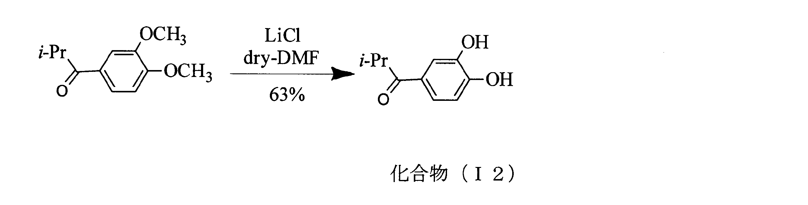
次に、100mL二口ナスフラスコに化合物(I1)を2.73g(13.1mmol)入れ、窒素雰囲気下でN,N-ジメチルホルムアミド乾燥溶媒(以下、「DMF」という。)50mL、塩化リチウム11.2g(262mmol:20eq)、を加えた。170℃で29時間還流し、100℃で32時間撹拌した。その後、飽和食塩水200mL、2規定の塩酸50mLを加え、酢酸エチル150mL×3回で抽出し、無水硫酸マグネシウムで乾燥、ろ過、濃縮、真空乾燥した。カラムクロマトグラフィー(ヘキサン:酢酸エチル=2:1)により単離精製し、濃縮、真空乾燥を行い黄色粘体(化合物(I2))1.50g(8.30mmol,63%)を得た。
上記合成で得られた化合物(化合物(I2))1-(3,4-ジヒドロキシフェニル)-2-メチルプロパノンの同定を以下に示す。
1H-NMR(400MHz,CDCl3):δ1.21(6H,d,J=6.8Hz),3.53(1H,sep,J=6.9Hz),6.35(1H,s),6.94(1H,d,J=8.4Hz),7.39 (1H,s),7.52(1H,d,J=8.4Hz),7.83 (1H,d,J=2.0Hz).
IR (NaCl):1656(C=O),3349(OH)cm-1.
1H-NMR(400MHz,CDCl3):δ1.21(6H,d,J=6.8Hz),3.53(1H,sep,J=6.9Hz),6.35(1H,s),6.94(1H,d,J=8.4Hz),7.39 (1H,s),7.52(1H,d,J=8.4Hz),7.83 (1H,d,J=2.0Hz).
IR (NaCl):1656(C=O),3349(OH)cm-1.
100mL二口ナスフラスコに化合物(I2)を1.02g(5.67mmol)、DMFを15mL、炭酸カリウムを1.57g(11.3mmol:2eq)入れ、室温で2時間撹拌した。その後、1-ヨード-1H,1H,2H,2H,3H,3H-パーフルオロヘプタン4.64g(12.0mmol:2.1eq)にDMF7mLを加え、滴下し、60℃で14時間撹拌した。反応溶液を減圧留去し、精製水60mL、2規定の塩酸20mLを加え、酢酸エチル(60mL×4)で抽出、飽和食塩水(60mL×5)で洗浄を行った。有機層を無水硫酸マグネシウムで乾燥し、ろ過、濃縮、真空乾燥を行い、橙色固体(化合物(I3))3.62g(5.17mmol,91%)を得た。
上記合成で得られた(化合物化合物(I3))1-(3,4-ジ(1H,1H,2H,2H,3H,3H-パーフルオロヘプチルオキシ)フェニル)-2-メチルプロパノンの同定を以下に示す。
1H-NMR(400MHz,CDCl3):δ1.21(6H,d,J=6.8Hz),2.15-2.19(4H,m),2.32-2.34(4H,m),3.53(1H,sep,J=6.9Hz),4.13and4.14 (4H,t,t),6.88 (1H,d,J=8.5Hz),7.52(1H,d,J=2.0Hz),7.58(1H,d,J=8.4Hz).
IR(KBr):722(CF3),1226(CF2,CF3),1678(C=O)cm-1.
1H-NMR(400MHz,CDCl3):δ1.21(6H,d,J=6.8Hz),2.15-2.19(4H,m),2.32-2.34(4H,m),3.53(1H,sep,J=6.9Hz),4.13and4.14 (4H,t,t),6.88 (1H,d,J=8.5Hz),7.52(1H,d,J=2.0Hz),7.58(1H,d,J=8.4Hz).
IR(KBr):722(CF3),1226(CF2,CF3),1678(C=O)cm-1.

100mLナスフラスコに化合物(I3)を0.502g(0.717mmol)を入れジエチルエーテル3mLで溶解し、氷浴中で70%硝酸5mLを少しずつ加え、氷浴中で1.5時間撹拌した。その後、氷に反応溶液を注ぎ、精製水50mL、 酢酸エチル(50mL×3)で抽出、5%炭酸水素ナトリウム(50mL×3)で洗浄を行った。有機層を無水硫酸マグネシウムで乾燥し、ろ過、濃縮した。濃縮したものをエタノール20mLで溶解し、再結晶を行った。結晶を吸引ろ過、真空乾燥を行い、薄黄色針状結晶(化合物(I4))0.256g(3.43mmol,48%)を得た。
上記合成で得られた化合物(化合物(I4))1-(2-ニトロ-4,5-ジ(1H,1H,2H,2H,3H,3H-パーフルオロヘプチルオキシ)フェニル)-2-メチルプロパノンの同定を以下に示す。
1H-NMR(400MHz,CDCl3):δ1.21(6H,d,J=6.8Hz),2.15-2.23(4H,m),2.27-2.34(4H,m),2.89(1H,sep),4.16and4.17(4H,t,t),6.67(1H,s),7.64(1H,s).
IR(KBr):721(CF3),1228(CF2,CF3),1358and1523(NO2),1703(C=O)cm-1.
1H-NMR(400MHz,CDCl3):δ1.21(6H,d,J=6.8Hz),2.15-2.23(4H,m),2.27-2.34(4H,m),2.89(1H,sep),4.16and4.17(4H,t,t),6.67(1H,s),7.64(1H,s).
IR(KBr):721(CF3),1228(CF2,CF3),1358and1523(NO2),1703(C=O)cm-1.

100mLナスフラスコに化合物(I4)を2.96g(3.97mmol)、テトラヒドロフラン12mL、メタノール8mLを入れ、氷浴中で水素化ホウ素ナトリウム0.300g(7.94mmol:2eq)を少しずつ加え90分間撹拌した。その後、室温で30分間撹拌した。反応溶液を濃縮し、精製水60mL、2規定の塩酸20mL、酢酸エチル(50mL×3)で抽出、有機層を無水硫酸マグネシウムで乾燥し、ろ過、濃縮した。カラムクロマトグラフィー(ヘキサン:酢酸エチル=6:1)により単離精製し、濃縮、真空乾燥を行い黄色粘体(化合物(I5))2.17g(2.90mmol,76%)を得た。
上記合成で得られた化合物(化合物(I5))1-(2-ニトロ-4,5-ジ(1H,1H,2H,2H,3H,3H-パーフルオロヘプチルオキシ)フェニル)-2-メチルプロパン-1-オールの同定を以下に示す。
1H-NMR(400MHz,CDCl3):δ0.94and0.96 (6H,d,d,J=6.8Hz),1.97-2.03(1H,m),2.14-2.21(5H,m),2.27-2.40(4H,m),4.08-4.23(4H,m),5.27(1H,t,J=4.8Hz),7.20(1H,s),7.55(1H,s).
IR(NaCl):742(CF3),1228(CF2,CF3),1334and1522(NO2),3547(OH)cm-1.
1H-NMR(400MHz,CDCl3):δ0.94and0.96 (6H,d,d,J=6.8Hz),1.97-2.03(1H,m),2.14-2.21(5H,m),2.27-2.40(4H,m),4.08-4.23(4H,m),5.27(1H,t,J=4.8Hz),7.20(1H,s),7.55(1H,s).
IR(NaCl):742(CF3),1228(CF2,CF3),1334and1522(NO2),3547(OH)cm-1.

窒素雰囲気下、100mLの二口ナスフラスコに(化合物(I5))1.43g(1.91mmol:1eq.)、トリエチルアミン0.580g(5.73mmol:3eq.)、ドライーアセトニトリル20mL、炭酸N-スクシンイミジル0.735g(2.87mmol:1.5eq.)を入れ、室温で40時間撹拌した。その後、反応溶液を濃縮し、精製水30mL、2規定の塩酸5mLを加え、酢酸エチル(30mL×3)で抽出、5%食塩水(30mL×3)で洗浄を行った。有機層を無水硫酸マグネシウムで乾燥し、ろ過、濃縮した。カラムクロマトグラフィー(ヘキサン:酢酸エチル=3:1)で単離精製し、濃縮、真空乾燥を行い黄色粘体(化合物(I6))1.55g(1.74mmol,91%)を得た。
上記合成で得られた化合物(化合物(I6))1-(2-ニトロ-4,5-ジ(1H,1H,2H,2H,3H,3H-パーフルオロヘプトキシ)フェニル)-2-メチルプロピル N-スクシンイミジルカーボネートの同定を以下に示す。
1H-NMR(400MHz,CDCl3):δ1.03and1.11(6H,d,d,J=7.2Hz),2.05-2.40(9H,m),2.79(4H,s),4.12-4.37(4H,m),6.38(1H,d,J=4.8Hz),6.96(1H,s),7.65(1H,s).
IR(NaCl):720(CF3),1227(CF2,CF3),1336and1524(NO2),1746(C=O)cm-1.
1H-NMR(400MHz,CDCl3):δ1.03and1.11(6H,d,d,J=7.2Hz),2.05-2.40(9H,m),2.79(4H,s),4.12-4.37(4H,m),6.38(1H,d,J=4.8Hz),6.96(1H,s),7.65(1H,s).
IR(NaCl):720(CF3),1227(CF2,CF3),1336and1524(NO2),1746(C=O)cm-1.

30mLの二口ナスフラスコに(化合物(I6))を0.603g(0.680mmol)、ドライーテトラヒドロフラン(以下、「THF」という。)を10mL、3-アミノプロピルトリメトキシシランを0.136g(0.759mmol:1.1eq)加え、室温で3.5時間撹拌した。反応溶液を濃縮し、中圧カラムクロマトグラフィー(ヘキサン:酢酸エチル:テトラメトキシシラン=3:1:0.04)で単離し、濃縮、真空乾燥をして、淡黄色固体(含フッ素化合物(1))0.451g(0.473mmol,70%)を得た。
上記合成で得られた含フッ素化合物(1)1-(2-ニトロ-4,5-ジ(1H,1H,2H,2H,3H,3H-パーフルオロヘプトキシ)フェニル)-2-メチルプロピルN-(3-トリメトキシシリル)プロピルカルバメートの同定を以下に示す。
1H-NMR(400MHz,CDCl3):δ0.58-0.67(2H,m),0.98(6H,dd,J=6.8,4.0Hz),1.56-1.63(2H,m),2.10-2.20(5H,m),2.26-2.41(4H,m),3.09-3.16(2H,m),3.56 (9H,s),4.10-4.15(4H,m),5.00(1H,t,J=5.8Hz),6.20(1H,d,J=5.2Hz),6.87(1H,s),7.57(1H,s).
IR(KBr):720(CF3),1227(CF2,CF3),1336and1524(NO2),1746(C=O)cm-1.
1H-NMR(400MHz,CDCl3):δ0.58-0.67(2H,m),0.98(6H,dd,J=6.8,4.0Hz),1.56-1.63(2H,m),2.10-2.20(5H,m),2.26-2.41(4H,m),3.09-3.16(2H,m),3.56 (9H,s),4.10-4.15(4H,m),5.00(1H,t,J=5.8Hz),6.20(1H,d,J=5.2Hz),6.87(1H,s),7.57(1H,s).
IR(KBr):720(CF3),1227(CF2,CF3),1336and1524(NO2),1746(C=O)cm-1.

≪合成例:含フッ素化合物(2)の合成≫
<1-(3,4-ビス((4,4,5,5,6,6,7,7,8,8,8-ウンデカフルオロオクチル)オキシ)フェニル)エタノンの合成(ステップ1)>
1-(3,4-ビス((4,4,5,5,6,6,7,7,8,8,8-ウンデカフルオロオクチル)オキシ)フェニル)エタノン(化合物(I21))を以下に示す工程で合成した。
100mL三口ナスフラスコに炭酸カリウム1.11g(8.03mmol)を量りとり、反応器内を窒素置換したDMF10mL、1-(3,4-ジヒドロキシフェニル)エタノン0.61g(4.01mmol)を加え室温で10分間撹拌した。その後、DMF8mLに溶解させた1,1,1,2,2,3,3,4,4,5,5,6,6-トリデカフルオロ-9-ヨードノネート4.00g(8.20mmol)を加え、滴下し、室温で24時間撹拌した。その後60℃に昇温し、1時間撹拌した。反応溶液を減圧留去し、精製水20mL、飽和塩化アンモニウム水溶液60ml、1.2規定塩酸40mLを加え、酢酸エチル(50mL×6)で抽出、飽和塩化ナトリウム水溶液(40mL×3)で洗浄を行った。有機層を無水硫酸ナトリウムで乾燥し、ろ過、濃縮、真空乾燥を行い白色固体(化合物(I21))3.46g(3.97mmol,99%)を得た。
上記合成で得られた化合物(化合物(I21))の同定を以下に示す。
1H-NMR(400MHz,CDCl3):δ(ppm)2.10-2.19(4H,m),2.26-2.40(4H,m),3.05(3H,s),4.12and4.13 (4H,t,t,J=7.2Hz),6.88 (1H,d,J=10.5Hz),7.50(1H,d,J=2.5Hz),7.56(1H,dd,J=2.5,14.8Hz).
13C-NMR(100MHz,CDCl3):δ(ppm)
20.63,26.29,27.88,67.35,111.64,112.21,123.69,130.91,148.35,152.74,196.78.
19F-NMR(376MHz,CDCl3):δ(ppm)-126.29(4F),-123.53(4F),-123.01(4F),-122.04(4F),-114.62(4F),-80.92(6F).

<1-(2-ニトロ-4,5-ビス((4,4,5,5,6,6,7,7,8,8,9,9,9-トリデカフルオロノニル)オキシ)フェニル)エタノンの合成(ステップ2)>
1-(2-ニトロ-4,5-ビス((4,4,5,5,6,6,7,7,8,8,9,9,9-トリデカフルオロノニル)オキシ)フェニル)エタノン(化合物(I22))を以下に示す工程で合成した。
50mLナスフラスコに1-(3,4-ビス((4,4,5,5,6,6,7,7,8,8,9,9,9-トリデカフルオロノニル)オキシ)フェニル)エタノン1.0g(1.15mmol)を入れ酢酸3mLで溶解させた。さらに酢酸2mlに溶解させた60%硝酸3mLを滴下し、50℃に昇温し4時間撹拌した。その後、反応器内に氷水を100ml加え、酢酸エチル(50mL×6)で抽出、飽和炭酸水素ナトリウム水溶液(50mL×3)で洗浄を行った。有機層を無水硫酸ナトリウムで乾燥し、ろ過、濃縮した。フラッシュカラムクロマトグラフィ(ヘキサン:酢酸エチル=5:1~0:1)により単離精製し、濃縮、真空乾燥を行い乳白色固体(化合物(I22))0.84g(0.92mmol,80%)を得た。
上記合成で得られた化合物(化合物(I22))の同定を以下に示す。
1H-NMR(400MHz,CDCl3):δ(ppm)2.15-2.21(4H,m),2.27-2.39(4H,m),2.48(3H,s),4.16and4.16(4H,t),6.64(1H,s),7.59(1H,s).
13C-NMR(100MHz,CDCl3):δ(ppm)20.46,27.68,30.47,67.80,108.15,109.78,133.16,138.65,148.82,153.29,199.93.
19F-NMR(376MHz,CDCl3):δ(ppm)-126.28(4F),-123.52(4F),-123.01(4F),-122.03(4F),-114.64(4F),-80.84(6F).

<1-(2-ニトロ-4,5-ビス((4,4,5,5,6,6,7,7,8,8,9,9,9-トリデカフルオロノニル)オキシ)フェニル)エタノールの合成(ステップ3)>
1-(2-ニトロ-4,5-ビス((4,4,5,5,6,6,7,7,8,8,9,9,9-トリデカフルオロノニル)オキシ)フェニル)エタノール(化合物(I23))を以下に示す工程で合成した。
50mLナスフラスコに水素化ホウ素ナトリウム0.080g(2.11mmol)、テトラヒドロフラン1mL、メタノール1mLを入5分間撹拌した。別容器でテトラヒドロフラン2mL、メタノール2mLに溶解させた1-(2-ニトロ-4,5-ビス((4,4,5,5,6,6,7,7,8,8,9,9,9-トリデカフルオロノニル)オキシ)フェニル)エタノン0.84g(0.92mmol)を、0℃下でゆっくりと滴下した。15分後室温に昇温し、45分間撹拌した。反応溶液を濃縮し、精製水5mL、飽和塩化アンモニウム水溶液20ml、酢酸エチル(50mL×4)で抽出、有機層を無水硫酸ナトリウムで乾燥し、ろ過、濃縮した。フラッシュカラムクロマトグラフィ(ヘキサン:酢酸エチル=10:1~3:1)により単離精製し、濃縮、真空乾燥を行い黄緑色粘体(化合物(I23))0.40g(0.43mmol,80%)を得た。
上記合成で得られた化合物(化合物(I23))の同定を以下に示す。
1H-NMR(400MHz,CDCl3):δ(ppm)2.12-2.20(4H,m),2.27-2.40(5H,m),4.10-4.20(3H,m),7.29(1H,s),7.55(1H,s).
13C-NMR(100MHz,CDCl3):δ(ppm)20.05,24.45,27.76,65.81,67.59,109.34,109.84,137.25,139.84,146.96,153.17.
19F-NMR(376MHz,CDCl3):δ(ppm)-126.27(4F),-123.52(4F),-123.00(4F),-122.02(4F),-114.62(4F),-80.86(6F).
1H-NMR(400MHz,CDCl3):δ(ppm)2.12-2.20(4H,m),2.27-2.40(5H,m),4.10-4.20(3H,m),7.29(1H,s),7.55(1H,s).
13C-NMR(100MHz,CDCl3):δ(ppm)20.05,24.45,27.76,65.81,67.59,109.34,109.84,137.25,139.84,146.96,153.17.
19F-NMR(376MHz,CDCl3):δ(ppm)-126.27(4F),-123.52(4F),-123.00(4F),-122.02(4F),-114.62(4F),-80.86(6F).

<1-(2-ニトロ-4,5-ビス((4,4,5,5,6,6,7,7,8,8,9,9,9-トリデカフルオロノニル)オキシ)フェニル)エチル(3-(トリエトキシシリル)プロピル)カルバメートの合成(ステップ4)>
1-(2-ニトロ-4,5-ビス((4,4,5,5,6,6,7,7,8,8,9,9,9-トリデカフルオロノニル)オキシ)フェニル)エチル(3-(トリエトキシシリル)プロピル)カルバメート(含フッ素化合物(2))を以下に示す工程で合成した。
30mLナスフラスコに窒素下で1-(2-ニトロ-4,5-ビス((4,4,5,5,6,6,7,7,8,8,9,9,9-トリデカフルオロノニル)オキシ)フェニル)エタノール0.24g(0.26mmol)、テトラヒドロフラン3mL、トリエトキシ(3-イソシアネートプロピル)シラン0.17g(0.71mmol)を加え、さらにテトラヒドロフラン2mLに溶解させたジブチルチンジラウレートを滴下した。室温で30分間撹拌した後、加熱還流させ21時間撹拌した。反応溶液を濃縮し、フラッシュシリカゲルカラムクロマトグラフィー(ヘキサン:酢酸エチル=10:1~3:1)で単離し、濃縮、真空乾燥をして、淡黄色固体(含フッ素化合物(2))0.29g(0.25mmol,93%)を得た。
上記合成で得られた化合物(含フッ素化合物(2))の同定を以下に示す。
1H-NMR(400MHz,CDCl3):δ(ppm)0.56-0.64(4H,m),1.18-1.24(12H,m),1.55-1.65(5H,m),2.11-2.19(4H,m),2.24-2.40(4H,m),3.05-3.50(2H,m),3.77-3.83(6H,m),4.08-4.16(4H,m),5.03(1H,t),.6.33(1H,q),6.97(1H,s),7.56(1H,s).
13C-NMR(100MHz,CDCl3):δ(ppm)7.67,18.13,20.49,22.14,23.20,27.72,43.34,58.42,67.53,67.65,68.55,109.45,109.54,134.63,140.06,147.10,152.95,155.23.
19F-NMR(376MHz,CDCl3):δ(ppm)-126.27(4F),-123.54(4F),-123.01(4F),-122.03(4F),-114.64(4F),-80.88(6F).

以下に、1-(2-ニトロ-4,5-ビス((4,4,5,5,6,6,7,7,8,8,9,9,9-トリデカフルオロフェニル)オキシ)フェニル)エチル(3-(トリエトキシシリル)プロピル)カルバメート(含フッ素化合物(2))の合成経路を示す。

上記≪合成例:含フッ素化合物(1)の合成≫と同法の方法により、下記の含フッ素化合物(3)を得た。

≪含フッ素組成物による基板の表面修飾≫
上記の合成方法によって得られた、含フッ素化合物(1)~(3)を用いて含フッ素組成物(1)~(3)を調製し、該含フッ素組成物(1)~(3)を用いて基板の表面修飾を行った。
上記の合成方法によって得られた、含フッ素化合物(1)~(3)を用いて含フッ素組成物(1)~(3)を調製し、該含フッ素組成物(1)~(3)を用いて基板の表面修飾を行った。
[含フッ素組成物の調製]
50mLナスフラスコに、20mLの1,3-ビス(トリフルオロメチル)ベンゼン(以下、「HFX」と記載することがある。)と、上記で得た含フッ素化合物(1)~(3)をそれぞれ入れ、0.1mMの含フッ素組成物(1)~(3)を調製した。
また、50mLナスフラスコに、20mLのトルエンと、上記で得た含フッ素化合物(1)~(2)をそれぞれ入れ、0.1mMの含フッ素組成物(4)~(5)を調製した。
下記表1に、含フッ素組成物(1)~(5)をまとめて記載する。
50mLナスフラスコに、20mLの1,3-ビス(トリフルオロメチル)ベンゼン(以下、「HFX」と記載することがある。)と、上記で得た含フッ素化合物(1)~(3)をそれぞれ入れ、0.1mMの含フッ素組成物(1)~(3)を調製した。
また、50mLナスフラスコに、20mLのトルエンと、上記で得た含フッ素化合物(1)~(2)をそれぞれ入れ、0.1mMの含フッ素組成物(4)~(5)を調製した。
下記表1に、含フッ素組成物(1)~(5)をまとめて記載する。

[基板前処理]
熱酸化膜付きシリコンウェハをメタノール、水、アセトンでそれぞれ5分間超音波洗浄した。基板を取り出し窒素気流で乾燥させ、UVオゾンクリーナーで前処理した。UVオゾンクリーナーの酸素注入は流量6L/minで3分間注入し、UV照射は1.5時間とし、生じたオゾンは窒素を流量6L/minで10分間流して排出した。
熱酸化膜付きシリコンウェハをメタノール、水、アセトンでそれぞれ5分間超音波洗浄した。基板を取り出し窒素気流で乾燥させ、UVオゾンクリーナーで前処理した。UVオゾンクリーナーの酸素注入は流量6L/minで3分間注入し、UV照射は1.5時間とし、生じたオゾンは窒素を流量6L/minで10分間流して排出した。
[基板表面修飾]
前処理した基板を、含フッ素組成物(1)、(3)~(5)にそれぞれ浸漬し、窒素下で100℃に加熱し、24時間静置した。
基板を取り出してメタノールで洗い、メタノール中で超音波洗浄(10分間)を行った。さらに、クロロホルムで洗い、クロロホルム中で超音波洗浄(10分間)を行った。その後、表面を窒素で乾燥させた。
基板表面修飾は、下記のように行われたと考えられる。
前処理した基板を、含フッ素組成物(1)、(3)~(5)にそれぞれ浸漬し、窒素下で100℃に加熱し、24時間静置した。
基板を取り出してメタノールで洗い、メタノール中で超音波洗浄(10分間)を行った。さらに、クロロホルムで洗い、クロロホルム中で超音波洗浄(10分間)を行った。その後、表面を窒素で乾燥させた。
基板表面修飾は、下記のように行われたと考えられる。

≪修飾基板への光照射≫
その後、得られた修飾基板の光分解性を調べるために、超高圧水銀灯で、320nm以下の波長の光を遮断する硫酸銅フィルターを通して、照度25mW/cm2で光照射した。光照射した基板をメタノール、クロロホルムで洗い流し、クロロホルムで5分間超音波洗浄し、窒素気流で乾燥した。
光分解は次式のようになされ、光照射するとニトロベンジル基の光分解によりニトロソ化合物が脱離し、基板表面にアミノ基を導入できる。
その後、得られた修飾基板の光分解性を調べるために、超高圧水銀灯で、320nm以下の波長の光を遮断する硫酸銅フィルターを通して、照度25mW/cm2で光照射した。光照射した基板をメタノール、クロロホルムで洗い流し、クロロホルムで5分間超音波洗浄し、窒素気流で乾燥した。
光分解は次式のようになされ、光照射するとニトロベンジル基の光分解によりニトロソ化合物が脱離し、基板表面にアミノ基を導入できる。

得られた修飾基板について、拡張収縮法により、水の接触角(静的(θS)、前進(θA)、後退(θR))、ぬれのヒステリシス(Δθ)を測定した。
加えて、得られた修飾基板について、原子間力顕微鏡(AFM)により平均表面粗さ(Ra)を測定した。その結果を表2に示す。
加えて、得られた修飾基板について、原子間力顕微鏡(AFM)により平均表面粗さ(Ra)を測定した。その結果を表2に示す。

表2に記載したとおり、拡張収縮法による前進後退接触角の差から求めたぬれのヒステリシスの低下と、表面粗さ(Ra)の結果から、溶剤にトルエンを用いた含フッ素組成物(4)又は(5)よりも、フッ素系溶剤(HFX)を用いた含フッ素組成物(1)又は(3)を用いたほうが、平滑な単分子膜となっていることが確認できた。
比較例1~2では、撥水性・撥油性の高いフッ素化アルキル基を有する含フッ素化合物(1)又は(3)は、トルエン溶液中では均一に溶解しておらず、凝集体として存在していたため、平滑な単分子膜が形成できない要因となっていたと推察される。
一方、フッ素系溶剤を用いた実施例1~2は、フッ素化アルキル基を有する含フッ素化合物が溶剤中で凝集せず、均一に分散したため、平滑な単分子膜を形成することができたと推察される。
ここで、上述の実施形態で説明したトランジスタを製造する場合、各層を基板側から順に積層して作製するため、含フッ素組成物に起因する表面粗さはその上に形成される電極にも反映される。電極が凹凸形状を有していれば、ゲート電極と、ソース電極(またはドレイン電極)とのリーク等、トランジスタの性能を低下させるおそれがあるが、表2のとおり本実施例の含フッ素組成物を用いた薄膜は表面粗さ(Ra)が小さいためトランジスタの製造に好適に使用することができる。
≪単分子膜形成試験≫
実施例1~2において形成された膜について、単分子膜が形成されていることを確認するため、X線光電子分光法(X-ray photoelectron spectroscopy,以下、「XPS」という。)、X線反射率法(X-ray Reflectometer,以下「XRR」という。)による角度分解分析により膜厚を求めた。その結果を表3に記載する。
ChemBioDraw Ultra12.0により算出した計算値も併せて表3に「Calc.」として記載する。
実施例1~2において形成された膜について、単分子膜が形成されていることを確認するため、X線光電子分光法(X-ray photoelectron spectroscopy,以下、「XPS」という。)、X線反射率法(X-ray Reflectometer,以下「XRR」という。)による角度分解分析により膜厚を求めた。その結果を表3に記載する。
ChemBioDraw Ultra12.0により算出した計算値も併せて表3に「Calc.」として記載する。

表3に記載したとおり、XRRとXPSにより求めた膜厚が、ChemBioDraw Ultra12.0により算出した計算値による膜厚とほぼ一致していることから、フッ素系溶剤を用いた場合であっても、単分子膜が形成されていることが確認できた。
≪インク塗布試験≫
3インチシリコンウェハをメタノール、純水、アセトンでそれぞれ5分間超音波洗浄した。基板を取り出し窒素気流で乾燥させ、UVオゾンクリーナーで、シリコンウェハは鏡面にUVを1.5時間照射し、オゾンクリーナーの酸素注入は流量6L/minで3分間注入し、UV照射は1.5時間とし、生じたオゾンは窒素を流量6L/minで10分間流して排出した。
3インチシリコンウェハをメタノール、純水、アセトンでそれぞれ5分間超音波洗浄した。基板を取り出し窒素気流で乾燥させ、UVオゾンクリーナーで、シリコンウェハは鏡面にUVを1.5時間照射し、オゾンクリーナーの酸素注入は流量6L/minで3分間注入し、UV照射は1.5時間とし、生じたオゾンは窒素を流量6L/minで10分間流して排出した。
含フッ素組成物(1)~(3)を前記と同様に調製し、前処理済みの基板をこのセパラブルフラスコ中、窒素下で100℃に加熱し、24時間浸漬させた。基板をメタノールで洗浄し、メタノール、クロロホルムで各10分間超音波洗浄し、窒素気流で乾燥した。
これら基板を用いて含フッ素組成物(1)~(3)における長鎖フルオロアルキル基の有効性を評価した。
これら基板を用いて含フッ素組成物(1)~(3)における長鎖フルオロアルキル基の有効性を評価した。
含フッ素組成物(1)~(3)を用いて形成したSAM膜(各感光性アミン発生層)を作製した基板に様々なL/Sが描画されたフォトマスク(L/S=400/400um, 200/200um, 100um/100um, 50/50um, 30/30um, 10/10um, 5/5um, 3/3um)を介して、波長365nm光を照度43 mW/cm2の光を46.5秒間(2.0J/cm2)照射した。光照射後、基板をクロロホルム中で超音波洗浄を3分間行い、窒素気流で表面を乾燥させた。
各基板に3mlのAgナノインク(株式会社コロイダルインク社製Drycure Ag)をスピンコート(3000rpm)で成膜し、室温で乾燥させた。露光部に優先して金属配線を形成できるため、そのパターンの形成結果を光学顕微鏡で観察した。
含フッ素組成物(1)~(3)における長鎖フルオロアルキル基の有効性判断については、各基板L/S=50/50umの同領域を観察し、「L(ライン部)にのみ金属Agが配線できていること、LとLをまたがるようにS(スペース部)に金属Ag存在しないこと」を基準としてもうけた。その結果を表4に示す。
表4中、「○」は、L(ライン部)にのみ金属Agが配線できており、LとLをまたがるようにS(スペース部)が形成され、S部に金属Agが存在していなかったことを示す。
表4中、「△」は、L(ライン部)にのみ金属Agが配線できており、LとLをまたがるようにS(スペース部)が形成されているが、一部のS部に金属Agがあり、パターンが連結した部分が観察されたことを示す。

上記結果に示したとおり、本実施例の含フッ素組成物を用いて基板表面を修飾し、新水性/撥水性パターンを形成した基板は、銀インクを良好に塗布することができた。
さらに、長鎖フッ素化アルキル基を有する含フッ素化合物を含む含フッ素組成物のほうが、良好にパターンを形成することができた。この結果から、長鎖フルオロアルキル基の導入が材料のパターニングおいて有効な選択性を示す手段であると判断した。
さらに、長鎖フッ素化アルキル基を有する含フッ素化合物を含む含フッ素組成物のほうが、良好にパターンを形成することができた。この結果から、長鎖フルオロアルキル基の導入が材料のパターニングおいて有効な選択性を示す手段であると判断した。
S…基板 CONT…制御部 Sa…被処理面 2…基板供給部 3…基板処理部 4…基板回収部 6…含フッ素組成物塗布部 7…露光部 8…マスク 9…パターン材料塗布部 100…基板処理装置
Claims (9)
- 下記一般式(1)で表される含フッ素化合物と、フッ素系溶剤と、を含有する含フッ素組成物。

Xはハロゲン原子又はアルコキシ基を表し、
R1は水素原子又は炭素数1~10の直鎖状、分岐鎖状又は環状のアルキル基を表し、
Rf1、Rf2はそれぞれ独立にフッ素化アルコキシ基であって、
nは0以上の整数を表す。] - 請求項1に記載の含フッ素組成物を用いて化学修飾された表面を有するパターン形成用基板。
- 請求項1に記載の含フッ素組成物からなることを特徴とする光分解性カップリング剤。
- 対象物の被処理面にパターンを形成する方法であって、
請求項1に記載の含フッ素組成物を用いて、前記被処理面を化学修飾する第1の工程と、
化学修飾された前記被処理面を露光し、親水領域及び撥水領域からなる潜像を生成させる第2の工程と、
前記親水領域又は撥水領域にパターン形成材料を配置させる第3の工程と、
を含むパターン形成方法。 - 可撓性の基板の上に電子デバイス用の回路パターンを形成する方法であって、
前記基板の表面の全体、または特定の領域内を、請求項1に記載の含フッ素組成物を用いて化学修飾する第1の工程と、
前記化学修飾された前記基板の表面を露光し、前記基板の表面に、親撥水性の違いによる前記回路パターンの潜像を生成させる第2の工程と、
前記基板の表面の前記潜像の部分に流動性のパターン形成材料を接触させ、前記親撥水性の違いによって前記パターン形成材料を前記回路パターンの形状で前記基板上に捕捉させる第3の工程と、
を含むパターン形成方法。 - 前記パターン形成材料は、液状の導電材料、液状の半導体材料、又は液状の絶縁材料を含む請求項4又は5に記載のパターン形成方法。
- 所定の基板の上に電子デバイス用の回路パターンを形成する方法であって、
請求項1に記載の含フッ素組成物を前記基板上に塗布して、含フッ素組成物層を形成する工程と、
前記基板上に形成された前記含フッ素組成物層を所定のパターン光で露光し、前記基板上に親撥水性の違いによる前記回路パターンの潜像を形成する工程と、
前記潜像部分に無電解めっき用触媒を接触させ、無電解めっきを行う工程と、
を含むパターン形成方法。 - 前記露光時に照射する光は、200nm~450nmの波長域に含まれる光を含む請求項4~7のいずれか1項に記載のパターン形成方法。
- ゲート電極と、ソース電極と、ドレイン電極と、を有するトランジスタの製造方法であって、
前記ゲート電極、前記ソース電極、前記ドレイン電極のうち少なくとも1つの電極を、請求項5~8のいずれか1項に記載のパターン形成方法で形成する工程を含むトランジスタの製造方法。
Priority Applications (1)
| Application Number | Priority Date | Filing Date | Title |
|---|---|---|---|
| US15/629,222 US10466591B2 (en) | 2015-02-25 | 2017-06-21 | Fluorine-containing composition, substrate for pattern formation, photodegradable coupling agent, pattern formation method and transistor production method |
Applications Claiming Priority (4)
| Application Number | Priority Date | Filing Date | Title |
|---|---|---|---|
| JP2015035424 | 2015-02-25 | ||
| JP2015-035424 | 2015-02-25 | ||
| JP2016-027241 | 2016-02-16 | ||
| JP2016027241A JP6640593B2 (ja) | 2015-02-25 | 2016-02-16 | 含フッ素組成物、パターン形成用基板、光分解性カップリング剤、パターン形成方法及びトランジスタの製造方法 |
Related Child Applications (1)
| Application Number | Title | Priority Date | Filing Date |
|---|---|---|---|
| US15/629,222 Continuation US10466591B2 (en) | 2015-02-25 | 2017-06-21 | Fluorine-containing composition, substrate for pattern formation, photodegradable coupling agent, pattern formation method and transistor production method |
Publications (1)
| Publication Number | Publication Date |
|---|---|
| WO2016136817A1 true WO2016136817A1 (ja) | 2016-09-01 |
Family
ID=56788932
Family Applications (1)
| Application Number | Title | Priority Date | Filing Date |
|---|---|---|---|
| PCT/JP2016/055456 WO2016136817A1 (ja) | 2015-02-25 | 2016-02-24 | 含フッ素組成物、パターン形成用基板、光分解性カップリング剤、パターン形成方法及びトランジスタの製造方法 |
Country Status (1)
| Country | Link |
|---|---|
| WO (1) | WO2016136817A1 (ja) |
Cited By (3)
| Publication number | Priority date | Publication date | Assignee | Title |
|---|---|---|---|---|
| JP2018123082A (ja) * | 2017-01-31 | 2018-08-09 | 株式会社ニコン | 化合物、パターン形成用基板、光分解性カップリング剤、パターン形成方法及びトランジスタの製造方法 |
| WO2019131290A1 (ja) * | 2017-12-25 | 2019-07-04 | Agc株式会社 | 金属パターン付き基材の製造方法 |
| WO2020100710A1 (ja) * | 2018-11-16 | 2020-05-22 | 株式会社ニコン | パターン形成方法、トランジスタの製造方法及びパターン形成用フィルム |
Citations (7)
| Publication number | Priority date | Publication date | Assignee | Title |
|---|---|---|---|---|
| JPH06248256A (ja) * | 1993-02-24 | 1994-09-06 | Asahi Glass Co Ltd | 溶剤型表面改質剤組成物 |
| JP2003321479A (ja) * | 2002-05-02 | 2003-11-11 | Japan Science & Technology Corp | 光分解性シランカップリング剤 |
| WO2005054256A1 (ja) * | 2003-12-04 | 2005-06-16 | Asahi Glass Company, Limited | 含フッ素化合物、撥水性組成物および薄膜 |
| JP2008096596A (ja) * | 2006-10-10 | 2008-04-24 | Canon Inc | パターン形成方法 |
| WO2012036053A1 (ja) * | 2010-09-14 | 2012-03-22 | セントラル硝子株式会社 | 防汚性物品及びその製造方法、並びに防汚層形成用塗布剤 |
| JP2013244470A (ja) * | 2012-05-28 | 2013-12-09 | Shin-Etsu Chemical Co Ltd | 含フッ素ドライコーティング剤のコーティング方法 |
| WO2015029981A1 (ja) * | 2013-08-27 | 2015-03-05 | 学校法人神奈川大学 | 含フッ素化合物、パターン形成用基板、光分解性カップリング剤、パターン形成方法、化合物 |
-
2016
- 2016-02-24 WO PCT/JP2016/055456 patent/WO2016136817A1/ja active Application Filing
Patent Citations (7)
| Publication number | Priority date | Publication date | Assignee | Title |
|---|---|---|---|---|
| JPH06248256A (ja) * | 1993-02-24 | 1994-09-06 | Asahi Glass Co Ltd | 溶剤型表面改質剤組成物 |
| JP2003321479A (ja) * | 2002-05-02 | 2003-11-11 | Japan Science & Technology Corp | 光分解性シランカップリング剤 |
| WO2005054256A1 (ja) * | 2003-12-04 | 2005-06-16 | Asahi Glass Company, Limited | 含フッ素化合物、撥水性組成物および薄膜 |
| JP2008096596A (ja) * | 2006-10-10 | 2008-04-24 | Canon Inc | パターン形成方法 |
| WO2012036053A1 (ja) * | 2010-09-14 | 2012-03-22 | セントラル硝子株式会社 | 防汚性物品及びその製造方法、並びに防汚層形成用塗布剤 |
| JP2013244470A (ja) * | 2012-05-28 | 2013-12-09 | Shin-Etsu Chemical Co Ltd | 含フッ素ドライコーティング剤のコーティング方法 |
| WO2015029981A1 (ja) * | 2013-08-27 | 2015-03-05 | 学校法人神奈川大学 | 含フッ素化合物、パターン形成用基板、光分解性カップリング剤、パターン形成方法、化合物 |
Non-Patent Citations (1)
| Title |
|---|
| KONISHI ET AL.: "Kobunkaisei Carbamate-gata Silane Coupling-zai 1", THE 62ND SYMPOSIUM ON MACROMOLECULES YOKOSHU, 28 August 2013 (2013-08-28), pages 3723 * |
Cited By (8)
| Publication number | Priority date | Publication date | Assignee | Title |
|---|---|---|---|---|
| JP2018123082A (ja) * | 2017-01-31 | 2018-08-09 | 株式会社ニコン | 化合物、パターン形成用基板、光分解性カップリング剤、パターン形成方法及びトランジスタの製造方法 |
| WO2018143173A1 (ja) * | 2017-01-31 | 2018-08-09 | 株式会社ニコン | 化合物、パターン形成用基板、光分解性カップリング剤、パターン形成方法及びトランジスタの製造方法 |
| WO2019131290A1 (ja) * | 2017-12-25 | 2019-07-04 | Agc株式会社 | 金属パターン付き基材の製造方法 |
| CN111527799A (zh) * | 2017-12-25 | 2020-08-11 | Agc株式会社 | 带金属图案的基材的制造方法 |
| JPWO2019131290A1 (ja) * | 2017-12-25 | 2021-01-21 | Agc株式会社 | 金属パターン付き基材の製造方法 |
| CN111527799B (zh) * | 2017-12-25 | 2023-09-26 | Agc株式会社 | 带金属图案的基材的制造方法 |
| JP7392472B2 (ja) | 2017-12-25 | 2023-12-06 | Agc株式会社 | 金属パターン付き基材の製造方法、及びそれに用いる組成物 |
| WO2020100710A1 (ja) * | 2018-11-16 | 2020-05-22 | 株式会社ニコン | パターン形成方法、トランジスタの製造方法及びパターン形成用フィルム |
Similar Documents
| Publication | Publication Date | Title |
|---|---|---|
| JP6640593B2 (ja) | 含フッ素組成物、パターン形成用基板、光分解性カップリング剤、パターン形成方法及びトランジスタの製造方法 | |
| US11518731B2 (en) | Fluorine-containing compound, substrate for patterning, photodegradable coupling agent, patterning method, and compound | |
| WO2016136817A1 (ja) | 含フッ素組成物、パターン形成用基板、光分解性カップリング剤、パターン形成方法及びトランジスタの製造方法 | |
| US9606437B2 (en) | Fluorine-containing compound, substrate for pattern formation, photodegradable coupling agent, pattern formation method, and compound | |
| JP7121505B2 (ja) | 化合物、パターン形成用基板、光分解性カップリング剤、パターン形成方法及びトランジスタの製造方法 | |
| JP6548572B2 (ja) | パターン形成方法及び対象物の被処理面の改質方法 | |
| TWI788477B (zh) | 圖案形成方法、電晶體之製作方法及圖案形成用之構件 | |
| US20210184143A1 (en) | Transistor production method | |
| WO2018143173A1 (ja) | 化合物、パターン形成用基板、光分解性カップリング剤、パターン形成方法及びトランジスタの製造方法 | |
| WO2020194588A1 (ja) | パターン形成方法 | |
| JP6298989B2 (ja) | 含フッ素化合物、パタ−ン形成用基板、光分解性カップリング剤、パタ−ン形成方法、化合物、有機薄膜トランジスタ | |
| WO2019073878A1 (ja) | 化合物、パターン形成用基板、光分解性カップリング剤、パターン形成方法及びトランジスタの製造方法 | |
| WO2020045078A1 (ja) | トランジスタの製造方法 | |
| WO2020100710A1 (ja) | パターン形成方法、トランジスタの製造方法及びパターン形成用フィルム | |
| JP2019019092A (ja) | 化合物、パターン形成用基板、カップリング剤及びパターン形成方法 |
Legal Events
| Date | Code | Title | Description |
|---|---|---|---|
| 121 | Ep: the epo has been informed by wipo that ep was designated in this application |
Ref document number: 16755561 Country of ref document: EP Kind code of ref document: A1 |
|
| NENP | Non-entry into the national phase |
Ref country code: DE |
|
| 122 | Ep: pct application non-entry in european phase |
Ref document number: 16755561 Country of ref document: EP Kind code of ref document: A1 |