WO2016136348A1 - ガラス基板及びこれを用いた積層体 - Google Patents
ガラス基板及びこれを用いた積層体 Download PDFInfo
- Publication number
- WO2016136348A1 WO2016136348A1 PCT/JP2016/051932 JP2016051932W WO2016136348A1 WO 2016136348 A1 WO2016136348 A1 WO 2016136348A1 JP 2016051932 W JP2016051932 W JP 2016051932W WO 2016136348 A1 WO2016136348 A1 WO 2016136348A1
- Authority
- WO
- WIPO (PCT)
- Prior art keywords
- glass substrate
- glass
- less
- dots
- substrate
- Prior art date
- Legal status (The legal status is an assumption and is not a legal conclusion. Google has not performed a legal analysis and makes no representation as to the accuracy of the status listed.)
- Ceased
Links
Images







Classifications
-
- C—CHEMISTRY; METALLURGY
- C03—GLASS; MINERAL OR SLAG WOOL
- C03B—MANUFACTURE, SHAPING, OR SUPPLEMENTARY PROCESSES
- C03B17/00—Forming molten glass by flowing-out, pushing-out, extruding or drawing downwardly or laterally from forming slits or by overflowing over lips
- C03B17/06—Forming glass sheets
- C03B17/064—Forming glass sheets by the overflow downdraw fusion process; Isopipes therefor
-
- B—PERFORMING OPERATIONS; TRANSPORTING
- B23—MACHINE TOOLS; METAL-WORKING NOT OTHERWISE PROVIDED FOR
- B23K—SOLDERING OR UNSOLDERING; WELDING; CLADDING OR PLATING BY SOLDERING OR WELDING; CUTTING BY APPLYING HEAT LOCALLY, e.g. FLAME CUTTING; WORKING BY LASER BEAM
- B23K26/00—Working by laser beam, e.g. welding, cutting or boring
- B23K26/0006—Working by laser beam, e.g. welding, cutting or boring taking account of the properties of the material involved
-
- B—PERFORMING OPERATIONS; TRANSPORTING
- B23—MACHINE TOOLS; METAL-WORKING NOT OTHERWISE PROVIDED FOR
- B23K—SOLDERING OR UNSOLDERING; WELDING; CLADDING OR PLATING BY SOLDERING OR WELDING; CUTTING BY APPLYING HEAT LOCALLY, e.g. FLAME CUTTING; WORKING BY LASER BEAM
- B23K26/00—Working by laser beam, e.g. welding, cutting or boring
- B23K26/02—Positioning or observing the workpiece, e.g. with respect to the point of impact; Aligning, aiming or focusing the laser beam
- B23K26/06—Shaping the laser beam, e.g. by masks or multi-focusing
- B23K26/062—Shaping the laser beam, e.g. by masks or multi-focusing by direct control of the laser beam
- B23K26/0622—Shaping the laser beam, e.g. by masks or multi-focusing by direct control of the laser beam by shaping pulses
-
- B—PERFORMING OPERATIONS; TRANSPORTING
- B23—MACHINE TOOLS; METAL-WORKING NOT OTHERWISE PROVIDED FOR
- B23K—SOLDERING OR UNSOLDERING; WELDING; CLADDING OR PLATING BY SOLDERING OR WELDING; CUTTING BY APPLYING HEAT LOCALLY, e.g. FLAME CUTTING; WORKING BY LASER BEAM
- B23K26/00—Working by laser beam, e.g. welding, cutting or boring
- B23K26/352—Working by laser beam, e.g. welding, cutting or boring for surface treatment
- B23K26/355—Texturing
-
- B—PERFORMING OPERATIONS; TRANSPORTING
- B23—MACHINE TOOLS; METAL-WORKING NOT OTHERWISE PROVIDED FOR
- B23K—SOLDERING OR UNSOLDERING; WELDING; CLADDING OR PLATING BY SOLDERING OR WELDING; CUTTING BY APPLYING HEAT LOCALLY, e.g. FLAME CUTTING; WORKING BY LASER BEAM
- B23K26/00—Working by laser beam, e.g. welding, cutting or boring
- B23K26/352—Working by laser beam, e.g. welding, cutting or boring for surface treatment
- B23K26/359—Working by laser beam, e.g. welding, cutting or boring for surface treatment by providing a line or line pattern, e.g. a dotted break initiation line
-
- B—PERFORMING OPERATIONS; TRANSPORTING
- B23—MACHINE TOOLS; METAL-WORKING NOT OTHERWISE PROVIDED FOR
- B23K—SOLDERING OR UNSOLDERING; WELDING; CLADDING OR PLATING BY SOLDERING OR WELDING; CUTTING BY APPLYING HEAT LOCALLY, e.g. FLAME CUTTING; WORKING BY LASER BEAM
- B23K26/00—Working by laser beam, e.g. welding, cutting or boring
- B23K26/60—Preliminary treatment
-
- B—PERFORMING OPERATIONS; TRANSPORTING
- B32—LAYERED PRODUCTS
- B32B—LAYERED PRODUCTS, i.e. PRODUCTS BUILT-UP OF STRATA OF FLAT OR NON-FLAT, e.g. CELLULAR OR HONEYCOMB, FORM
- B32B17/00—Layered products essentially comprising sheet glass, or glass, slag, or like fibres
- B32B17/06—Layered products essentially comprising sheet glass, or glass, slag, or like fibres comprising glass as the main or only constituent of a layer, next to another layer of a specific material
-
- C—CHEMISTRY; METALLURGY
- C03—GLASS; MINERAL OR SLAG WOOL
- C03C—CHEMICAL COMPOSITION OF GLASSES, GLAZES OR VITREOUS ENAMELS; SURFACE TREATMENT OF GLASS; SURFACE TREATMENT OF FIBRES OR FILAMENTS MADE FROM GLASS, MINERALS OR SLAGS; JOINING GLASS TO GLASS OR OTHER MATERIALS
- C03C19/00—Surface treatment of glass, not in the form of fibres or filaments, by mechanical means
-
- C—CHEMISTRY; METALLURGY
- C03—GLASS; MINERAL OR SLAG WOOL
- C03C—CHEMICAL COMPOSITION OF GLASSES, GLAZES OR VITREOUS ENAMELS; SURFACE TREATMENT OF GLASS; SURFACE TREATMENT OF FIBRES OR FILAMENTS MADE FROM GLASS, MINERALS OR SLAGS; JOINING GLASS TO GLASS OR OTHER MATERIALS
- C03C23/00—Other surface treatment of glass not in the form of fibres or filaments
- C03C23/0005—Other surface treatment of glass not in the form of fibres or filaments by irradiation
- C03C23/001—Other surface treatment of glass not in the form of fibres or filaments by irradiation by infrared light
-
- C—CHEMISTRY; METALLURGY
- C03—GLASS; MINERAL OR SLAG WOOL
- C03C—CHEMICAL COMPOSITION OF GLASSES, GLAZES OR VITREOUS ENAMELS; SURFACE TREATMENT OF GLASS; SURFACE TREATMENT OF FIBRES OR FILAMENTS MADE FROM GLASS, MINERALS OR SLAGS; JOINING GLASS TO GLASS OR OTHER MATERIALS
- C03C23/00—Other surface treatment of glass not in the form of fibres or filaments
- C03C23/0005—Other surface treatment of glass not in the form of fibres or filaments by irradiation
- C03C23/0025—Other surface treatment of glass not in the form of fibres or filaments by irradiation by a laser beam
-
- H—ELECTRICITY
- H10—SEMICONDUCTOR DEVICES; ELECTRIC SOLID-STATE DEVICES NOT OTHERWISE PROVIDED FOR
- H10P—GENERIC PROCESSES OR APPARATUS FOR THE MANUFACTURE OR TREATMENT OF DEVICES COVERED BY CLASS H10
- H10P52/00—Grinding, lapping or polishing of wafers, substrates or parts of devices
-
- H—ELECTRICITY
- H10—SEMICONDUCTOR DEVICES; ELECTRIC SOLID-STATE DEVICES NOT OTHERWISE PROVIDED FOR
- H10P—GENERIC PROCESSES OR APPARATUS FOR THE MANUFACTURE OR TREATMENT OF DEVICES COVERED BY CLASS H10
- H10P90/00—Preparation of wafers not covered by a single main group of this subclass, e.g. wafer reinforcement
-
- H—ELECTRICITY
- H10—SEMICONDUCTOR DEVICES; ELECTRIC SOLID-STATE DEVICES NOT OTHERWISE PROVIDED FOR
- H10P—GENERIC PROCESSES OR APPARATUS FOR THE MANUFACTURE OR TREATMENT OF DEVICES COVERED BY CLASS H10
- H10P95/00—Generic processes or apparatus for manufacture or treatments not covered by the other groups of this subclass
-
- H—ELECTRICITY
- H10—SEMICONDUCTOR DEVICES; ELECTRIC SOLID-STATE DEVICES NOT OTHERWISE PROVIDED FOR
- H10W—GENERIC PACKAGES, INTERCONNECTIONS, CONNECTORS OR OTHER CONSTRUCTIONAL DETAILS OF DEVICES COVERED BY CLASS H10
- H10W70/00—Package substrates; Interposers; Redistribution layers [RDL]
- H10W70/60—Insulating or insulated package substrates; Interposers; Redistribution layers
- H10W70/67—Insulating or insulated package substrates; Interposers; Redistribution layers characterised by their insulating layers or insulating parts
- H10W70/69—Insulating materials thereof
- H10W70/692—Ceramics or glasses
-
- H—ELECTRICITY
- H10—SEMICONDUCTOR DEVICES; ELECTRIC SOLID-STATE DEVICES NOT OTHERWISE PROVIDED FOR
- H10W—GENERIC PACKAGES, INTERCONNECTIONS, CONNECTORS OR OTHER CONSTRUCTIONAL DETAILS OF DEVICES COVERED BY CLASS H10
- H10W72/00—Interconnections or connectors in packages
- H10W72/01—Manufacture or treatment
- H10W72/0198—Manufacture or treatment batch processes
-
- H—ELECTRICITY
- H10—SEMICONDUCTOR DEVICES; ELECTRIC SOLID-STATE DEVICES NOT OTHERWISE PROVIDED FOR
- H10W—GENERIC PACKAGES, INTERCONNECTIONS, CONNECTORS OR OTHER CONSTRUCTIONAL DETAILS OF DEVICES COVERED BY CLASS H10
- H10W74/00—Encapsulations, e.g. protective coatings
-
- H—ELECTRICITY
- H10—SEMICONDUCTOR DEVICES; ELECTRIC SOLID-STATE DEVICES NOT OTHERWISE PROVIDED FOR
- H10W—GENERIC PACKAGES, INTERCONNECTIONS, CONNECTORS OR OTHER CONSTRUCTIONAL DETAILS OF DEVICES COVERED BY CLASS H10
- H10W74/00—Encapsulations, e.g. protective coatings
- H10W74/01—Manufacture or treatment
- H10W74/014—Manufacture or treatment using batch processing
-
- H—ELECTRICITY
- H10—SEMICONDUCTOR DEVICES; ELECTRIC SOLID-STATE DEVICES NOT OTHERWISE PROVIDED FOR
- H10W—GENERIC PACKAGES, INTERCONNECTIONS, CONNECTORS OR OTHER CONSTRUCTIONAL DETAILS OF DEVICES COVERED BY CLASS H10
- H10W74/00—Encapsulations, e.g. protective coatings
- H10W74/01—Manufacture or treatment
- H10W74/019—Manufacture or treatment using temporary auxiliary substrates
-
- H—ELECTRICITY
- H10—SEMICONDUCTOR DEVICES; ELECTRIC SOLID-STATE DEVICES NOT OTHERWISE PROVIDED FOR
- H10W—GENERIC PACKAGES, INTERCONNECTIONS, CONNECTORS OR OTHER CONSTRUCTIONAL DETAILS OF DEVICES COVERED BY CLASS H10
- H10W74/00—Encapsulations, e.g. protective coatings
- H10W74/10—Encapsulations, e.g. protective coatings characterised by their shape or disposition
- H10W74/111—Encapsulations, e.g. protective coatings characterised by their shape or disposition the semiconductor body being completely enclosed
-
- H—ELECTRICITY
- H10—SEMICONDUCTOR DEVICES; ELECTRIC SOLID-STATE DEVICES NOT OTHERWISE PROVIDED FOR
- H10W—GENERIC PACKAGES, INTERCONNECTIONS, CONNECTORS OR OTHER CONSTRUCTIONAL DETAILS OF DEVICES COVERED BY CLASS H10
- H10W74/00—Encapsulations, e.g. protective coatings
- H10W74/10—Encapsulations, e.g. protective coatings characterised by their shape or disposition
- H10W74/111—Encapsulations, e.g. protective coatings characterised by their shape or disposition the semiconductor body being completely enclosed
- H10W74/114—Encapsulations, e.g. protective coatings characterised by their shape or disposition the semiconductor body being completely enclosed by a substrate and the encapsulations
- H10W74/117—Encapsulations, e.g. protective coatings characterised by their shape or disposition the semiconductor body being completely enclosed by a substrate and the encapsulations the substrate having spherical bumps for external connection
-
- B—PERFORMING OPERATIONS; TRANSPORTING
- B23—MACHINE TOOLS; METAL-WORKING NOT OTHERWISE PROVIDED FOR
- B23K—SOLDERING OR UNSOLDERING; WELDING; CLADDING OR PLATING BY SOLDERING OR WELDING; CUTTING BY APPLYING HEAT LOCALLY, e.g. FLAME CUTTING; WORKING BY LASER BEAM
- B23K2101/00—Articles made by soldering, welding or cutting
- B23K2101/36—Electric or electronic devices
- B23K2101/40—Semiconductor devices
-
- B—PERFORMING OPERATIONS; TRANSPORTING
- B23—MACHINE TOOLS; METAL-WORKING NOT OTHERWISE PROVIDED FOR
- B23K—SOLDERING OR UNSOLDERING; WELDING; CLADDING OR PLATING BY SOLDERING OR WELDING; CUTTING BY APPLYING HEAT LOCALLY, e.g. FLAME CUTTING; WORKING BY LASER BEAM
- B23K2101/00—Articles made by soldering, welding or cutting
- B23K2101/36—Electric or electronic devices
- B23K2101/42—Printed circuits
-
- B—PERFORMING OPERATIONS; TRANSPORTING
- B23—MACHINE TOOLS; METAL-WORKING NOT OTHERWISE PROVIDED FOR
- B23K—SOLDERING OR UNSOLDERING; WELDING; CLADDING OR PLATING BY SOLDERING OR WELDING; CUTTING BY APPLYING HEAT LOCALLY, e.g. FLAME CUTTING; WORKING BY LASER BEAM
- B23K2103/00—Materials to be soldered, welded or cut
- B23K2103/16—Composite materials
- B23K2103/166—Multilayered materials
- B23K2103/172—Multilayered materials wherein at least one of the layers is non-metallic
-
- B—PERFORMING OPERATIONS; TRANSPORTING
- B23—MACHINE TOOLS; METAL-WORKING NOT OTHERWISE PROVIDED FOR
- B23K—SOLDERING OR UNSOLDERING; WELDING; CLADDING OR PLATING BY SOLDERING OR WELDING; CUTTING BY APPLYING HEAT LOCALLY, e.g. FLAME CUTTING; WORKING BY LASER BEAM
- B23K2103/00—Materials to be soldered, welded or cut
- B23K2103/50—Inorganic materials other than metals or composite materials
- B23K2103/54—Glass
-
- B—PERFORMING OPERATIONS; TRANSPORTING
- B23—MACHINE TOOLS; METAL-WORKING NOT OTHERWISE PROVIDED FOR
- B23K—SOLDERING OR UNSOLDERING; WELDING; CLADDING OR PLATING BY SOLDERING OR WELDING; CUTTING BY APPLYING HEAT LOCALLY, e.g. FLAME CUTTING; WORKING BY LASER BEAM
- B23K2103/00—Materials to be soldered, welded or cut
- B23K2103/50—Inorganic materials other than metals or composite materials
- B23K2103/56—Inorganic materials other than metals or composite materials being semiconducting
-
- C—CHEMISTRY; METALLURGY
- C03—GLASS; MINERAL OR SLAG WOOL
- C03C—CHEMICAL COMPOSITION OF GLASSES, GLAZES OR VITREOUS ENAMELS; SURFACE TREATMENT OF GLASS; SURFACE TREATMENT OF FIBRES OR FILAMENTS MADE FROM GLASS, MINERALS OR SLAGS; JOINING GLASS TO GLASS OR OTHER MATERIALS
- C03C3/00—Glass compositions
- C03C3/04—Glass compositions containing silica
- C03C3/076—Glass compositions containing silica with 40% to 90% silica, by weight
- C03C3/089—Glass compositions containing silica with 40% to 90% silica, by weight containing boron
- C03C3/091—Glass compositions containing silica with 40% to 90% silica, by weight containing boron containing aluminium
-
- C—CHEMISTRY; METALLURGY
- C03—GLASS; MINERAL OR SLAG WOOL
- C03C—CHEMICAL COMPOSITION OF GLASSES, GLAZES OR VITREOUS ENAMELS; SURFACE TREATMENT OF GLASS; SURFACE TREATMENT OF FIBRES OR FILAMENTS MADE FROM GLASS, MINERALS OR SLAGS; JOINING GLASS TO GLASS OR OTHER MATERIALS
- C03C3/00—Glass compositions
- C03C3/04—Glass compositions containing silica
- C03C3/076—Glass compositions containing silica with 40% to 90% silica, by weight
- C03C3/089—Glass compositions containing silica with 40% to 90% silica, by weight containing boron
- C03C3/091—Glass compositions containing silica with 40% to 90% silica, by weight containing boron containing aluminium
- C03C3/093—Glass compositions containing silica with 40% to 90% silica, by weight containing boron containing aluminium containing zinc or zirconium
-
- H—ELECTRICITY
- H10—SEMICONDUCTOR DEVICES; ELECTRIC SOLID-STATE DEVICES NOT OTHERWISE PROVIDED FOR
- H10W—GENERIC PACKAGES, INTERCONNECTIONS, CONNECTORS OR OTHER CONSTRUCTIONAL DETAILS OF DEVICES COVERED BY CLASS H10
- H10W72/00—Interconnections or connectors in packages
- H10W72/20—Bump connectors, e.g. solder bumps or copper pillars; Dummy bumps; Thermal bumps
- H10W72/241—Dispositions, e.g. layouts
Definitions
- the present invention relates to a glass substrate and a laminate using the same, and more specifically to a glass substrate used for supporting a processed substrate in a semiconductor package manufacturing process and a laminate using the same.
- Portable electronic devices such as mobile phones, notebook personal computers, and PDAs (Personal Data Assistance) are required to be smaller and lighter.
- the mounting space of semiconductor chips used in these electronic devices is also strictly limited, and high-density mounting of semiconductor chips has become a problem. Therefore, in recent years, high-density mounting of semiconductor packages has been achieved by three-dimensional mounting technology, that is, by stacking semiconductor chips and interconnecting the semiconductor chips.
- a conventional wafer level package is manufactured by forming bumps in a wafer state and then dicing them into individual pieces.
- the semiconductor chip is likely to be chipped.
- the fan-out type WLP can increase the number of pins, and can prevent chipping of the semiconductor chip by protecting the end portion of the semiconductor chip.
- the fan-out type WLP includes a step of forming a processed substrate by molding a plurality of semiconductor chips with a resin sealing material and then wiring to one surface of the processed substrate, a step of forming a solder bump, and the like.
- the sealing material may be deformed and the processed substrate may change in dimensions.
- the dimension of the processed substrate changes, it becomes difficult to perform wiring with high density on one surface of the processed substrate, and it becomes difficult to accurately form solder bumps. Furthermore, the tendency becomes remarkable when the ratio of the semiconductor chip is small and the ratio of the sealing material is large in the processed substrate.
- the glass substrate is easy to smooth the surface and has rigidity. Therefore, when a glass substrate is used, the rigidity of the entire laminate is improved, it becomes easy to suppress warping deformation of the processed substrate, and the processed substrate can be supported firmly and accurately.
- an information identification part (mark) of a two-dimensional code is formed (marked) on the surface of the glass substrate
- production information of the glass substrate can be managed and recognized.
- This information identification part is generally formed in the peripheral area of the glass substrate, and is recognized by the human eye or the like as characters, symbols or the like.
- the information identification part of the glass substrate is automatically identified by an optical element such as a CCD camera. In this case, the information identification unit is required to be able to identify accurately even in an automated process.
- Patent Document 1 As a method of forming an information identification unit, for example, in Patent Document 1, a first step of forming a film or an adherend on the surface of a material to be marked, and a portion where the film or the adherend is formed are irradiated with a laser beam, Alternatively, a method comprising a second step of forming irregularities on the surface of the marking material in the process of removing the deposit from the marking material is disclosed.
- the unevenness is formed on the surface of the glass substrate, the processed substrate cannot be supported with high accuracy, and the one surface of the processed substrate is densely formed. It becomes difficult to wire.
- the present invention has been made in view of the above circumstances, and a technical problem thereof is a glass substrate that is suitable for supporting a processed substrate provided for high-density wiring and can accurately identify production information and the like.
- the idea is to create a laminate using
- the present inventor has found that the above technical problem can be solved by reducing the overall thickness deviation of the glass substrate and further forming a specific information identification unit.
- the glass substrate of the present invention is characterized in that the overall plate thickness deviation is less than 2.0 ⁇ m, and has an information identification unit composed of a plurality of dots.
- the “total thickness deviation” is a difference between the maximum thickness and the minimum thickness of the entire glass substrate, and can be measured by, for example, SBW-331ML / d manufactured by Kobelco Kaken.
- the glass substrate of the present invention has an overall thickness deviation of less than 2.0 ⁇ m. If the overall plate thickness deviation is reduced to less than 2.0 ⁇ m, it is easy to improve the processing accuracy. In particular, since the wiring accuracy can be increased, high-density wiring is possible. Further, the in-plane strength of the glass substrate is improved, and the glass substrate and the laminate are hardly damaged. Furthermore, the number of reuses (durable number) of the glass substrate can be increased.
- the glass substrate of the present invention has an information identification unit composed of a plurality of dots. By doing so, it becomes possible to automatically and accurately identify the production information of the glass substrate by an optical element such as a CCD camera in the manufacturing process of the semiconductor package.
- the glass substrate of the present invention has dots formed by thermal shock caused by laser irradiation. In this way, minute dots can be easily formed without adversely affecting the overall thickness deviation of the glass substrate.
- the glass substrate of the present invention is preferably formed by cracks in which dots extend from the inside toward the surface layer. In this way, minute dots can be easily formed without adversely affecting the overall thickness deviation of the glass substrate.
- the center interval between adjacent dots is preferably 100 ⁇ m or less. In this way, a large amount of information can be stamped in a narrow area.
- the glass substrate of the present invention preferably has a dot diameter of 0.5 to 10 ⁇ m. In this way, a large amount of information can be stamped in a narrow area.
- the glass substrate of the present invention has the information identification unit with the name of the glass substrate manufacturer, the material of the glass substrate, the thermal expansion coefficient of the glass substrate, the outer diameter of the glass substrate, the thickness of the glass substrate, It is preferable that one type or two or more types of information are input among the total thickness deviation, the date of manufacture of the glass substrate, the date of shipment of the glass substrate, and the serial number (individual identification number) of the glass substrate.
- the glass substrate of the present invention preferably has a warp amount of 60 ⁇ m or less.
- the “warp amount” is the absolute value of the maximum distance between the highest point and the least square focal plane in the entire glass substrate, and the absolute value of the maximum distance between the lowest point and the least square focal plane. For example, it can be measured by SBW-331ML / d manufactured by Kobelco Kaken.
- the glass substrate of the present invention preferably has a polished surface as a whole or a part of the surface.
- the glass substrate of the present invention is formed by an overflow downdraw method, that is, has a forming joining surface inside the glass.
- the glass substrate of the present invention preferably has a wafer shape in outer shape.
- the glass substrate of the present invention is preferably used for supporting a processed substrate in a semiconductor package manufacturing process.
- the laminated body of this invention is a laminated body provided with the glass substrate for supporting a processed substrate and a processed substrate at least, Comprising: It is preferable that a glass substrate is said glass substrate.
- the processed substrate includes a semiconductor chip molded with at least a sealing material.
- the method for producing a glass substrate of the present invention includes (1) a step of obtaining a glass substrate by cutting a glass original plate, and (2) an overall plate thickness deviation of the glass substrate being less than 2.0 ⁇ m. And (3) forming a crack extending from the inside of the glass substrate toward the surface layer by a thermal shock caused by laser irradiation, thereby forming an information identification unit composed of a plurality of dots. And a step of forming.
- the total thickness deviation is preferably less than 2 ⁇ m, 1.5 ⁇ m or less, 1 ⁇ m or less, less than 1 ⁇ m, 0.8 ⁇ m or less, 0.1 to 0.9 ⁇ m, particularly 0.2 to 0.7 ⁇ m. It is.
- the smaller the overall plate thickness deviation the easier it is to improve the accuracy of the processing.
- the wiring accuracy can be increased, high-density wiring is possible.
- the strength of the glass substrate is improved, and the glass substrate and the laminate are hardly damaged.
- the number of reuses (durable number) of the glass substrate can be increased.
- the glass substrate of the present invention preferably has an information identification part composed of a plurality of dots, and the dots are preferably formed by thermal shock caused by laser irradiation.
- Various lasers can be used as the laser.
- a YAG laser, a semiconductor laser, a CO 2 laser, or the like can be used.
- a semiconductor laser having a wavelength of 300 to 400 nm is preferably used as the laser from the viewpoint of forming minute dots.
- the laser output is preferably 30 to 75 mW. If it does in this way, it will become difficult to generate
- the dots are preferably formed by cracks extending from the inside toward the surface layer.
- the crack depth is preferably 1 to 70 ⁇ m, 5 to 50 ⁇ m, 10 to 40 ⁇ m, particularly 20 to 40 ⁇ m. If it does in this way, it will become difficult to generate
- the center interval between adjacent dots is preferably 100 ⁇ m or less, 60 ⁇ m or less, 50 ⁇ m or less, 40 ⁇ m or less, particularly 15 to 35 ⁇ m.
- the diameter of the dots is preferably 0.5 to 10 ⁇ m, particularly 1 to 5 ⁇ m. In this way, a large amount of information can be stamped in a narrow area. However, if the center distance between adjacent dots is too small, cracks are likely to propagate between the dots. If the dot diameter is too large, cracks are likely to propagate between the dots.
- the information identification unit For example, from the viewpoint of production management, the name of the glass substrate manufacturer, the material of the glass substrate, and the thermal expansion coefficient of the glass substrate , Outside diameter of glass substrate, plate thickness of glass substrate, total thickness deviation of glass substrate, date of manufacture of glass substrate, date of shipment of glass substrate, one or more kinds of serial numbers of glass substrate It is preferable that this information is input.
- the amount of warp is preferably 60 ⁇ m or less, 55 ⁇ m or less, 50 ⁇ m or less, 1 to 45 ⁇ m, particularly 5 to 40 ⁇ m.
- the smaller the warp amount the easier it is to improve the accuracy of the processing.
- the wiring accuracy can be increased, high-density wiring is possible.
- the number of reuses (durable number) of the glass substrate can be increased.
- the arithmetic average roughness Ra of the surface is preferably 10 nm or less, 5 nm or less, 2 nm or less, 1 nm or less, particularly 0.5 nm or less.
- the smaller the arithmetic average roughness Ra of the surface the easier it is to improve the processing accuracy.
- the wiring accuracy can be increased, high-density wiring is possible.
- the strength of the glass substrate is improved, and the glass substrate and the laminate are hardly damaged.
- the number of reuses (support times) of the glass substrate can be increased.
- the “arithmetic average roughness Ra” can be measured by an atomic force microscope (AFM).
- the glass substrate of the present invention may be used in the state where all or part of the surface is unpolished, but it is preferable that all or part of the surface is a polished surface, and the area ratio is 50% or more of the surface. Is more preferably a polished surface, more preferably 70% or more of the surface is a polished surface, and particularly preferably 90% or more of the surface is a polished surface. If it does in this way, it will become easy to reduce the whole board thickness deviation, and will also become easy to reduce the amount of curvature.
- the polishing method can be adopted as a polishing method, and a method of polishing a glass substrate while sandwiching both surfaces of the glass substrate with a pair of polishing pads and rotating the glass substrate and the pair of polishing pads together.
- the pair of polishing pads preferably have different outer diameters, and it is preferable to perform a polishing process so that a part of the glass substrate protrudes from the polishing pad intermittently during polishing. This makes it easy to reduce the overall plate thickness deviation and to reduce the amount of warpage.
- the polishing depth is not particularly limited, but the polishing depth is preferably 50 ⁇ m or less, 30 ⁇ m or less, 20 ⁇ m or less, particularly 10 ⁇ m or less. As the polishing depth is smaller, the productivity of the glass substrate is improved.
- the glass substrate of the present invention is preferably in the form of a wafer (substantially perfect circle), and the diameter is preferably from 100 mm to 500 mm, particularly preferably from 150 mm to 450 mm. In this way, it becomes easy to apply to the manufacturing process of a semiconductor package. You may process into other shapes, for example, shapes, such as a rectangle, as needed.
- the plate thickness is preferably less than 2.0 mm, 1.5 mm or less, 1.2 mm or less, 1.1 mm or less, 1.0 mm or less, particularly 0.9 mm or less.
- the plate thickness decreases, the mass of the laminate becomes lighter, and thus handling properties are improved.
- the plate thickness is preferably 0.1 mm or more, 0.2 mm or more, 0.3 mm or more, 0.4 mm or more, 0.5 mm or more, 0.6 mm or more, particularly more than 0.7 mm.
- the glass substrate of the present invention preferably has the following characteristics.
- the average coefficient of thermal expansion in the temperature range of 30 to 380 ° C. is preferably 0 ⁇ 10 ⁇ 7 / ° C. or more and 165 ⁇ 10 ⁇ 7 / ° C. or less.
- the thermal expansion coefficients of the two match, it becomes easy to suppress a dimensional change (particularly warp deformation) of the processed substrate during processing.
- wiring on one surface of the processed substrate can be performed with high density, and solder bumps can be accurately formed.
- the “average thermal expansion coefficient in the temperature range of 30 to 380 ° C.” can be measured with a dilatometer.
- the average coefficient of thermal expansion in the temperature range of 30 to 380 ° C. is preferably increased when the proportion of the semiconductor chip is small in the processed substrate and the proportion of the sealing material is large. When the ratio is large and the ratio of the sealing material is small, it is preferable to reduce the ratio.
- the glass substrate has a glass composition of mass% and SiO 2 55 Preferably 75 to 75%, Al 2 O 3 15 to 30%, Li 2 O 0.1 to 6%, Na 2 O + K 2 O 0 to 8%, MgO + CaO + SrO + BaO 0 to 10%, or SiO 2 55 to It is also preferable to contain 75%, Al 2 O 3 10-30%, Li 2 O + Na 2 O + K 2 O 0-0.3%, MgO + CaO + SrO + BaO 5-20%.
- the glass substrate has a glass composition in terms of mass% and SiO 2 55 ⁇ 70%, Al 2 O 3 3-15%, B 2 O 3 5-20%, MgO 0-5%, CaO 0-10%, SrO 0-5%, BaO 0-5%, ZnO 0-5 %, Na 2 O 5 ⁇ 15 %, preferably contains K 2 O 0 ⁇ 10%.
- the average coefficient of thermal expansion in the temperature range of 30 to 380 ° C. is 75 ⁇ 10 ⁇ 7 / ° C.
- the glass substrate has a glass composition of mass% and SiO 2 60 ⁇ 75%, Al 2 O 3 5 ⁇ 15%, B 2 O 3 5 ⁇ 20%, MgO 0 ⁇ 5%, CaO 0 ⁇ 10%, SrO 0 ⁇ 5%, BaO 0 ⁇ 5%, ZnO 0 ⁇ 5 %, Na 2 O 7 to 16%, and K 2 O 0 to 8%.
- the average coefficient of thermal expansion in the temperature range of 30 to 380 ° C. is more than 85 ⁇ 10 ⁇ 7 / ° C.
- the glass substrate has a glass composition of mass% and SiO 2 55 ⁇ 70%, Al 2 O 3 3 ⁇ 13%, B 2 O 3 2 ⁇ 8%, MgO 0 ⁇ 5%, CaO 0 ⁇ 10%, SrO 0 ⁇ 5%, BaO 0 ⁇ 5%, ZnO 0 ⁇ 5 %, Na 2 O 10 to 21%, and K 2 O 0 to 5%.
- the average thermal expansion coefficient in the temperature range of 30 to 380 ° C. is more than 120 ⁇ 10 ⁇ 7 / ° C.
- the glass substrate has a glass composition of mass% and SiO 2 53 ⁇ 65%, Al 2 O 3 3 ⁇ 13%, B 2 O 3 0 ⁇ 5%, MgO 0.1 ⁇ 6%, CaO 0 ⁇ 10%, SrO 0 ⁇ 5%, BaO 0 ⁇ 5%, ZnO 0 It is preferable to contain 5 to 5%, Na 2 O + K 2 O 20 to 40%, Na 2 O 12 to 21%, and K 2 O 7 to 21%. If it does in this way, while it becomes easy to regulate a thermal expansion coefficient to a desired range and devitrification resistance improves, it will become easy to shape a glass substrate with a small total board thickness deviation.
- the Young's modulus is preferably 65 GPa or more, 67 GPa or more, 68 GPa or more, 69 GPa or more, 70 GPa or more, 71 GPa or more, 72 GPa or more, particularly 73 GPa or more. If the Young's modulus is too low, it is difficult to maintain the rigidity of the laminate, and the processed substrate is likely to be deformed, warped, or damaged.
- the liquidus temperature is preferably less than 1150 ° C, 1120 ° C or less, 1100 ° C or less, 1080 ° C or less, 1050 ° C or less, 1010 ° C or less, 980 ° C or less, 960 ° C or less, 950 ° C or less, particularly 940 ° C or less.
- the glass original plate can be easily formed by the downdraw method, particularly the overflow downdraw method, so that it is easy to produce a glass substrate having a small plate thickness, and the thickness deviation after forming can be reduced. . Furthermore, it becomes easy to prevent a situation where devitrification crystals are generated during the glass substrate manufacturing process and the productivity of the glass substrate is lowered.
- the “liquid phase temperature” is obtained by passing the standard sieve 30 mesh (500 ⁇ m) and putting the glass powder remaining on the 50 mesh (300 ⁇ m) in a platinum boat, and holding it in a temperature gradient furnace for 24 hours. It can be calculated by measuring the temperature at which precipitation occurs.
- the liquid phase viscosity is preferably 10 4.6 dPa ⁇ s or more, 10 5.0 dPa ⁇ s or more, 10 5.2 dPa ⁇ s or more, 10 5.4 dPa ⁇ s or more, 10 5.6 dPa ⁇ s or more. In particular, it is 10 5.8 dPa ⁇ s or more.
- the glass original plate can be easily formed by the downdraw method, particularly the overflow downdraw method, so that it is easy to produce a glass substrate having a small plate thickness, and the thickness deviation after forming can be reduced. . Furthermore, it becomes easy to prevent a situation where devitrification crystals are generated during the glass substrate manufacturing process and the productivity of the glass substrate is lowered.
- the “liquid phase viscosity” can be measured by a platinum ball pulling method.
- the liquid phase viscosity is an index of moldability. The higher the liquid phase viscosity, the better the moldability.
- the temperature at 10 2.5 dPa ⁇ s is preferably 1580 ° C. or lower, 1500 ° C. or lower, 1450 ° C. or lower, 1400 ° C. or lower, 1350 ° C. or lower, particularly 1200 to 1300 ° C.
- temperature at 10 2.5 dPa ⁇ s increases, the meltability decreases and the manufacturing cost of the glass substrate increases.
- "temperature at 10 2.5 dPa ⁇ s" can be measured by a platinum ball pulling method.
- the temperature at 10 2.5 dPa ⁇ s corresponds to the melting temperature, and the lower the temperature, the better the melting property.
- the glass substrate of the present invention is preferably formed by a down draw method, particularly an overflow down draw method.
- molten glass overflows from both sides of a heat-resistant bowl-shaped structure, and the molten glass overflows and joins at the lower top end of the bowl-shaped structure to produce a glass original sheet by drawing downward. It is a method to do.
- the surface to be the surface of the glass substrate is not in contact with the bowl-shaped refractory, and is formed in a free surface state. For this reason, it becomes easy to produce a glass substrate with a small plate thickness, and the plate thickness deviation can be reduced without polishing the surface.
- the overall plate thickness deviation can be reduced to less than 2.0 ⁇ m, particularly less than 1.0 ⁇ m, by a small amount of polishing. As a result, the manufacturing cost of the glass substrate can be reduced.
- the glass substrate forming method in addition to the overflow downdraw method, for example, a slot down method, a redraw method, a float method, or the like can be adopted.
- the glass substrate of the present invention is preferably polished on the surface after being formed by the overflow downdraw method. If it does in this way, it will become easy to regulate board thickness deviation to 2 micrometers or less, 1 micrometer or less, especially less than 1 micrometer.
- the glass substrate of the present invention is preferably not subjected to ion exchange treatment, and preferably has no compressive stress layer on the surface.
- the manufacturing cost of the glass substrate increases.
- the glass substrate of this invention does not exclude the aspect which performs an ion exchange process and forms a compressive-stress layer on the surface. From the viewpoint of increasing mechanical strength, it is preferable to perform ion exchange treatment to form a compressive stress layer on the surface.
- a preferred method for producing a glass substrate of the present invention includes (1) a step of obtaining a glass substrate by cutting a glass original plate, and (2) glass so that the total thickness deviation of the glass substrate is less than 2.0 ⁇ m.
- the technical characteristics (preferable structure and effect) of the method for producing a glass substrate of the present invention overlap with the technical characteristics of the glass substrate of the present invention. Therefore, in the present specification, detailed description of the overlapping portions is omitted.
- the method for producing a glass substrate includes a step of cutting a glass original plate to obtain a glass substrate.
- Various methods can be adopted as a method of cutting the glass original plate. For example, a method of cutting by a thermal shock at the time of laser irradiation, or a method of folding after scribing can be used.
- the glass substrate production method preferably includes a step of annealing the glass substrate after the glass substrate is cut to obtain the glass substrate.
- the annealing temperature is preferably set to be equal to or higher than the softening point of the glass substrate, and the holding time at the annealing temperature is preferably set to 30 minutes or more.
- the annealing can be performed in a heat treatment furnace such as an electric furnace.
- the method for producing a glass substrate includes a step of polishing the surface of the glass substrate so that the total thickness deviation of the glass substrate is less than 2.0 ⁇ m.
- the preferred embodiment of this step is as described above. .
- the method for manufacturing a glass substrate includes a step of forming an information identification portion composed of a plurality of dots by forming a crack extending from the inside of the glass substrate toward the surface layer by thermal shock caused by laser irradiation.
- the preferred embodiment of this step is as described above.
- the laminate of the present invention is a laminate comprising at least a processed substrate and a glass substrate for supporting the processed substrate, wherein the glass substrate is the glass substrate described above.
- the technical characteristics (preferable structure and effect) of the laminate of the present invention overlap with the technical characteristics of the glass substrate of the present invention. Therefore, in the present specification, detailed description of the overlapping portions is omitted.
- the laminate of the present invention preferably has an adhesive layer between the processed substrate and the glass substrate.
- the adhesive layer is preferably a resin, for example, a thermosetting resin, a photocurable resin (particularly an ultraviolet curable resin), or the like.
- a resin for example, a thermosetting resin, a photocurable resin (particularly an ultraviolet curable resin), or the like.
- what has the heat resistance which can endure the heat processing in the manufacturing process of a semiconductor package is preferable. Thereby, it becomes difficult to melt
- an ultraviolet curable tape can also be used as an adhesive layer.
- the laminate of the present invention preferably further has a release layer between the processed substrate and the glass substrate, more specifically between the processed substrate and the adhesive layer. If it does in this way, it will become easy to peel a processed substrate from a glass substrate, after performing predetermined processing processing to a processed substrate. Peeling of the processed substrate is preferably performed with irradiation light such as laser light from the viewpoint of productivity.
- irradiation light such as laser light from the viewpoint of productivity.
- the laser light source an infrared laser light source such as a YAG laser (wavelength 1064 nm) or a semiconductor laser (wavelength 780 to 1300 nm) can be used.
- a resin that decomposes when irradiated with an infrared laser can be used for the release layer.
- a substance that efficiently absorbs infrared rays and converts it into heat can also be added to the resin. For example, carbon black, graphite powder, fine metal powder, dye, pigment or the like can be added to the resin
- the peeling layer is made of a material that causes “in-layer peeling” or “interfacial peeling” by irradiation light such as laser light. That is, when light of a certain intensity is irradiated, the bonding force between atoms or molecules in an atom or molecule disappears or decreases, and ablation or the like is caused to cause peeling.
- the component contained in the release layer is released as a gas due to irradiation of irradiation light, the separation layer is released, and when the release layer absorbs light and becomes a gas, and its vapor is released, resulting in separation There is.
- the glass substrate is preferably larger than the processed substrate.
- the manufacturing method of a semiconductor package using a glass substrate of the present invention includes a step of preparing a laminate including at least a processed substrate and a glass substrate for supporting the processed substrate.
- a laminate including at least a processed substrate and a glass substrate for supporting the processed substrate has the material configuration described above.
- molding method is employable as a shaping
- the semiconductor package manufacturing method further includes a step of transporting the stacked body.
- the processing efficiency of a processing process can be improved. Note that the “process for transporting the laminate” and the “process for processing the processed substrate” do not need to be performed separately and may be performed simultaneously.
- the processing is preferably performed by wiring on one surface of the processed substrate or forming solder bumps on one surface of the processed substrate.
- the processed substrate is difficult to change in dimensions during these processes, these steps can be performed appropriately.
- one surface of the processed substrate (usually the surface opposite to the glass substrate) is mechanically polished, and one surface of the processed substrate (usually opposite to the glass substrate) Or a wet etching of one surface of the processed substrate (usually the surface opposite to the glass substrate).
- the processed substrate is unlikely to warp and the rigidity of the stacked body can be maintained. As a result, the above processing can be performed appropriately.
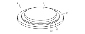
- FIG. 1 is a conceptual perspective view showing an example of a laminate 1 of the present invention.
- the laminate 1 includes a glass substrate 10 and a processed substrate 11.
- the glass substrate 10 is adhered to the processed substrate 11 in order to prevent dimensional changes of the processed substrate 11, particularly warpage deformation.
- a peeling layer 12 and an adhesive layer 13 are disposed between the glass substrate 10 and the processed substrate 11.
- the release layer 12 is in contact with the glass substrate 10, and the adhesive layer 13 is in contact with the processed substrate 11.
- the laminate 1 is laminated in the order of a glass substrate 10, a release layer 12, an adhesive layer 13, and a processed substrate 11.
- the shape of the glass substrate 10 is determined according to the processed substrate 11, in FIG. 1, the shape of the glass substrate 10 and the processed substrate 11 is a substantially disc shape.
- the release layer 12 for example, a resin that decomposes when irradiated with a laser can be used. A substance that efficiently absorbs laser light and converts it into heat can also be added to the resin. For example, carbon black, graphite powder, fine metal powder, dye, pigment and the like.
- the release layer 12 is formed by plasma CVD, spin coating by a sol-gel method, or the like.
- the adhesive layer 13 is made of a resin, and is applied and formed by, for example, various printing methods, inkjet methods, spin coating methods, roll coating methods, and the like.
- An ultraviolet curable tape can also be used. After the glass substrate 10 is peeled from the processed substrate 11 by the release layer 12, the adhesive layer 13 is dissolved and removed with a solvent or the like.
- the ultraviolet curable tape can be removed with a peeling tape after being irradiated with ultraviolet rays.
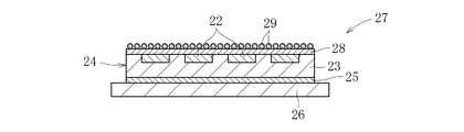
- FIGS. 2A to 2G are conceptual cross-sectional views showing a manufacturing process of a fan-out type WLP.
- FIG. 2A shows a state in which the adhesive layer 21 is formed on one surface of the support member 20. A peeling layer may be formed between the support member 20 and the adhesive layer 21 as necessary.
- FIG. 2B a plurality of semiconductor chips 22 are pasted on the adhesive layer 21. At that time, the surface on the active side of the semiconductor chip 22 is brought into contact with the adhesive layer 21.
- the semiconductor chip 22 is molded with a resin sealing material 23.
- the sealing material 23 is made of a material having little dimensional change after compression molding and little dimensional change when forming a wiring.
- the processed substrate 24 on which the semiconductor chip 22 is molded is separated from the support member 20, and then bonded and fixed to the glass substrate 26 through the adhesive layer 25.
- the surface of the processed substrate 24 opposite to the surface on which the semiconductor chip 22 is embedded is disposed on the glass substrate 26 side.
- the laminate 27 can be obtained.
- FIG. 2F after transporting the obtained laminated body 27, as shown in FIG. 2F, after forming the wiring 28 on the surface of the processed substrate 24 on the side where the semiconductor chip 22 is embedded, a plurality of solder bumps 29 are formed. .
- the processed substrate 24 is cut for each semiconductor chip 22 and used for a subsequent packaging process (FIG. 2G).
- the obtained glass original plate was cut into a wafer shape to obtain a glass substrate, and the surface of the glass substrate was polished with a polishing apparatus to reduce the overall thickness deviation of the glass substrate.
- both surfaces of the glass substrate were sandwiched between a pair of polishing pads having different outer diameters, and both surfaces of the glass substrate were polished while rotating the glass substrate and the pair of polishing pads together.
- control was sometimes performed so that a part of the glass substrate protruded from the polishing pad.
- the polishing pad was made of urethane, the average particle size of the polishing slurry used in the polishing treatment was 2.5 ⁇ m, and the polishing rate was 15 m / min.
- a semiconductor laser having a wavelength of 349 ⁇ m (laser output: 50 mW, pulse width: several ns) is irradiated to a point with a depth of 30 ⁇ m on the glass substrate, and consists of a plurality of dots on the surface of the glass substrate by thermal shock.
- An information identification unit was formed.
- the center distance of the dots was 25 ⁇ m
- the diameter of the dots was 3 ⁇ m
- the dots were constituted by cracks extending from the inside to the surface layer.
- FIG. 3 is a photomicrograph showing the information identification unit, and the black dots in the photo are dots.
- the information identifying unit can be identified by an optical element such as a CCD camera, and no cracks connecting the dots were observed.
- the overall thickness deviation was 0.55 ⁇ m and the warpage amount was 30 ⁇ m.
- the sample Nos After preparing the glass raw material so as to have a glass composition of 1 to 7, the glass raw material is put into a glass melting furnace and melted at 1500 to 1600 ° C., and then the molten glass is supplied to an overflow down-draw molding apparatus. Each was molded to 8 mm. Next, under the same conditions as in [Example 1], the glass original plate is cut into a wafer shape, and then the surface of the obtained glass substrate is polished by a polishing apparatus, so that the overall thickness deviation of the glass substrate is reduced. Furthermore, the information identification part was formed in the glass substrate with the semiconductor laser.
- the whole board thickness deviation and the curvature amount were measured, the whole board thickness deviation was 3 micrometers each, and the curvature amount was 70 micrometers, respectively, but after forming an information identification part
- the overall thickness deviation was 0.45 ⁇ m and the warpage amount was 35 ⁇ m.
- the average coefficient of thermal expansion ⁇ 30 to 380 in the temperature range of 30 to 380 ° C. is a value measured with a dilatometer.
- the density ⁇ is a value measured by the well-known Archimedes method.
- strain point Ps, annealing point Ta, and softening point Ts are values measured based on the method of ASTM C336.
- the temperature at a high temperature viscosity of 10 4.0 dPa ⁇ s, 10 3.0 dPa ⁇ s, and 10 2.5 dPa ⁇ s is a value measured by a platinum ball pulling method.
- the liquid phase temperature TL is the temperature at which crystals pass after passing through a standard sieve 30 mesh (500 ⁇ m), putting the glass powder remaining on 50 mesh (300 ⁇ m) into a platinum boat and holding it in a temperature gradient furnace for 24 hours. It is the value measured by microscopic observation.
- the Young's modulus E refers to a value measured by the resonance method.
Landscapes
- Engineering & Computer Science (AREA)
- Physics & Mathematics (AREA)
- Optics & Photonics (AREA)
- Chemical & Material Sciences (AREA)
- Mechanical Engineering (AREA)
- Plasma & Fusion (AREA)
- Materials Engineering (AREA)
- Organic Chemistry (AREA)
- General Chemical & Material Sciences (AREA)
- Geochemistry & Mineralogy (AREA)
- Chemical Kinetics & Catalysis (AREA)
- Life Sciences & Earth Sciences (AREA)
- Health & Medical Sciences (AREA)
- Toxicology (AREA)
- Laser Beam Processing (AREA)
- Surface Treatment Of Glass (AREA)
- Ceramic Engineering (AREA)
- Glass Compositions (AREA)
- Laminated Bodies (AREA)
Abstract
Description

11、26 ガラス基板
12、24 加工基板
13 剥離層
14、21、25 接着層
20 支持部材
22 半導体チップ
23 封止材
28 配線
29 半田バンプ
Claims (14)
- 全体板厚偏差が2.0μm未満であり、且つ複数のドットからなる情報識別部を有することを特徴とすることを特徴とするガラス基板。
- ドットがレーザー照射によるサーマルショックで形成されてなることを特徴とする請求項1に記載のガラス基板。
- ドットが内部から表層に向かって伸びるクラックにより形成されていることを特徴とする請求項1又は2に記載のガラス基板。
- 隣り合うドットの中心間隔が100μm以下であることを特徴とする請求項1~3の何れかに記載のガラス基板。
- ドットの直径が0.5~10μmであることを特徴とする請求項1~4の何れかに記載のガラス基板。
- 情報識別部に、ガラス基板の製造会社名、ガラス基板の材質、ガラス基板の熱膨張係数、ガラス基板の外径、ガラス基板の板厚、ガラス基板の全体板厚偏差、ガラス基板の製造年月日、ガラス基板の出荷年月日、ガラス基板のシリアル番号の内、一種又は二種以上の情報が入力されていることを特徴とする請求項1~5の何れかに記載のガラス基板。
- 反り量が60μm以下であることを特徴とする請求項1~6の何れかに記載のガラス基板。
- 表面の全部又は一部が研磨面であることを特徴とする請求項1~7の何れかに記載のガラス基板。
- ガラス内部に成形合流面を有することを特徴とする請求項1~8の何れかに記載のガラス基板。
- 外形がウエハ形状であることを特徴とする請求項1~9の何れかに記載のガラス基板。
- 半導体パッケージの製造工程で加工基板の支持に用いることを特徴とする請求項1~10の何れかに記載のガラス基板。
- 少なくとも加工基板と加工基板を支持するためのガラス基板とを備える積層体であって、ガラス基板が請求項1~11の何れかに記載のガラス基板であることを特徴とする積層体。
- 加工基板が、少なくとも封止材でモールドされた半導体チップを備えることを特徴とする請求項12に記載の積層体。
- (1)ガラス原板を切断して、ガラス基板を得る工程と、(2)ガラス基板の全体板厚偏差が2.0μm未満になるように、ガラス基板の表面を研磨する工程と、(3)レーザー照射によるサーマルショックにより、ガラス基板の内部から表層に向かって伸びるクラックを形成することにより、複数のドットで構成される情報識別部を形成する工程と、を有することを特徴とするガラス基板の製造方法。
Priority Applications (4)
| Application Number | Priority Date | Filing Date | Title |
|---|---|---|---|
| CN201680004324.XA CN107112203B (zh) | 2015-02-23 | 2016-01-22 | 玻璃基板及使用其的层叠体 |
| KR1020177015487A KR102522297B1 (ko) | 2015-02-23 | 2016-01-22 | 유리 기판 및 이것을 사용한 적층체 |
| US15/552,539 US10669184B2 (en) | 2015-02-23 | 2016-01-22 | Glass substrate and laminate using same |
| JP2017501987A JPWO2016136348A1 (ja) | 2015-02-23 | 2016-01-22 | ガラス基板及びこれを用いた積層体 |
Applications Claiming Priority (2)
| Application Number | Priority Date | Filing Date | Title |
|---|---|---|---|
| JP2015032455A JP6519221B2 (ja) | 2015-02-23 | 2015-02-23 | ガラス基板及びこれを用いた積層体 |
| JP2015-032455 | 2015-02-23 |
Publications (1)
| Publication Number | Publication Date |
|---|---|
| WO2016136348A1 true WO2016136348A1 (ja) | 2016-09-01 |
Family
ID=56788413
Family Applications (1)
| Application Number | Title | Priority Date | Filing Date |
|---|---|---|---|
| PCT/JP2016/051932 Ceased WO2016136348A1 (ja) | 2015-02-23 | 2016-01-22 | ガラス基板及びこれを用いた積層体 |
Country Status (6)
| Country | Link |
|---|---|
| US (1) | US10669184B2 (ja) |
| JP (2) | JP6519221B2 (ja) |
| KR (1) | KR102522297B1 (ja) |
| CN (1) | CN107112203B (ja) |
| TW (1) | TWI671865B (ja) |
| WO (1) | WO2016136348A1 (ja) |
Cited By (7)
| Publication number | Priority date | Publication date | Assignee | Title |
|---|---|---|---|---|
| WO2019044148A1 (ja) * | 2017-08-31 | 2019-03-07 | 日本電気硝子株式会社 | 支持ガラス基板及びこれを用いた積層基板 |
| JP2019047106A (ja) * | 2017-08-31 | 2019-03-22 | 日本電気硝子株式会社 | 支持ガラス基板及びこれを用いた積層基板 |
| JP2020514219A (ja) * | 2016-12-22 | 2020-05-21 | ショット アクチエンゲゼルシャフトSchott AG | 薄板ガラス基板、その製造方法および製造装置 |
| CN115925234A (zh) * | 2017-08-10 | 2023-04-07 | Agc株式会社 | Tft用玻璃基板 |
| DE102018209589B4 (de) | 2017-06-22 | 2023-05-04 | Schott Ag | Verbund aus einem Bauteil, insbesondere einem elektronischen Bauteil, und einem Glas- oder Glaskeramikmaterial sowie Verfahren zu dessen Herstellung |
| WO2024085083A1 (ja) * | 2022-10-21 | 2024-04-25 | Agc株式会社 | ガラス基板 |
| JP7510839B2 (ja) | 2017-02-28 | 2024-07-04 | コーニング インコーポレイテッド | 厚み変動を抑制したガラス物品、その製造方法、及びそのための装置 |
Families Citing this family (6)
| Publication number | Priority date | Publication date | Assignee | Title |
|---|---|---|---|---|
| WO2020005555A1 (en) * | 2018-06-28 | 2020-01-02 | Corning Incorporated | Continuous methods of making glass ribbon and as-drawn glass articles from the same |
| DE102020104973A1 (de) * | 2019-03-04 | 2020-09-10 | Schott Ag | Glassubstrat für eine Fahrzeugscheibe, insbesondere für die Frontscheibe eines Fahrzeugs |
| JP7303081B2 (ja) * | 2019-09-24 | 2023-07-04 | 日本碍子株式会社 | 仮固定基板、複合基板および電子部品の剥離方法 |
| WO2022230716A1 (ja) * | 2021-04-30 | 2022-11-03 | Agc株式会社 | 導光板および導光板の製造方法 |
| US11631650B2 (en) * | 2021-06-15 | 2023-04-18 | International Business Machines Corporation | Solder transfer integrated circuit packaging |
| JP7739813B2 (ja) * | 2021-07-28 | 2025-09-17 | Agc株式会社 | ガラス基板 |
Citations (4)
| Publication number | Priority date | Publication date | Assignee | Title |
|---|---|---|---|---|
| JP2001118757A (ja) * | 1999-10-20 | 2001-04-27 | Komatsu Ltd | 微小ドットマークを有する半導体基材 |
| JP2008056508A (ja) * | 2006-08-30 | 2008-03-13 | Nippon Electric Glass Co Ltd | フラットパネルディスプレイ用ガラス基板 |
| JP2013149713A (ja) * | 2012-01-18 | 2013-08-01 | Asahi Glass Co Ltd | 電子デバイスの製造方法、およびガラス積層体の製造方法 |
| JP2014031302A (ja) * | 2012-08-06 | 2014-02-20 | Asahi Glass Co Ltd | ガラス積層体用支持基板の管理方法及び管理装置 |
Family Cites Families (9)
| Publication number | Priority date | Publication date | Assignee | Title |
|---|---|---|---|---|
| JP3694768B2 (ja) * | 1999-04-27 | 2005-09-14 | 株式会社安川電機 | レーザマーキング方法 |
| JP2003089553A (ja) * | 2001-09-13 | 2003-03-28 | Shin Etsu Chem Co Ltd | 内部マーキングされた石英ガラス、光学部材用石英ガラス基板及びマーキング方法 |
| GB0509727D0 (en) * | 2005-05-13 | 2005-06-22 | Renishaw Plc | Method and apparatus for scale manufacture |
| KR20120037950A (ko) | 2009-07-24 | 2012-04-20 | 아사히 가라스 가부시키가이샤 | 유리 부재의 품질 관리 방법 및 품질 관리 장치와 마크가 부착된 유리 부재 |
| JP5261553B2 (ja) * | 2011-09-15 | 2013-08-14 | アオイ電子株式会社 | 半導体装置およびその製造方法 |
| WO2013047190A1 (ja) | 2011-09-30 | 2013-04-04 | コニカミノルタアドバンストレイヤー株式会社 | 情報記録媒体用ガラス基板の製造方法 |
| EP2858112A4 (en) * | 2012-05-30 | 2016-04-13 | Olympus Corp | METHOD FOR PRODUCING AN IMAGING APPARATUS AND METHOD FOR PRODUCING A SEMICONDUCTOR CONSTRUCTION ELEMENT |
| TWI522324B (zh) | 2013-03-29 | 2016-02-21 | Avanstrate Inc | Glass substrate manufacturing method and glass substrate manufacturing apparatus |
| KR102145229B1 (ko) * | 2013-05-24 | 2020-08-18 | 니폰 덴키 가라스 가부시키가이샤 | 강화 유리판의 제조방법 |
-
2015
- 2015-02-23 JP JP2015032455A patent/JP6519221B2/ja active Active
-
2016
- 2016-01-22 KR KR1020177015487A patent/KR102522297B1/ko active Active
- 2016-01-22 CN CN201680004324.XA patent/CN107112203B/zh not_active Expired - Fee Related
- 2016-01-22 US US15/552,539 patent/US10669184B2/en active Active
- 2016-01-22 WO PCT/JP2016/051932 patent/WO2016136348A1/ja not_active Ceased
- 2016-01-22 JP JP2017501987A patent/JPWO2016136348A1/ja active Pending
- 2016-01-28 TW TW105102592A patent/TWI671865B/zh active
Patent Citations (4)
| Publication number | Priority date | Publication date | Assignee | Title |
|---|---|---|---|---|
| JP2001118757A (ja) * | 1999-10-20 | 2001-04-27 | Komatsu Ltd | 微小ドットマークを有する半導体基材 |
| JP2008056508A (ja) * | 2006-08-30 | 2008-03-13 | Nippon Electric Glass Co Ltd | フラットパネルディスプレイ用ガラス基板 |
| JP2013149713A (ja) * | 2012-01-18 | 2013-08-01 | Asahi Glass Co Ltd | 電子デバイスの製造方法、およびガラス積層体の製造方法 |
| JP2014031302A (ja) * | 2012-08-06 | 2014-02-20 | Asahi Glass Co Ltd | ガラス積層体用支持基板の管理方法及び管理装置 |
Cited By (15)
| Publication number | Priority date | Publication date | Assignee | Title |
|---|---|---|---|---|
| US11745459B2 (en) * | 2016-12-22 | 2023-09-05 | Schott Ag | Thin glass substrate, in particular a borosilicate glass thin glass substrate, method and apparatus for its production |
| US11890844B2 (en) | 2016-12-22 | 2024-02-06 | Schott Ag | Thin glass substrate, method and apparatus for its production |
| JP2020514219A (ja) * | 2016-12-22 | 2020-05-21 | ショット アクチエンゲゼルシャフトSchott AG | 薄板ガラス基板、その製造方法および製造装置 |
| JP2020537625A (ja) * | 2016-12-22 | 2020-12-24 | ショット アクチエンゲゼルシャフトSchott AG | 薄板ガラス基板、特にホウケイ酸ガラス薄板ガラス基板、その製造方法および製造装置 |
| JP7208141B2 (ja) | 2016-12-22 | 2023-01-18 | ショット アクチエンゲゼルシャフト | 薄板ガラス基板、その製造方法および製造装置 |
| US12005687B2 (en) | 2016-12-22 | 2024-06-11 | Schott Ag | Thin glass substrate, method and apparatus for its production |
| US11993062B2 (en) | 2016-12-22 | 2024-05-28 | Schott Ag | Composite glass pane |
| JP7315542B2 (ja) | 2016-12-22 | 2023-07-26 | ショット アクチエンゲゼルシャフト | 薄板ガラス基板、特にホウケイ酸ガラス薄板ガラス基板、その製造方法および製造装置 |
| JP7510839B2 (ja) | 2017-02-28 | 2024-07-04 | コーニング インコーポレイテッド | 厚み変動を抑制したガラス物品、その製造方法、及びそのための装置 |
| DE102018209589B4 (de) | 2017-06-22 | 2023-05-04 | Schott Ag | Verbund aus einem Bauteil, insbesondere einem elektronischen Bauteil, und einem Glas- oder Glaskeramikmaterial sowie Verfahren zu dessen Herstellung |
| CN115925234A (zh) * | 2017-08-10 | 2023-04-07 | Agc株式会社 | Tft用玻璃基板 |
| WO2019044148A1 (ja) * | 2017-08-31 | 2019-03-07 | 日本電気硝子株式会社 | 支持ガラス基板及びこれを用いた積層基板 |
| JP7276644B2 (ja) | 2017-08-31 | 2023-05-18 | 日本電気硝子株式会社 | 支持ガラス基板及びこれを用いた積層基板 |
| JP2019047106A (ja) * | 2017-08-31 | 2019-03-22 | 日本電気硝子株式会社 | 支持ガラス基板及びこれを用いた積層基板 |
| WO2024085083A1 (ja) * | 2022-10-21 | 2024-04-25 | Agc株式会社 | ガラス基板 |
Also Published As
| Publication number | Publication date |
|---|---|
| US20180339929A1 (en) | 2018-11-29 |
| JP2018029093A (ja) | 2018-02-22 |
| KR102522297B1 (ko) | 2023-04-17 |
| JP6519221B2 (ja) | 2019-05-29 |
| US10669184B2 (en) | 2020-06-02 |
| CN107112203B (zh) | 2021-08-24 |
| TW201637144A (zh) | 2016-10-16 |
| JPWO2016136348A1 (ja) | 2018-03-08 |
| CN107112203A (zh) | 2017-08-29 |
| TWI671865B (zh) | 2019-09-11 |
| KR20170120092A (ko) | 2017-10-30 |
Similar Documents
| Publication | Publication Date | Title |
|---|---|---|
| JP6519221B2 (ja) | ガラス基板及びこれを用いた積層体 | |
| JP6611079B2 (ja) | ガラス板 | |
| JP6963219B2 (ja) | 支持ガラス基板及びこれを用いた積層体 | |
| JP6742593B2 (ja) | 支持ガラス基板の製造方法及び積層体の製造方法 | |
| JP6674147B2 (ja) | 支持ガラス基板及びこれを用いた積層体 | |
| JPWO2017104513A1 (ja) | 支持ガラス基板の製造方法 | |
| JP6593676B2 (ja) | 積層体及び半導体パッケージの製造方法 | |
| JP6631935B2 (ja) | ガラス板の製造方法 | |
| TWI835738B (zh) | 支持玻璃基板、層積基板、半導體封裝之製造方法、以及玻璃基板 | |
| JP2016155736A (ja) | 支持ガラス基板及びこれを用いた積層体 | |
| TWI859074B (zh) | 支持玻璃基板、層積基板、半導體封裝之製造方法、以及玻璃基板 | |
| TWI755449B (zh) | 支撐玻璃基板及使用其的積層體、半導體封裝體及其製造方法以及電子機器 | |
| JP6813813B2 (ja) | ガラス板 | |
| JP2018095544A (ja) | 支持ガラス基板及びこれを用いた積層体 | |
| JP2019001698A (ja) | 支持ガラス基板の製造方法 | |
| WO2016098499A1 (ja) | 支持ガラス基板及びこれを用いた積層体 |
Legal Events
| Date | Code | Title | Description |
|---|---|---|---|
| 121 | Ep: the epo has been informed by wipo that ep was designated in this application |
Ref document number: 16755098 Country of ref document: EP Kind code of ref document: A1 |
|
| ENP | Entry into the national phase |
Ref document number: 2017501987 Country of ref document: JP Kind code of ref document: A |
|
| ENP | Entry into the national phase |
Ref document number: 20177015487 Country of ref document: KR Kind code of ref document: A |
|
| WWE | Wipo information: entry into national phase |
Ref document number: 15552539 Country of ref document: US |
|
| NENP | Non-entry into the national phase |
Ref country code: DE |
|
| 122 | Ep: pct application non-entry in european phase |
Ref document number: 16755098 Country of ref document: EP Kind code of ref document: A1 |