WO2016136287A1 - Cu配線の形成方法および半導体装置の製造方法 - Google Patents
Cu配線の形成方法および半導体装置の製造方法 Download PDFInfo
- Publication number
- WO2016136287A1 WO2016136287A1 PCT/JP2016/050305 JP2016050305W WO2016136287A1 WO 2016136287 A1 WO2016136287 A1 WO 2016136287A1 JP 2016050305 W JP2016050305 W JP 2016050305W WO 2016136287 A1 WO2016136287 A1 WO 2016136287A1
- Authority
- WO
- WIPO (PCT)
- Prior art keywords
- film
- forming
- wiring
- alloy
- substrate
- Prior art date
- Legal status (The legal status is an assumption and is not a legal conclusion. Google has not performed a legal analysis and makes no representation as to the accuracy of the status listed.)
- Ceased
Links
Images


Classifications
-
- H—ELECTRICITY
- H10—SEMICONDUCTOR DEVICES; ELECTRIC SOLID-STATE DEVICES NOT OTHERWISE PROVIDED FOR
- H10W—GENERIC PACKAGES, INTERCONNECTIONS, CONNECTORS OR OTHER CONSTRUCTIONAL DETAILS OF DEVICES COVERED BY CLASS H10
- H10W20/00—Interconnections in chips, wafers or substrates
- H10W20/01—Manufacture or treatment
- H10W20/031—Manufacture or treatment of conductive parts of the interconnections
- H10W20/056—Manufacture or treatment of conductive parts of the interconnections by filling conductive material into holes, grooves or trenches
- H10W20/059—Manufacture or treatment of conductive parts of the interconnections by filling conductive material into holes, grooves or trenches by reflowing or applying pressure
-
- C—CHEMISTRY; METALLURGY
- C23—COATING METALLIC MATERIAL; COATING MATERIAL WITH METALLIC MATERIAL; CHEMICAL SURFACE TREATMENT; DIFFUSION TREATMENT OF METALLIC MATERIAL; COATING BY VACUUM EVAPORATION, BY SPUTTERING, BY ION IMPLANTATION OR BY CHEMICAL VAPOUR DEPOSITION, IN GENERAL; INHIBITING CORROSION OF METALLIC MATERIAL OR INCRUSTATION IN GENERAL
- C23C—COATING METALLIC MATERIAL; COATING MATERIAL WITH METALLIC MATERIAL; SURFACE TREATMENT OF METALLIC MATERIAL BY DIFFUSION INTO THE SURFACE, BY CHEMICAL CONVERSION OR SUBSTITUTION; COATING BY VACUUM EVAPORATION, BY SPUTTERING, BY ION IMPLANTATION OR BY CHEMICAL VAPOUR DEPOSITION, IN GENERAL
- C23C14/00—Coating by vacuum evaporation, by sputtering or by ion implantation of the coating forming material
- C23C14/02—Pretreatment of the material to be coated
- C23C14/024—Deposition of sublayers, e.g. to promote adhesion of the coating
- C23C14/025—Metallic sublayers
-
- C—CHEMISTRY; METALLURGY
- C23—COATING METALLIC MATERIAL; COATING MATERIAL WITH METALLIC MATERIAL; CHEMICAL SURFACE TREATMENT; DIFFUSION TREATMENT OF METALLIC MATERIAL; COATING BY VACUUM EVAPORATION, BY SPUTTERING, BY ION IMPLANTATION OR BY CHEMICAL VAPOUR DEPOSITION, IN GENERAL; INHIBITING CORROSION OF METALLIC MATERIAL OR INCRUSTATION IN GENERAL
- C23C—COATING METALLIC MATERIAL; COATING MATERIAL WITH METALLIC MATERIAL; SURFACE TREATMENT OF METALLIC MATERIAL BY DIFFUSION INTO THE SURFACE, BY CHEMICAL CONVERSION OR SUBSTITUTION; COATING BY VACUUM EVAPORATION, BY SPUTTERING, BY ION IMPLANTATION OR BY CHEMICAL VAPOUR DEPOSITION, IN GENERAL
- C23C14/00—Coating by vacuum evaporation, by sputtering or by ion implantation of the coating forming material
- C23C14/04—Coating on selected surface areas, e.g. using masks
- C23C14/046—Coating cavities or hollow spaces, e.g. interior of tubes; Infiltration of porous substrates
-
- C—CHEMISTRY; METALLURGY
- C23—COATING METALLIC MATERIAL; COATING MATERIAL WITH METALLIC MATERIAL; CHEMICAL SURFACE TREATMENT; DIFFUSION TREATMENT OF METALLIC MATERIAL; COATING BY VACUUM EVAPORATION, BY SPUTTERING, BY ION IMPLANTATION OR BY CHEMICAL VAPOUR DEPOSITION, IN GENERAL; INHIBITING CORROSION OF METALLIC MATERIAL OR INCRUSTATION IN GENERAL
- C23C—COATING METALLIC MATERIAL; COATING MATERIAL WITH METALLIC MATERIAL; SURFACE TREATMENT OF METALLIC MATERIAL BY DIFFUSION INTO THE SURFACE, BY CHEMICAL CONVERSION OR SUBSTITUTION; COATING BY VACUUM EVAPORATION, BY SPUTTERING, BY ION IMPLANTATION OR BY CHEMICAL VAPOUR DEPOSITION, IN GENERAL
- C23C14/00—Coating by vacuum evaporation, by sputtering or by ion implantation of the coating forming material
- C23C14/06—Coating by vacuum evaporation, by sputtering or by ion implantation of the coating forming material characterised by the coating material
- C23C14/14—Metallic material, boron or silicon
- C23C14/16—Metallic material, boron or silicon on metallic substrates or on substrates of boron or silicon
- C23C14/165—Metallic material, boron or silicon on metallic substrates or on substrates of boron or silicon by cathodic sputtering
-
- C—CHEMISTRY; METALLURGY
- C23—COATING METALLIC MATERIAL; COATING MATERIAL WITH METALLIC MATERIAL; CHEMICAL SURFACE TREATMENT; DIFFUSION TREATMENT OF METALLIC MATERIAL; COATING BY VACUUM EVAPORATION, BY SPUTTERING, BY ION IMPLANTATION OR BY CHEMICAL VAPOUR DEPOSITION, IN GENERAL; INHIBITING CORROSION OF METALLIC MATERIAL OR INCRUSTATION IN GENERAL
- C23C—COATING METALLIC MATERIAL; COATING MATERIAL WITH METALLIC MATERIAL; SURFACE TREATMENT OF METALLIC MATERIAL BY DIFFUSION INTO THE SURFACE, BY CHEMICAL CONVERSION OR SUBSTITUTION; COATING BY VACUUM EVAPORATION, BY SPUTTERING, BY ION IMPLANTATION OR BY CHEMICAL VAPOUR DEPOSITION, IN GENERAL
- C23C14/00—Coating by vacuum evaporation, by sputtering or by ion implantation of the coating forming material
- C23C14/22—Coating by vacuum evaporation, by sputtering or by ion implantation of the coating forming material characterised by the process of coating
- C23C14/34—Sputtering
-
- C—CHEMISTRY; METALLURGY
- C23—COATING METALLIC MATERIAL; COATING MATERIAL WITH METALLIC MATERIAL; CHEMICAL SURFACE TREATMENT; DIFFUSION TREATMENT OF METALLIC MATERIAL; COATING BY VACUUM EVAPORATION, BY SPUTTERING, BY ION IMPLANTATION OR BY CHEMICAL VAPOUR DEPOSITION, IN GENERAL; INHIBITING CORROSION OF METALLIC MATERIAL OR INCRUSTATION IN GENERAL
- C23C—COATING METALLIC MATERIAL; COATING MATERIAL WITH METALLIC MATERIAL; SURFACE TREATMENT OF METALLIC MATERIAL BY DIFFUSION INTO THE SURFACE, BY CHEMICAL CONVERSION OR SUBSTITUTION; COATING BY VACUUM EVAPORATION, BY SPUTTERING, BY ION IMPLANTATION OR BY CHEMICAL VAPOUR DEPOSITION, IN GENERAL
- C23C14/00—Coating by vacuum evaporation, by sputtering or by ion implantation of the coating forming material
- C23C14/58—After-treatment
- C23C14/5806—Thermal treatment
-
- C—CHEMISTRY; METALLURGY
- C23—COATING METALLIC MATERIAL; COATING MATERIAL WITH METALLIC MATERIAL; CHEMICAL SURFACE TREATMENT; DIFFUSION TREATMENT OF METALLIC MATERIAL; COATING BY VACUUM EVAPORATION, BY SPUTTERING, BY ION IMPLANTATION OR BY CHEMICAL VAPOUR DEPOSITION, IN GENERAL; INHIBITING CORROSION OF METALLIC MATERIAL OR INCRUSTATION IN GENERAL
- C23C—COATING METALLIC MATERIAL; COATING MATERIAL WITH METALLIC MATERIAL; SURFACE TREATMENT OF METALLIC MATERIAL BY DIFFUSION INTO THE SURFACE, BY CHEMICAL CONVERSION OR SUBSTITUTION; COATING BY VACUUM EVAPORATION, BY SPUTTERING, BY ION IMPLANTATION OR BY CHEMICAL VAPOUR DEPOSITION, IN GENERAL
- C23C16/00—Chemical coating by decomposition of gaseous compounds, without leaving reaction products of surface material in the coating, i.e. chemical vapour deposition [CVD] processes
- C23C16/04—Coating on selected surface areas, e.g. using masks
- C23C16/045—Coating cavities or hollow spaces, e.g. interior of tubes; Infiltration of porous substrates
-
- C—CHEMISTRY; METALLURGY
- C23—COATING METALLIC MATERIAL; COATING MATERIAL WITH METALLIC MATERIAL; CHEMICAL SURFACE TREATMENT; DIFFUSION TREATMENT OF METALLIC MATERIAL; COATING BY VACUUM EVAPORATION, BY SPUTTERING, BY ION IMPLANTATION OR BY CHEMICAL VAPOUR DEPOSITION, IN GENERAL; INHIBITING CORROSION OF METALLIC MATERIAL OR INCRUSTATION IN GENERAL
- C23C—COATING METALLIC MATERIAL; COATING MATERIAL WITH METALLIC MATERIAL; SURFACE TREATMENT OF METALLIC MATERIAL BY DIFFUSION INTO THE SURFACE, BY CHEMICAL CONVERSION OR SUBSTITUTION; COATING BY VACUUM EVAPORATION, BY SPUTTERING, BY ION IMPLANTATION OR BY CHEMICAL VAPOUR DEPOSITION, IN GENERAL
- C23C16/00—Chemical coating by decomposition of gaseous compounds, without leaving reaction products of surface material in the coating, i.e. chemical vapour deposition [CVD] processes
- C23C16/06—Chemical coating by decomposition of gaseous compounds, without leaving reaction products of surface material in the coating, i.e. chemical vapour deposition [CVD] processes characterised by the deposition of metallic material
-
- C—CHEMISTRY; METALLURGY
- C23—COATING METALLIC MATERIAL; COATING MATERIAL WITH METALLIC MATERIAL; CHEMICAL SURFACE TREATMENT; DIFFUSION TREATMENT OF METALLIC MATERIAL; COATING BY VACUUM EVAPORATION, BY SPUTTERING, BY ION IMPLANTATION OR BY CHEMICAL VAPOUR DEPOSITION, IN GENERAL; INHIBITING CORROSION OF METALLIC MATERIAL OR INCRUSTATION IN GENERAL
- C23C—COATING METALLIC MATERIAL; COATING MATERIAL WITH METALLIC MATERIAL; SURFACE TREATMENT OF METALLIC MATERIAL BY DIFFUSION INTO THE SURFACE, BY CHEMICAL CONVERSION OR SUBSTITUTION; COATING BY VACUUM EVAPORATION, BY SPUTTERING, BY ION IMPLANTATION OR BY CHEMICAL VAPOUR DEPOSITION, IN GENERAL
- C23C16/00—Chemical coating by decomposition of gaseous compounds, without leaving reaction products of surface material in the coating, i.e. chemical vapour deposition [CVD] processes
- C23C16/56—After-treatment
-
- H—ELECTRICITY
- H10—SEMICONDUCTOR DEVICES; ELECTRIC SOLID-STATE DEVICES NOT OTHERWISE PROVIDED FOR
- H10D—INORGANIC ELECTRIC SEMICONDUCTOR DEVICES
- H10D64/00—Electrodes of devices having potential barriers
- H10D64/01—Manufacture or treatment
- H10D64/011—Manufacture or treatment of electrodes ohmically coupled to a semiconductor
-
- H—ELECTRICITY
- H10—SEMICONDUCTOR DEVICES; ELECTRIC SOLID-STATE DEVICES NOT OTHERWISE PROVIDED FOR
- H10P—GENERIC PROCESSES OR APPARATUS FOR THE MANUFACTURE OR TREATMENT OF DEVICES COVERED BY CLASS H10
- H10P14/00—Formation of materials, e.g. in the shape of layers or pillars
- H10P14/40—Formation of materials, e.g. in the shape of layers or pillars of conductive or resistive materials
-
- H—ELECTRICITY
- H10—SEMICONDUCTOR DEVICES; ELECTRIC SOLID-STATE DEVICES NOT OTHERWISE PROVIDED FOR
- H10P—GENERIC PROCESSES OR APPARATUS FOR THE MANUFACTURE OR TREATMENT OF DEVICES COVERED BY CLASS H10
- H10P14/00—Formation of materials, e.g. in the shape of layers or pillars
- H10P14/40—Formation of materials, e.g. in the shape of layers or pillars of conductive or resistive materials
- H10P14/42—Formation of materials, e.g. in the shape of layers or pillars of conductive or resistive materials using a gas or vapour
- H10P14/43—Chemical deposition, e.g. chemical vapour deposition [CVD]
-
- H—ELECTRICITY
- H10—SEMICONDUCTOR DEVICES; ELECTRIC SOLID-STATE DEVICES NOT OTHERWISE PROVIDED FOR
- H10P—GENERIC PROCESSES OR APPARATUS FOR THE MANUFACTURE OR TREATMENT OF DEVICES COVERED BY CLASS H10
- H10P14/00—Formation of materials, e.g. in the shape of layers or pillars
- H10P14/40—Formation of materials, e.g. in the shape of layers or pillars of conductive or resistive materials
- H10P14/42—Formation of materials, e.g. in the shape of layers or pillars of conductive or resistive materials using a gas or vapour
- H10P14/44—Physical vapour deposition [PVD]
-
- H—ELECTRICITY
- H10—SEMICONDUCTOR DEVICES; ELECTRIC SOLID-STATE DEVICES NOT OTHERWISE PROVIDED FOR
- H10P—GENERIC PROCESSES OR APPARATUS FOR THE MANUFACTURE OR TREATMENT OF DEVICES COVERED BY CLASS H10
- H10P95/00—Generic processes or apparatus for manufacture or treatments not covered by the other groups of this subclass
- H10P95/90—Thermal treatments, e.g. annealing or sintering
-
- H—ELECTRICITY
- H10—SEMICONDUCTOR DEVICES; ELECTRIC SOLID-STATE DEVICES NOT OTHERWISE PROVIDED FOR
- H10W—GENERIC PACKAGES, INTERCONNECTIONS, CONNECTORS OR OTHER CONSTRUCTIONAL DETAILS OF DEVICES COVERED BY CLASS H10
- H10W20/00—Interconnections in chips, wafers or substrates
- H10W20/01—Manufacture or treatment
-
- H—ELECTRICITY
- H10—SEMICONDUCTOR DEVICES; ELECTRIC SOLID-STATE DEVICES NOT OTHERWISE PROVIDED FOR
- H10W—GENERIC PACKAGES, INTERCONNECTIONS, CONNECTORS OR OTHER CONSTRUCTIONAL DETAILS OF DEVICES COVERED BY CLASS H10
- H10W20/00—Interconnections in chips, wafers or substrates
- H10W20/01—Manufacture or treatment
- H10W20/031—Manufacture or treatment of conductive parts of the interconnections
- H10W20/032—Manufacture or treatment of conductive parts of the interconnections of conductive barrier, adhesion or liner layers
-
- H—ELECTRICITY
- H10—SEMICONDUCTOR DEVICES; ELECTRIC SOLID-STATE DEVICES NOT OTHERWISE PROVIDED FOR
- H10W—GENERIC PACKAGES, INTERCONNECTIONS, CONNECTORS OR OTHER CONSTRUCTIONAL DETAILS OF DEVICES COVERED BY CLASS H10
- H10W20/00—Interconnections in chips, wafers or substrates
- H10W20/01—Manufacture or treatment
- H10W20/031—Manufacture or treatment of conductive parts of the interconnections
- H10W20/032—Manufacture or treatment of conductive parts of the interconnections of conductive barrier, adhesion or liner layers
- H10W20/033—Manufacture or treatment of conductive parts of the interconnections of conductive barrier, adhesion or liner layers in openings in dielectrics
-
- H—ELECTRICITY
- H10—SEMICONDUCTOR DEVICES; ELECTRIC SOLID-STATE DEVICES NOT OTHERWISE PROVIDED FOR
- H10W—GENERIC PACKAGES, INTERCONNECTIONS, CONNECTORS OR OTHER CONSTRUCTIONAL DETAILS OF DEVICES COVERED BY CLASS H10
- H10W20/00—Interconnections in chips, wafers or substrates
- H10W20/01—Manufacture or treatment
- H10W20/031—Manufacture or treatment of conductive parts of the interconnections
- H10W20/032—Manufacture or treatment of conductive parts of the interconnections of conductive barrier, adhesion or liner layers
- H10W20/042—Manufacture or treatment of conductive parts of the interconnections of conductive barrier, adhesion or liner layers the barrier, adhesion or liner layers being seed or nucleation layers
- H10W20/045—Manufacture or treatment of conductive parts of the interconnections of conductive barrier, adhesion or liner layers the barrier, adhesion or liner layers being seed or nucleation layers for deposition from the gaseous phase, e.g. for chemical vapour deposition [CVD]
-
- H—ELECTRICITY
- H10—SEMICONDUCTOR DEVICES; ELECTRIC SOLID-STATE DEVICES NOT OTHERWISE PROVIDED FOR
- H10W—GENERIC PACKAGES, INTERCONNECTIONS, CONNECTORS OR OTHER CONSTRUCTIONAL DETAILS OF DEVICES COVERED BY CLASS H10
- H10W20/00—Interconnections in chips, wafers or substrates
- H10W20/01—Manufacture or treatment
- H10W20/031—Manufacture or treatment of conductive parts of the interconnections
- H10W20/032—Manufacture or treatment of conductive parts of the interconnections of conductive barrier, adhesion or liner layers
- H10W20/055—Manufacture or treatment of conductive parts of the interconnections of conductive barrier, adhesion or liner layers by formation methods other than physical vapour deposition [PVD], chemical vapour deposition [CVD] or liquid deposition
- H10W20/0552—Manufacture or treatment of conductive parts of the interconnections of conductive barrier, adhesion or liner layers by formation methods other than physical vapour deposition [PVD], chemical vapour deposition [CVD] or liquid deposition by diffusing metallic dopants to react with dielectrics
-
- H—ELECTRICITY
- H10—SEMICONDUCTOR DEVICES; ELECTRIC SOLID-STATE DEVICES NOT OTHERWISE PROVIDED FOR
- H10W—GENERIC PACKAGES, INTERCONNECTIONS, CONNECTORS OR OTHER CONSTRUCTIONAL DETAILS OF DEVICES COVERED BY CLASS H10
- H10W20/00—Interconnections in chips, wafers or substrates
- H10W20/01—Manufacture or treatment
- H10W20/031—Manufacture or treatment of conductive parts of the interconnections
- H10W20/056—Manufacture or treatment of conductive parts of the interconnections by filling conductive material into holes, grooves or trenches
-
- H—ELECTRICITY
- H10—SEMICONDUCTOR DEVICES; ELECTRIC SOLID-STATE DEVICES NOT OTHERWISE PROVIDED FOR
- H10W—GENERIC PACKAGES, INTERCONNECTIONS, CONNECTORS OR OTHER CONSTRUCTIONAL DETAILS OF DEVICES COVERED BY CLASS H10
- H10W20/00—Interconnections in chips, wafers or substrates
- H10W20/40—Interconnections external to wafers or substrates, e.g. back-end-of-line [BEOL] metallisations or vias connecting to gate electrodes
- H10W20/41—Interconnections external to wafers or substrates, e.g. back-end-of-line [BEOL] metallisations or vias connecting to gate electrodes characterised by their conductive parts
- H10W20/425—Barrier, adhesion or liner layers
-
- H—ELECTRICITY
- H10—SEMICONDUCTOR DEVICES; ELECTRIC SOLID-STATE DEVICES NOT OTHERWISE PROVIDED FOR
- H10W—GENERIC PACKAGES, INTERCONNECTIONS, CONNECTORS OR OTHER CONSTRUCTIONAL DETAILS OF DEVICES COVERED BY CLASS H10
- H10W20/00—Interconnections in chips, wafers or substrates
- H10W20/40—Interconnections external to wafers or substrates, e.g. back-end-of-line [BEOL] metallisations or vias connecting to gate electrodes
- H10W20/41—Interconnections external to wafers or substrates, e.g. back-end-of-line [BEOL] metallisations or vias connecting to gate electrodes characterised by their conductive parts
- H10W20/435—Cross-sectional shapes or dispositions of interconnections
-
- H—ELECTRICITY
- H10—SEMICONDUCTOR DEVICES; ELECTRIC SOLID-STATE DEVICES NOT OTHERWISE PROVIDED FOR
- H10W—GENERIC PACKAGES, INTERCONNECTIONS, CONNECTORS OR OTHER CONSTRUCTIONAL DETAILS OF DEVICES COVERED BY CLASS H10
- H10W20/00—Interconnections in chips, wafers or substrates
- H10W20/40—Interconnections external to wafers or substrates, e.g. back-end-of-line [BEOL] metallisations or vias connecting to gate electrodes
- H10W20/45—Interconnections external to wafers or substrates, e.g. back-end-of-line [BEOL] metallisations or vias connecting to gate electrodes characterised by their insulating parts
- H10W20/48—Insulating materials thereof
-
- H—ELECTRICITY
- H10—SEMICONDUCTOR DEVICES; ELECTRIC SOLID-STATE DEVICES NOT OTHERWISE PROVIDED FOR
- H10W—GENERIC PACKAGES, INTERCONNECTIONS, CONNECTORS OR OTHER CONSTRUCTIONAL DETAILS OF DEVICES COVERED BY CLASS H10
- H10W20/00—Interconnections in chips, wafers or substrates
- H10W20/40—Interconnections external to wafers or substrates, e.g. back-end-of-line [BEOL] metallisations or vias connecting to gate electrodes
- H10W20/41—Interconnections external to wafers or substrates, e.g. back-end-of-line [BEOL] metallisations or vias connecting to gate electrodes characterised by their conductive parts
- H10W20/44—Conductive materials thereof
- H10W20/4403—Conductive materials thereof based on metals, e.g. alloys, metal silicides
- H10W20/4421—Conductive materials thereof based on metals, e.g. alloys, metal silicides the principal metal being copper
Definitions
- the present invention relates to a Cu wiring formation method and a semiconductor device manufacturing method in which Cu or Cu alloy is buried in trenches and vias formed in a substrate to form Cu wiring.
- a wafer In the manufacture of semiconductor devices, various processes such as film formation and etching are repeatedly performed on a semiconductor wafer (hereinafter simply referred to as a wafer) to manufacture a desired device. In response to demands for finer and higher integration of wiring patterns, it is required to reduce wiring resistance (improve conductivity) and improve electromigration resistance.
- the entire surface of an interlayer insulating film having trenches and vias formed on a wafer is made of tantalum metal (Ta), titanium (Ti), tantalum nitride (TaN), titanium nitride (TiN), or the like.
- a barrier film is formed by physical vapor deposition (PVD) plasma sputtering, a Cu seed film is also formed on the barrier film by plasma sputtering, and Cu plating is applied thereon to completely embed trenches and holes.
- PVD physical vapor deposition
- a technique has been proposed in which excess copper thin film and barrier film on the wafer surface are removed by polishing treatment by CMP (Chemical Mechanical Polishing) (for example, Patent Document 1).
- a Ru film having good wettability with Cu is formed on a barrier film made of Ta or TaN by chemical vapor deposition (CVD) with essentially good step coverage.
- CVD chemical vapor deposition
- a wet layer composed of a barrier film and Ru or the like is formed on the entire surface of the interlayer insulating film in which concave portions such as vias and trenches are formed by chemical vapor deposition (CVD), and then a Cu film is formed by PVD.
- CVD chemical vapor deposition
- a technique has also been proposed in which the semiconductor wafer is heated to reflow Cu on the surface and bury Cu in the recess (for example, Patent Document 4).
- Patent Document 3 can embed Cu in a fine trench and form a low-resistance Cu wiring, a trench and a via are formed using this technique.
- Cu forms grains at the bottom of the trench, which may hinder Cu filling in the via.
- Patent Document 4 is effective for a fine trench, a single wafer may contain various width trenches, and for a wide trench. ineffective.
- the present invention provides a Cu wiring forming method capable of forming a Cu wiring having a low resistance by embedding Cu or a Cu alloy with good burying efficiency and efficiency into trenches and vias formed in a substrate, and A method for manufacturing a semiconductor device is provided.
- a Cu or Cu alloy is formed in the trench and the via with respect to the substrate having a trench having a predetermined pattern and a film having a via formed at the bottom of the trench on the surface.
- Forming a Cu wiring by embedding copper, forming a barrier film on the surface of the film, and then a wet layer made of a metal material on which Cu or a Cu alloy is wetted on the surface of the barrier film.
- the Cu-based seed film is poured into the via to fill the via, and then the Cu-based Cu or Cu alloy is formed on the substrate surface after the via is filled.
- the said formed by PVD flowable condition on the wetting layer, the method of forming the Cu wiring and a embedding the Cu-based layer in the trench is provided.
- a trench having a predetermined pattern is formed, and the trench and the substrate on which an interlayer insulating film having a via connecting the bottom of the trench and a lower layer wiring is formed.
- a semiconductor device manufacturing method for manufacturing a semiconductor device by forming Cu wiring by burying Cu or a Cu alloy in a via, and forming a barrier film on a surface of the interlayer insulating film; Forming a wetted layer made of a metal material to which Cu or a Cu alloy is wetted, forming a Cu-based seed film made of Cu or a Cu alloy on the surface of the wetted layer by PVD, and then Heating the substrate after forming the system seed film, pouring the Cu system seed film into the via to fill the via, and then filling the via A Cu-based film made of Cu or a Cu alloy is formed on the surface of the plate by PVD under conditions that allow flow on the wetted layer, and the Cu-based film is embedded in the trench, and then the entire surface is polished.
- a storage medium that operates on a computer and stores a program for controlling a Cu wiring forming system, the program being executed according to the first aspect described above.
- a storage medium is provided that causes a computer to control the Cu wiring formation system so that a Cu wiring formation method is performed.
- a Cu-based seed film is formed and heated to cause the Cu-based seed film to flow and to form Cu or Cu alloy in a fine via. Can be easily embedded.
- a Cu-based film is formed by PVD under conditions that allow flow on a wetted layer having good wettability to Cu or Cu alloy. Since it is buried in the trench, good embedding can be obtained without causing inconvenience such as obstruction of embedding in the via. Further, since Cu or Cu alloy is embedded by PVD in this way, impurities can be reduced as compared with plating, and the resistance of the Cu wiring can be further reduced. Also, since only the vias are embedded by flowing the Cu-based seed film by heating, it is not necessary to perform an inefficient process as in the case of performing reflow in a wide trench, and the efficiency is high.
- high-temperature ionized PVD is preferable.
- the crystal size of Cu or Cu alloy can be increased, and the resistance of the Cu wiring can be further reduced.
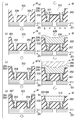
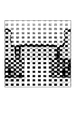
- FIG. 1 It is a flowchart which shows the formation method of Cu wiring which concerns on one Embodiment of this invention. It is process sectional drawing for demonstrating the formation method of Cu wiring which concerns on one Embodiment of this invention. It is a TEM photograph which shows the cross-sectional state after forming a Cu seed film
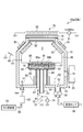
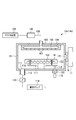
- FIG. 6 is a cross-sectional view showing a Cu-based film forming apparatus for forming a Cu-based film mounted in the film forming system of FIG. 5.
- FIG. 6 is a cross-sectional view showing a liner film forming apparatus for forming a liner film mounted on the film forming system of FIG. 5.
- Cu wiring is formed by burying Cu or a Cu alloy together in the trench and via.
- an interlayer insulating film 202 made of a SiO 2 film, a low dielectric constant (Low-k) film (SiCO, SiCOH, etc.), etc. is formed on a lower structure 201 (details are omitted) including a lower layer wiring 211, and an interlayer insulating film is formed.
- a wafer W having a trench 203 and a via 204 formed in a predetermined pattern on the film 202 is prepared (step 1, FIG. 2A).
- the via 204 is formed from the bottom of the trench 203 to the lower layer wiring 211.
- Such a wafer W is preferably removed of moisture on the insulating film surface and residues during etching / ashing by a Degas process or a Pre-Clean process.
- a barrier film 205 that suppresses the diffusion of Cu is formed on the entire surface including the surfaces of the trench 203 and the via 204 (step 2, FIG. 2B).
- the barrier film 205 preferably has a high barrier property against Cu and has a low resistance, and a Ti film, a TiN film, a Ta film, a TaN film, a Ta / TaN two-layer film, or a Mn film is preferably used. be able to.
- a TaCN film, W film, WN film, WCN film, Zr film, ZrN film, V film, VN film, Nb film, NbN film, or the like can also be used.
- the barrier film can be formed by, for example, ionized PVD (Ionized Physical Vapor Deposition; iPVD) formed while attracting ions to the wafer. Moreover, it can also form into a film by other PVDs, such as normal sputtering and ion plating, and can also form into a film by CVD and ALD (Atomic Layer Deposition). CVD or ALD may use plasma.
- the barrier film is preferably formed thin, and preferably 1 to 10 nm. Since the Mn film reacts with Si in the interlayer insulating film 202 to form a silicate and the barrier film 205 can be formed on the interlayer insulating film 202 side as a self-aligned barrier film, the volume of Cu in the Cu wiring is increased. The effect of reducing the resistance of the Cu wiring is high. For this reason, a Mn film is preferable from the viewpoint of reducing the resistance of the Cu wiring.
- the Mn film is preferably formed by CVD or ALD.
- a film forming method for forming a Mn film by CVD and ALD those described in JP-A-2014-135465 can be used.
- a liner film 206 as a wetted layer for ensuring wettability to Cu or Cu alloy is formed on the barrier film 205 (step 3, FIG. 2C).
- a Ru film or a Co film having particularly good wettability with respect to Cu can be preferably used.
- the liner film 206 which is a wetted layer has good wettability with respect to Cu or Cu alloy, as will be described later, the Cu-based film is embedded when the Cu-based film is reflowed and by PVD. In this case, good fluidity (mobility) of Cu or Cu alloy can be ensured.
- the liner film 206 is preferably formed as thin as 1 to 5 nm, for example, from the viewpoint of reducing the resistance of the wiring by increasing the volume of Cu to be embedded.
- the liner film 206 is preferably formed by CVD. Thereby, it becomes possible to form a film with a thinner film thickness with good step coverage.
- a Ru film is used as the liner film 206, it is preferable to form a film by thermal CVD using, for example, ruthenium carbonyl (Ru 3 (CO) 12 ) as a film forming material.
- film forming materials other than ruthenium carbonyl such as (cyclopentadienyl) (2,4-dimethylpentadienyl) ruthenium, bis (cyclopentadienyl) (2,4-methylpentadienyl) ruthenium, (2 , 4-dimethylpentadienyl) (ethylcyclopentadienyl) ruthenium, ruthenium pentadienyl compounds such as bis (2,4-methylpentadienyl) (ethylcyclopentadienyl) ruthenium can also be used.
- atomic layer deposition ALD
- it can also form into a film by PVD.
- a Co film when a Co film is used, it can be formed by CVD, ALD, or PVD.
- a Cu-based seed film 207 made of Cu or a Cu alloy is formed on the surface of the liner film 206 by PVD (step 4, FIG. 2 (d)).
- the Cu-based seed film 207 is for securing Cu or Cu alloy embedded in the via 204 by the next reflow process. Therefore, the film thickness of the Cu-based seed film 207 may be a film thickness corresponding to a small amount for embedding the via 204. For example, a thickness of about 1 to 40 nm is sufficient. Further, since the via 204 may be buried by reflow, the Cu-based seed film 207 does not need to be a continuous film.
- Cu-based seed film 207 when a Cu alloy is used as the Cu-based seed film 207, typical examples include Cu—Al and Cu—Mn. As other Cu alloys, Cu—Mg, Cu—Ag, Cu—Sn, Cu—Pb, Cu—Zn, Cu—Pt, Cu—Au, Cu—Ni, Cu—Co, Cu—Ti, etc. are used. be able to.
- the Cu-based seed film 207 only needs to be formed on the inner walls of the trench 203 and the via 204, and it is not necessary to consider an overhang or the like. If the trench 203 is closed, the next reflow process cannot be performed, so the film thickness and coverage must be such that the trench 203 or the via 204 does not close. From this point, the film is formed while attracting ions to the wafer. iPVD is preferred.
- the wafer W is heated and reflow processing is performed (step 5, FIG. 2 (e)).
- a Cu-based seed film 207 made of Cu or Cu alloy is poured into the via 204, and the via 204 is embedded.
- the heating temperature for the reflow treatment is preferably in the range of 200 to 400 ° C.
- the temperature is lower than 200 ° C.
- the Cu-based seed film 207 hardly flows, and when the temperature is higher than 400 ° C., Cu or Cu alloy constituting the Cu-based seed film 207 is likely to aggregate, and an interlayer insulation composed of an underlying Low-k film or the like.
- the film 202 may be adversely affected. Note that if the trench filling is insufficient by performing the formation of the Cu-based film in step 4 and the reflow process in step 5 once, step 4 and step 5 may be repeated a plurality of times.
- a wafer is placed on a stage in the chamber, and an inert gas such as Ar gas, N 2 gas, or H 2 gas is evacuated into the chamber, and the chamber is evacuated to a predetermined vacuum atmosphere. This can be performed by heating and heating the wafer with a resistance heater embedded in the stage.
- an inert gas such as Ar gas, N 2 gas, or H 2 gas
- a Cu-based film 208 made of Cu or Cu alloy is formed on the surface of the liner film 206 having good wettability to Cu or Cu alloy by PVD under a condition that allows flow on the liner film 206.
- the system film 208 is embedded in the trench 203 (step 6, FIG. 2 (f)).
- iPVD it is preferable to use iPVD that can ensure the fluidity of Cu or Cu alloy on the liner film 206 relatively easily.
- a high temperature process (65 to 350 ° C., preferably 230 to 300 ° C.) in which Cu migrates is suitable from the viewpoint of obtaining good embedding by providing Cu fluidity. Further, by performing PVD film formation by a high-temperature process in this way, Cu crystal grains can be grown, and the resistance of Cu wiring can be lowered.
- the pressure (process pressure) in the processing container when forming the Cu-based film 208 is preferably 1 to 100 mTorr (0.133 to 13.3 Pa), and 35 to 90 mTorr (4.66 to 12.0 Pa). More preferred.
- Cu-based film 207 When a Cu alloy is used as the Cu-based film 207, typical examples include Cu—Al and Cu—Mn. As other Cu alloys, Cu—Mg, Cu—Ag, Cu—Sn, Cu—Pb, Cu—Zn, Cu—Pt, Cu—Au, Cu—Ni, Cu—Co, Cu—Ti, etc. are used. be able to.
- an additional layer 209 made of Cu or Cu alloy is formed on the Cu-based film 208 in preparation for the subsequent planarization process as necessary (see FIG. Step 7, FIG. 2 (g)).
- the stacked layer 209 can be formed by depositing a Cu-based film by PVD such as iPVD following the Cu-based film 208. Moreover, you may form by giving Cu plating.
- the stacked layer 209, the Cu-based film 208, the liner film 206, and the barrier film 205 on the surface of the wafer W are removed and planarized by CMP (Chemical Mechanical Polishing) (step 8, FIG. 2 (h)). Thereby, the Cu wiring 210 is formed.
- CMP Chemical Mechanical Polishing
- the Cu-based seed film 207 is formed and heated to perform a reflow process.
- Cu or Cu alloy can be easily embedded in the fine via 204 by flowing the Cu-based seed film 207.
- PVD under a condition that allows flow on the liner film 206 having good wettability to Cu or Cu alloy, preferably Cu by high temperature iPVD. Since the system film 208 is formed and the Cu system film 208 is embedded in the trench 203, good embeddability can be obtained without causing inconvenience such as embedding in the via 204.
- Cu or Cu alloy is embedded by PVD in this way, impurities can be reduced as compared with plating, and the resistance of the Cu wiring can be further reduced. Further, by forming a film with high-temperature iPVD, the crystal size of Cu or Cu alloy can be increased, and the resistance of the Cu wiring can be further reduced. Since only the via 204 is embedded by reflow, it is not necessary to perform an inefficient process as in the case of performing reflow in a wide trench, which is highly efficient. That is, by appropriately combining reflow treatment and PVD filling (dry fill), Cu or Cu alloy is efficiently buried in the trench 203 and the via 204 with good filling properties to form a low resistance Cu wiring. can do.
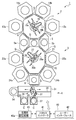
- FIG. 5 is a schematic diagram showing an example of such a film forming system.
- the film formation system 1 includes a first processing unit 2 for barrier film formation and liner film formation, a second processing unit 3 for Cu film formation, and a carry-in / out unit 4.
- a first processing unit 2 for barrier film formation and liner film formation for barrier film formation and liner film formation
- a second processing unit 3 for Cu film formation for Cu film formation
- a carry-in / out unit 4 the process from the formation of the barrier film to the formation of the additional layer is performed on the wafer W on which the trenches and vias having a predetermined pattern are formed.
- the first processing unit 2 includes a first vacuum transfer chamber 11, two barrier film forming apparatuses 12 a and 12 b connected to the wall of the first vacuum transfer chamber 11, and two liner film formations.
- the barrier film forming apparatus 12a and the liner film forming apparatus 14a, and the barrier film forming apparatus 12b and the liner film forming apparatus 14b are arranged in line-symmetric positions.
- Degas chambers 5a and 5b for degassing the wafer W are connected to other walls of the first vacuum transfer chamber 11. Further, the wafer W is transferred between the first vacuum transfer chamber 11 and a second vacuum transfer chamber 21 described later on the wall portion between the degas chambers 5a and 5b of the first vacuum transfer chamber 11. A delivery chamber 5 is connected.
- the barrier film forming apparatuses 12a and 12b, the liner film forming apparatuses 14a and 14b, the degas chambers 5a and 5b, and the delivery chamber 5 are connected to the respective sides of the first vacuum transfer chamber 11 through gate valves G. These are communicated / blocked to / from the first vacuum transfer chamber 11 by opening / closing the corresponding gate valve G.
- the inside of the first vacuum transfer chamber 11 is maintained in a predetermined vacuum atmosphere, and a first transfer mechanism 16 for transferring the wafer W is provided therein.
- the first transfer mechanism 16 is disposed substantially at the center of the first vacuum transfer chamber 11, and supports a rotating / extending / contracting portion 17 that can rotate and extend and a wafer W provided at the tip thereof. And two support arms 18a and 18b.
- the first transfer mechanism 16 carries the wafer W into and out of the barrier film forming apparatuses 12a and 12b, the liner film forming apparatuses 14a and 14b, the degas chambers 5a and 5b, and the delivery chamber 5.
- the second processing unit 3 includes a second vacuum transfer chamber 21 and two Cu-based film deposition apparatuses 22 a and 22 b configured as iPVD apparatuses connected to the wall of the second vacuum transfer chamber 21. And two Cu-based seed film deposition devices 24a and 24b configured as iPVD devices.
- the Cu-based film deposition apparatus 22a and the Cu-based seed film deposition apparatus 24a, and the Cu-based film deposition apparatus 22b and the Cu-based seed film deposition apparatus 24b are arranged in line-symmetric positions.
- the degas chambers 5a and 5b are connected to the wall portions corresponding to the two sides of the second vacuum transfer chamber 21 on the first processing unit 2 side, respectively, and the wall portion between the degas chambers 5a and 5b is connected to the walls.
- the delivery chamber 5 is connected. That is, the delivery chamber 5 and the degas chambers 5 a and 5 b are both provided between the first vacuum transfer chamber 11 and the second vacuum transfer chamber 21, and the degas chambers 5 a and 5 b are arranged on both sides of the transfer chamber 5.
- a load lock chamber 6 capable of atmospheric transfer and vacuum transfer is connected to the wall portion of the second vacuum transfer chamber 21 on the loading / unloading unit 4 side.
- the Cu-based film deposition apparatuses 22 a and 22 b, the Cu-based seed film deposition apparatuses 24 a and 24 b, the degas chambers 5 a and 5 b, and the load lock chamber 6 include a gate valve G on each wall portion of the second vacuum transfer chamber 21. These are connected to the second vacuum transfer chamber 21 by opening the corresponding gate valve, and are disconnected from the second vacuum transfer chamber 21 by closing the corresponding gate valve G.
- the delivery chamber 5 is connected to the second transfer chamber 21 without a gate valve.
- the inside of the second vacuum transfer chamber 21 is maintained in a predetermined vacuum atmosphere, which includes Cu-based film deposition devices 22a and 22b, Cu-based seed film deposition devices 24a and 24b, and degass.
- a second transfer mechanism 26 for carrying the wafer W in and out of the chambers 5a and 5b, the load lock chamber 6 and the transfer chamber 5 is provided.
- the second transfer mechanism 26 is disposed substantially at the center of the second vacuum transfer chamber 21, and has a rotation / extension / contraction part 27 that can rotate and extend / contract, and a wafer is attached to the tip of the rotation / extension / contraction part 27.
- Two support arms 28a and 28b for supporting W are provided, and these two support arms 28a and 28b are attached to the rotating / extending / contracting portion 27 so as to face opposite directions.
- the loading / unloading unit 4 is provided on the opposite side of the second processing unit 3 with the load lock chamber 6 interposed therebetween, and has an atmospheric transfer chamber 31 to which the load lock chamber 6 is connected.
- a filter (not shown) for forming a downflow of clean air is provided in the upper part of the atmospheric transfer chamber 31.
- a gate valve G is provided on the wall portion between the load lock chamber 6 and the atmospheric transfer chamber 31.
- Two connection ports 32 and 33 for connecting a carrier C that accommodates a wafer W as a substrate to be processed are provided on the wall portion of the atmospheric transfer chamber 31 that faces the wall portion to which the load lock chamber 6 is connected.
- An alignment chamber 34 for aligning the wafer W is provided on the side surface of the atmospheric transfer chamber 31.
- an atmospheric transfer transfer mechanism 36 that loads and unloads the wafer W with respect to the carrier C and loads and unloads the wafer W with respect to the load lock chamber 6 is provided.
- This atmospheric transfer mechanism 36 has two articulated arms, and can run on the rail 38 along the arrangement direction of the carrier C. The wafer W is placed on the hand 37 at each tip. It is loaded and transported.
- the Cu-based film forming apparatuses 22a and 22b can heat the wafer W, and can be used as a heating apparatus in the reflow process.
- the degas chambers 5a and 5b may be used as the heating apparatus, or a separate heating apparatus may be provided.
- the film forming system 1 has a control unit 40 for controlling each component of the film forming system 1.
- the control unit 40 includes a process controller 41 composed of a microprocessor (computer) that executes control of each component, a keyboard on which an operator inputs commands to manage the film forming system 1, and a film forming system. 1, a user interface 42 including a display for visualizing and displaying the operation status of 1, a control program for realizing processing executed by the film forming system 1 under the control of the process controller 41, various data, and processing conditions And a storage unit 43 that stores a program for causing each component of the processing apparatus to execute processing, that is, a processing recipe. Note that the user interface 42 and the storage unit 43 are connected to the process controller 41.
- the processing recipe is stored in the storage medium 43 a in the storage unit 43.
- the storage medium may be a hard disk or a portable medium such as a CDROM, DVD, or flash memory. Moreover, you may make it transmit a recipe suitably from another apparatus via a dedicated line, for example. Then, if desired, an arbitrary recipe is called from the storage unit 43 by an instruction from the user interface 42 and is executed by the process controller 41, so that a desired value in the film forming system 1 is controlled under the process controller 41. Is performed.
- a wafer W having a predetermined pattern of trenches and vias is taken out from the carrier C by the atmospheric transfer mechanism 36 and transferred to the load lock chamber 6, and the load lock chamber is transferred to the second vacuum. After the pressure is reduced to the same degree as the transfer chamber 21, the wafer W in the load lock chamber is transferred to the degas chamber 5a or 5b through the second vacuum transfer chamber 21 by the second transfer mechanism 26. Perform degassing.
- the wafer W in the degas chamber is taken out by the first transfer mechanism 16 and is carried into the barrier film forming apparatus 12a or 12b through the first vacuum transfer chamber 11 to form a barrier film.
- the wafer W is taken out from the barrier film forming apparatus 12a or 12b by the first transport mechanism 16 and loaded into the liner film forming apparatus 14a or 14b, and a Ru film, for example, is formed as the liner film.
- the wafer W is taken out from the liner film forming apparatus 14 a or 14 b by the first transfer mechanism 16 and transferred to the delivery chamber 5. Thereafter, the wafer W is taken out by the second transfer mechanism 26 and is loaded into the Cu-based seed film forming apparatus 24a or 24b via the second vacuum transfer chamber 21, and a Cu-based seed film is formed by iPVD. Note that when forming the Cu-based seed film, it is not necessary to consider the embeddability, so that the film is formed without heating the wafer W.
- the wafer W is taken out by the second transfer mechanism 26, loaded into the Cu-based film deposition apparatus 22a or 22b, the wafer W is heated, a reflow process is performed, and the Cu-based seed film is poured into the via. Perform embedding.
- a Cu-based film is formed on the wafer W by high-temperature iPVD using a Cu-based film deposition apparatus that has performed the reflow process, and Cu or a Cu alloy is embedded in the trench.
- a stacked layer is formed on the Cu-based film.
- the stacked layer can be formed by continuously forming a Cu alloy film in the same Cu-based film deposition apparatus 22a or 22b.
- the additional layer may be formed by the Cu-based seed film forming apparatus 24a or 24b.
- the wafer W is transferred to the load lock chamber 6, and the load lock chamber is returned to atmospheric pressure. Then, the wafer W on which the Cu film is formed is taken out by the atmospheric transfer mechanism 36, and is transferred to the carrier C. return. Such a process is repeated for the number of wafers W in the carrier.
- the wafer W after the additional layer is formed is transferred to a CMP apparatus and subjected to a CMP process to form a Cu wiring.
- the barrier film, the liner film, the Cu-based seed film are formed, the reflow process, the Cu-based film, and the additional layer are formed in vacuum without opening to the atmosphere. Oxidation can be suppressed as much as possible, and a high-performance Cu wiring can be obtained.
- the additional layer can also be formed by Cu plating.
- the wafer W is unloaded from the film forming system 1 and subjected to Cu plating by a plating apparatus, followed by a CMP apparatus.
- the CMP process is performed at.
- the formation of the Cu-based seed film does not require heating of the wafer W, and the Cu-based film is formed by heating the wafer W.
- the Cu-based seed film forming apparatuses 24a and 24b And the Cu-based film forming apparatuses 22a and 22b are separate apparatuses, but the temperature may be changed by using the same apparatus. In that case, the Cu-based seed film can be formed, the reflow process, and the Cu-based film can be formed using the same apparatus.
- FIG. 6 is a cross-sectional view showing an example of a Cu-based film forming apparatus.
- ICP Inductively Coupled Plasma
- the Cu-based film deposition apparatus 22a has a metal processing container 51 formed in a cylindrical shape.
- the processing vessel 51 is grounded, and an exhaust port 53 is provided at the bottom 52, and an exhaust pipe 54 is connected to the exhaust port 53.
- a throttle valve 55 and a vacuum pump 56 for adjusting pressure are connected to the exhaust pipe 54 so that the inside of the processing container 51 can be evacuated.
- a gas inlet 57 for introducing a predetermined gas into the processing container 51 is provided at the bottom 52 of the processing container 51.
- a gas supply pipe 58 is connected to the gas introduction port 57.
- the gas supply pipe 58 is connected with a rare gas such as Ar gas or other necessary gas such as N 2 gas as a plasma generation (excitation) gas. Is connected to a gas supply source 59.
- the gas supply pipe 58 is provided with a gas control unit 60 including a gas flow rate controller and a valve.
- a mounting mechanism 62 for the wafer W is provided in the processing container 51.
- the mounting mechanism 62 includes a conductive mounting base 63 formed in a disk shape and a hollow cylindrical column support 64 that supports the mounting base 63.
- the mounting table 63 is grounded via a column 64.
- a cooling jacket 65 and a resistance heater 87 provided thereon are embedded in the mounting table 63.
- the mounting table 63 is provided with a thermocouple (not shown), and the wafer temperature is controlled by the cooling jacket 65 and the resistance heater 87 based on the temperature detected by the thermocouple.
- a thin disc-like electrostatic chuck 66 configured by embedding an electrode 66b in a dielectric member 66a so that the wafer W can be attracted and held by electrostatic force. It has become. Further, the lower portion of the support column 64 extends downward through an insertion hole 67 formed at the center of the bottom 52 of the processing vessel 51. The support
- An expandable / contractible metal bellows 68 is provided so as to surround the support column 64.
- the metal bellows 68 has an upper end airtightly joined to the lower surface of the mounting table 63, and a lower end that is an upper surface of the bottom 52 of the processing vessel 51.
- the mounting mechanism 62 is allowed to move up and down while maintaining the airtightness in the processing container 51.
- three support pins 69 are vertically provided on the bottom portion 52, and pin insertion holes 70 are formed in the mounting table 63 so as to correspond to the support pins 69. Is formed. Therefore, when the mounting table 63 is lowered, the wafer W is received by the upper end portion of the support pin 69 penetrating the pin insertion hole 70, and between the transfer arm (not shown) that enters the wafer W from the outside. Can be transferred.
- a carry-in / out entrance 71 is provided for allowing the transfer arm to enter, and the carry-out / inlet 71 is provided with a gate valve G that can be opened and closed.
- a chuck power source 73 is connected to the electrode 66b of the electrostatic chuck 66 via a power supply line 72. By applying a DC voltage from the chuck power source 73 to the electrode 66b, the wafer W is attracted by electrostatic force. Retained.
- a high frequency power source 74 for bias is connected to the power supply line 72, and high frequency power for bias is supplied to the electrode 66 b of the electrostatic chuck 66 through the power supply line 72, and a high frequency bias is applied to the wafer W. Is done.
- the frequency of the high frequency bias is preferably 400 kHz to 60 MHz, for example, 13.56 MHz.
- a high-frequency transmission plate 76 made of a dielectric is airtightly provided on the ceiling of the processing vessel 51 via a seal member 77.
- a plasma generation source 78 for generating a plasma by converting a rare gas, for example, Ar gas, as a plasma excitation gas into plasma in the processing space S in the processing vessel 51 is provided above the transmission plate 76.
- the plasma generation source 78 has an induction coil 80 provided corresponding to the transmission plate 76, and a high frequency power source 81 of 13.56 MHz, for example, for plasma generation is connected to the induction coil 80. By supplying high frequency power to the induction coil 80, an induction electric field is formed in the processing space S through the transmission plate 76.
- a metal baffle plate 82 for diffusing the introduced high-frequency power is provided immediately below the transmission plate 76.
- a target 83 made of Cu or a Cu alloy having a truncated conical shell shape is provided at the lower part of the baffle plate 82 so as to surround the upper side of the processing space S, and this target 83 attracts Ar ions.
- a variable voltage DC power supply 84 for applying the DC power is connected. This power source may be an AC power source.
- a magnet 85 for applying a magnetic field to the target 83 is provided on the outer peripheral side of the target 83.
- the target 83 is sputtered by Ar ions in the plasma as Cu metal atoms or metal atomic groups, and is largely ionized when passing through the plasma.
- a cylindrical protective cover member 86 is provided below the target 83 so as to surround the processing space S.
- the protective cover member 86 is grounded, and its inner end is provided so as to surround the outer peripheral side of the mounting table 63.
- the wafer W is loaded into the processing container 51, placed on the mounting table 63, and adsorbed by the electrostatic chuck 66.
- the mounting table 63 is temperature-controlled by the cooling jacket 65 or the resistance heater 87 based on the temperature detected by a thermocouple (not shown).
- the throttle valve 55 is operated while flowing the Ar gas at a predetermined flow rate by operating the gas control unit 60 in the processing vessel 51 that has been brought to a high vacuum state of 1 ⁇ 10 ⁇ 7 Torr or less by operating the vacuum pump 56.
- the inside of the processing container 51 is controlled to maintain a predetermined degree of vacuum.
- DC power is applied from the variable DC power source 84 to the target 83, and further, high frequency power (plasma power) is supplied from the high frequency power source 81 of the plasma generation source 78 to the induction coil 80.
- a predetermined high frequency power for bias is supplied from the high frequency power source 74 for bias to the electrode 66 b of the electrostatic chuck 66.
- Ar plasma is formed by the high-frequency power supplied to the induction coil 80, and Ar ions therein are attracted to the DC voltage applied to the target 83 and collide with the target 83 and sputtered. Particles are released. At this time, the amount of particles emitted is optimally controlled by the DC voltage applied to the target 83.
- the DC power to the target 83 is preferably 4 to 12 kW, more preferably 6 to 10 kW.
- the ionization rate at this time is controlled by the high frequency power supplied from the high frequency power supply 81.
- the ionized particles enter the region of the ion sheath having a thickness of about several millimeters formed on the wafer W surface by the high frequency power for bias applied to the electrode 66b of the electrostatic chuck 66 from the high frequency power source 74 for bias.
- the Cu-based film is formed on the wafer W by being attracted so as to accelerate toward the wafer W with strong directivity.
- the wafer temperature is set high (65 to 350 ° C.) to ensure the fluidity of Cu, and the high frequency bias applied mainly to the electrode 66 b of the electrostatic chuck 66 from the high frequency power supply 74 for bias is mainly used.
- Cu or Cu alloy is embedded with good embedment even in a trench with a narrow opening by adjusting power and adjusting Cu alloy film formation and Ar etching to improve the fluidity of Cu alloy. be able to.
- the Cu-based film deposition amount (deposition rate) is T D
- the etching amount (etching rate) by ions of gas for plasma generation is T E , 0 ⁇ T E / T D ⁇ 1
- the pressure in the processing vessel 51 is preferably 1 to 100 mTorr (0.133 to 13.3 Pa), more preferably 35 to 90 mTorr (4.66 to 12.0 Pa).
- the DC power to the target is preferably 4 to 12 kW, more preferably 6 to 10 kW.
- the Cu-based seed film deposition apparatus 24a (24b) is basically the same as the Cu-based film deposition apparatus 22a (22b) shown in FIG. 6 except that the mounting table 63 is not provided with the resistance heater 87.
- a plasma sputtering apparatus can be used.
- embedding properties do not need to be emphasized. Therefore, not only iPVD but also normal PVD such as normal sputtering and ion plating can be used.
- the barrier film forming apparatus 12a (12b) can be formed by plasma sputtering using a film forming apparatus having the same configuration as the film forming apparatus shown in FIG. Further, the present invention is not limited to plasma sputtering, and may be other PVD such as normal sputtering and ion plating, and can be formed by CVD, ALD (Atomic Layer Deposition), or CVD or ALD using plasma. . From the viewpoint of reducing impurities, PVD is preferred.
- FIG. 7 is a cross-sectional view showing an example of a liner film forming apparatus, in which a Ru film is formed as a liner film by thermal CVD.
- the liner film forming apparatus 14a (14b) has a processing container 101 formed in a cylindrical body with, for example, aluminum. Inside the processing vessel 101, a mounting table 102 made of ceramics such as AlN for mounting the wafer W is disposed, and a heater 103 is provided in the mounting table 102. The heater 103 generates heat when supplied with power from a heater power source (not shown).
- a shower head 104 for introducing a processing gas for forming a Ru film, a purge gas or the like into the processing vessel 101 in a shower shape is provided so as to face the mounting table 102.
- the shower head 104 has a gas introduction port 105 in the upper portion thereof, a gas diffusion space 106 is formed in the interior thereof, and a number of gas discharge holes 107 are formed in the bottom surface thereof.
- a gas supply pipe 108 is connected to the gas inlet 105, and a gas supply source 109 for supplying a processing gas, a purge gas, and the like for forming a Ru film is connected to the gas supply pipe 108.
- the gas supply pipe 108 is provided with a gas control unit 110 including a gas flow rate controller and a valve.
- ruthenium carbonyl Ru 3 (CO) 12
- This ruthenium carbonyl can form a Ru film by thermal decomposition.
- An exhaust port 111 is provided at the bottom of the processing vessel 101, and an exhaust pipe 112 is connected to the exhaust port 111.
- a throttle valve 113 and a vacuum pump 114 for adjusting pressure are connected to the exhaust pipe 112, and the inside of the processing vessel 101 can be evacuated.
- three wafer support pins 116 for wafer transfer are provided so as to be able to project and retract with respect to the surface of the mounting table 102, and these wafer support pins 116 are fixed to the support plate 117.
- the wafer support pins 116 are moved up and down via the support plate 117 by moving the rod 119 up and down by a drive mechanism 118 such as an air cylinder.
- Reference numeral 120 denotes a bellows.
- a wafer loading / unloading port 121 is formed on the side wall of the processing chamber 101, and the wafer W is loaded into and unloaded from the first vacuum transfer chamber 11 with the gate valve G opened.
- the gate valve G is opened and the wafer W is placed on the mounting table 102, then the gate valve G is closed, and the inside of the processing vessel 101 is evacuated by the vacuum pump 114. While the wafer W is heated to a predetermined temperature from the heater 103 via the mounting table 102 while evacuating and adjusting the inside of the processing container 101 to a predetermined pressure, the gas supply pipe 108 and the shower head 104 are connected from the gas supply source 109 to the predetermined temperature. Then, a processing gas such as ruthenium carbonyl (Ru 3 (CO) 12 ) gas is introduced into the processing container 101. As a result, the reaction of the processing gas proceeds on the wafer W, and a liner film is formed on the surface of the wafer W.
- ruthenium carbonyl Ru 3 (CO) 12
- ruthenium carbonyl for example, a ruthenium pentadienyl compound as described above can be used together with a decomposition gas such as O 2 gas.
- the liner film when a Co film is formed as the liner film, it can be formed by thermal CVD as in the case of the Ru film. Further, the liner film is not limited to CVD, and can be formed by other film forming methods such as PVD.
- the semiconductor wafer is described as an example of the substrate to be processed.
- the semiconductor wafer includes not only a typical silicon wafer but also a compound semiconductor such as GaAs, SiC, and GaN.
- the substrate to be processed is not limited to a semiconductor wafer, and it is needless to say that the present invention can be applied to a glass substrate, a ceramic substrate, and the like used for an FPD (flat panel display) such as a liquid crystal display device.
- FPD flat panel display
Landscapes
- Chemical & Material Sciences (AREA)
- Mechanical Engineering (AREA)
- Organic Chemistry (AREA)
- Chemical Kinetics & Catalysis (AREA)
- Engineering & Computer Science (AREA)
- Materials Engineering (AREA)
- Metallurgy (AREA)
- General Chemical & Material Sciences (AREA)
- Physics & Mathematics (AREA)
- Thermal Sciences (AREA)
- Internal Circuitry In Semiconductor Integrated Circuit Devices (AREA)
- Physical Vapour Deposition (AREA)
- Chemical Vapour Deposition (AREA)
- Electrodes Of Semiconductors (AREA)
- Crystallography & Structural Chemistry (AREA)
Abstract
Description
最初に、本発明のCu配線の製造方法の一実施形態について図1のフローチャートおよび図2の工程断面図を参照して説明する。本実施形態ではトレンチおよびビアに一括してCuまたはCu合金を埋め込んでCu配線を形成する。
次に、本発明の実施形態に係るCu配線の形成方法の実施に用いられる成膜システムについて説明する。図5は、そのような成膜システムの一例を示す概略図である。
<Cu系膜成膜装置>
次に、本発明において主要な工程であるCu系膜の形成に用いるCu系膜成膜装置22a,22bの好適な例について説明する。図6は、Cu系膜成膜装置の一例を示す断面図である。
まず、真空ポンプ56を動作させることにより1×10⁻⁷Torr以下の高真空状態にされた処理容器51内に、ガス制御部60を操作して所定流量でArガスを流しつつスロットルバルブ55を制御して処理容器51内を所定の真空度に維持する。その後、可変直流電源84から直流電力をターゲット83に印加し、さらにプラズマ発生源78の高周波電源81から誘導コイル80に高周波電力(プラズマ電力)を供給する。一方、バイアス用高周波電源74から静電チャック66の電極66bに対して所定のバイアス用の高周波電力を供給する。
Cu系シード膜成膜装置24a(24b)としては、載置台63に抵抗ヒーター87が設けられていない以外は、基本的に、図6に示すCu系膜成膜装置22a(22b)と同様のプラズマスパッタ装置を用いることができる。また、Cu系シード膜の成膜の際には、埋め込み性を重視する必要がないため、iPVDに限らず、通常のスパッタ、イオンプレーティング等の通常のPVDを用いることもできる。
バリア膜成膜装置12a(12b)としては、ターゲット83を使用する材料に変えるのみで図6の成膜装置と同様の構成の成膜装置を用いてプラズマスパッタにより成膜することができる。また、プラズマスパッタに限定されず、通常のスパッタ、イオンプレーティング等の他のPVDであってもよく、CVDやALD(Atomic Layer Deposition)、プラズマを用いたCVDやALDで成膜することもできる。不純物を低減する観点からはPVDが好ましい。
次に、ライナー膜を形成するためのライナー膜成膜装置14a(14b)について説明する。ライナー膜は熱CVDにより好適に形成することができる。図7は、ライナー膜成膜装置の一例を示す断面図であり、熱CVDによりライナー膜としてRu膜を形成するものである。
以上、本発明の実施形態について説明したが、本発明は上記実施形態に限定されることなく種々変形可能である。上記実施形態では、被処理基板として半導体ウエハを例にとって説明したが、半導体ウエハには典型的なシリコンウエハのみならず、GaAs、SiC、GaNなどの化合物半導体も含まれる。また、被処理基板は半導体ウエハに限定されず、液晶表示装置等のFPD(フラットパネルディスプレイ)に用いるガラス基板や、セラミック基板等にも本発明を適用することができることはもちろんである。
Claims (18)
- 所定パターンのトレンチ、および前記トレンチの底に形成されたビアを有する膜が表面に形成された基板に対し、前記トレンチおよびビアにCuまたはCu合金を埋め込んでCu配線を形成するCu配線の形成方法であって、
前記膜の表面にバリア膜を形成することと、
次いで、前記バリア膜表面にCuまたはCu合金が濡れる金属材料からなる被濡れ層を形成することと、
次いで、前記被濡れ層の表面にPVDによりCuまたはCu合金からなるCu系シード膜を形成することと、
次いで、前記Cu系シード膜を形成した後の基板を加熱して、前記Cu系シード膜を前記ビア内に流し込んで前記ビアを埋めることと、
次いで、前記ビアを埋めた後の基板表面にCuまたはCu合金からなるCu系膜を、前記被濡れ層上で流動可能な条件のPVDにより形成し、前記Cu系膜を前記トレンチ内に埋め込むことと
を有するCu配線の形成方法。 - 前記被濡れ層は、膜厚が1~5nmになるように形成される、請求項1に記載のCu配線の形成方法。
- 前記被濡れ層は、RuまたはCoで構成されている、請求項1に記載のCu配線の形成方法。
- 前記被濡れ層は、CVDにより形成される、請求項1に記載のCu配線の形成方法。
- 前記Cu系シード膜を前記ビアに流し込む際の基板の加熱温度は、200~400℃である、請求項1に記載のCu配線の形成方法。
- 前記Cu系膜は、基板を65~350℃に加熱しつつイオン化PVDにより形成される、請求項1に記載のCu配線の形成方法。
- 前記Cu系シード膜を形成した後の基板を加熱することと、前記Cu系膜を形成することとを同一の装置で行う、請求項1に記載のCu配線の形成方法。
- 前記Cu系シード膜を形成することと、前記Cu系シード膜を形成した後の基板を加熱することと、前記Cu系膜を形成することとを同一の装置で行う、請求項1に記載のCu配線の形成方法。
- 所定パターンのトレンチが形成され、かつ前記トレンチの底部と下層配線との間を接続するビアを有する層間絶縁膜が形成された基板に対し、前記トレンチおよびビアにCuまたはCu合金を埋め込んでCu配線を形成して半導体装置を製造する半導体装置の製造方法であって、
前記層間絶縁膜の表面にバリア膜を形成することと、
次いで、前記バリア膜表面にCuまたはCu合金が濡れる金属材料からなる被濡れ層を形成することと、
次いで、被濡れ層の表面にPVDによりCuまたはCu合金からなるCu系シード膜を形成することと、
次いで、前記Cu系シード膜を形成した後の基板を加熱して、前記Cu系シード膜を前記ビア内に流し込んで前記ビアを埋めることと、
次いで、前記ビアを埋めた後の基板表面にCuまたはCu合金からなるCu系膜を、前記被濡れ層上で流動可能な条件のPVDにより形成し、前記Cu系膜を前記トレンチ内に埋め込むことと、
次いで、全面を研磨して前記トレンチ以外の表面の前記Cu系膜、前記被濡れ層、および前記バリア膜を除去し、Cu配線を形成することと
を有する半導体装置の製造方法。 - 前記被濡れ層は、膜厚が1~5nmになるように形成される、請求項9に記載の半導体装置の製造方法。
- 前記被濡れ層は、RuまたはCoで構成されている、請求項9に記載の半導体装置の製造方法。
- 前記被濡れ層は、CVDにより形成される、請求項9に記載の半導体装置の製造方法。
- 前記Cu系シード膜を前記ビアに流し込む際の基板の加熱温度は、200~400℃である、請求項9に記載の半導体装置の製造方法。
- 前記Cu系膜は、基板を65~350℃に加熱しつつイオン化PVDにより形成される、請求項9に記載の半導体装置の製造方法。
- 前記Cu系シード膜を形成した後の基板を加熱することと、前記Cu系膜を形成することとを同一の装置で行う、請求項9に記載の半導体装置の製造方法。
- 前記Cu系シード膜を形成することと、前記Cu系シード膜を形成した後の基板を加熱することと、前記Cu系膜を形成することとを同一の装置で行う、請求項9に記載の半導体装置の製造方法。
- 前記トレンチに前記Cu系膜を埋め込んだ後、全面を研磨する前に、前記Cu系膜の上にCuまたはCu合金からなる積み増し層を形成することをさらに有する、請求項9に記載の半導体装置の製造方法。
- コンピュータ上で動作し、Cu配線形成システムを制御するためのプログラムが記憶された記憶媒体であって、
前記プログラムは、実行時に、
所定パターンのトレンチ、および前記トレンチの底に形成されたビアを有する膜が表面に形成された基板に対し、前記トレンチおよびビアにCuまたはCu合金を埋め込んでCu配線を形成するCu配線の形成方法であって、
前記膜の表面にバリア膜を形成することと、
次いで、前記バリア膜表面にCuまたはCu合金が濡れる金属材料からなる被濡れ層を形成することと、
次いで、前記被濡れ層の表面にPVDによりCuまたはCu合金からなるCu系シード膜を形成することと、
次いで、前記Cu系シード膜を形成した後の基板を加熱して、前記Cu系シード膜を前記ビア内に流し込んで前記ビアを埋めることと、
次いで、前記ビアを埋めた後の基板表面にCuまたはCu合金からなるCu系膜を、前記被濡れ層上で流動可能な条件のPVDにより形成し、前記Cu系膜を前記トレンチ内に埋め込むことと
を有するCu配線の形成方法
が行われるように、コンピュータに前記Cu配線形成システムを制御させる、記憶媒体。
Priority Applications (2)
| Application Number | Priority Date | Filing Date | Title |
|---|---|---|---|
| US15/553,608 US10163699B2 (en) | 2015-02-26 | 2016-01-07 | Cu wiring forming method and semiconductor device manufacturing method |
| KR1020177023498A KR102008475B1 (ko) | 2015-02-26 | 2016-01-07 | Cu 배선의 형성 방법 및 반도체 장치의 제조 방법 |
Applications Claiming Priority (2)
| Application Number | Priority Date | Filing Date | Title |
|---|---|---|---|
| JP2015036895A JP6385856B2 (ja) | 2015-02-26 | 2015-02-26 | Cu配線の形成方法および半導体装置の製造方法 |
| JP2015-036895 | 2015-02-26 |
Publications (1)
| Publication Number | Publication Date |
|---|---|
| WO2016136287A1 true WO2016136287A1 (ja) | 2016-09-01 |
Family
ID=56788253
Family Applications (1)
| Application Number | Title | Priority Date | Filing Date |
|---|---|---|---|
| PCT/JP2016/050305 Ceased WO2016136287A1 (ja) | 2015-02-26 | 2016-01-07 | Cu配線の形成方法および半導体装置の製造方法 |
Country Status (5)
| Country | Link |
|---|---|
| US (1) | US10163699B2 (ja) |
| JP (1) | JP6385856B2 (ja) |
| KR (1) | KR102008475B1 (ja) |
| TW (1) | TWI689013B (ja) |
| WO (1) | WO2016136287A1 (ja) |
Families Citing this family (8)
| Publication number | Priority date | Publication date | Assignee | Title |
|---|---|---|---|---|
| US20200369918A1 (en) | 2017-08-08 | 2020-11-26 | Hitachi Chemical Company, Ltd. | Polishing solution and polishing method |
| US10438846B2 (en) | 2017-11-28 | 2019-10-08 | Taiwan Semiconductor Manufacturing Co., Ltd. | Physical vapor deposition process for semiconductor interconnection structures |
| JP7182970B2 (ja) * | 2018-09-20 | 2022-12-05 | 東京エレクトロン株式会社 | 埋め込み方法及び処理システム |
| US11222816B2 (en) * | 2020-06-16 | 2022-01-11 | Applied Materials, Inc. | Methods and apparatus for semi-dynamic bottom up reflow |
| US11527437B2 (en) * | 2020-09-15 | 2022-12-13 | Applied Materials, Inc. | Methods and apparatus for intermixing layer for enhanced metal reflow |
| US11923244B2 (en) * | 2021-03-05 | 2024-03-05 | Applied Materials, Inc. | Subtractive metals and subtractive metal semiconductor structures |
| KR102895533B1 (ko) | 2021-12-02 | 2025-12-04 | 삼성전자주식회사 | 도전 구조체를 포함하는 반도체 장치 및 이의 제조 방법 |
| US20240047267A1 (en) * | 2022-08-05 | 2024-02-08 | Applied Materials, Inc. | Tungsten gap fill with hydrogen plasma treatment |
Citations (2)
| Publication number | Priority date | Publication date | Assignee | Title |
|---|---|---|---|---|
| JP2001516146A (ja) * | 1997-08-19 | 2001-09-25 | アプライド マテリアルズ インコーポレイテッド | デュアルダマシン金属化方法 |
| JP2012216765A (ja) * | 2011-01-27 | 2012-11-08 | Tokyo Electron Ltd | Cu配線の形成方法および成膜システム |
Family Cites Families (9)
| Publication number | Priority date | Publication date | Assignee | Title |
|---|---|---|---|---|
| JP2006148075A (ja) | 2004-10-19 | 2006-06-08 | Tokyo Electron Ltd | 成膜方法及びプラズマ成膜装置 |
| JP2009105289A (ja) | 2007-10-24 | 2009-05-14 | Tokyo Electron Ltd | Cu配線の形成方法 |
| JP5417754B2 (ja) | 2008-07-11 | 2014-02-19 | 東京エレクトロン株式会社 | 成膜方法及び処理システム |
| US8859422B2 (en) * | 2011-01-27 | 2014-10-14 | Tokyo Electron Limited | Method of forming copper wiring and method and system for forming copper film |
| JP5767570B2 (ja) | 2011-01-27 | 2015-08-19 | 東京エレクトロン株式会社 | Cu配線の形成方法およびCu膜の成膜方法、ならびに成膜システム |
| KR101357531B1 (ko) * | 2011-01-27 | 2014-01-29 | 도쿄엘렉트론가부시키가이샤 | Cu 배선의 형성 방법 및 Cu막의 성막 방법, 성막 시스템, 및 기억 매체 |
| US8497202B1 (en) * | 2012-02-21 | 2013-07-30 | International Business Machines Corporation | Interconnect structures and methods of manufacturing of interconnect structures |
| JP5969306B2 (ja) * | 2012-08-08 | 2016-08-17 | 東京エレクトロン株式会社 | Cu配線の形成方法 |
| US9425092B2 (en) * | 2013-03-15 | 2016-08-23 | Applied Materials, Inc. | Methods for producing interconnects in semiconductor devices |
-
2015
- 2015-02-26 JP JP2015036895A patent/JP6385856B2/ja active Active
-
2016
- 2016-01-07 WO PCT/JP2016/050305 patent/WO2016136287A1/ja not_active Ceased
- 2016-01-07 US US15/553,608 patent/US10163699B2/en active Active
- 2016-01-07 KR KR1020177023498A patent/KR102008475B1/ko active Active
- 2016-02-24 TW TW105105369A patent/TWI689013B/zh active
Patent Citations (2)
| Publication number | Priority date | Publication date | Assignee | Title |
|---|---|---|---|---|
| JP2001516146A (ja) * | 1997-08-19 | 2001-09-25 | アプライド マテリアルズ インコーポレイテッド | デュアルダマシン金属化方法 |
| JP2012216765A (ja) * | 2011-01-27 | 2012-11-08 | Tokyo Electron Ltd | Cu配線の形成方法および成膜システム |
Also Published As
| Publication number | Publication date |
|---|---|
| KR20170106461A (ko) | 2017-09-20 |
| TW201703148A (zh) | 2017-01-16 |
| US20180047624A1 (en) | 2018-02-15 |
| JP2016162761A (ja) | 2016-09-05 |
| KR102008475B1 (ko) | 2019-08-07 |
| JP6385856B2 (ja) | 2018-09-05 |
| TWI689013B (zh) | 2020-03-21 |
| US10163699B2 (en) | 2018-12-25 |
Similar Documents
| Publication | Publication Date | Title |
|---|---|---|
| JP6385856B2 (ja) | Cu配線の形成方法および半導体装置の製造方法 | |
| JP6257217B2 (ja) | Cu配線構造の形成方法 | |
| JP5767570B2 (ja) | Cu配線の形成方法およびCu膜の成膜方法、ならびに成膜システム | |
| JP6117588B2 (ja) | Cu配線の形成方法 | |
| JP6139298B2 (ja) | Cu配線の形成方法 | |
| WO2012133400A1 (ja) | Cu配線の形成方法 | |
| JP6268008B2 (ja) | Cu配線の製造方法 | |
| JP5969306B2 (ja) | Cu配線の形成方法 | |
| JP5788785B2 (ja) | Cu配線の形成方法および成膜システム | |
| KR101923807B1 (ko) | Cu 배선의 제조 방법 및 Cu 배선 제조 시스템 | |
| KR20180068328A (ko) | 구리 배선의 제조 방법 | |
| JP6268036B2 (ja) | Cu配線の製造方法 | |
| JP2017050304A (ja) | 半導体装置の製造方法 | |
| KR20150069537A (ko) | 반도체 장치의 제조 방법 | |
| JP2012204522A (ja) | 成膜方法およびCu配線の形成方法 | |
| WO2014010333A1 (ja) | Cu配線の形成方法およびコンピュータ読み取り可能な記憶媒体 | |
| KR101357531B1 (ko) | Cu 배선의 형성 방법 및 Cu막의 성막 방법, 성막 시스템, 및 기억 매체 |
Legal Events
| Date | Code | Title | Description |
|---|---|---|---|
| 121 | Ep: the epo has been informed by wipo that ep was designated in this application |
Ref document number: 16755037 Country of ref document: EP Kind code of ref document: A1 |
|
| ENP | Entry into the national phase |
Ref document number: 20177023498 Country of ref document: KR Kind code of ref document: A |
|
| WWE | Wipo information: entry into national phase |
Ref document number: 15553608 Country of ref document: US |
|
| NENP | Non-entry into the national phase |
Ref country code: DE |
|
| 122 | Ep: pct application non-entry in european phase |
Ref document number: 16755037 Country of ref document: EP Kind code of ref document: A1 |