WO2016121968A1 - 半導体装置 - Google Patents
半導体装置 Download PDFInfo
- Publication number
- WO2016121968A1 WO2016121968A1 PCT/JP2016/052784 JP2016052784W WO2016121968A1 WO 2016121968 A1 WO2016121968 A1 WO 2016121968A1 JP 2016052784 W JP2016052784 W JP 2016052784W WO 2016121968 A1 WO2016121968 A1 WO 2016121968A1
- Authority
- WO
- WIPO (PCT)
- Prior art keywords
- field plate
- guard ring
- semiconductor device
- electrode
- conductive
- Prior art date
- Legal status (The legal status is an assumption and is not a legal conclusion. Google has not performed a legal analysis and makes no representation as to the accuracy of the status listed.)
- Ceased
Links
Images




Classifications
-
- H—ELECTRICITY
- H10—SEMICONDUCTOR DEVICES; ELECTRIC SOLID-STATE DEVICES NOT OTHERWISE PROVIDED FOR
- H10D—INORGANIC ELECTRIC SEMICONDUCTOR DEVICES
- H10D12/00—Bipolar devices controlled by the field effect, e.g. insulated-gate bipolar transistors [IGBT]
- H10D12/411—Insulated-gate bipolar transistors [IGBT]
- H10D12/441—Vertical IGBTs
- H10D12/461—Vertical IGBTs having non-planar surfaces, e.g. having trenches, recesses or pillars in the surfaces of the emitter, base or collector regions
-
- H—ELECTRICITY
- H10—SEMICONDUCTOR DEVICES; ELECTRIC SOLID-STATE DEVICES NOT OTHERWISE PROVIDED FOR
- H10D—INORGANIC ELECTRIC SEMICONDUCTOR DEVICES
- H10D12/00—Bipolar devices controlled by the field effect, e.g. insulated-gate bipolar transistors [IGBT]
- H10D12/411—Insulated-gate bipolar transistors [IGBT]
- H10D12/441—Vertical IGBTs
-
- H—ELECTRICITY
- H10—SEMICONDUCTOR DEVICES; ELECTRIC SOLID-STATE DEVICES NOT OTHERWISE PROVIDED FOR
- H10D—INORGANIC ELECTRIC SEMICONDUCTOR DEVICES
- H10D62/00—Semiconductor bodies, or regions thereof, of devices having potential barriers
- H10D62/10—Shapes, relative sizes or dispositions of the regions of the semiconductor bodies; Shapes of the semiconductor bodies
- H10D62/102—Constructional design considerations for preventing surface leakage or controlling electric field concentration
- H10D62/103—Constructional design considerations for preventing surface leakage or controlling electric field concentration for increasing or controlling the breakdown voltage of reverse-biased devices
- H10D62/105—Constructional design considerations for preventing surface leakage or controlling electric field concentration for increasing or controlling the breakdown voltage of reverse-biased devices by having particular doping profiles, shapes or arrangements of PN junctions; by having supplementary regions, e.g. junction termination extension [JTE]
- H10D62/106—Constructional design considerations for preventing surface leakage or controlling electric field concentration for increasing or controlling the breakdown voltage of reverse-biased devices by having particular doping profiles, shapes or arrangements of PN junctions; by having supplementary regions, e.g. junction termination extension [JTE] having supplementary regions doped oppositely to or in rectifying contact with regions of the semiconductor bodies, e.g. guard rings with PN or Schottky junctions
-
- H—ELECTRICITY
- H10—SEMICONDUCTOR DEVICES; ELECTRIC SOLID-STATE DEVICES NOT OTHERWISE PROVIDED FOR
- H10D—INORGANIC ELECTRIC SEMICONDUCTOR DEVICES
- H10D62/00—Semiconductor bodies, or regions thereof, of devices having potential barriers
- H10D62/10—Shapes, relative sizes or dispositions of the regions of the semiconductor bodies; Shapes of the semiconductor bodies
- H10D62/102—Constructional design considerations for preventing surface leakage or controlling electric field concentration
- H10D62/103—Constructional design considerations for preventing surface leakage or controlling electric field concentration for increasing or controlling the breakdown voltage of reverse-biased devices
- H10D62/105—Constructional design considerations for preventing surface leakage or controlling electric field concentration for increasing or controlling the breakdown voltage of reverse-biased devices by having particular doping profiles, shapes or arrangements of PN junctions; by having supplementary regions, e.g. junction termination extension [JTE]
- H10D62/106—Constructional design considerations for preventing surface leakage or controlling electric field concentration for increasing or controlling the breakdown voltage of reverse-biased devices by having particular doping profiles, shapes or arrangements of PN junctions; by having supplementary regions, e.g. junction termination extension [JTE] having supplementary regions doped oppositely to or in rectifying contact with regions of the semiconductor bodies, e.g. guard rings with PN or Schottky junctions
- H10D62/107—Buried supplementary regions, e.g. buried guard rings
-
- H—ELECTRICITY
- H10—SEMICONDUCTOR DEVICES; ELECTRIC SOLID-STATE DEVICES NOT OTHERWISE PROVIDED FOR
- H10D—INORGANIC ELECTRIC SEMICONDUCTOR DEVICES
- H10D62/00—Semiconductor bodies, or regions thereof, of devices having potential barriers
- H10D62/10—Shapes, relative sizes or dispositions of the regions of the semiconductor bodies; Shapes of the semiconductor bodies
- H10D62/124—Shapes, relative sizes or dispositions of the regions of semiconductor bodies or of junctions between the regions
- H10D62/126—Top-view geometrical layouts of the regions or the junctions
- H10D62/127—Top-view geometrical layouts of the regions or the junctions of cellular field-effect devices, e.g. multicellular DMOS transistors or IGBTs
-
- H—ELECTRICITY
- H10—SEMICONDUCTOR DEVICES; ELECTRIC SOLID-STATE DEVICES NOT OTHERWISE PROVIDED FOR
- H10D—INORGANIC ELECTRIC SEMICONDUCTOR DEVICES
- H10D62/00—Semiconductor bodies, or regions thereof, of devices having potential barriers
- H10D62/10—Shapes, relative sizes or dispositions of the regions of the semiconductor bodies; Shapes of the semiconductor bodies
- H10D62/17—Semiconductor regions connected to electrodes not carrying current to be rectified, amplified or switched, e.g. channel regions
- H10D62/393—Body regions of DMOS transistors or IGBTs
-
- H—ELECTRICITY
- H10—SEMICONDUCTOR DEVICES; ELECTRIC SOLID-STATE DEVICES NOT OTHERWISE PROVIDED FOR
- H10D—INORGANIC ELECTRIC SEMICONDUCTOR DEVICES
- H10D64/00—Electrodes of devices having potential barriers
- H10D64/111—Field plates
- H10D64/112—Field plates comprising multiple field plate segments
Definitions
- the present invention relates to a semiconductor device.
- Patent Document 1 Japanese Patent Laid-Open No. 11-330456
- Patent Document 2 Japanese Patent Laid-Open No. 2008-193043
- a field plate having a predetermined pattern is formed by etching the metal film by wet etching or the like.
- the metal film has a large amount of side etching. For this reason, when forming a field plate having a predetermined pattern, the width of the pattern must be increased excessively according to the amount of side etching. For this reason, it is difficult to reduce the size of the pressure-resistant structure portion, which hinders downsizing of the semiconductor chip.
- the semiconductor device may include an active region and a breakdown voltage structure.
- the active region and the breakdown voltage structure may be formed on the surface side of the semiconductor substrate.
- the withstand voltage structure portion may include a guard ring, a first field plate, an electrode portion, a second field plate, and a conductive connection portion.
- the guard ring may be provided surrounding the active region on the surface side of the semiconductor substrate.
- the first field plate may be provided on the surface side of the guard ring.
- the electrode part may be provided on the surface side of the first field plate.
- the second field plate may be provided between the first field plate and the electrode part.
- the conductive connection portion may electrically connect the first field plate, the electrode portion, the second field plate, and the guard ring to each other.
- the second field plate may have a smaller side etching amount than the electrode portion.
- the second field plate may be formed of a semiconductor material.
- the electrode part may be formed of a metal material.
- the width of the second field plate may be larger than the width of the electrode portion.
- the width of the second field plate may be larger than the width of the first field plate.
- the semiconductor device may further include a first insulating film and a second insulating film.
- the first insulating film may be formed between the first field plate and the second field plate.
- the second insulating film may be formed between the second field plate and the electrode part.
- the conductive connection portion may include a first conductive portion and a second conductive portion.
- the first conductive part may penetrate the first insulating film and the second insulating film and connect the electrode part and the first field plate.
- the second conductive portion may penetrate the second insulating film and connect the electrode portion and the second field plate.
- the first conductive portion may further penetrate the third insulating film between the guard ring and the first field plate to further connect the electrode portion and the guard ring.
- the first conductive portion and the second conductive portion may be arranged along the circumferential direction of the guard ring on a plane parallel to the surface of the semiconductor substrate.
- the second field plate may include a first annular portion, a second annular portion, and a partial connection portion.
- the first annular portion may be formed to cover the radially inner end of the guard ring of the first field plate.
- the second annular portion may be formed to cover the radially outer end of the guard ring of the first field plate.
- the second annular portion may be separated from the first annular portion.
- the partial connection portion may be provided in a part of the first annular portion and the second annular portion in the circumferential direction.
- the partial connection portion may partially connect the first annular portion and the second annular portion.
- the second conductive part may connect the partial connection part and the electrode part.
- the first conductive portion may penetrate a region between the first annular portion and the second annular portion where the partial connection portion is not provided.
- the guard ring may have a plurality of straight portions and a plurality of corner portions.
- the corner portions may connect the respective straight portions.
- the first conductive part and the second conductive part may be provided at corners.
- the semiconductor device may have a first guard ring and a second guard ring on the surface side of the semiconductor substrate.
- the first guard ring may surround the active region.
- the second guard ring may surround the first guard ring.
- the first field plate, the electrode part, the second field plate, and the conductive connection part may be provided in each guard ring. Between the first guard ring and the second guard ring, the distance between the second field plates may be smaller than the distance between the first field plates.
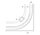
- FIG. 1 is a diagram illustrating an example of a semiconductor device 100.
- FIG. It is a figure which shows an example of the cross-section of the pressure
- FIG. 8 is a diagram illustrating an example of a positional relationship between each element illustrated in FIGS. 4 to 7 and a guard ring 22.
- FIG. 5 shows a BB ′ cross section in FIG.
- FIG. 5 shows a CC ′ cross section in FIG. 4.
- FIG. 3 is a diagram illustrating a structure example of an electrode unit 28.
- FIG. 1 is a diagram illustrating an example of the semiconductor device 100.
- FIG. 1 shows the surface structure of the semiconductor device 100.
- the semiconductor device 100 includes an active region 10 and a breakdown voltage structure 20 formed on the surface side of a semiconductor substrate such as a silicon substrate.
- the semiconductor element may be a high voltage semiconductor element such as an IGBT.
- an IGBT emitter region, a base layer functioning as a channel, a drift layer, a collector layer, and the like are sequentially formed in the active region 10 in the depth direction.
- the breakdown voltage structure 20 is provided outside the active region 10 on the substrate surface of the semiconductor device 100.
- the breakdown voltage structure 20 of this example is provided surrounding the active region 10 at the substrate end of the semiconductor device 100.
- the breakdown voltage structure 20 may be formed in a ring shape along the side of the substrate of the semiconductor device 100.
- voltage resistant structure part 20 has the some linear part 12 and the some corner
- the straight portion 12 is formed in parallel to the substrate of the semiconductor device 100.
- the corner portion 14 is formed at a corner portion of the substrate of the semiconductor device 100 and connects the adjacent linear portions 12.
- the corner 14 has a curved shape such as an arc.
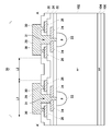
- FIG. 2 is a diagram illustrating an example of a cross-sectional structure of the pressure-resistant structure unit 20 according to the first embodiment.
- the AA ′ cross section in FIG. 1 is shown.
- the semiconductor device 100 includes a guard ring 22, a first field plate 24, a second field plate 26, an electrode portion 28, a first conductive portion 31, a second conductive portion 30, a surface side layer 102, a first layer. 1 insulating film 34, second insulating film 36, third insulating film 32, back surface side layer 104, and back surface side electrode 106.
- the surface side layer 102 functions as a drift layer of a semiconductor element such as an IGBT.
- the back side layer 104 functions as a collector layer of a semiconductor element such as an IGBT.
- the back side electrode 106 functions as a collector electrode of a semiconductor element such as an IGBT.
- the front surface side layer 102, the back surface side layer 104, and the back surface side electrode 106 are also formed to extend in the active region 10.
- a base layer of a semiconductor element such as an IGBT, an emitter region, and the like are appropriately formed on the surface side of the surface side layer 102 in the active region 10.
- a cross-sectional structure of the semiconductor device 100 is not limited to the one having the front surface side layer 102, the back surface side layer 104, and the back surface side electrode 106.
- the semiconductor device 100 has a cross-sectional structure corresponding to a semiconductor element formed in the active region 10.
- one or more guard rings 22 are formed on the surface side of the surface side layer 102.
- the guard ring 22 has a conductivity type different from that of the surface side layer 102.
- the surface side layer 102 is n-type
- the guard ring 22 is p-type.
- a depletion layer is formed between the guard ring 22 and the surface-side layer 102, and the depletion layer can be extended toward the substrate end portion of the semiconductor device 100.
- the depletion layer end (depletion layer end) on the circumferential direction (depletion layer extending direction) side of the substrate does not reach the substrate end but is separated.
- the guard ring 22 has a ring shape and is provided so as to surround the active region 10 shown in FIG. When a plurality of guard rings 22 are provided, each guard ring 22 is provided concentrically. For example, among the plurality of guard rings 22, the innermost guard ring 22 is provided surrounding the active region 10, and the next guard ring 22 is provided surrounding the innermost guard ring 22.
- the shape of the guard ring 22 on the surface of the semiconductor device 100 may be the same shape as the pressure-resistant structure portion 20 shown in FIG.
- the third insulating film 32 is formed on the surface of the surface side layer 102.
- the third insulating film 32 may be a layer obtained by oxidizing the surface side layer 102 or a layer in which a dielectric is deposited by CVD or the like, or may be an insulating film formed by another method.
- the third insulating film 32 is formed between the surface side layer 102 and the first field plate 24 and separates them.
- the first field plate 24 is provided on the surface side of the guard ring 22.
- the first field plate 24 of this example is formed in a predetermined pattern on the surface of the third insulating film 32.
- the first field plate 24 has, for example, a ring shape and is formed so as to cover the guard ring 22.
- the area of the first field plate 24 in a plane parallel to the substrate surface of the semiconductor device 100 may be larger than the area of the guard ring 22.
- the first insulating film 34 is formed on the surfaces of the first field plate 24 and the third insulating film 32.
- the first insulating film 34 is formed between the first field plate 24 and the second field plate 26 and separates them.
- the second field plate 26 is provided between the first field plate 24 and the electrode portion 28.
- the second field plate 26 of this example is formed in a predetermined pattern on the surface of the first insulating film 34.
- the second field plate 26 has, for example, a ring shape, and is formed so as to cover the first field plate 24. However, the second field plate 26 may not cover at least a part of the first field plate.
- the width L1 of the second field plate 26 in the radial direction of the guard ring 22 is larger than the width of the first field plate 24 in the direction.
- the radial direction of the guard ring 22 refers to a direction substantially perpendicular to the circumferential direction (stretching direction) of the guard ring 22, such as the direction of AA ′ shown in FIG.
- the position of the end portion (A ′ side end portion in FIG. 2) of the second field plate 26 in the radial direction is further positioned than the end portion of the first field plate 24 inside the substrate. It may be arranged inside. Further, the position of the end of the second field plate 26 outside the substrate (the A-side end in FIG.
- the second field plate 26 in the direction is further closer to the substrate of the semiconductor device 100 than the end of the first field plate 24 outside the substrate. It may be arranged outside.
- the area of the second field plate 26 in a plane parallel to the substrate surface of the semiconductor device 100 may be larger than the area of the first field plate 24.
- the interval L2 between the second field plates 26 may be narrower than the interval between the first field plates 24 between the two guard rings 22.
- the second insulating film 36 is formed on the surfaces of the second field plate 26 and the first insulating film 34.
- the second insulating film 36 is formed between the second field plate 26 and the electrode portion 28 and separates them.
- the electrode portion 28 is provided on the surface side of the first field plate 24 and the second field plate 26.
- the electrode portion 28 of this example is formed in a predetermined pattern on the surface of the second insulating film 36.
- the electrode portion 28 has, for example, a ring shape, and is formed in a part of a region facing the second field plate 26.
- the electrode portion 28 of this example covers the central region in the radial direction of the second field plate 26 and does not cover the end region.
- the width L1 of the second field plate 26 in the radial direction of the guard ring 22 is larger than the width of the electrode portion 28 in the direction.
- the position of the end portion inside the substrate of the second field plate 26 in this direction may be arranged further inside the substrate of the semiconductor device 100 than the end portion inside the substrate of the electrode portion 28.
- the position of the end portion of the second field plate 26 outside the substrate in this direction may be arranged further outside the substrate portion of the semiconductor device 100 than the end portion of the electrode portion 28 outside the substrate.
- the area of the second field plate 26 in a plane parallel to the substrate surface of the semiconductor device 100 may be larger than the area of the electrode portion 28.
- the electrode portion 28 may have a width in the radial direction of the guard ring 22 that may be larger or smaller than that of the first field plate 24.
- the first conductive portion 31 and the second conductive portion 30 function as a conductive connection portion that electrically connects the first field plate 24, the second field plate 26, and the electrode portion 28 to each other.
- the first conductive portion 31 of this example penetrates the first insulating film 34 and the second insulating film 36 and connects the electrode portion 28 and the first field plate 24.
- the first conductive portion 31 further penetrates the first field plate 24 and the third insulating film 32 and is connected to the surface of the guard ring 22.
- the spread of the depletion layer at the junction with the guard ring 22 and the surface side layer 102 can be controlled by the voltage applied to the electrode portion 28.
- An opening may be formed in the first insulating film 34 so as to expose a part of the surface of the first field plate 24.
- the first field plate 24 has an opening having a smaller diameter than the opening.
- the first conductive portion 31 may be formed along the surface and the side surface of the first field plate 24.
- the second conductive portion 30 penetrates through the second insulating film 36 and connects the electrode portion 28 and the second field plate 26.
- the form of a conductive connection part is not limited to the form shown in FIG.
- the conductive connection portion may have any form that can electrically connect the guard ring 22, the first field plate 24, the second field plate 26, and the electrode portion 28 to each other.
- the second conductive portion 30 may connect the first field plate 24 and the second field plate 26.
- the second field plate 26 has a smaller side etching amount than the electrode portion 28.
- the side etching amount refers to an amount etched in a direction parallel to the surface of the semiconductor substrate when a predetermined pattern is formed by etching the layer in the depth direction.
- the second field plate 26 is formed of a semiconductor material such as conductive polysilicon doped with a dopant such as phosphorus
- the electrode portion 28 is formed of a metal material such as aluminum doped with silicon.
- the electrode part 28 may be formed by the same process as the metal electrode formed on the surface side of the active region 10.
- the second field plate 26 may be thinner than the electrode portion 28.
- the thickness of the electrode portion 28 refers to the thickness of the portion exposed on the surface of the second insulating film 36. Thereby, the side etching amount of the second field plate 26 can be made smaller than that of the electrode portion 28.
- the second field plate 26 of this example is made of a semiconductor material and is thinner than the electrode portion 28 made of a metal material.
- the width of the second field plate 26 in this example is larger than that of the electrode portion 28. Therefore, it is possible to efficiently shield external charges and the like by the second field plate 26 and prevent the third insulating film 32 and the like from being charged with unnecessary charges.
- the second field plate 26 is formed by etching a semiconductor material such as polysilicon formed on the surface of the first insulating film 34 in a predetermined pattern.
- the second field plate 26 has a smaller side etching amount than the electrode portion 28. Therefore, when the second field plate 26 having a predetermined width L1 is formed at a predetermined interval L2 so as to function as a shield, it is not necessary to increase the pattern width in anticipation of side etching.
- the pattern interval L2 is set to be as small as possible according to the performance of the semiconductor manufacturing apparatus, for example. As described above, since the influence of the side etching amount is small in the second field plate 26, the pattern interval for forming the second field plate 26 is substantially equal to the interval L2 that the second field plate 26 should have. can do. For this reason, the pressure
- the second field plate 26 by forming the second field plate 26 with a semiconductor material, etching becomes easy, and variations in the shape of the second field plate 26 can be reduced. By reducing the variation in the shape of the second field plate 26 that protrudes to the outermost side in the pressure-resistant structure formed for each guard ring 22, the width of each pressure-resistant structure can be accurately controlled.
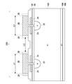
- FIG. 3 is a diagram showing a cross-sectional structure of a pressure-resistant structure 220 as a comparative example.
- the breakdown voltage structure 220 does not have the second field plate 26, and the electrode section 28 also functions as a shield.
- the electrode portion 28 is made of a metal material such as aluminum.
- the width of the electrode part 28 is set to L1 in order to function as a shield.
- the electrode portion 28 is formed by etching a metal material formed on the entire surface of the first insulating film 34 according to the pattern 29. Since the electrode portion 28 has a larger side etching amount than the second field plate 26, the width of the pattern 29 must be increased by the amount of the side etching amount. For this reason, it is difficult to reduce the size of the pressure-resistant structure 220.
- the interval between the patterns 29 is set to be as small as possible according to the performance of the semiconductor manufacturing apparatus, for example. That is, the interval between the patterns 29 is equal to the interval L2 shown in FIG. As described above, since the electrode portion 28 is side-etched, the interval between the electrode portions 28 is larger than L2.
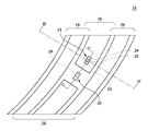
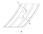
- FIG. 4 is a diagram illustrating an example of the pressure-resistant structure unit 20 according to the second embodiment.
- the first conductive portion 31 and the second conductive portion 30 are arranged along the radial direction of the guard ring 22.
- the first conductive portion 31 and the second conductive portion 30 are arranged along the circumferential direction of the guard ring 22.
- FIG. 4 shows an outline of the pressure-resistant structure 20 in the corner 14 as viewed from the surface side of the semiconductor device 100.
- the boundary lines of the stacked first field plate 24, second field plate 26, and electrode portion 28 are all shown by solid lines, but in reality, some of these boundary lines are semiconductors. It is not observed from the surface side of the device 100.
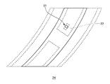
- FIG. 5 to 7 show examples of the shapes of the first field plate 24, the second field plate 26, and the electrode portion 28.
- FIG. FIG. 5 is a diagram showing the shape of the first field plate 24 by a solid line.
- the dotted line in FIG. 5 shows the other layer of the voltage withstanding structure 20 shown in FIG.
- FIG. 6 is a diagram showing the shape of the second field plate 26 by a solid line.
- FIG. 7 is a diagram showing the shape of the electrode portion 28 by a solid line.
- the first field plate 24 has an opening at the corner 14.
- the surface of the guard ring 22 is exposed through the opening.
- the first conductive portion 31 penetrates the first field plate 24.
- the width of the first field plate 24 is smaller than the width of the second field plate 26.
- the second field plate 26 has a first annular portion 38, a second annular portion 40, and a partial connection portion 42.
- the first annular portion 38 is formed to cover the radially inner end portion of the guard ring 22 of the first field plate 24.
- the second annular portion 40 is formed to cover the radially outer end of the guard ring 22 of the first field plate 24.
- the first annular portion 38 and the second annular portion 40 are formed separately from each other.
- the first annular portion 38 and the second annular portion 40 may be formed concentrically.
- the partial connection part 42 is provided in a part of the circumferential direction of the first annular part 38 and the second annular part 40, and partially connects the first annular part 38 and the second annular part 40.
- a region 41 where the partial connection portion 42 is not formed is hatched among regions sandwiched between the first annular portion 38 and the second annular portion 40. Since the second field plate 26 is not formed in the region 41, the second field plate 26 does not overlap the first field plate 24 in the region 41.
- the first conductive portion 31 is provided in the region 41.
- the second conductive part 30 connects the partial connection part 42 and the electrode part 28. That is, the rear surface side end portion of the second conductive portion 30 is connected to the partial connection portion 42 as shown in FIG.
- the first conductive portion 31 penetrates through each layer in the region where the partial connection portion 42 is not formed among the regions sandwiched between the first annular portion 38 and the second annular portion 40, and the electrode portion 28 and the guard Connect the ring 22.
- the width of the second field plate 26 may be larger than both the electrode portion 28 and the first field plate 24.
- the width of the second field plate 26 refers to the width from the end of the first annular portion 38 inside the substrate to the end of the second annular portion 40 outside the substrate.
- the widths of the first annular portion 38 and the second annular portion 40 may be the same or different.
- the first conductive portion 31 and the second conductive portion 30 are connected to the back side of the electrode portion 28.
- the first conductive part 31, the second conductive part 30, and the electrode part 28 may be integrally formed of the same material.
- the partial connection portion 42 that connects the first annular portion 38 and the second annular portion 40 is partially formed, so that the first conductive portion 31 and the second conductive portion 30 can be arranged along the circumferential direction of the guard ring 22.
- the width of the breakdown voltage structure portion 20 can be reduced compared to the case where the first conductive portion 31 and the second conductive portion 30 are arranged along the radial direction of the guard ring 22, and the semiconductor device 100 can be reduced in size. It becomes easy.
- the width of the electrode portion 28 is preferably equal to or smaller than the width obtained by subtracting the side etching amount of the electrode portion 28 from the width of the second field plate 26. Thereby, the space
- the width of the electrode portion 28 in the radial direction of the guard ring 22 may be half or less than that of the second field plate 26.
- the width of the first field plate 24 in the radial direction of the guard ring 22 may be the same as that of the second field plate 26, may be half or less, and may be 1/3 or less.
- the first field plate 24 and the second field plate 26 may have substantially the same thickness. Further, since the second field plate 26 mainly functions as a shield, the second field plate 26 may be thicker than the first field plate 24.
- the positions of the first conductive portion 31 and the second conductive portion 30 in the radial direction of the guard ring 22 are the same, but the first conductive portion 31 and the second conductive portion 30 are the same.
- the position in the radial direction may be shifted. That is, the straight line connecting the first conductive portion 31 and the second conductive portion 30 may be parallel to the circumferential direction of the guard ring 22 and may be slightly deviated from parallel.
- first conductive portion 31 and the second conductive portion 30 may be formed at each corner portion 14 of the pressure resistant structure portion 20. Further, neither the first conductive portion 31 nor the second conductive portion 30 need be formed at any corner portion 14. For example, of the four corners 14, the first conductive part 31 and the second conductive part 30 are formed in the two diagonal corners 14, and any of the conductive parts are formed in the remaining two corners 14. Not formed.
- first conductive portion 31 and the second conductive portion 30 may be formed in each corner portion 14.
- first conductive portion 31 is formed in the two diagonal corner portions 14, and the second conductive portion 30 is formed in the remaining two corner portions 14. Is done.
- first conductive portion 31 may be formed at any one of the corner portions 14, and the second conductive portion 30 may be formed at the diagonal corner portion 14. None of the conductive portions need be formed on the remaining two corner portions 14.
- FIG. 8 is a diagram showing an example of the positional relationship between each element shown in FIGS. 4 to 7 and the guard ring 22.
- the shape of the guard ring 22 is indicated by a solid line.
- the guard ring 22 has a ring shape and is provided on the back surface side of the first field plate 24.
- the guard ring 22 of this example is entirely covered with the first field plate 24.
- the guard ring 22 is electrically connected to the electrode portion 28 by the first conductive portion 31.
- the position of the end of the guard ring 22 is separated from the position of the end of the second field plate 26, but the end of the guard ring 22 and the second field plate 26 It may overlap with the end.
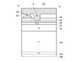
- FIG. 9 shows a BB ′ cross section in FIG.
- the breakdown voltage structure 20 has a plurality of guard rings 22 as in the example shown in FIG. 2.
- the first conductive portion 31 and the second conductive portion 30 are arranged along the circumferential direction of the guard ring 22, the radial direction B of the guard ring 22 that passes through the first conductive portion 31.
- the second conductive portion 30 does not exist.
- the other structure may be the same as the example shown in FIG.
- FIG. 10 shows a CC ′ cross section in FIG. Since the CC ′ section is a section along the circumferential direction of the guard ring 22, both the first conductive portion 31 and the second conductive portion 30 exist in the cross section.
- the second field plate 26 exists only on the C side with respect to the first conductive portion 31 and does not exist on the C ′ side. This is because the partial connection portion 42 shown in FIG. 6 exists on the C side with respect to the first conductive portion 31, whereas the partial connection portion 42 does not exist on the C ′ side. is there.
- FIG. 11 is a diagram illustrating a structure example of the electrode unit 28.
- the electrode portion 28 and the guard ring 22 are shown in the breakdown voltage structure portion 20, and the first field plate 24 and the like are omitted.
- the electrode portion 28 may be formed in an annular shape so as to surround the active region 10, or may be formed only in the corner portion 14 excluding the straight portion 12.
- the first conductive portion 31 is preferably provided at the corner portion 14.
- the electrode portion 28 may be provided on the diagonal corner portion 14 and the electrode portion 28 may not be provided on the other corner portion 14.
- a guard ring 22 having an electrode portion 28 formed in an annular shape and a guard ring 22 having an electrode portion 28 formed only in a corner portion 14 are provided. Alternatively, they may be arranged alternately. Further, in the two or more guard rings 22 in which the electrode portions 28 are provided only in the corner portions 14, the corner portions 14 in which the electrode portions 28 are provided may be different. For example, in one guard ring 22, electrode portions 28 are provided at two diagonal corner portions 14, and in the other adjacent guard ring 22, electrode portions are disposed at diagonal corner portions 14 that are orthogonal to the above diagonal. 28 may be provided.
- DESCRIPTION OF SYMBOLS 100 Semiconductor device, 10 ... Active region, 12 ... Straight part, 14 ... Corner
Landscapes
- Electrodes Of Semiconductors (AREA)
Abstract
耐圧構造部の小型化が容易な半導体装置を提供する。半導体基板の表面側に形成された活性領域および耐圧構造部を備える半導体装置であって、耐圧構造部は、半導体基板の表面側において活性領域を囲んで設けられたガードリングと、ガードリングの表面側に設けられた第1のフィールドプレートと、第1のフィールドプレートの表面側に設けられた電極部と、第1のフィールドプレートおよび電極部の間に設けられた第2のフィールドプレートと、第1のフィールドプレート、電極部、第2のフィールドプレートおよびガードリングを、互いに電気的に接続する導電接続部とを備える半導体装置を提供する。
Description
本発明は、半導体装置に関する。
従来、電界集中を緩和するフィールドプレートを、電力用半導体素子等の耐圧構造部に設けた構造が知られている(例えば特許文献1および2参照)。フィールドプレートは、例えば金属材料で形成される。
[先行技術文献]
[特許文献]
特許文献1 特開平11-330456号公報
特許文献2 特開2008-193043号公報
[先行技術文献]
[特許文献]
特許文献1 特開平11-330456号公報
特許文献2 特開2008-193043号公報
金属膜をウェットエッチング等でエッチングすることで、所定のパターンのフィールドプレートを形成する。しかし、金属膜はサイドエッチング量が大きい。このため、所定のパターンのフィールドプレートを形成する場合に、サイドエッチングされる量に応じて、パターンの幅を余計に大きくしなければならない。このため、耐圧構造部を小型化することが困難であり、半導体チップの小型化を妨げてしまう。
本発明の態様においては、半導体装置は、活性領域および耐圧構造部を備えてよい。活性領域および耐圧構造部は、半導体基板の表面側に形成されてよい。耐圧構造部は、ガードリングと、第1のフィールドプレートと、電極部と、第2のフィールドプレートと、導電接続部とを備えてよい。ガードリングは、半導体基板の表面側において活性領域を囲んで設けられてよい。第1のフィールドプレートは、ガードリングの表面側に設けられてよい。電極部は、第1のフィールドプレートの表面側に設けられてよい。第2のフィールドプレートは、第1のフィールドプレートおよび電極部の間に設けられてよい。導電接続部は、第1のフィールドプレート、電極部、第2のフィールドプレートおよびガードリングを、互いに電気的に接続してよい。第2のフィールドプレートは、電極部よりもサイドエッチング量が小さくてよい。
第2のフィールドプレートは半導体材料で形成されてよい。電極部は金属材料で形成されてよい。
ガードリングの径方向において、第2のフィールドプレートの幅は、電極部の幅よりも大きくてよい。
ガードリングの径方向において、第2のフィールドプレートの幅は、第1のフィールドプレートの幅よりも大きくてよい。
半導体装置は、第1の絶縁膜と、第2の絶縁膜とを更に備えてよい。第1の絶縁膜は、第1のフィールドプレートと第2のフィールドプレートとの間に形成されてよい。第2の絶縁膜は、第2のフィールドプレートと電極部との間に形成されてよい。導電接続部は、第1の導電部と、第2の導電部とを有してよい。第1の導電部は、第1の絶縁膜および第2の絶縁膜を貫通して、電極部と第1のフィールドプレートとを接続してよい。第2の導電部は、第2の絶縁膜を貫通して、電極部と第2のフィールドプレートとを接続してよい。
第1の導電部は、ガードリングと第1のフィールドプレートとの間の第3の絶縁膜を更に貫通して、電極部とガードリングとを更に接続してよい。
第1の導電部および第2の導電部は、半導体基板の表面と平行な面においてガードリングの周方向に沿って配列されてよい。
第2のフィールドプレートは、第1の環状部と、第2の環状部と、部分接続部とを有してよい。第1の環状部は、第1のフィールドプレートのガードリングの径方向内側の端部を覆って形成されてよい。第2の環状部は、第1のフィールドプレートのガードリングの径方向外側の端部を覆って形成されてよい。第2の環状部は、第1の環状部と分離してよい。部分接続部は、第1の環状部および第2の環状部の周方向の一部分に設けられてよい。部分接続部は、第1の環状部および第2の環状部を部分的に接続してよい。第2の導電部は、部分接続部と電極部とを接続してよい。
第1の導電部は、部分接続部が設けられていない第1の環状部および第2の環状部の間の領域を貫通してよい。
ガードリングは、複数の直線部と、複数の角部とを有してよい。角部は、それぞれの直線部を接続してよい。第1の導電部および第2の導電部は、角部に設けられてよい。
半導体装置は、半導体基板の表面側において、第1のガードリングと、第2のガードリングとを有してよい。第1のガードリングは、活性領域を囲んでよい。第2のガードリングは、第1のガードリングを囲んでよい。第1のフィールドプレート、電極部、第2のフィールドプレート、および、導電接続部は、それぞれのガードリングに設けられてよい。第1のガードリングと第2のガードリングとの間において、第1のフィールドプレートの間隔より、第2のフィールドプレートの間隔のほうが狭くてよい。
第2のフィールドプレートは半導体材料で形成されてよい。電極部は金属材料で形成されてよい。
ガードリングの径方向において、第2のフィールドプレートの幅は、電極部の幅よりも大きくてよい。
ガードリングの径方向において、第2のフィールドプレートの幅は、第1のフィールドプレートの幅よりも大きくてよい。
半導体装置は、第1の絶縁膜と、第2の絶縁膜とを更に備えてよい。第1の絶縁膜は、第1のフィールドプレートと第2のフィールドプレートとの間に形成されてよい。第2の絶縁膜は、第2のフィールドプレートと電極部との間に形成されてよい。導電接続部は、第1の導電部と、第2の導電部とを有してよい。第1の導電部は、第1の絶縁膜および第2の絶縁膜を貫通して、電極部と第1のフィールドプレートとを接続してよい。第2の導電部は、第2の絶縁膜を貫通して、電極部と第2のフィールドプレートとを接続してよい。
第1の導電部は、ガードリングと第1のフィールドプレートとの間の第3の絶縁膜を更に貫通して、電極部とガードリングとを更に接続してよい。
第1の導電部および第2の導電部は、半導体基板の表面と平行な面においてガードリングの周方向に沿って配列されてよい。
第2のフィールドプレートは、第1の環状部と、第2の環状部と、部分接続部とを有してよい。第1の環状部は、第1のフィールドプレートのガードリングの径方向内側の端部を覆って形成されてよい。第2の環状部は、第1のフィールドプレートのガードリングの径方向外側の端部を覆って形成されてよい。第2の環状部は、第1の環状部と分離してよい。部分接続部は、第1の環状部および第2の環状部の周方向の一部分に設けられてよい。部分接続部は、第1の環状部および第2の環状部を部分的に接続してよい。第2の導電部は、部分接続部と電極部とを接続してよい。
第1の導電部は、部分接続部が設けられていない第1の環状部および第2の環状部の間の領域を貫通してよい。
ガードリングは、複数の直線部と、複数の角部とを有してよい。角部は、それぞれの直線部を接続してよい。第1の導電部および第2の導電部は、角部に設けられてよい。
半導体装置は、半導体基板の表面側において、第1のガードリングと、第2のガードリングとを有してよい。第1のガードリングは、活性領域を囲んでよい。第2のガードリングは、第1のガードリングを囲んでよい。第1のフィールドプレート、電極部、第2のフィールドプレート、および、導電接続部は、それぞれのガードリングに設けられてよい。第1のガードリングと第2のガードリングとの間において、第1のフィールドプレートの間隔より、第2のフィールドプレートの間隔のほうが狭くてよい。
なお、上記の発明の概要は、本発明の特徴の全てを列挙したものではない。また、これらの特徴群のサブコンビネーションもまた、発明となりうる。
以下、発明の実施の形態を通じて本発明を説明するが、以下の実施形態は請求の範囲にかかる発明を限定するものではない。また、実施形態の中で説明されている特徴の組み合わせの全てが発明の解決手段に必須であるとは限らない。
図1は、半導体装置100の一例を示す図である。図1では、半導体装置100の表面構造を示す。半導体装置100は、シリコン基板等の半導体基板の表面側に形成された活性領域10および耐圧構造部20を備える。
活性領域10には、複数の半導体素子が形成される。半導体素子は、IGBT等の高耐圧半導体素子であってよい。例えば活性領域10には、IGBTのエミッタ領域、チャネルとして機能するベース層、ドリフト層、コレクタ層等が深さ方向に順次形成される。
耐圧構造部20は、半導体装置100の基板表面において、活性領域10よりも外側に設けられる。本例の耐圧構造部20は、半導体装置100の基板端部において、活性領域10を囲んで設けられる。耐圧構造部20は、半導体装置100の基板の辺に沿って環状に形成されてよい。例えば耐圧構造部20は、複数の直線部12と、複数の角部14とを有する。直線部12は、半導体装置100の基板に平行に形成される。角部14は、半導体装置100の基板の角部分に形成され、隣接する直線部12を接続する。角部14は、例えば円弧等の曲線形状を有する。
図2は、第1の実施形態に係る耐圧構造部20の断面構造の一例を示す図である。本例では図1におけるA-A'断面を示す。当該断面において半導体装置100は、ガードリング22、第1のフィールドプレート24、第2のフィールドプレート26、電極部28、第1の導電部31、第2の導電部30、表面側層102、第1の絶縁膜34、第2の絶縁膜36、第3の絶縁膜32、裏面側層104、および、裏面側電極106を有する。
表面側層102は、例えばIGBT等の半導体素子のドリフト層として機能する。裏面側層104は、例えばIGBT等の半導体素子のコレクタ層として機能する。裏面側電極106は、例えばIGBT等の半導体素子のコレクタ電極として機能する。表面側層102、裏面側層104および裏面側電極106は、活性領域10にも延伸して形成されている。
活性領域10における表面側層102の表面側には、例えばIGBT等の半導体素子のベース層、およびエミッタ領域等が適宜形成される。なお、半導体装置100の断面構造は、表面側層102、裏面側層104および裏面側電極106を有するものに限定されない。半導体装置100は、活性領域10に形成される半導体素子に応じた断面構造を有する。
耐圧構造部20において、表面側層102の表面側には1以上のガードリング22が形成される。ガードリング22は、表面側層102とは異なる導電型を有する。本例において表面側層102はn-型であり、ガードリング22はp型である。これにより、ガードリング22および表面側層102との間で空乏層が形成され、半導体装置100の基板端部方向へ空乏層を延伸させることができる。ただし、基板の周方向(空乏層の延伸方向)側の空乏層端部(空乏層端)は、基板端部には到達せずに離間する。
ガードリング22は環形状を有しており、図1に示した活性領域10を囲んで設けられる。ガードリング22を複数設ける場合、それぞれのガードリング22は同心状に設けられる。例えば、複数のガードリング22のうち、最内のガードリング22は活性領域10を囲んで設けられ、次のガードリング22は最内のガードリング22を囲んで設けられる。半導体装置100の表面におけるガードリング22の形状は、図1に示した耐圧構造部20と同様の形状であってよい。
第3の絶縁膜32は、表面側層102の表面に形成される。第3の絶縁膜32は、表面側層102を酸化した層、または、誘電体をCVD等により堆積させた層であってよく、他の方法で形成された絶縁膜であってもよい。第3の絶縁膜32は、表面側層102と第1のフィールドプレート24との間に形成され、これらを分離する。
第1のフィールドプレート24は、ガードリング22の表面側に設けられる。本例の第1のフィールドプレート24は、第3の絶縁膜32の表面に所定のパターンで形成される。第1のフィールドプレート24は、例えば環形状を有しており、ガードリング22を覆うように形成される。半導体装置100の基板表面と平行な面内における第1のフィールドプレート24の面積は、ガードリング22の面積よりも大きくてよい。
第1の絶縁膜34は、第1のフィールドプレート24および第3の絶縁膜32の表面に形成される。また、第1の絶縁膜34は、第1のフィールドプレート24と第2のフィールドプレート26との間に形成され、これらを分離する。
第2のフィールドプレート26は、第1のフィールドプレート24と電極部28との間に設けられる。本例の第2のフィールドプレート26は、第1の絶縁膜34の表面に所定のパターンで形成される。第2のフィールドプレート26は、例えば環形状を有しており、第1のフィールドプレート24を覆うように形成される。ただし、第2のフィールドプレート26は、第1のフィールドプレートの少なくとも一部の領域を覆わなくともよい。
例えば図2に示すように、ガードリング22の径方向における第2のフィールドプレート26の幅L1は、当該方向における第1のフィールドプレート24の幅よりも大きい。ここでガードリング22の径方向とは、例えば図1に示したA-A'の方向のように、ガードリング22の周方向(延伸方向)と略垂直な方向を指す。当該径方向における第2のフィールドプレート26の基板内側の端部(図2におけるA'側端部)の位置は、第1のフィールドプレート24の基板内側の端部よりも更に半導体装置100の基板内側に配置されてよい。また、当該方向における第2のフィールドプレート26の基板外側の端部(図2におけるA側端部)の位置は、第1のフィールドプレート24の基板外側の端部よりも更に半導体装置100の基板外側に配置されてよい。半導体装置100の基板表面と平行な面内における第2のフィールドプレート26の面積は、第1のフィールドプレート24の面積よりも大きくてよい。また、2つのガードリング22の間において、第1のフィールドプレート24の間隔より、第2のフィールドプレート26の間隔L2のほうが狭くてよい。
第2の絶縁膜36は、第2のフィールドプレート26および第1の絶縁膜34の表面に形成される。また、第2の絶縁膜36は、第2のフィールドプレート26と電極部28との間に形成され、これらを分離する。
電極部28は、第1のフィールドプレート24および第2のフィールドプレート26よりも表面側に設けられる。本例の電極部28は、第2の絶縁膜36の表面に所定のパターンで形成される。電極部28は、例えば環形状を有しており、第2のフィールドプレート26と対向する領域の一部に形成される。本例の電極部28は、第2のフィールドプレート26の径方向における中央領域を覆い、端部領域を覆わない。
図2に示すように、ガードリング22の径方向における第2のフィールドプレート26の幅L1は、当該方向における電極部28の幅よりも大きい。当該方向における第2のフィールドプレート26の基板内側の端部の位置は、電極部28の基板内側の端部よりも更に半導体装置100の基板内側に配置されてよい。また、当該方向における第2のフィールドプレート26の基板外側の端部の位置は、電極部28の基板外側の端部よりも更に半導体装置100の基板外側に配置されてよい。
半導体装置100の基板表面と平行な面内における第2のフィールドプレート26の面積は、電極部28の面積よりも大きくてよい。なお電極部28は、ガードリング22の径方向における幅が、第1のフィールドプレート24よりも大きくてよく、小さくてもよい。
第1の導電部31および第2の導電部30は、第1のフィールドプレート24、第2のフィールドプレート26および電極部28を互いに電気的に接続する導電接続部として機能する。本例の第1の導電部31は、第1の絶縁膜34および第2の絶縁膜36を貫通して、電極部28と第1のフィールドプレート24とを接続する。また、第1の導電部31は、第1のフィールドプレート24および第3の絶縁膜32を更に貫通して、ガードリング22の表面に接続される。
電極部28に印加される電圧により、ガードリング22および表面側層102との接合部分における空乏層の広がりを制御することができる。第1の絶縁膜34には、第1のフィールドプレート24の表面の一部を露出させるように開口が形成されてよい。第1のフィールドプレート24は、当該開口よりも径の小さい開口が形成される。第1の導電部31には、第1のフィールドプレート24の当該表面および側面に沿って形成されてよい。
第2の導電部30は、第2の絶縁膜36を貫通して、電極部28と第2のフィールドプレート26とを接続する。なお、導電接続部の形態は、図2に示す形態に限定されない。導電接続部は、ガードリング22、第1のフィールドプレート24、第2のフィールドプレート26および電極部28を互いに電気的に接続できる形態であればよい。他の例として、第2の導電部30が、第1のフィールドプレート24および第2のフィールドプレート26を接続してもよい。
なお、第2のフィールドプレート26は、電極部28よりもサイドエッチング量が小さい。ここでサイドエッチング量とは、当該層を深さ方向にエッチングして所定のパターンを形成した場合に、半導体基板の表面と平行な方向にエッチングされる量を指す。例えば、第2のフィールドプレート26は、リンなどのドーパントがドープされた導電性のポリシリコン等の半導体材料で形成されており、電極部28はシリコンがドープされたアルミニウム等の金属材料で形成される。電極部28は、活性領域10の表面側に形成される金属電極と同一のプロセスで形成されてよい。
また、第2のフィールドプレート26は、電極部28よりも薄くてよい。ここで電極部28の厚みは、第2の絶縁膜36の表面に露出している部分の厚みを指す。これにより、第2のフィールドプレート26のサイドエッチング量を、電極部28よりも小さくすることができる。本例の第2のフィールドプレート26は、半導体材料で形成され、且つ、金属材料の電極部28よりも薄い。
本例の第2のフィールドプレート26は、電極部28よりも幅が大きい。このため、第2のフィールドプレート26により外部電荷等を効率よくシールドして、第3の絶縁膜32等に不要な電荷がチャージされることを防ぐことができる。
また、第2のフィールドプレート26は、第1の絶縁膜34の表面に形成したポリシリコン等の半導体材料を、所定のパターンでエッチングすることで形成される。そして、第2のフィールドプレート26は、電極部28よりもサイドエッチング量が小さい。このため、シールドとして機能させるべく所定の幅L1の第2のフィールドプレート26を、所定の間隔L2で形成する場合に、サイドエッチングを見越してパターン幅を大きくしなくともよい。
パターンの間隔L2は、例えば半導体製造装置の性能に応じてできるだけ小さくなるように設定される。上述したように第2のフィールドプレート26は、サイドエッチング量の影響が小さいので、第2のフィールドプレート26を形成するためのパターン間隔を、第2のフィールドプレート26が有するべき間隔L2にほぼ等しくすることができる。このため、耐圧構造部20を小さくすることができ、半導体装置100の小型化が容易となる。
また、第2のフィールドプレート26を半導体材料で形成することでエッチングが容易になり、第2のフィールドプレート26の形状のバラツキを低減することができる。ガードリング22毎に形成される耐圧構造において最も外側に張り出している第2のフィールドプレート26の形状バラツキを低減することで、それぞれの耐圧構造の幅を精度よく制御できる。
図3は、比較例としての耐圧構造部220の断面構造を示す図である。耐圧構造部220は、第2のフィールドプレート26を有さずに、電極部28がシールドとしても機能する。電極部28はアルミニウム等の金属材料で形成される。
シールドとして機能させるべく電極部28の幅をL1にする場合を検討する。電極部28は、第1の絶縁膜34の表面全体に形成された金属材料を、パターン29に応じてエッチングすることで形成される。電極部28は、第2のフィールドプレート26よりもサイドエッチング量が大きいので、当該サイドエッチング量の分、パターン29の幅を大きくしなければならない。このため、耐圧構造部220の小型化が困難である。
また、パターン29の間隔は、例えば半導体製造装置の性能に応じてできるだけ小さくなるように設定される。つまり、パターン29の間隔は、図2に示した間隔L2と等しい。上述したように、電極部28はサイドエッチングされるので、電極部28の間隔はL2よりも大きくなる。
図4は、第2の実施形態に係る耐圧構造部20の一例を示す図である。図2に示した例では、第1の導電部31および第2の導電部30が、ガードリング22の径方向に沿って配列されている。これに対して本例では、第1の導電部31および第2の導電部30が、ガードリング22の周方向に沿って配列される。
図4では、角部14における耐圧構造部20を、半導体装置100の表面側から見た概要を示す。なお図4においては、積層されている第1のフィールドプレート24、第2のフィールドプレート26および電極部28の境界線を全て実線で示しているが、実際は、これらの境界線の一部は半導体装置100の表面側からは観察されない。
また、図5から図7において、第1のフィールドプレート24、第2のフィールドプレート26および電極部28の各形状の例を示す。図5は、第1のフィールドプレート24の形状を実線で示す図である。図5における点線は、図4に示した耐圧構造部20の他層を示している。図6は、第2のフィールドプレート26の形状を実線で示す図である。図7は、電極部28の形状を実線で示す図である。
図5に示すように、第1のフィールドプレート24は、角部14において開口を有する。当該開口により、ガードリング22の表面が露出する。当該開口により、第1の導電部31が第1のフィールドプレート24を貫通する。なお、ガードリング22の径方向において、第1のフィールドプレート24の幅は、第2のフィールドプレート26の幅よりも小さい。
図6に示すように、第2のフィールドプレート26は、第1の環状部38、第2の環状部40および部分接続部42を有する。第1の環状部38は、第1のフィールドプレート24のガードリング22の径方向内側の端部を覆って形成される。また、第2の環状部40は、第1のフィールドプレート24のガードリング22の径方向外側の端部を覆って形成される。第1の環状部38および第2の環状部40は、互いに分離して形成される。第1の環状部38および第2の環状部40は、同心状に形成されてよい。
部分接続部42は、第1の環状部38および第2の環状部40の周方向の一部分に設けられ、第1の環状部38および第2の環状部40を部分的に接続する。なお図6において、第1の環状部38および第2の環状部40で挟まれる領域のうち、部分接続部42が形成されない領域41にハッチングを付している。領域41には第2のフィールドプレート26が形成されないので、領域41では第2のフィールドプレート26が第1のフィールドプレート24に重ならない。本例では領域41に第1の導電部31が設けられる。
第2の導電部30は、部分接続部42と、電極部28とを接続する。つまり、第2の導電部30の裏面側端部は、図6に示すように部分接続部42に接続される。また、第1の導電部31は、第1の環状部38および第2の環状部40で挟まれる領域のうち、部分接続部42が形成されない領域における各層を貫通して、電極部28およびガードリング22を接続する。
第2のフィールドプレート26は、電極部28および第1のフィールドプレート24のいずれよりも幅が大きくてよい。第2のフィールドプレート26の幅とは、第1の環状部38の基板内側における端部から、第2の環状部40の基板外側における端部までの幅を指す。第1の環状部38および第2の環状部40の幅は同一であってよく、異なっていてもよい。
図7に示すように、電極部28の裏面側には、第1の導電部31および第2の導電部30が接続される。第1の導電部31、第2の導電部30および電極部28は、同一の材料で一体に形成されてよい。
上述したように、本例の第2のフィールドプレート26は、第1の環状部38および第2の環状部40を接続する部分接続部42が部分的に形成されるので、第1の導電部31および第2の導電部30をガードリング22の周方向に沿って配列させることができる。このため、第1の導電部31および第2の導電部30をガードリング22の径方向に沿って配列させる場合に比べて耐圧構造部20の幅を小さくすることができ、半導体装置100の小型化が容易となる。
電極部28の幅は、第2のフィールドプレート26の幅から、電極部28のサイドエッチング量を減じた幅以下であることが好ましい。これにより、電極部28をエッチングするときのパターンの間隔をL2以下にすることができる。また、第2のフィールドプレート26が主にシールドとして機能するので、電極部28の幅はより小さくてもよい。
一例として、ガードリング22の径方向における電極部28の幅は、第2のフィールドプレート26の半分以下であってよい。また、ガードリング22の径方向における第1のフィールドプレート24の幅は、第2のフィールドプレート26と同じであってよく、半分以下であってよく、1/3以下であってもよい。
第1のフィールドプレート24と第2のフィールドプレート26は、略同一の厚みであってよい。また、第2のフィールドプレート26が主にシールドとして機能するので、第2のフィールドプレート26は、第1のフィールドプレート24よりも厚くてもよい。
なお、図4から図7において第1の導電部31および第2の導電部30のガードリング22の径方向における位置は同一であるが、第1の導電部31および第2の導電部30の当該径方向における位置はずれていてもよい。つまり、第1の導電部31および第2の導電部30を結ぶ直線は、ガードリング22の周方向と平行であってよく、平行からわずかにずれていてもよい。
また、第1の導電部31および第2の導電部30は、耐圧構造部20のそれぞれの角部14に形成されてよい。また、いずれかの角部14には、第1の導電部31および第2の導電部30のいずれも形成されなくてよい。例えば4つの角部14のうち、対角の2つの角部14には第1の導電部31および第2の導電部30が形成され、残りの2つの角部14にはいずれの導電部も形成されない。
また、それぞれの角部14には、第1の導電部31および第2の導電部30のいずれか一方だけが形成されてもよい。例えば、4つの角部14のうち、対角の2つの角部14には第1の導電部31が形成され、残りの対角の2つの角部14には第2の導電部30が形成される。また、いずれかの角部14に第1の導電部31が形成され、対角の角部14に第2の導電部30が形成されてよい。残りの2つの角部14には、いずれの導電部も形成されなくともよい。
図8は、図4から図7に示した各要素と、ガードリング22との位置関係の一例を示す図である。図8では、ガードリング22の形状を実線で示している。上述したように、ガードリング22は環形状を有し、第1のフィールドプレート24の裏面側に設けられる。本例のガードリング22は、全体が第1のフィールドプレート24に覆われる。また、ガードリング22は、第1の導電部31により電極部28と電気的に接続される。なお図8においては、ガードリング22の端部の位置と、第2のフィールドプレート26との端部の位置とを離しているが、ガードリング22の端部と、第2のフィールドプレート26の端部とは重なっていてもよい。
図9は、図4におけるB-B'断面を示す。なお、図9においては一つのガードリング22を示すが、図2に示した例と同様に、耐圧構造部20は複数のガードリング22を有する。本例においては、第1の導電部31および第2の導電部30がガードリング22の周方向に沿って配列されているので、第1の導電部31を通るガードリング22の径方向のB-B'断面においては、第2の導電部30は存在しない。他の構造は、図2に示した例と同一であってよい。
図10は、図4におけるC-C'断面を示す。C-C'断面はガードリング22の周方向に沿った断面なので、当該断面には第1の導電部31および第2の導電部30の両方が存在する。なお、第2のフィールドプレート26が、第1の導電部31に対してC側にだけ存在し、C'側には存在しない。これは、第1の導電部31に対してC側には、図6に示した部分接続部42が存在するのに対して、C'側には部分接続部42が存在していないからである。
図11は、電極部28の構造例を示す図である。図11においては、耐圧構造部20のうち電極部28およびガードリング22のみを示しており、第1のフィールドプレート24等を省略している。それぞれのガードリング22において、電極部28は、活性領域10を囲むように環状に形成されてよいし、あるいは直線部12を除く角部14のみに形成されてもよい。いずれの構造においても、第1の導電部31は角部14に設けられることが好ましい。角部14にのみ電極部28を設ける場合、全ての角部14に電極部28を設けてよく、一部の角部14に選択的に電極部28を設けてもよい。例えば対角の角部14に電極部28を設け、他の角部14には電極部28を設けなくともよい。
また、図11に示すように、2つ以上のガードリング22において、環状に形成された電極部28を有するガードリング22と、角部14のみに形成された電極部28を有するガードリング22を、交互に配置してもよい。また、角部14にのみ電極部28を設ける2つ以上のガードリング22において、電極部28を設ける角部14を異ならせてもよい。例えば一方のガードリング22においては対角の2つの角部14に電極部28を設け、隣接する他方のガードリング22においては、上記の対角とは直交する対角の角部14に電極部28を設けてよい。
以上、本発明を実施の形態を用いて説明したが、本発明の技術的範囲は上記実施の形態に記載の範囲には限定されない。上記実施の形態に、多様な変更または改良を加えることが可能であることが当業者に明らかである。その様な変更または改良を加えた形態も本発明の技術的範囲に含まれ得ることが、請求の範囲の記載から明らかである。
請求の範囲、明細書、および図面中において示した装置、システム、プログラム、および方法における動作、手順、ステップ、および段階等の各処理の実行順序は、特段「より前に」、「先立って」等と明示しておらず、また、前の処理の出力を後の処理で用いるのでない限り、任意の順序で実現しうることに留意すべきである。請求の範囲、明細書、および図面中の動作フローに関して、便宜上「まず、」、「次に、」等を用いて説明したとしても、この順で実施することが必須であることを意味するものではない。
100・・・半導体装置、10・・・活性領域、12・・・直線部、14・・・角部、20・・・耐圧構造部、22・・・ガードリング、24・・・第1のフィールドプレート、26・・・第2のフィールドプレート、28・・・電極部、29・・・パターン、30・・・第2の導電部、31・・・第1の導電部、32・・・第3の絶縁膜、34・・・第1の絶縁膜、36・・・第2の絶縁膜、38・・・第1の環状部、40・・・第2の環状部、42・・・部分接続部、102・・・表面側層、104・・・裏面側層、106・・・裏面側電極、220・・・耐圧構造部
Claims (11)
- 半導体基板の表面側に形成された活性領域および耐圧構造部を備える半導体装置であって、
前記耐圧構造部は、
前記半導体基板の表面側において前記活性領域を囲んで設けられたガードリングと、
前記ガードリングの表面側に設けられた第1のフィールドプレートと、
前記第1のフィールドプレートの表面側に設けられた電極部と、
前記第1のフィールドプレートおよび前記電極部の間に設けられた第2のフィールドプレートと、
前記第1のフィールドプレート、前記電極部、前記第2のフィールドプレートおよび前記ガードリングを、互いに電気的に接続する導電接続部と
を備え、
前記第2のフィールドプレートは、前記電極部よりもサイドエッチング量が小さい半導体装置。 - 前記第2のフィールドプレートは半導体材料で形成され、
前記電極部は金属材料で形成される
請求項1に記載の半導体装置。 - 前記ガードリングの径方向において、前記第2のフィールドプレートの幅は、前記電極部の幅よりも大きい
請求項2に記載の半導体装置。 - 前記ガードリングの径方向において、前記第2のフィールドプレートの幅は、前記第1のフィールドプレートの幅よりも大きい
請求項2に記載の半導体装置。 - 前記第1のフィールドプレートと前記第2のフィールドプレートとの間に形成された第1の絶縁膜と、
前記第2のフィールドプレートと前記電極部との間に形成された第2の絶縁膜と
を更に備え、
前記導電接続部は、
前記第1の絶縁膜および前記第2の絶縁膜を貫通して、前記電極部と前記第1のフィールドプレートとを接続する第1の導電部と、
前記第2の絶縁膜を貫通して、前記電極部と前記第2のフィールドプレートとを接続する第2の導電部と
を有する請求項3に記載の半導体装置。 - 前記第1の導電部は、前記ガードリングと前記第1のフィールドプレートとの間の第3の絶縁膜を更に貫通して、前記電極部と前記ガードリングとを更に接続する
請求項5に記載の半導体装置。 - 前記第1の導電部および前記第2の導電部は、前記半導体基板の表面と平行な面において前記ガードリングの周方向に沿って配列されている
請求項6に記載の半導体装置。 - 前記第2のフィールドプレートは、
前記第1のフィールドプレートの前記ガードリングの径方向内側の端部を覆って形成された第1の環状部と、
前記第1のフィールドプレートの前記ガードリングの径方向外側の端部を覆って形成され、前記第1の環状部と分離した第2の環状部と、
前記第1の環状部および前記第2の環状部の周方向の一部分に設けられ、前記第1の環状部および前記第2の環状部を部分的に接続する部分接続部と
を有し、
前記第2の導電部は、前記部分接続部と前記電極部とを接続する
請求項7に記載の半導体装置。 - 前記第1の導電部は、前記部分接続部が設けられていない前記第1の環状部および前記第2の環状部の間の領域を貫通する
請求項8に記載の半導体装置。 - 前記ガードリングは、複数の直線部と、それぞれの直線部を接続する角部とを有し、
前記第1の導電部および前記第2の導電部は、前記角部に設けられる
請求項7に記載の半導体装置。 - 前記半導体基板の表面側において、前記活性領域を囲む第1のガードリングと、前記第1のガードリングを囲む第2のガードリングを有し、
前記第1のフィールドプレート、前記電極部、前記第2のフィールドプレート、および、前記導電接続部は、それぞれのガードリングに設けられ、
前記第1のガードリングと前記第2のガードリングとの間において、前記第1のフィールドプレートの間隔より、前記第2のフィールドプレートの間隔のほうが狭い
請求項1から10のいずれか一項に記載の半導体装置。
Priority Applications (3)
| Application Number | Priority Date | Filing Date | Title |
|---|---|---|---|
| CN201680001880.1A CN106489208B (zh) | 2015-01-29 | 2016-01-29 | 半导体装置 |
| JP2016572207A JP6358343B2 (ja) | 2015-01-29 | 2016-01-29 | 半導体装置 |
| US15/390,682 US10304948B2 (en) | 2015-01-29 | 2016-12-26 | Semiconductor device |
Applications Claiming Priority (2)
| Application Number | Priority Date | Filing Date | Title |
|---|---|---|---|
| JP2015-015420 | 2015-01-29 | ||
| JP2015015420 | 2015-01-29 |
Related Child Applications (1)
| Application Number | Title | Priority Date | Filing Date |
|---|---|---|---|
| US15/390,682 Continuation US10304948B2 (en) | 2015-01-29 | 2016-12-26 | Semiconductor device |
Publications (1)
| Publication Number | Publication Date |
|---|---|
| WO2016121968A1 true WO2016121968A1 (ja) | 2016-08-04 |
Family
ID=56543570
Family Applications (1)
| Application Number | Title | Priority Date | Filing Date |
|---|---|---|---|
| PCT/JP2016/052784 Ceased WO2016121968A1 (ja) | 2015-01-29 | 2016-01-29 | 半導体装置 |
Country Status (4)
| Country | Link |
|---|---|
| US (1) | US10304948B2 (ja) |
| JP (1) | JP6358343B2 (ja) |
| CN (1) | CN106489208B (ja) |
| WO (1) | WO2016121968A1 (ja) |
Cited By (3)
| Publication number | Priority date | Publication date | Assignee | Title |
|---|---|---|---|---|
| JP2021153155A (ja) * | 2020-03-25 | 2021-09-30 | 京セラ株式会社 | 半導体装置及び半導体装置の製造方法 |
| JP2024044679A (ja) * | 2022-09-21 | 2024-04-02 | 株式会社東芝 | 半導体装置およびその製造方法 |
| JP2025506148A (ja) * | 2022-02-10 | 2025-03-07 | ヴィシャイ シリコニックス,エルエルシー | 高効率かつ高強度の高電圧シリコンカーバイドパワーデバイスを対象とした設計による適応エッジ終端 |
Families Citing this family (1)
| Publication number | Priority date | Publication date | Assignee | Title |
|---|---|---|---|---|
| US11600724B2 (en) | 2020-09-24 | 2023-03-07 | Wolfspeed, Inc. | Edge termination structures for semiconductor devices |
Citations (2)
| Publication number | Priority date | Publication date | Assignee | Title |
|---|---|---|---|---|
| JP2009117715A (ja) * | 2007-11-08 | 2009-05-28 | Toshiba Corp | 半導体装置及びその製造方法 |
| WO2014125626A1 (ja) * | 2013-02-15 | 2014-08-21 | トヨタ自動車株式会社 | 半導体装置とその製造方法 |
Family Cites Families (9)
| Publication number | Priority date | Publication date | Assignee | Title |
|---|---|---|---|---|
| JP3591301B2 (ja) | 1998-05-07 | 2004-11-17 | 富士電機デバイステクノロジー株式会社 | 半導体装置 |
| US8008734B2 (en) * | 2007-01-11 | 2011-08-30 | Fuji Electric Co., Ltd. | Power semiconductor device |
| JP5205856B2 (ja) | 2007-01-11 | 2013-06-05 | 富士電機株式会社 | 電力用半導体素子 |
| JP2011049393A (ja) * | 2009-08-27 | 2011-03-10 | Mitsubishi Electric Corp | 半導体装置及びその製造方法 |
| JP5509908B2 (ja) * | 2010-02-19 | 2014-06-04 | 富士電機株式会社 | 半導体装置およびその製造方法 |
| JP5269852B2 (ja) | 2010-10-04 | 2013-08-21 | 三菱電機株式会社 | 半導体装置 |
| JP5637154B2 (ja) * | 2012-02-22 | 2014-12-10 | トヨタ自動車株式会社 | 半導体装置 |
| JP5686203B2 (ja) * | 2012-03-22 | 2015-03-18 | トヨタ自動車株式会社 | 半導体装置 |
| JP6101183B2 (ja) * | 2013-06-20 | 2017-03-22 | 株式会社東芝 | 半導体装置 |
-
2016
- 2016-01-29 CN CN201680001880.1A patent/CN106489208B/zh not_active Expired - Fee Related
- 2016-01-29 JP JP2016572207A patent/JP6358343B2/ja not_active Expired - Fee Related
- 2016-01-29 WO PCT/JP2016/052784 patent/WO2016121968A1/ja not_active Ceased
- 2016-12-26 US US15/390,682 patent/US10304948B2/en active Active
Patent Citations (2)
| Publication number | Priority date | Publication date | Assignee | Title |
|---|---|---|---|---|
| JP2009117715A (ja) * | 2007-11-08 | 2009-05-28 | Toshiba Corp | 半導体装置及びその製造方法 |
| WO2014125626A1 (ja) * | 2013-02-15 | 2014-08-21 | トヨタ自動車株式会社 | 半導体装置とその製造方法 |
Cited By (5)
| Publication number | Priority date | Publication date | Assignee | Title |
|---|---|---|---|---|
| JP2021153155A (ja) * | 2020-03-25 | 2021-09-30 | 京セラ株式会社 | 半導体装置及び半導体装置の製造方法 |
| JP7431079B2 (ja) | 2020-03-25 | 2024-02-14 | 京セラ株式会社 | 半導体装置及び半導体装置の製造方法 |
| JP2025506148A (ja) * | 2022-02-10 | 2025-03-07 | ヴィシャイ シリコニックス,エルエルシー | 高効率かつ高強度の高電圧シリコンカーバイドパワーデバイスを対象とした設計による適応エッジ終端 |
| JP2024044679A (ja) * | 2022-09-21 | 2024-04-02 | 株式会社東芝 | 半導体装置およびその製造方法 |
| JP7821079B2 (ja) | 2022-09-21 | 2026-02-26 | 株式会社東芝 | 半導体装置およびその製造方法 |
Also Published As
| Publication number | Publication date |
|---|---|
| JP6358343B2 (ja) | 2018-07-18 |
| JPWO2016121968A1 (ja) | 2017-04-27 |
| US20170110560A1 (en) | 2017-04-20 |
| CN106489208A (zh) | 2017-03-08 |
| CN106489208B (zh) | 2019-11-01 |
| US10304948B2 (en) | 2019-05-28 |
Similar Documents
| Publication | Publication Date | Title |
|---|---|---|
| JP5534034B2 (ja) | 半導体装置および半導体装置の製造方法 | |
| JP5772987B2 (ja) | 半導体装置とその製造方法 | |
| JP5218474B2 (ja) | 半導体装置 | |
| JP5396756B2 (ja) | 半導体装置 | |
| US9530836B2 (en) | Semiconductor apparatus | |
| TWI712174B (zh) | 半導體裝置 | |
| JP6958575B2 (ja) | 半導体装置およびその製造方法 | |
| JP2008193043A (ja) | 電力用半導体素子 | |
| JP2017162909A (ja) | 半導体装置 | |
| JP6358343B2 (ja) | 半導体装置 | |
| JP2017143136A (ja) | 半導体装置および半導体装置の製造方法 | |
| JP6146097B2 (ja) | 半導体装置 | |
| US10204980B2 (en) | Semiconductor device and manufacturing method of the same | |
| WO2019097836A1 (ja) | 半導体装置 | |
| JP6566835B2 (ja) | 半導体装置およびその製造方法 | |
| JP2015162610A (ja) | 半導体装置 | |
| JP6267108B2 (ja) | ショットキーバリアダイオードとその製造方法 | |
| CN105977295B (zh) | 半导体装置 | |
| CN114335164B (zh) | 功率半导体器件及其制造方法 | |
| JP2011134951A (ja) | 半導体装置 | |
| CN118057621A (zh) | 半导体装置 | |
| TWI916103B (zh) | 半導體裝置 | |
| JP5655370B2 (ja) | 半導体装置 | |
| US7960239B2 (en) | Power device | |
| JP2021153155A (ja) | 半導体装置及び半導体装置の製造方法 |
Legal Events
| Date | Code | Title | Description |
|---|---|---|---|
| 121 | Ep: the epo has been informed by wipo that ep was designated in this application |
Ref document number: 16743571 Country of ref document: EP Kind code of ref document: A1 |
|
| ENP | Entry into the national phase |
Ref document number: 2016572207 Country of ref document: JP Kind code of ref document: A |
|
| NENP | Non-entry into the national phase |
Ref country code: DE |
|
| 122 | Ep: pct application non-entry in european phase |
Ref document number: 16743571 Country of ref document: EP Kind code of ref document: A1 |