WO2016121756A1 - 検査装置 - Google Patents
検査装置 Download PDFInfo
- Publication number
- WO2016121756A1 WO2016121756A1 PCT/JP2016/052180 JP2016052180W WO2016121756A1 WO 2016121756 A1 WO2016121756 A1 WO 2016121756A1 JP 2016052180 W JP2016052180 W JP 2016052180W WO 2016121756 A1 WO2016121756 A1 WO 2016121756A1
- Authority
- WO
- WIPO (PCT)
- Prior art keywords
- voltage
- light
- electro
- inspection
- inspection apparatus
- Prior art date
- Legal status (The legal status is an assumption and is not a legal conclusion. Google has not performed a legal analysis and makes no representation as to the accuracy of the status listed.)
- Ceased
Links
Images





Classifications
-
- G—PHYSICS
- G01—MEASURING; TESTING
- G01N—INVESTIGATING OR ANALYSING MATERIALS BY DETERMINING THEIR CHEMICAL OR PHYSICAL PROPERTIES
- G01N21/00—Investigating or analysing materials by the use of optical means, i.e. using sub-millimetre waves, infrared, visible or ultraviolet light
- G01N21/84—Systems specially adapted for particular applications
- G01N21/88—Investigating the presence of flaws or contamination
- G01N21/8806—Specially adapted optical and illumination features
-
- G—PHYSICS
- G01—MEASURING; TESTING
- G01N—INVESTIGATING OR ANALYSING MATERIALS BY DETERMINING THEIR CHEMICAL OR PHYSICAL PROPERTIES
- G01N21/00—Investigating or analysing materials by the use of optical means, i.e. using sub-millimetre waves, infrared, visible or ultraviolet light
- G01N21/84—Systems specially adapted for particular applications
- G01N21/88—Investigating the presence of flaws or contamination
- G01N21/94—Investigating contamination, e.g. dust
-
- G—PHYSICS
- G01—MEASURING; TESTING
- G01N—INVESTIGATING OR ANALYSING MATERIALS BY DETERMINING THEIR CHEMICAL OR PHYSICAL PROPERTIES
- G01N21/00—Investigating or analysing materials by the use of optical means, i.e. using sub-millimetre waves, infrared, visible or ultraviolet light
- G01N21/84—Systems specially adapted for particular applications
- G01N21/88—Investigating the presence of flaws or contamination
- G01N21/95—Investigating the presence of flaws or contamination characterised by the material or shape of the object to be examined
- G01N21/9501—Semiconductor wafers
-
- G—PHYSICS
- G01—MEASURING; TESTING
- G01N—INVESTIGATING OR ANALYSING MATERIALS BY DETERMINING THEIR CHEMICAL OR PHYSICAL PROPERTIES
- G01N21/00—Investigating or analysing materials by the use of optical means, i.e. using sub-millimetre waves, infrared, visible or ultraviolet light
- G01N21/84—Systems specially adapted for particular applications
- G01N21/88—Investigating the presence of flaws or contamination
- G01N21/95—Investigating the presence of flaws or contamination characterised by the material or shape of the object to be examined
- G01N21/956—Inspecting patterns on the surface of objects
-
- G—PHYSICS
- G01—MEASURING; TESTING
- G01N—INVESTIGATING OR ANALYSING MATERIALS BY DETERMINING THEIR CHEMICAL OR PHYSICAL PROPERTIES
- G01N21/00—Investigating or analysing materials by the use of optical means, i.e. using sub-millimetre waves, infrared, visible or ultraviolet light
- G01N21/84—Systems specially adapted for particular applications
- G01N21/88—Investigating the presence of flaws or contamination
- G01N21/8806—Specially adapted optical and illumination features
- G01N2021/8848—Polarisation of light
-
- G—PHYSICS
- G01—MEASURING; TESTING
- G01N—INVESTIGATING OR ANALYSING MATERIALS BY DETERMINING THEIR CHEMICAL OR PHYSICAL PROPERTIES
- G01N2201/00—Features of devices classified in G01N21/00
- G01N2201/06—Illumination; Optics
- G01N2201/067—Electro-optic, magneto-optic, acousto-optic elements
Definitions
- the present invention relates to an inspection apparatus for inspecting minute foreign matter.
- Patent Document 1 There is a Japanese translation of PCT publication No. 2009-501902 (Patent Document 1) as background art in this technical field.
- Patent Document 1 also provides “Inspection systems, circuits and methods for enhancing defect detection by addressing saturation levels of amplifiers and analog and digital circuits as limiting factors in the measurement detection range of inspection systems. Inspection systems and circuits to enhance defect detection by reducing thermal damage to large particles by dynamically changing the incident laser beam power level delivered to the sample during the surface inspection scan, A method is provided "(see summary).
- the semiconductor wafer foreign matter inspection apparatus detects minute defects existing on the wafer surface and outputs the number, coordinates, and size of the defects.
- the foreign substance inspection apparatus is required to improve detection sensitivity.
- As one means for improving the detection sensitivity there has been a method of increasing the intensity of illumination light.
- large objects exceeding several hundred nm are destroyed when irradiated with high illumination light intensity. In this specification, this phenomenon is called explosion.
- the debris generated by the explosion diffuses to the sample surface and enlarges the defective area of the sample. Therefore, the inspection power (the intensity of illumination light used for the inspection) must be limited.
- Patent Document 3 discloses a technique of dynamically controlling inspection power during inspection using a Pockels cell.
- inspection is performed with high sensitivity by high power irradiation, and when a large foreign object exists, the inspection power is reduced only to the foreign object and its periphery to avoid explosion.
- Patent Document 3 when inspection is performed with high sensitivity by high-power laser irradiation, if the Pockels cell itself or the Pockels cell control unit fails and stops abnormally, the sample is irradiated with excessive power laser. There is a possibility of being. The prior art did not consider this point.
- control voltage changes depending on the temperature state of the Pockels cell itself, there is a possibility that it cannot be controlled to the intended laser power even if a predetermined voltage is applied. That is, there is a possibility that an excessively high power laser is unintentionally irradiated onto the sample due to a change in voltage characteristics of the Pockels cell itself.
- the present invention provides an inspection method and an inspection apparatus capable of detecting foreign matter with high accuracy.
- Another object of the present invention is to enable safe control of laser power in an apparatus for controlling laser power using an electro-optic element such as a Pockels cell.
- an inspection apparatus includes a light source and an electric light that is incident on light from the light source and changes the phase of the light into at least two states.
- the control unit uses the intensity modulation characteristic of the electro-optical element obtained by changing the applied voltage input to the electro-optical element, and the phase of the electro-optical element itself It was configured to correct for variations.
- minute foreign matter can be detected with high accuracy.
- the present invention relates to an inspection apparatus for inspecting a sample surface for defects by irradiating a sample surface with a laser for a predetermined time, and modulates the emitted laser beam and a laser light source that emits a laser beam irradiated on the sample surface.
- the control unit includes a modulation unit, a control unit that controls a voltage applied to the modulation unit, and a reflected light detection unit that detects a scattered light reflected from the sample surface and generates a detection signal. On the basis of the detection result at, the voltage applied to the modulation unit is controlled to be switched.
- the present invention also relates to a laser light source that emits laser light and an electro-optical element that changes the phase of the laser light into at least two states by entering the laser light from the laser light source in an inspection apparatus that inspects a sample with laser light. And a wave plate that rotates the phase of the laser beam, and the wave plate has an intensity of the laser beam applied to the sample in a state where no voltage is applied to the electro-optic element. A phase difference that is attenuated from the maximum intensity in a state where a voltage is applied to the element is generated.
- FIG. 1 is an example of a configuration diagram of the foreign matter inspection apparatus of the present embodiment.
- the foreign substance inspection apparatus 100 includes a laser light source 2, an optical modulation element 3, a polarizing plate 4, a beam splitter 5, a mirror 6, lenses 7, 8, a sensor 9, a detection circuit 10, a data processing unit 11, a driver circuit 12, and optical power detection. Means 13 and stage 14 are provided.
- the wafer 1 is placed on the stage 14, and the laser light output from the laser light source 2 is sent to the wafer 1 via the optical modulation element 3, polarizing plate 4, beam splitter 5, mirror 6, and lens 7. Irradiate up.
- the wafer 1 is rotated by the stage 14 and is linearly operated by the translation stage (not shown), so that the laser light irradiated onto the wafer 1 is irradiated on the entire surface of the wafer 1. It becomes a spiral trajectory and the entire surface of the wafer 1 can be inspected. Scattered light from the foreign matter on the wafer 1 is detected through the lens 8, sensor 9, and detection circuit 10, and foreign matter determination is performed by the data processing unit 11 based on the detection result of the detection circuit 10.
- the driver circuit 12 switches the voltage applied to the optical modulation element 3 by switching control from the data processing unit 11.
- the data processing unit 11 predicts the presence / absence of a large-diameter foreign material based on the detection result in the previous circumference in which the wafer is spirally scanned, and controls voltage switching in the driver circuit 12. Specifically, when the data processing unit 11 predicts that there is a large-diameter foreign material, the laser power applied to the wafer 1 is reduced.
- the optical modulation element 3 controls rotation of the polarization plane of the laser beam passing through the predetermined voltage switched by the driver circuit 12 and controls the laser power passing through the polarizing plate 4. Specifically, when the data processing unit 11 predicts that there is a large-diameter foreign material, the driver circuit 12 outputs a predetermined voltage for reducing the laser power applied to the wafer 1 and there is no large-diameter foreign material. Is predicted, the driver circuit 12 outputs a predetermined voltage for increasing the laser power.
- the laser power applied to the wafer 1 via the beam splitter 5 is detected by the optical power detection unit 13, and the driver circuit 12 switches the optical modulation element 3 based on the detection result. Controls the voltage value output to. This is because the rotation angle of the plane of polarization of the laser light passing through the optical modulation element 3 is different even if the optical control element 3 applies the same control voltage from the driver circuit 12 depending on environmental conditions such as temperature. This is because the laser power applied to the wafer 1 varies. Since the detection accuracy of foreign matter on the wafer 1 deteriorates when the laser power fluctuates, the voltage to be switched by the driver circuit 12 is controlled so that a predetermined laser power is irradiated to the wafer 1 via the optical power detection means 13. Improve the detection accuracy of foreign matter.
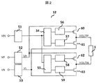
- FIG. 2 is a configuration example of the driver circuit 12 in the foreign matter inspection apparatus 100.
- the driver circuit 12 includes an input circuit 51, high voltage generation circuits 52 and 53, level shift circuits 54 and 55, MOS drive circuits 56, 57, 58 and 59, PMOS transistors 60 and 62, and NMOS transistors 61 and 63.
- a switching signal (VIN) from the data processing unit 11 is input to the input circuit 51 triggered by the presence or absence of a large-diameter foreign matter detected via the sensor 9 and the detection circuit 10, and the input circuit 51
- the PMOS transistors 60 and 62 and the NMOS transistors 61 and 63 are ON / OFF controlled through the level shift circuits 54 and 55 and the MOS drive circuits 56, 57, 58 and 59. Further, the high voltage generation circuits 52 and 53 generate voltages VH and VL based on the voltage control signals (VP and VN) from the data processing unit 11.
- VP is a voltage control signal for generating the voltage VH by the high voltage generation circuit 52
- VN is a voltage control signal for generating VL by the high voltage generation circuit 53.
- FIG. 3 shows an operation example of the driver circuit 12.
- the switching signal VIN is a binary signal having a Low and High potential, and the respective states are represented as L and H.
- VIN is L
- the PMOS transistor 60 is turned on through the level shift circuit 54 and the MOS drive circuit 56 from the input circuit 51
- the NMOS transistor 61 is turned off through the MOS drive circuit 57
- VOUTP has the same potential as VH. Become.
- the PMOS transistor 62 is turned off via the level shift circuit 55 and the MOS drive circuit 58, the NMOS transistor 63 is turned on via the MOS drive circuit 59, and VOUTN has the same potential as VL.
- VH ⁇ VL is applied to the optical modulation element 3.
- VIN is H
- the PMOS transistor 60 is OFF
- the NMOS transistor 61 is ON
- VOUTP is the same potential as VL
- the PMOS transistor 62 is ON
- the NMOS transistor 63 is OFF
- VOUTN is the same as VH.
- a potential difference of VL ⁇ VH is applied to the optical modulation element 3 in terms of potential.
- and offset voltage: (VH + VL) / 2 is applied to the modulation element 3.
- FIG. 4 is a block diagram showing a second embodiment of the driver circuit according to the present invention.
- symbol same as Example 1 is abbreviate
- the driver circuit 12 shown in FIG. 4 includes an input circuit 51, high voltage generation circuits 64 and 65, level shift circuits 54 and 55, MOS drive circuits 56, 57, 58, and 59, PMOS transistors 60 and 62, and NMOS transistors 61 and 63. Consists of.
- the high voltage generation circuit 64 generates a voltage based on the voltage control signal (VP) from the data processing unit 11 and is shifted using the VL generated by the high voltage generation circuit 65 as a reference voltage.
- the potential difference generated by the high voltage generation circuit 64 becomes the switching amplitude for the optical modulation element 3:
- the potential difference applied to the optical modulation element 3 is controlled only by the voltage control signal VP, and the offset voltage to the optical modulation element 3 is controlled only by the voltage control signal VN.
- FIG. 5 is a block diagram showing a third embodiment of the driver circuit according to the present invention.
- symbol same as Example 1 is abbreviate
- the driver circuit 12 shown in FIG. 5 includes a plurality of driver circuits 12a and 12b.
- the configurations of the driver circuits 12a and 12b are the same as the components described in the first embodiment.
- the input circuit 51 of the driver circuit 12a receives control signals VIN and EN1 from the data processing unit 11, and the high voltage generation circuits 52a and 53b receive VP1 and VN1, respectively.
- predetermined voltages VH1 and VL1 are generated by the high voltage generation circuits 52a and 53b, and whether or not the outputs of VOUTP1 and VOUTN1 are controlled by EN1.
- VOUTP1 and VOUTN1 select and output VH1 and VL1 according to VIN1.
- VOUTPn and VOUTNn are connected to one input of the optical modulation element 3, and VOUTN1 and VOUTNn are connected to the other input.
- the driver circuit 12 shown in FIG. 5 makes it possible for the driver circuit to select and apply an arbitrary voltage set in advance to the optical modulation element 3 under the control of the data processing unit 11.
- switching the voltage with the MOS transistors 60a to 63b can switch the applied voltage to the optical modulation element 3 at a higher speed than switching the voltage with the MOS transistors 60a to 63b, rather than variably controlling the voltage with the high voltage generation circuits 52a, 53a, 52b, 53b Irradiation laser power control at multiple levels during the wafer inspection period is possible.
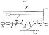
- FIG. 6 is a block diagram showing a fourth embodiment of the foreign matter inspection apparatus according to the present invention. Similarly to the above description, in order to avoid the description from becoming complicated, the description of the components having the same reference numerals as those in the first embodiment is omitted.
- the data processing unit 11 predicts the presence or absence of a large-diameter foreign substance, and controls voltage switching in the driver circuit 12.
- the polarization plane of the laser light that passes through the optical modulation element 3 is rotationally controlled by the predetermined voltage switched by the driver circuit 12, and the laser power that passes through the polarizing plate 4 is controlled.
- the laser power applied to the wafer 1 through the beam splitter 5 is detected by the optical power detection means 13, and the laser power output to the laser light source 2 is controlled based on the detection result. To do.
- the relationship between the rotation angle of the polarization plane and the laser power is not linear. For this reason, in order to obtain the desired laser power with high accuracy, depending on the polarization plane of the laser light, high-precision control of the voltage applied from the driver circuit 12 to the optical modulation element 3 is required, which increases the device cost. To do.
- the laser light source 2 as shown in the present embodiment, it is not necessary to provide high-cost high-accuracy voltage generation / control means in the driver circuit 12, and the performance wafer 1 is irradiated.
- the laser power can be controlled with high accuracy.
- a MOS transistor is used as the voltage switching means for the sake of explanation.
- other semiconductor switching elements, relays, etc. may be used. Switching control and power supply voltage as a connection source for these elements may be used. It goes without saying that the laser power to be irradiated to the wafer under inspection and the irradiation laser power stabilization for a long time can be realized by dynamically controlling.
- the binary voltage VH and VL is switched for the purpose of explanation.
- a plurality of driver circuits are provided to switch a plurality of voltages. It goes without saying that irradiation laser power control at a plurality of levels can be realized.
- a defect inspection apparatus for inspecting a defect on the sample surface by irradiating the sample surface with a laser for a predetermined time, a laser light source for emitting a laser beam irradiated on the sample surface, and the emitted light
- a modulation unit that modulates a laser beam
- a control unit that controls a voltage applied to the modulation unit
- a reflected light detection unit that detects scattered light reflected from the sample surface and generates a detection signal
- the control unit controls to switch the voltage applied to the modulation unit based on the detection result of the reflected light detection unit.
- a defect inspection apparatus for inspecting a defect on the sample surface by irradiating the sample surface with a laser for a predetermined time, a laser light source for emitting a laser beam irradiated on the sample surface, and the emitted light
- a modulation unit that modulates a laser beam
- a control unit that controls a voltage applied to the modulation unit
- a laser power detection unit that detects the laser power that is modulated and applied to the sample surface. Is a voltage applied to the modulation unit when the laser power of the first time and the laser power of the second time are different as a result of detection by the laser power detection unit at the first time and the second time.
- the defect inspection apparatus includes a laser power detection unit that detects the laser power that is modulated and applied to the sample surface, and the control unit includes a first time As a result of detection by the laser power detection unit at a second time, a defect inspection that controls a voltage applied to the modulation unit when the laser power at the first time differs from the laser power at the second time There is a device.
- the defect inspection apparatus As a fourth modification, the defect inspection apparatus according to the second or third modification, wherein the control unit generates a first voltage to be applied to the modulation unit based on a result detected by the laser power detection unit.
- the defect inspection method is characterized in that the control unit variably controls the voltage generated by the first voltage generation unit and the second voltage generation unit.
- the defect inspection apparatus according to any one of the first to third modifications, wherein the control unit includes a first voltage generation unit and a second voltage generation unit.
- the control unit includes a first voltage generation unit and a second voltage generation unit.
- a defect inspection apparatus characterized in that a potential difference between one voltage generation unit and the second voltage generation unit is applied to the modulation means.
- defect inspection apparatus As a sixth modification, there is a defect inspection apparatus according to any one of the first to third modifications, wherein the defect inspection apparatus includes a plurality of the control units.
- the defect inspection apparatus according to Modification 2 or 3 as Modification 7, wherein the control unit controls the laser power emitted from the laser light source based on the detection result of the laser power detection unit. There is a defect inspection device.
- a modification 8 is a defect inspection method for inspecting a defect on the sample surface by irradiating the sample surface with a laser for a predetermined time, a laser emission step for emitting a laser beam irradiated on the sample surface, and a voltage.
- a modulation step for applying and modulating the emitted laser beam, a control step for controlling a voltage applied in the modulation step, and a reflected light detection step for detecting scattered light reflected from the sample surface and generating a detection signal
- the control step there is a defect inspection method in which the voltage applied in the modulation step is controlled based on the detection result in the reflected light detection step.
- the modification 9 is the defect inspection method according to the modification 8, in which the laser power detection step of detecting the laser power that is modulated and applied to the sample surface, and the control step includes a first time and a first time
- a defect inspection method for controlling a voltage applied in the modulation step when the laser power in the first time and the laser power in the second time are different as a result of detection in the laser power detection step at a second time. is there.
- the modification 10 is the defect inspection method according to the modification 9, in which the control step generates a first voltage to be applied in the modulation step based on a result detected in the laser power detection step.
- a voltage generation step, a second voltage generation step of generating a second voltage, and a voltage switching step of switching the generated first voltage or the second voltage and applying in the modulation step In the control step, there is a defect inspection method characterized in that the voltage generated in the first voltage generation step and the second voltage generation step is variably controlled.
- the modification 11 is the defect inspection method according to the modification 8 or 9, wherein the control unit includes a first voltage generation step and a second voltage generation step, and the first voltage generation step and the second voltage generation step.
- the control unit includes a first voltage generation step and a second voltage generation step, and the first voltage generation step and the second voltage generation step.
- the defect inspection method according to the modification 9 is characterized in that, in the control step, the laser power emitted in the laser emission step is controlled based on the detection result in the laser power detection step. There is a defect inspection method.
- control lines and information lines indicate what is considered necessary for the explanation, and not all the control lines and information lines on the product are necessarily shown. Actually, it may be considered that almost all the components are connected to each other.
- the optical inspection apparatus widely includes apparatuses using a laser.
- the optical inspection apparatus includes a system in which the optical inspection apparatus is connected by a network and a composite apparatus of the charged particle beam apparatus, which are collectively referred to as an optical inspection system. is there.
- the “sample” widely includes a semiconductor wafer having a fine pattern, a wafer before pattern formation, a photomask (exposure mask), a liquid crystal substrate, and the like.
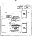
- FIG. 7 is a diagram showing a schematic configuration of an optical inspection apparatus 1 which is an example of a semiconductor inspection apparatus to which the present invention is applied.
- the optical inspection apparatus 7000 includes a transport system, a stage system, an optical system, and a data processing system, which are controlled by the overall control unit 100.
- the sample 7002 has a robot arm inside and is transported to a stage in the inspection chamber by a transfer device 701 adjacent to the inspection chamber, and is fixed to the stage by vacuum suction or an edge clip.
- the sample stage includes a rotary stage 702, a vertical axis stage 703, and a horizontal axis stage 704, which are controlled by a stage control unit 705.
- the vertical axis stage 703 uses a distance sensor (not shown) fixed to the reference plane of the illumination optical system 706 to match the focus surfaces of the illumination optical system 706 and the detection unit 707 with the sample surface. The entire surface of the sample can be inspected by moving the stage in the radial direction while rotating the stage.
- the optical system includes an illumination optical system 706 and a detection 707.
- the illumination optical system 706 includes a laser light source, a lens, and a stop, and details will be described later with reference to FIGS.
- the illumination optical system 706 modulates the illumination beam to an appropriate power, shapes the illumination beam to an appropriate spot size, and illuminates the sample 7002.
- the detection unit 707 includes a detection optical system including a plurality of lenses and a detector.
- the detection unit 707 collects scattered light from the sample 7002 on the detector, converts the light into an electric signal, and sends the electric signal to the signal processing unit 709.
- the illumination optical system 706 and the detection unit 707 are controlled by the optical system control unit 708, and adjust the arrangement of the optical elements and the gain of the detector according to the inspection conditions.
- the signal processing unit 709 appropriately processes the signal input from the detection unit 707 and determines a defect. At this time, the size of the defect is determined based on the intensity of the signal. Further, the coordinates of the defect are determined using encoder signals input from the rotary stage 702 and the horizontal axis stage 704.
- the data processed by the signal processing system unit 709 is transmitted to the overall control unit 700 and displayed on the display 710 or stored as a data file in the storage unit 711.
- the system configuration is not limited to this, and some or all of the devices constituting the system may be a common device.
- the overall control unit 700, the stage control unit 705, the optical system control unit 708, and the signal processing unit 709 can be realized by either hardware or software.
- it can be realized by integrating a plurality of arithmetic units for executing processing on a wiring board or in a semiconductor chip or package.
- CPU central processing unit
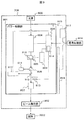
- FIG. 8 shows an example of the configuration of the illumination optical system 706.
- the illumination optical system includes a light source 800, a power control unit 801, and a beam shaping unit 802.
- the light source 800 for example, a laser light source is used.
- a high-power light source that oscillates a short-wavelength ultraviolet or vacuum ultraviolet laser beam and has an output of 1 W or more is used as a wavelength that does not easily penetrate into the sample.
- the beam shaping unit 802 is an optical unit that forms a predetermined illumination shape, and includes, for example, a beam expander.
- the power control unit 801 mainly includes a Pockels cell 804, a half-wave plate 805, a polarizing beam splitter 806, and an attenuator (static attenuator) 807.
- a Pockels cell is used as an example of an electro-optical element, but any element that can electrically switch the polarization direction of light may be used.
- the laser light incident on the Pockels cell 804 is phase-modulated according to the voltage applied from the Pockels cell control unit 808. Further, a certain amount of phase is modulated by a half-wave plate 805 disposed at the rear stage of the Pockels cell, and is incident on the polarization beam splitter 806.
- the half-wave plate 805 is placed in front of the polarizing beam splitter.
- the half-wave plate 805 is fixed to the rotary stage 818 and can be arranged at an arbitrary angle.
- the arrangement angle is controlled by the half-wave plate control unit 809.
- a half-wave plate arranged at 45 ° is used as an optical path with a linear motion stage or the like. It may be configured to be taken in and out.
- the light phase-modulated by the Pockels cell 804 and the half-wave plate 805 is branched into two optical paths by the polarization beam splitter 806.
- Light that passes through the polarizing beam splitter 806 is referred to as inspection light, and reflected light is referred to as non-inspection light.
- the ratio of inspection light to non-inspection light can be adjusted by the Pockels cell applied voltage and the arrangement angle of the half-wave plate.
- Non-inspection light passes through the beam sampler 810 and enters the diffuser 811.
- the beam sampler 810 an element in which reflected light is larger than transmitted light is used.
- a part of the light reflected by the beam sampler 810 is incident on the power monitor 812 to constantly monitor its power level.
- the power monitor signal is input to the Pockels cell control unit 808 and used to optimize the Pockels cell applied voltage and detect Pockels cell abnormality.
- the Pockels cell control unit 808 includes an interlock circuit that compares the control signal with the power monitor signal and closes the optical path shutter 813 when power that does not match the control signal is detected.
- the maximum value of the irradiation power is limited by the attenuator 807 at the end of the power control unit, and even when intensity control by the Pockels cell becomes uncontrollable, the irradiation power to the sample can be limited to realize fail safe. ing.
- the power control unit 201 is provided with a thermometer 815 and a heater 816, and is managed at a constant temperature by the temperature control unit 817.
- a cooler may be used instead of the heater 816, and a function of performing both heating and cooling may be provided.
- FIG. 9 shows another example of the configuration of the illumination optical system 706.
- 8 is a configuration in which a beam sampler 910 is disposed on the optical path of the inspection light and a part of the inspection light is monitored by the power monitor 812.
- the beam sampler 910 an element in which transmitted light is larger than reflected light is used.
- the optical path shutter 813 is arranged at a stage subsequent to the beam sampler 810.
- the inspection light is branched and monitored, so that the state of the inspection light can be grasped more directly.
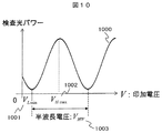
- FIG. 10 shows the relationship between Pockels cell applied voltage and inspection power (intensity modulation characteristics).
- the polarization axis rotates with respect to the transmission axis of the polarization beam splitter 806, so that a voltage characteristic (intensity modulation characteristic) 1000 as shown in FIG. 10 is obtained.
- the voltage VLmin 1001 When the voltage VLmin 1001 is applied, it rotates 90 degrees with respect to the transmission axis of the polarizing beam splitter 806, and the inspection light power is minimized.
- the voltage VHmax 1002 When the voltage VHmax 1002 is applied, the polarization axis coincides with the transmission axis of the polarization beam splitter 806, and the inspection light power is maximized.
- the voltage at which the polarization axis rotates 180 ° is called a half-wave voltage VHW1003, which is an indicator of the voltage characteristics of the Pockels cell.
- FIG. 11A shows an example of the Pockels cell applied voltage.
- the Pockels cell applied voltage has a reference first level VL1101 and a second level VH1102. This level can be arbitrarily specified by the Pockels cell control unit. For example, if the first level is set to the voltage VLmin that minimizes the inspection light power and the second level is set to the voltage VHmax that maximizes the inspection light power, the applied voltage is switched between VLmin and VHmax. The power can be switched.
- the ratio between the minimum power and the maximum power is determined by the extinction ratio of the Pockels cell, and is generally 1:50 to 1: 1000. For example, when a Pockels cell with an extinction ratio of 1:50 is used, the maximum power can be set to 100% and the power can be switched to 2%.
- any power between 2% and 100% can be extracted.
- a large foreign object is on the sample surface and its position is known in advance by any method, switching the control voltage in the vicinity of the large foreign object to lower the inspection power, while suppressing the explosion of the large foreign object,
- the area can be inspected with high sensitivity by increasing the inspection power.
- a method of detecting a large foreign material in advance a method of performing a preliminary inspection before the main inspection, a method of detecting immediately before using an end portion of the inspection light beam, or the like can be considered.
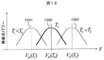
- FIG. 12 shows how the voltage characteristics of the Pockels cell change with temperature.
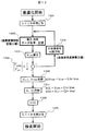
- FIG. 13 is a diagram for explaining a voltage correction flow.
- the optical path shutter 813 is closed to prevent erroneous irradiation (step 1301).
- the non-inspection optical power data is obtained by changing the voltage applied to the Pockels cell in a certain range and pitch, and the intensity modulation characteristic storage unit shown in FIGS. (Step 1302, intensity modulation characteristic storing step).
- VLmin is obtained from the acquired voltage characteristic data (step 1305). Whether or not the obtained VLmin value satisfies the conditional expression 1304 is confirmed. If not, the arrangement angle of the half-wave plate is changed (step 1305, wave plate angle adjustment step), and optimization is performed again.
- conditional expression 1304 is a condition for suppressing the inspection light power to 50% or less of the maximum power when the voltage is applied (the reason why it can be suppressed to 50% or less is shown in FIG. 8).
- VHmax is calculated from VLmin and registered as a constant representing the voltage characteristic of the Pockels cell (step 1306).
- the calculation formula here is based on the relationship shown in FIG. From these VLmin and VHmax, VL and VH actually used as control voltages are obtained and registered (step 1307).
- the fixed values 1 and 2 when calculating VL and VH are constants determined by how much the minimum and maximum power are to be set, respectively.
- VL is set as the voltage value at the start of the inspection (step 1308), and after the safe state is prepared, the shutter is opened (step 1309) and the inspection is started.
- step 1302 by always performing the voltage correction flow shown in FIG. 13, particularly the intensity modulation characteristic storing step (step 1302), before the inspection, the effect of the above-described relatively short-term temperature fluctuation is expressed as fluctuation of the voltage characteristic of the Pockels cell. Therefore, the influence of the temperature variation can be corrected by applying a voltage to the Pockels cell at the time of inspection based on the stored intensity modulation characteristic.
- inspection is performed by illuminating the sample 7002 with laser light from the illumination optical system 706, receiving scattered light from the sample 7002 by the detection unit 707, and then determining defects by the signal processing unit 709. This shows that the sample 7002 is being executed.
- the term “before inspection” includes not only before the inspection is performed, that is, immediately after the sample 7002 is transported into the inspection chamber, but also before the next predetermined inspection after the predetermined inspection is completed.
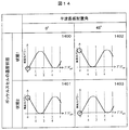
- the table in FIG. 14 shows that the inspection power when the applied voltage becomes 0 can be suppressed to 50% or less of the maximum power when the voltage is always applied by the rotary wave plate (wave plate angle adjustment step). It is for explanation.
- the horizontal axis is a value obtained by normalizing the applied voltage with a half-wave voltage, and the vertical axis is the inspection light power.
- State 1 and state 2 indicate different temperature states.
- the half-wave plate when the temperature is in state 1, the half-wave plate is 0 ° so that the characteristic is 1400, and when the temperature is state 2, the half-wave plate is 45 ° so that the characteristic is 1403. .
- an offset may be added to the phase with a wave plate so that the inspection light power is minimized (preferably 0) when the voltage applied to the Pockels cell is zero.
- the transmitted power is reduced to 50% or less of the maximum power with the voltage applied. Can be limited. Thereby, the risk of damaging the sample 7002 can be minimized.
- the voltage characteristic data acquisition / storage 1302 (intensity modulation characteristic storage step) before the inspection shown in FIG. 13 or the VLmin and VHmax registration 1306 associated therewith can be compared with a relatively short period of time that changes for each inspection.
- the effect of temperature fluctuations can be corrected, thereby not only suppressing explosions of large foreign objects with high accuracy but also maximizing the inspection light power during normal inspection with high accuracy and improving inspection sensitivity. .
- control lines and information lines indicate what is considered necessary for the explanation, and not all the control lines and information lines on the product are necessarily shown. Actually, it may be considered that almost all the components are connected to each other.
- Sample 706 Lighting Academic system 800 ... light source 804 ... Pockels cell 805 ... half-wave plate (wave plate) 806 ... polarizing beam splitter 807 ... static attenuator 808 ... Pockels cell control unit 809 ... Half-wave plate control unit 812 ... power monitor 814 ... intensity modulation characteristic storage unit 1000 ... intensity modulation characteristic 1302 ... intensity modulation characteristic storage step 1305 ... wave plate angle adjustment step.
Landscapes
- General Health & Medical Sciences (AREA)
- Health & Medical Sciences (AREA)
- Life Sciences & Earth Sciences (AREA)
- Chemical & Material Sciences (AREA)
- Analytical Chemistry (AREA)
- Biochemistry (AREA)
- Physics & Mathematics (AREA)
- General Physics & Mathematics (AREA)
- Immunology (AREA)
- Pathology (AREA)
- Testing Or Measuring Of Semiconductors Or The Like (AREA)
- Investigating Materials By The Use Of Optical Means Adapted For Particular Applications (AREA)
- Optical Modulation, Optical Deflection, Nonlinear Optics, Optical Demodulation, Optical Logic Elements (AREA)
Abstract
本発明は、高精度な異物検出が可能な検査装置を提供するものであって、検査装置を、光源と、この光源からの光が入射され、この光の位相を少なくとも2状態に変化させる電気光学素子と、制御部と、を有し、制御部は、電気光学素子へ入力する印加電圧を変化させることで得られた電気光学素子の強度変調特性を使用し、電気光学素子自体が有する位相変動を補正するように構成した。
Description
本発明は、微小異物を検査する検査装置に関する。
本技術分野の背景技術として、特表2009-501902号公報(特許文献1)がある。この公報には、「検査システムの測定検出範囲の制限要因として増幅器及びアナログ・デジタル回路の飽和レベルに対処することによって欠陥検出を強化するための検査システム、回路及び方法も提供される。加えて、表面検査の走査の間に試料に供給される入射レーザ・ビームパワー・レベルを動的に変更することによって大きな粒子に対する熱破損を削減することにより欠陥検出を強化するための検査システムや回路、方法が提供される。」と記載されている(要約参照)。
また、前記のポッケルスセルを駆動する手段としては、例えば、特開2001-144357号公報(特許文献2)で述べられているように、ポッケルスセルに対して所定の電圧を切り替えて印加する手段が述べられている。
更に、半導体ウェーハの異物検査装置はウェーハ表面に存在する微小な欠陥を検出し、その個数、座標、大きさを出力する。半導体プロセスの微細化に伴い、異物検査装置には検出感度の向上が要求される。検出感度を向上させる手段のひとつとして、照明光の強度を高くする方法があった。しかし高い照明光強度で照射すると数百nmを越える大異物は破壊される。本明細書ではこの現象を爆裂と称する。爆裂によって生じた破片は、試料表面に拡散し、試料の不良領域を拡大するため、検査パワー(検査に用いる照明光の強度)を制限しなければならなかった。
米国特許第7787114号明細書(特許文献3)には、ポッケルスセルを用いて検査中に動的に検査パワーを制御する技術が開示されている。特許文献1では通常は高パワー照射によって高い感度で検査しながら、大きな異物が存在する場合はその異物及びその周辺だけ検査パワーを下げて爆裂を回避している。
微小異物の検査装置を長時間にわたって運用する場合、ポッケルスセルを通過するレーザパワーの影響で結晶の特性が変化する。この特性変化により、ポッケルスセルを通過するレーザの偏波面の回転角が変化し、試料であるウェハに照射するレーザパワーが変動する可能性がある。このため、ウェハ上の異物からの散乱光強度が変化し、高精度な異物径の検出が困難となるが、この点については特許文献1及び2においては考慮されていなかった。
また、特許文献3のように、高パワーのレーザ照射によって高い感度で検査する場合には、ポッケルスセル自体あるいはポッケルスセル制御部が故障して異常停止した場合、試料に過大なパワーのレーザが照射されてしまう可能性がある。先行技術ではこの点について考慮されていなかった。
さらに、ポッケルスセル自体の温度状態により制御電圧が変わってしまうため、予め決められた電圧を印加しても意図したレーザパワーに制御できない可能性がある。つまり、ポッケルスセル自体の電圧特性の変化により、意図せずして過大なパワーのレーザが試料に照射されてしまう可能性がある。
そこで、本発明は、高精度な異物検出が可能な検査方法および検査装置を提供する。
また本発明では、ポッケルスセルなどの電気光学素子を用いてレーザパワーの制御をする装置において、レーザパワーを安全に制御できるようにすることを目的とする。
上記課題を解決するために、例えば特許請求の範囲に記載の構成を採用する。
本願は上記課題を解決する手段を複数含んでいるが、その一例を挙げるならば、検査装置を、光源と、この光源からの光が入射され、この光の位相を少なくとも2状態に変化させる電気光学素子と、制御部と、を有し、制御部は、電気光学素子へ入力する印加電圧を変化させることで得られた電気光学素子の強度変調特性を使用し、電気光学素子自体が有する位相変動を補正するように構成した。
本発明によれば、微小な異物を高精度に検出することが出来る。
また、本発明によれば、パワー制御システムが故障した場合であっても試料にダメージを与えるリスクを最小化できる。
上記した以外の課題、構成及び効果は、以下の実施形態の説明により明らかにされる。
本発明は、試料表面にレーザを所定の時間照射して試料表面の欠陥を検査する検査装置に関するもので、試料表面に照射されるレーザビームを出射するレーザ光源と、出射したレーザビームを変調する変調部と、この変調部に印加する電圧を制御する制御部と、試料表面から反射した散乱光を検出して検出信号を生成する反射光検出部とを備え、制御部は、反射光検出部での検出結果に基づき、変調部に印加する電圧を切替えるよう制御するように構成したものである。
また本発明は、レーザ光により試料を検査する検査装置において、レーザ光を射出するレーザ光源と、このレーザ光源からのレーザ光が入射され、レーザ光の位相を少なくとも2状態に変化させる電気光学素子と、レーザ光の位相を回転させる波長板と、を有する照明光学系を有し、波長板は、電気光学素子に電圧を印加しない状態で、試料に照射されるレーザ光の強度が、電気光学素子に電圧を印加した状態での最大強度よりも減衰されるような位相差を発生させるように構成したものである。
以下、実施例を図面を用いて説明する。
本実施例では、検査中でのウェハに照射するレーザパワーを切り替えるとともに、長時間での照射レーザパワーを安定化する異物検査装置の例を説明する。
図1は、本実施例の異物検査装置の構成図の例である。
異物検査装置100は、レーザ光源2、光学変調素子3、偏光板4、ビームスプリッタ5、ミラー6、レンズ7、8、センサ9、検出回路10、データ処理部11、ドライバ回路12、光パワー検出手段13、ステージ14を有する。
異物検査装置100では、ウェハ1をステージ14上に設置して、レーザ光源2から出力されるレーザ光を光学変調素子3、偏光板4、ビームスプリッタ5、ミラー6、レンズ7を介してウェハ1上に照射する。このとき、異物検査装置100では、ステージ14でウェハ1を回転動作させるとともに、並進ステージ(図示せず)で直線動作させ、これにより、ウェハ1上に照射されるレーザ光は、ウェハ1の全面でらせん状の軌跡となり、ウェハ1の全表面を検査することができる。また、ウェハ1上の異物からの散乱光は、レンズ8、センサ9、検出回路10を介して検出され、前記検出回路10の検出結果を元にデータ処理部11で異物判定が行われる。
本実施例による異物検査装置100では、ドライバ回路12は、データ処理部11からの切替制御により光学変調素子3への印加電圧を切替える。データ処理部11は、ウェハ上をらせん状に走査した前周での検出結果に基づいて大径異物の有無を予測し、ドライバ回路12での電圧切替を制御する。具体的には、データ処理部11で大径異物があると予測した場合、ウェハ1に照射するレーザパワーを小さくする。
ドライバ回路12で切り替えられた所定の電圧により、光学変調素子3は、通過するレーザ光の偏波面を回転制御し、偏光板4を通過するレーザパワーを制御する。具体的には、データ処理部11において大径異物があると予測した場合、ウェハ1に照射するレーザパワーを小さくする所定の電圧をドライバ回路12が出力するようにするとともに、大径異物がないと予測する場合はレーザパワーを大きくする所定の電圧をドライバ回路12が出力する。
またデータ処理部11では、ビームスプリッタ5を介してウェハ1に照射されるレーザパワーを光パワー検出手段13で検出し、前記検出結果に基づいて、前記ドライバ回路12で切り替えて前記光学変調素子3に出力される電圧値を制御する。これは、光学変調素子3が温度等の環境条件によって、ドライバ回路12から同一の制御電圧を印加しても、光学変調素子3を通過するレーザ光の偏波面の回転角が異なり、その結果としてウェハ1に照射するレーザパワーが変動するためである。レーザパワーが変動するとウェハ1上にある異物の検出精度が悪化するため、光パワー検出手段13を介して所定のレーザパワーがウェハ1に照射されるよう、ドライバ回路12で切り替える電圧を制御することで異物の検出精度を向上させる。
図2は、異物検査装置100におけるドライバ回路12の構成例である。
ドライバ回路12は、入力回路51、高圧発生回路52、53、レベルシフト回路54、55、MOS駆動回路56、57、58、59、PMOSトランジスタ60、62、NMOSトランジスタ61、63で構成される。
ドライバ回路12では、前記センサ9および検出回路10を介して検出される大径異物の有無を契機として前記データ処理部11からの切替信号(VIN)が入力回路51に入力され、前記入力回路51からレベルシフト回路54、55とMOS駆動回路56、57、58、59を介して、PMOSトランジスタ60、62、NMOSトランジスタ61、63がON/OFF制御される。さらに、前記データ処理部11からの電圧制御信号(VP、VN)により、高圧発生回路52、53でVH、VLの電圧が生成される。ここでVPは高電圧発生回路52でVHの電圧を生成するための電圧制御信号であり、VNは高電圧発生回路53でVLを生成するための電圧制御信号である。また、PMOSトランジスタ60、62、NMOSトランジスタ61、63に印加する電位関係から、高電位となる電圧をVH、低電位となる電圧をVLとする。
図3は、ドライバ回路12の動作例である。切替信号であるVINはLow,Highの電位を有する2値信号であり、それぞれの状態をL,Hとして表す。VINがLのとき入力回路51から、レベルシフト回路54と、MOS駆動回路56を介してPMOSトランジスタ60がON、MOS駆動回路57を介してNMOSトランジスタ61がOFFとなり、VOUTPはVHと同電位となる。
また同時に、レベルシフト回路55と、MOS駆動回路58を介してPMOSトランジスタ62がOFF、MOS駆動回路59を介してNMOSトランジスタ63がONとなり、VOUTNはVLと同電位となる。この結果、光学変調素子3にはVH-VLの電位差が印加される。
一方で、VINがHのときは、PMOSトランジスタ60がOFF、NMOSトランジスタ61がONで、VOUTPはVLと同電位、また、PMOSトランジスタ62がON、NMOSトランジスタ63がOFFとなり、VOUTNはVHと同電位で、光学変調素子3にはVL-VHの電位差が印加される。
前記データ処理部11からの電圧制御信号(VP、VN)に基づいて、高圧発生回路52、53でそれぞれVH=V1、VL=V3、またはVH=V2、VL=V4を生成することにより、光学変調素子3には、切替振幅:|VH-VL|、オフセット電圧:(VH+VL)/2の電圧が印加される。
光パワー検出手段13の検出結果に基づいてデータ処理部11から電圧制御信号(VP、VN)を介して光学変調素子3に印加する切替振幅とオフセット電圧を調整することで、光学変調素子3の特性変動を補正し、ウェハ1に照射する長時間でのレーザパワー変動を抑制することが実現できる。
本実施例の構成により、検査中でのウェハに照射するレーザパワーを切り替えるとともに、長時間での照射レーザパワーを安定化することにより微小な異物を正確に検出することが出来る。なお、この効果は、以下に説明する実施例においても同様である。
図4は、本発明に係るドライバ回路について、第2の実施形態を示す構成図である。なお、説明が煩雑になることを避けるため、実施例1と同一の符号をつけた構成要素についての説明は省略する。
図4で示したドライバ回路12は、入力回路51、高圧発生回路64、65、レベルシフト回路54、55、MOS駆動回路56、57、58、59、PMOSトランジスタ60、62、NMOSトランジスタ61、63で構成される。高圧発生回路64は、データ処理部11からの電圧制御信号(VP)による電圧を生成し、高圧発生回路65で生成されたVLを基準電圧としてシフトされる。高圧発生回路64で生成された電位差が光学変調素子3に対する切替振幅:|VH-VL|となる。本実施形態では、光学変調素子3に与える電位差は電圧制御信号VPのみで制御するとともに、光学変調素子3へのオフセット電圧は電圧制御信号VNのみで制御する。これにより、電位差もしくはオフセット電圧の一方のみを変化させることが可能となり、データ処理部11から光学変調素子3に対する制御方法が簡便となる。
図5は、本発明に係るドライバ回路について、第3の実施形態を示す構成図である。なお、説明が煩雑になることを避けるため、実施例1と同一の符号をつけた構成要素についての説明は省略する。
図5で示したドライバ回路12は、複数のドライバ回路12a、12bで構成される。ドライバ回路12a、12bのそれぞれの構成については、実施例1で説明した構成要素と同一構成である。ドライバ回路12aの入力回路51はデータ処理部11からの制御信号VIN、EN1が入力され、高圧発生回路52a、53bはそれぞれVP1、VN1が入力される。
ドライバ回路12aでは、高圧発生回路52a、53bにより所定の電圧VH1、VL1が生成され、EN1でVOUTP1、VOUTN1の出力可否が制御される。EN1で出力可となった場合、VOUTP1、VOUTN1はVIN1に応じてVH1、VL1を選択出力する。
同様にドライバ回路12bにおいても、データ処理部11からの制御信号VIN、ENnおよびVPn、VNnに応じて、VOUTPn、VOUTNnの出力可否とVHn、VLnの選択出力を行う。光学変調素子3の一方の入力にはドライバ回路12a、12bからのVOUTP1、VOUTPnが接続されるとともに、他方の入力にはVOUTN1、VOUTNnが接続される。
図5で示したドライバ回路12により、データ処理部11からの制御でドライバ回路はあらかじめ設定した任意の電圧を選択して光学変調素子3に印加することが可能となる。一般的に、高圧生成回路52a、53a、52b、53bで電圧を可変制御するよりも、MOSトランジスタ60a~63bで電圧を切り替えるほうが、光学変調素子3に対して高速に印加電圧を切替制御でき、ウェハ検査期間中における複数レベルでの照射レーザパワー制御が可能となる。
図6は、本発明に係る異物検査装置について、第4の実施形態を示す構成図である。上記の説明と同様に、説明が煩雑になることを避けるため、実施例1と同一の符号をつけた構成要素についての説明は省略する。
図6で示した異物検査装置100は、データ処理部11で大径異物の有無を予測し、ドライバ回路12での電圧切替を制御する。ドライバ回路12で切り替えられた所定の電圧により、光学変調素子3を通過するレーザ光の偏波面を回転制御し、偏光板4を通過するレーザパワーを制御する。またデータ処理部11では、ビームスプリッタ5を介してウェハ1に照射されるレーザパワーを光パワー検出手段13で検出し、前記検出結果に基づいて、レーザ光源2に対して出力するレーザパワーを制御する。
光学変調素子3と偏光板4のみを用いてレーザ光の偏波面を回転制御してレーザパワーを制御する場合、偏波面の回転角とレーザパワーとの関係は線形にならない。このため、所期のレーザパワーを高精度に得るためには、レーザ光の偏波面によっては、ドライバ回路12から光学変調素子3に印加する電圧の高精度な制御が必要となり、装置コストが増大する。
これに対して、本実施形態に示すようにレーザ光源2を組合せることで、ドライバ回路12において高コストな高精度な電圧生成・制御手段を配設する必要が無くなり、性能ウェハ1に照射するレーザパワーを高精度に制御することが可能となる。
なお、上記では説明のため電圧切替手段としてMOSトランジスタを用いて説明したが、他の半導体スイッチング素子やリレー等を用いてもよく、これらの素子に対して切替制御と、接続元となる電源電圧を動的に制御することにより、検査中でのウェハに照射するレーザパワー切り替えと長時間での照射レーザパワー安定化が実現できることは言うまでもない。
また、上記では説明のためVH、VLなる2値の電圧を切り替えることで説明したが、実施例3で説明したように、複数のドライバ回路を配設することにより、複数の電圧を切り替えることで複数レベルでの照射レーザパワー制御が実現できることは言うまでもない。
また、本発明は上記した実施例に限定されるものではなく、様々な変形例が含まれる。
例えば、上記した実施例は本発明を分かりやすく説明するために詳細に説明したものであり、必ずしも説明した全ての構成を備えるものに限定されるものではない。また、ある実施例の構成の一部を他の実施例の構成に置き換えることが可能であり、また、ある実施例の構成に他の実施例の構成を加えることも可能である。また、各実施例の構成の一部について、他の構成の追加・削除。置換をすることが可能である。具体的な変形例としては、以下のとおりである。
変形例1として、試料表面にレーザを所定の時間照射して前記試料表面の欠陥を検査する欠陥検査装置であって、前記試料表面に照射されるレーザビームを出射するレーザ光源と、前記出射したレーザビームを変調する変調部と、前記変調部に印加する電圧を制御する制御部と、前記試料表面から反射した散乱光を検出して検出信号を生成する反射光検出部と、を備え、前記制御部は、前記反射光検出部での検出結果に基づき、前記変調部に印加する電圧を切替えるよう制御する、欠陥検査装置がある。
変形例2として、試料表面にレーザを所定の時間照射して前記試料表面の欠陥を検査する欠陥検査装置であって、前記試料表面に照射されるレーザビームを出射するレーザ光源と、前記出射したレーザビームを変調する変調部と、前記変調部に印加する電圧を制御する制御部と、前記変調されて試料表面に照射されるレーザパワーを検出するレーザパワー検出部と、を備え、前記制御部は、第一の時間と第二の時間に前記レーザパワー検出部で検出した結果、前記第一の時間のレーザパワーと前記第二の時間のレーザパワーが異なる場合に前記変調部に印加する電圧を制御する、欠陥検査装置がある。
変形例3として変形例1に記載の欠陥検査装置であって、前記変調されて試料表面に照射されるレーザパワーを検出するレーザパワー検出部と、を備え、前記制御部は、第一の時間と第二の時間に前記レーザパワー検出部で検出した結果、前記第一の時間のレーザパワーと前記第二の時間のレーザパワーが異なる場合に前記変調部に印加する電圧を制御する、欠陥検査装置がある。
変形例4として、変形例2または3に記載の欠陥検査装置であって、前記制御部は、前記レーザパワー検出部で検出した結果に基づき、前記変調部に印加する第一の電圧を生成する第一電圧生成部と、第二の電圧を生成する第二電圧生成部と、前記生成した第一の電圧または第二の電圧を切り替えて前記変調部に印加する電圧切替部と、を有し、前記制御部は、前記第一電圧生成部と前記第二電圧生成部で生成する電圧を可変制御する、ことを特徴とする欠陥検査方法がある。
変形例5として、変形例1ないし3のいずれか一項に記載の欠陥検査装置であって、前記制御手段は、第一の電圧生成部と第二の電圧生成部とを有し、前記第一電圧生成部と前記第二電圧生成部との電位差を前記変調手段に印加する、ことを特徴とする欠陥検査装置がある。
変形例6として、変形例1ないし3のいずれか一項に記載の欠陥検査装置であって、前記制御部を複数個備えることを特徴とする欠陥検査装置がある。
変形例7として変形例2または3に記載の欠陥検査装置であって、前記制御部は、前記レーザパワー検出部での検出結果に基づいてレーザ光源から出射するレーザパワーを制御することを特徴とする、欠陥検査装置がある。
変形例8として、試料表面にレーザを所定の時間照射して前記試料表面の欠陥を検査する欠陥検査方法であって、前記試料表面に照射されるレーザビームを出射するレーザ出射ステップと、電圧を印加して前記出射したレーザビームを変調する変調ステップと、前記変調ステップで印加する電圧を制御する制御ステップと、前記試料表面から反射した散乱光を検出して検出信号を生成する反射光検出ステップと、を備え、前記制御ステップでは、前記反射光検出ステップでの検出結果に基づき、前記変調ステップで印加する電圧を切替えるよう制御する、欠陥検査方法がある。
変形例9として、変形例8に記載の欠陥検査方法であって、前記変調されて試料表面に照射されるレーザパワーを検出するレーザパワー検出ステップと、前記制御ステップでは、第一の時間と第二の時間に前記レーザパワー検出ステップで検出した結果、前記第一の時間のレーザパワーと前記第二の時間のレーザパワーが異なる場合に前記変調ステップで印加する電圧を制御する、欠陥検査方法がある。
変形例10として、変形例9に記載の欠陥検査方法であって、前記制御ステップは、前記レーザパワー検出ステップで検出した結果に基づき、前記変調ステップで印加する第一の電圧を生成する第一電圧生成ステップと、第二の電圧を生成する第二電圧生成ステップと、前記生成した第一の電圧または第二の電圧を切り替えて前記変調ステップで印加する電圧切替ステップと、を有し、前記制御ステップでは、前記第一電圧生成ステップと前記第二電圧生成ステップで生成する電圧を可変制御する、ことを特徴とする欠陥検査方法がある。
変形例11として、変形例8または9に記載の欠陥検査方法であって、前記制御手段は、第一電圧生成ステップと第二電圧生成ステップを有し、前記第一電圧生成ステップと前記第二電圧生成ステップとの電位差を前記変調ステップで印加する、ことを特徴とする欠陥検査方法がある。
変形例12として、変形例9に記載の欠陥検査方法であって、前記制御ステップでは、前記レーザパワー検出ステップでの検出結果に基づいてレーザ出射ステップで出射するレーザパワーを制御することを特徴とする、欠陥検査方法がある。
また、制御線や情報線は説明上必要と考えられるものを示しており、製品上必ずしも全ての制御線や情報線を示しているとは限らない。実際には殆ど全ての構成が相互に接続されていると考えてもよい。
以下、実施例5として、光学式検査装置を用いた半導体検査装置の例を説明するが、これは本発明の単なる一例であって、本発明は以下説明する実施の形態に限定されるものではない。本発明において光学式検査装置とはレーザを用いた装置を広く含むものとする。また、以下で光学式検査装置とは、上記の光学式検査装置がネットワークで接続されたシステムや上記の荷電粒子線装置の複合装置も含むものとし、これらを総称し光学式検査システムと称することもある。
本実施例において、「試料」とは微細なパターンを有する半導体ウェーハ、パターン形成前ウェーハ、ホトマスク(露光マスク)、または液晶基板等を広く含むものとする。
図7は本発明が適用される半導体検査装置の一例である光学式検査装置1の概略構成を示す図である。光学式検査装置7000は、搬送系、ステージ系、光学系、データ処理系で構成されており、それらは全体制御部100によって制御される。
試料7002は、内部にロボットアームを備え検査室に隣接する搬送装置701によって検査室内のステージまで運ばれ、真空吸着またはエッジクリップによってステージに固定される。
試料ステージは、回転ステージ702、垂直軸ステージ703、水平軸ステージ704で構成され、これらはステージ制御部705によって制御される。垂直軸ステージ703は照明光学系706の基準面に固定された距離センサ(図示せず)を用いて、照明光学系706及び検出部707のフォーカス面と試料表面を一致させる。そして、ステージを回転させながら径方向に移動させることで、試料全面を検査することができる。
光学系は照明光学系706と検出707で構成される。照明光学系706はレーザー光源、レンズ、絞りを含んで構成されるものであり、詳細は図8および図9を用いて後述する。照明光学系706は照明ビームを適切なパワーに変調し、また照明ビームを適切なスポットサイズに成形し、試料7002を照明する。検出部707は複数のレンズからなる検出光学系及び検出器で構成され、試料7002からの散乱光を検出器に集光し、電気信号に変換して信号処理部709に送る。照明光学系706及び検出部707は光学系制御部708によって制御され、検査条件に応じて光学素子の配置、検出器のゲインを調整する。
信号処理部709は検出部707から入力された信号を適切に処理し、欠陥判定する。このとき信号の強度に基づいて欠陥のサイズを決定する。また、さらに回転ステージ702及び水平軸ステージ704から入力されるエンコーダ信号を用いて欠陥の座標を決定する。
信号処理系部709で処理されたデータは全体制御部700へ送信され、ディスプレイ710に表示または記憶部711にデータファイルとして保存される。
システムの構成はこれに限られず、システムを構成する装置の一部または全部が共通の装置であってもよい。
なお、全体制御部700、ステージ制御部705、光学系制御部708、信号処理部709は、ハードウェア、ソフトウェアいずれの方式でも実現可能である。ハードウェアにより構成する場合には、処理を実行する複数の演算器を配線基板上、または半導体チップもしくはパッケージ内に集積することにより実現できる。ソフトウェアにより構成する場合には、システムを構成する装置に搭載された中央演算処理装置(CPU)またはシステムに接続された汎用のコンピュータに搭載された汎用CPUにより、所望の演算処理を実行するプログラムを実行することで実現できる。
図8に、照明光学系706の構成の一例を示す。照明光学系は光源800とパワー制御部801、ビーム整形部802によって構成される。
光源800は、例えばレーザ光源が用いられる。試料表面近傍の微小な欠陥を検出するには、試料内部に浸透しづらい波長として、短波長の紫外または真空紫外のレーザビームを発振し、かつ出力1W以上の高出力の光源が用いられる。
ビーム整形部802は、所定の照明形状を形成する光学ユニットであり、例えばビームエキスパンダを含んで構成される。
パワー制御部801はポッケルスセル804、半波長板805、偏光ビームスプリッタ806、減衰器(静的アッテネータ)807によって主に構成される。なお、以下では電気光学素子の一例としてポッケルスセルを使用する例で説明するが、電気的に光の偏光方向を切り替えられる素子であればよい。ポッケルスセル804に入射したレーザ光はポッケルスセル制御部808からの印加電圧に応じて位相変調される。さらにポッケルスセル後段に配置された半波長板805によって一定量位相変調されて偏光ビームスプリッタ806へ入射する。ここで半波長板805が偏光ビームスプリッタの前段に入っていることが重要である。半波長板805は回転式ステージ818に固定されており、任意の角度に配置できるようになっている。配置角度は半波長板制御部809によって制御される。本実施例で使用する配置角度は0°及び45°の2種であり、この2種の配置角度の位相変調効果を得るためには、45°配置の半波長板を直動ステージ等で光路に出し入れする構成であってもよい。
ポッケルスセル804及び半波長板805によって位相変調された光は、偏光ビームスプリッタ806で2つの光路に分岐される。偏光ビームスプリッタ806を透過する光を検査光、反射される光を非検査光と称する。検査光と非検査光の比率はポッケルスセル印加電圧と半波長板の配置角度によって調整することができる。
非検査光はビームサンプラ810透過してデフューザ811に入射させる。ここでビームサンプラ810としては反射光の方が透過光より大きくなるような素子を用いる。ビームサンプラ810で反射させた一部の光はパワーモニタ812に入射させてそのパワーレベルを常時監視する。
パワーモニタ信号はポッケルスセル制御部808に入力し、ポッケルスセル印加電圧を最適化するため、またポッケルスセルの異常を検知するために使用する。
ポッケルスセル制御部808には制御信号とパワーモニタ信号を比較し、制御信号と一致しないパワーを検知した場合には、光路シャッタ813を閉めるインタロック回路が備わっている。
光路シャッタ813をパワーモニタ812への分岐を形成する偏光ビームスプリッタ806より後段に配置することで、試料7002を照明する前に正しく制御しているかを確認することができる。
さらにパワー制御部最終端の減衰機807で照射パワーの最大値を制限しており、ポッケルスセルによる強度変調が制御不能になった場合においても、試料への照射パワーを制限できフェールセーフを実現している。
ポッケルスセル804は温度によって特性が変化するためパワー制御部201には温度計815と加熱器816が備えられ、温度制御部817によって一定温度に管理されている。加熱器816の代わりに冷却器であってもよいし、加熱と冷却の両方を行う機能を有していてもよい。
以上により、比較的長期の温度変動に対して、一定温度管理の対応が可能となり、検査装置性能の信頼性向上に効果がある。
図9に照明光学系706の構成の別の一例を示す。図8と異なる部分は、検査光の光路上にビームサンプラ910を配置して検査光の一部をパワーモニタ812にて監視する構成である。ここでビームサンプラ910としては透過光の方が反射光より大きくなるような素子を用いる。この場合、光路シャッタ813はビームサンプラ810より後段に配置する。図9の構成によれば、図8の構成と異なり、検査光そのものを分岐してモニタするため、検査光の状態をより直接的に把握できる。
次にポッケルスセルを用いたパワー変調について図を用いて説明する。
図10にポッケルスセル印加電圧と検査パワーの関係(強度変調特性)を示す。ポッケルスセルへ電圧を印加すると、偏光ビームスプリッタ806の透過軸に対して偏光軸が回転するため、図10のような電圧特性(強度変調特性)1000となる。電圧VLmin1001を印加すると偏光ビームスプリッタ806の透過軸に対して90度回転し、検査光パワーは最小となる。電圧VHmax1002を印加すると偏光軸が偏光ビームスプリッタ806の透過軸と一致し、検査光パワーは最大となる。偏光軸が180°回転する電圧を半波長電圧VHW1003といい、ポッケルスセルの電圧特性の指標となっている。
図11(a)にポッケルスセル印加電圧の一例を示す。ポッケルスセル印加電圧は基準となる第一のレベルVL1101と第二のレベルVH1102がある。このレベルはポッケルスセル制御部によって任意に指定することができる。例えば第一のレベルを検査光パワーが最小になる電圧VLminとし、第二のレベルを検査光パワーが最大になる電圧VHmaxに設定すると、印加電圧をVLminとVHmaxで切り替えることで、最小パワーと最大パワーを切り替えることができる。最小パワーと最大パワーの比率はポッケルスセルの消光比によって決まり、一般的に1:50~1:1000である。例えば消光比1:50のポッケルスセルを使用した場合、最大パワーを100%としてその2%のパワーに切り替えることが可能となる。
また図11(b)のようにVLminとVHmaxの間に複数のレベルを設定すれば、2%~100%の間の任意のパワーを取り出すことが出来る。
例えば大異物が試料表面にあってその位置を何らかの方法で事前に知っている場合、大異物近傍で制御電圧を切り替えて検査パワーを低くすることで、大異物の爆裂を抑制しながら、その他の領域は検査パワーを高くして高感度に検査することができる。大異物を事前に検知する方法としては、本検査前に事前の検査を行う方法、検査光ビームの端部分を使った直前検知方法等が考えられる。
ポッケルスセルの位相変調効果は印加電圧だけでなく温度によっても変化する。図12はポッケルスセルの電圧特性が温度によって変化する様子を示している。ある基準温度(T=T0)での電圧特性1200が温度低下(T=T1)によって1201に、温度上昇(T=T2)によって1202に変化する。つまり検査光のパワーを最大にする電圧が温度によって変化する。そのためポッケルスセル周辺の温度は一定に制御する必要があるが、温度制御は精度が低く、また反応速度も遅いため、比較的短期の温度変動の影響は印加電圧によって補正を行うのが好ましい。
図13は電圧補正フローを説明する図である。検査開始の前にまず誤照射防止のため、光路シャッタ813を閉じる(ステップ1301)。図10に示したような電圧特性を取得するために、ポッケルスセルへの印加電圧をある範囲とピッチで変化させて非検査光パワーのデータを取得し、図8、9の強度変調特性記憶部814に記憶する(ステップ1302、強度変調特性記憶工程)。取得した電圧特性データからVLminを求める(ステップ1305)。求めたVLminの値が条件式1304を満たすか確認し、満たさない場合は半波長板の配置角を変更し(ステップ1305、波長板角度調整工程)、再度最適化する。ここで、条件式1304は、印加電圧0の状態で検査光パワーを、電圧を印加した状態での最大パワーの50%以下に抑制するための条件である(50%以下に抑制できる理由は図8で説明)。条件式1304を満たすVLminが決定したらVLminからVHmaxを計算し、ポッケルスセルの電圧特性を表す定数として登録する(ステップ1306)。ここでの算出式は図10の関係による。これらVLmin、VHmaxから実際に制御電圧として使用するVL、VHを求めて登録する(ステップ1307)。ここで、VL、VHを求める際の固定値1、2は、各々最小、最大パワーをどの程度にするかによって決定される定数である。
最後に、検査開始時の電圧値としてVLを設定し(ステップ1308)、安全な状態が整った後、シャッタを開けて(ステップ1309)検査を開始する。
すなわち、検査前に常に図13に示す電圧補正フロー、特に強度変調特性記憶工程(ステップ1302)を実施することにより、前述の比較的短期の温度変動の影響をポッケルスセルの電圧特性の変動という形で再現及び記憶できているため、この記憶された強度変調特性に基づいて検査時にポッケルスセルに電圧印加することで、前記温度変動の影響は補正可能となる。
ここで、検査時とは、照明光学系706のレーザ光を試料7002に照明し、試料7002からの散乱光を検出部707で受光し、その後信号処理部709で欠陥判定することによって成る検査を試料7002上で実行している最中を表す。また、検査前とは、その検査を実行する前、すなわち、試料7002が検査室内に搬送された直後のみならず、所定の検査を終えた後の次の所定の検査を行う前も含まれる。
図14の表は、印加電圧が0となった場合の検査パワーを、回転式の波長板によって常に電圧を印加した状態での最大パワーの50%以下に抑制できること(波長板角度調整工程)を説明するためのものである。横軸は印加電圧を半波長電圧で規格化した値であり、縦軸は検査光パワーである。状態1と状態2は異なる温度状態を示す。
状態1、半波長板配置角0°の場合(1400)、検査中に電圧印加不可(つまりV=0)となっても透過パワーは50%を下回っているが、状態2、半波長板配置角0°の場合1401、電圧が印加されなくなった瞬間に透過パワーが50%を上回る。そこで検査前に最適化を行い、1401の状態の場合は図13の条件式1304を満足しないため、半波長板を回転させておく。すると1401の状態は1403の状態に切り替わるため電圧制御不可の状態で検査パワーが50%を下回る。同様に1402の状態も条件式1304を満足しないため、半波長板を回転させて1400の状態に切り替える。つまり、温度が状態1のときは1400のような特性になるように半波長板を0°にし、温度が状態2のときは1403のような特性になるように半波長板を45°とする。別の表現をすれば、ポッケルスセルへの印加電圧が0のときに検査光のパワーが最小(好ましくは0)になるように、波長板で位相にオフセットを加えればよい。
本実施例によればポッケルスセル自体あるいはポッケルスセル制御部に何らかの異常が発生し、電圧が印加されなくなった場合であっても、透過パワーを電圧を印加した状態での最大パワーの50%以下に制限することができる。これにより試料7002にダメージを与えるリスクを最小化できる。
また、それに加えて図13に示した検査前における電圧特性データ取得・記憶1302(強度変調特性記憶工程)、またはそれに伴うVLmin、VHmaxの登録1306により、検査毎に変化する程度の比較的短期の温度変動の影響は補正することが可能となり、それにより大異物の爆裂を精度良く抑制できるばかりでなく、正常検査時の検査光パワーも精度良く最大にすることができ、検査感度向上も実現できる。
なお、本発明は上記した実施例に限定されるものではなく、様々な変形例が含まれる。例えば、上記した実施例は本発明を分かりやすく説明するために詳細に説明したものであり、必ずしも説明した全ての構成を備えるものに限定されるものではない。
また、制御線や情報線は説明上必要と考えられるものを示しており、製品上必ずしも全ての制御線や情報線を示しているとは限らない。実際には殆ど全ての構成が相互に接続されていると考えてもよい。
1・・・ウェハ 2・・レーザ光源 3・・・光学変調素子 4・・・偏光板 5・・・ビームスプリッタ 6・・・ミラー 7、8・・・レンズ 9・・・センサ 10・・・検出回路 11・・・データ処理部 12・・・ドライバ回路 13・・・光パワー検出手段 14・・・ステージ 51・・・入力回路 52、53・・・高圧発生回路 54、55・・・レベルシフト回路 56、57、58、59・・・MOS駆動回路 60、62・・・PMOSトランジスタ 61、63・・・NMOSトランジスタ 64、65・・・高圧発生回路 100,110・・・異物検査装置 7000・・・半導体検査装置(光学式検査装置) 7002・・・試料 706・・・照明光学系 800・・・光源 804・・・ポッケルスセル 805・・・半波長板(波長板) 806・・・偏光ビームスプリッタ 807・・・静的アッテネータ 808・・・ポッケルスセル制御部 809・・・半波長板制御部 812・・・パワーモニタ 814・・・強度変調特性記憶部 1000・・・強度変調特性 1302・・・強度変調特性記憶工程 1305・・・波長板角度調整工程。
Claims (11)
- 光源と、
前記光源からの光が入射され、前記光の位相を少なくとも2状態に変化させる電気光学素子と、
制御部と、を有し、
前記制御部は、前記電気光学素子へ入力する印加電圧を変化させることで得られた前記電気光学素子の強度変調特性を使用し、前記電気光学素子自体が有する位相変動を補正することを特徴とする検査装置。 - 請求項1に記載の検査装置であって、
前記制御部は、前記印加電圧を所定のピッチで変化させ、前記強度変調特性を得ることを特徴とする検査装置。 - 請求項2に記載の検査装置であって、
前記光の位相を回転させる波長板を有し、
前記波長板は、前記電気光学素子に電圧を印加しない状態で、試料に照射される照明光の強度が、前記電気光学素子に電圧を印加した状態での最大強度よりも減衰されるような位相差を発生させることを特徴とする検査装置。 - 請求項3に記載の検査装置であって、
前記強度変調特性を記憶する記憶部を有し、
前記強度変調特性記憶部に記憶するタイミング、及び前記波長板による位相差が発生するタイミングが前記試料の検査前であることを特徴とする検査装置。 - 請求項4に記載の検査装置であって、
前記試料からの光を検出する検出光学系を有し、
前記制御部は、前記検出光学系の検出結果を使用して、検査中に前記電気光学素子へ入力する印加電圧を変更することを特徴とする検査装置。 - 請求項5に記載の検査装置であって、
前記検出結果とは、前記試料上の欠陥の寸法であることを特徴とする検査装置。 - 光源と、
前記光源からの光が入射され、前記光の位相を少なくとも2状態に変化させる電気光学素子と、
前記電気光学素子に印加する電圧を変更する制御部と、
前記試料からの光を検出して検出信号を生成する光検出部と、を備え、
前記制御部は、前記光検出部での検出結果に基づき、前記電気光学素子に印加する電圧を変更することを特徴とする検査装置。 - 光源と、
前記光源からの光が入射され、前記光の位相を少なくとも2状態に変化させる電気光学素子と、
前記電気光学素子に印加する電圧を変更する制御部と、
前記電気光学素子によって変調された照明光のパワーを検出するパワー検出部と、を備え、
前記制御部は、第一の時間と第二の時間に前記パワー検出部で検出した結果、前記第一の時間のパワーと前記第二の時間のパワーが異なる場合に前記電気光学素子に印加する電圧を変更することを特徴とする検査装置。 - 請求項8に記載の検査装置であって、
前記制御部は、
前記パワー検出部で検出した結果に基づき、前記電気光学素子に印加する第一の電圧を生成する第一電圧生成部と、
前記パワー検出部で検出した結果に基づき、第二の電圧を生成する第二電圧生成部と、
前記生成した第一の電圧、及び前記第二の電圧の少なくとも1つを切り替えて前記電気光学素子に印加する電圧切替部と、を含み
前記制御部は、前記第一電圧生成部、及び前記第二電圧生成部で生成する電圧の電位差を前記電気光学素子へ印加することを特徴とする検査装置。 - 請求項9に記載の検査装置であって、
前記制御部を複数個備えることを特徴とする検査装置。 - 請求項10に記載の検査装置であって、
前記制御部は、前記パワー検出部での検出結果に基づいて前記光源から出射する光のパワーを変更することを特徴とする検査装置。
Priority Applications (2)
| Application Number | Priority Date | Filing Date | Title |
|---|---|---|---|
| US15/546,615 US10107762B2 (en) | 2015-01-30 | 2016-01-26 | Examination device |
| US16/133,354 US10401304B2 (en) | 2015-01-30 | 2018-09-17 | Examination device |
Applications Claiming Priority (4)
| Application Number | Priority Date | Filing Date | Title |
|---|---|---|---|
| PCT/JP2015/052615 WO2016121081A1 (ja) | 2015-01-30 | 2015-01-30 | 半導体検査装置 |
| JPPCT/JP2015/052615 | 2015-01-30 | ||
| JP2015-051594 | 2015-03-16 | ||
| JP2015051594A JP2018071970A (ja) | 2015-03-16 | 2015-03-16 | 微小異物の検査方法、および検査装置 |
Related Child Applications (2)
| Application Number | Title | Priority Date | Filing Date |
|---|---|---|---|
| US15/546,615 A-371-Of-International US10107762B2 (en) | 2015-01-30 | 2016-01-26 | Examination device |
| US16/133,354 Continuation US10401304B2 (en) | 2015-01-30 | 2018-09-17 | Examination device |
Publications (1)
| Publication Number | Publication Date |
|---|---|
| WO2016121756A1 true WO2016121756A1 (ja) | 2016-08-04 |
Family
ID=56543367
Family Applications (1)
| Application Number | Title | Priority Date | Filing Date |
|---|---|---|---|
| PCT/JP2016/052180 Ceased WO2016121756A1 (ja) | 2015-01-30 | 2016-01-26 | 検査装置 |
Country Status (2)
| Country | Link |
|---|---|
| US (2) | US10107762B2 (ja) |
| WO (1) | WO2016121756A1 (ja) |
Cited By (2)
| Publication number | Priority date | Publication date | Assignee | Title |
|---|---|---|---|---|
| WO2019167151A1 (ja) * | 2018-02-28 | 2019-09-06 | 株式会社日立ハイテクノロジーズ | 検査装置、およびその検査方法 |
| WO2026053370A1 (ja) * | 2024-09-06 | 2026-03-12 | 株式会社日立ハイテク | 光学検査装置及びその制御方法 |
Families Citing this family (1)
| Publication number | Priority date | Publication date | Assignee | Title |
|---|---|---|---|---|
| US10324045B2 (en) * | 2016-08-05 | 2019-06-18 | Kla-Tencor Corporation | Surface defect inspection with large particle monitoring and laser power control |
Citations (3)
| Publication number | Priority date | Publication date | Assignee | Title |
|---|---|---|---|---|
| JPS50104659A (ja) * | 1974-01-19 | 1975-08-18 | ||
| JP2009177176A (ja) * | 2008-01-23 | 2009-08-06 | Asml Netherlands Bv | 偏光制御装置および偏光制御方法 |
| JP2010529461A (ja) * | 2007-06-06 | 2010-08-26 | ケーエルエー−テンカー・コーポレーション | さまざまなパワー・レベルの光を用い試料を検査するシステム及び方法 |
Family Cites Families (19)
| Publication number | Priority date | Publication date | Assignee | Title |
|---|---|---|---|---|
| US4667256A (en) * | 1985-11-25 | 1987-05-19 | Eastman Kodak Company | Circuit for electro-optic modulators |
| JP2001144357A (ja) | 1999-11-16 | 2001-05-25 | Nec Corp | ポッケルスセルドライバ、qスイッチレーザー発振器、それ用の回路 |
| US6639177B2 (en) * | 2001-03-29 | 2003-10-28 | Gsi Lumonics Corporation | Method and system for processing one or more microstructures of a multi-material device |
| WO2003087335A2 (en) * | 2002-04-11 | 2003-10-23 | Medimmune Vaccines, Inc. | Preservation of bioactive materials by spray drying |
| US20050254065A1 (en) * | 2004-05-12 | 2005-11-17 | Stokowski Stanley E | Method and apparatus for detecting surface characteristics on a mask blank |
| US7239389B2 (en) * | 2004-07-29 | 2007-07-03 | Applied Materials, Israel, Ltd. | Determination of irradiation parameters for inspection of a surface |
| US20100193481A1 (en) * | 2004-11-29 | 2010-08-05 | Electro Scientific Industries, Inc. | Laser constructed with multiple output couplers to generate multiple output beams |
| US7414715B2 (en) | 2005-07-14 | 2008-08-19 | Kla-Tencor Technologies Corp. | Systems, circuits and methods for extending the detection range of an inspection system by avoiding detector saturation |
| JP5302678B2 (ja) | 2005-07-14 | 2013-10-02 | ケーエルエー−テンカー コーポレイション | 検出器と回路の飽和を避けることにより検査システムの熱破損を削減して、検出範囲を拡張するためのシステム、回路、方法 |
| US8598490B2 (en) * | 2008-03-31 | 2013-12-03 | Electro Scientific Industries, Inc. | Methods and systems for laser processing a workpiece using a plurality of tailored laser pulse shapes |
| JP5572293B2 (ja) * | 2008-07-07 | 2014-08-13 | 株式会社日立ハイテクノロジーズ | 欠陥検査方法及び欠陥検査装置 |
| JP2010190722A (ja) | 2009-02-18 | 2010-09-02 | Hitachi High-Technologies Corp | 欠陥検査方法及び欠陥検査装置 |
| JP5331586B2 (ja) * | 2009-06-18 | 2013-10-30 | 株式会社日立ハイテクノロジーズ | 欠陥検査装置および検査方法 |
| JP5171744B2 (ja) * | 2009-07-01 | 2013-03-27 | 株式会社日立ハイテクノロジーズ | 欠陥検査方法およびその装置 |
| JP4654424B2 (ja) * | 2009-08-19 | 2011-03-23 | レーザーテック株式会社 | 光源装置 |
| JP5520737B2 (ja) * | 2010-07-30 | 2014-06-11 | 株式会社日立ハイテクノロジーズ | 欠陥検査装置および欠陥検査方法 |
| US20130077086A1 (en) * | 2011-09-23 | 2013-03-28 | Kla-Tencor Corporation | Solid-State Laser And Inspection System Using 193nm Laser |
| EP2653884A1 (en) * | 2012-04-16 | 2013-10-23 | Leica Geosystems AG | Electro-optic distance-measuring device |
| US20150192461A1 (en) * | 2012-07-05 | 2015-07-09 | National University Of Singapore | Light microscope and method of controlling the same |
-
2016
- 2016-01-26 US US15/546,615 patent/US10107762B2/en active Active
- 2016-01-26 WO PCT/JP2016/052180 patent/WO2016121756A1/ja not_active Ceased
-
2018
- 2018-09-17 US US16/133,354 patent/US10401304B2/en active Active
Patent Citations (3)
| Publication number | Priority date | Publication date | Assignee | Title |
|---|---|---|---|---|
| JPS50104659A (ja) * | 1974-01-19 | 1975-08-18 | ||
| JP2010529461A (ja) * | 2007-06-06 | 2010-08-26 | ケーエルエー−テンカー・コーポレーション | さまざまなパワー・レベルの光を用い試料を検査するシステム及び方法 |
| JP2009177176A (ja) * | 2008-01-23 | 2009-08-06 | Asml Netherlands Bv | 偏光制御装置および偏光制御方法 |
Cited By (5)
| Publication number | Priority date | Publication date | Assignee | Title |
|---|---|---|---|---|
| WO2019167151A1 (ja) * | 2018-02-28 | 2019-09-06 | 株式会社日立ハイテクノロジーズ | 検査装置、およびその検査方法 |
| CN111727369A (zh) * | 2018-02-28 | 2020-09-29 | 株式会社日立高新技术 | 检查装置及其检查方法 |
| US11346791B2 (en) | 2018-02-28 | 2022-05-31 | Hitachi High-Tech Corporation | Inspection device and inspection method thereof |
| CN111727369B (zh) * | 2018-02-28 | 2022-12-20 | 株式会社日立高新技术 | 检查装置及其检查方法 |
| WO2026053370A1 (ja) * | 2024-09-06 | 2026-03-12 | 株式会社日立ハイテク | 光学検査装置及びその制御方法 |
Also Published As
| Publication number | Publication date |
|---|---|
| US10107762B2 (en) | 2018-10-23 |
| US20180017502A1 (en) | 2018-01-18 |
| US10401304B2 (en) | 2019-09-03 |
| US20190033228A1 (en) | 2019-01-31 |
Similar Documents
| Publication | Publication Date | Title |
|---|---|---|
| US11346791B2 (en) | Inspection device and inspection method thereof | |
| US7602482B2 (en) | Optical inspection method and optical inspection apparatus | |
| JP5744353B2 (ja) | 半導体デバイス検査装置及び半導体デバイス検査方法 | |
| US7787114B2 (en) | Systems and methods for inspecting a specimen with light at varying power levels | |
| US10401304B2 (en) | Examination device | |
| JP2015049062A (ja) | 欠陥検査装置及び欠陥検査方法 | |
| JP2018071970A (ja) | 微小異物の検査方法、および検査装置 | |
| JP2012242157A (ja) | 半導体試料の検査装置 | |
| WO2016121081A1 (ja) | 半導体検査装置 | |
| JP6783644B2 (ja) | 異物検査装置 | |
| WO2015040894A1 (ja) | 欠陥観察装置およびその方法 | |
| JP2017083310A (ja) | 半導体装置及び半導体装置の検査方法 | |
| US20180088055A1 (en) | Inspection Device | |
| US11733091B2 (en) | Optical difference detector and inspection device | |
| JP6259669B2 (ja) | 検査装置および計測装置 | |
| JP2007207995A (ja) | 半導体測定装置、半導体測定方法 | |
| US20190064209A1 (en) | Tunnel current control apparatus and tunnel current control method | |
| US11561481B2 (en) | Using E0 exposures for track/cluster monitoring | |
| KR20250138478A (ko) | 스캐너를 이용한 웨이퍼 결함 검사용 광학 시스템 | |
| JP2009222689A (ja) | 検査装置 | |
| JP2012216845A (ja) | 試料検査装置及び吸収電流像の作成方法 |
Legal Events
| Date | Code | Title | Description |
|---|---|---|---|
| 121 | Ep: the epo has been informed by wipo that ep was designated in this application |
Ref document number: 16743359 Country of ref document: EP Kind code of ref document: A1 |
|
| DPE1 | Request for preliminary examination filed after expiration of 19th month from priority date (pct application filed from 20040101) | ||
| WWE | Wipo information: entry into national phase |
Ref document number: 15546615 Country of ref document: US |
|
| NENP | Non-entry into the national phase |
Ref country code: DE |
|
| 122 | Ep: pct application non-entry in european phase |
Ref document number: 16743359 Country of ref document: EP Kind code of ref document: A1 |
|
| NENP | Non-entry into the national phase |
Ref country code: JP |