EP2653884A1 - Electro-optic distance-measuring device - Google Patents
Electro-optic distance-measuring device Download PDFInfo
- Publication number
- EP2653884A1 EP2653884A1 EP12405038.6A EP12405038A EP2653884A1 EP 2653884 A1 EP2653884 A1 EP 2653884A1 EP 12405038 A EP12405038 A EP 12405038A EP 2653884 A1 EP2653884 A1 EP 2653884A1
- Authority
- EP
- European Patent Office
- Prior art keywords
- electro
- measuring device
- distance measuring
- optic
- light
- Prior art date
- Legal status (The legal status is an assumption and is not a legal conclusion. Google has not performed a legal analysis and makes no representation as to the accuracy of the status listed.)
- Withdrawn
Links
- 230000005484 gravity Effects 0.000 claims abstract description 7
- 230000003287 optical effect Effects 0.000 claims description 16
- 230000005684 electric field Effects 0.000 claims description 11
- 230000000694 effects Effects 0.000 claims description 5
- 239000000758 substrate Substances 0.000 claims description 5
- 239000000463 material Substances 0.000 claims description 2
- 239000013078 crystal Substances 0.000 description 19
- 238000005259 measurement Methods 0.000 description 17
- 238000000034 method Methods 0.000 description 3
- 230000010363 phase shift Effects 0.000 description 3
- 230000010287 polarization Effects 0.000 description 3
- 230000001902 propagating effect Effects 0.000 description 3
- 238000013461 design Methods 0.000 description 2
- 230000005697 Pockels effect Effects 0.000 description 1
- 230000003247 decreasing effect Effects 0.000 description 1
- 230000003111 delayed effect Effects 0.000 description 1
- 230000001419 dependent effect Effects 0.000 description 1
- 238000011156 evaluation Methods 0.000 description 1
- 230000001747 exhibiting effect Effects 0.000 description 1
- GQYHUHYESMUTHG-UHFFFAOYSA-N lithium niobate Chemical compound [Li+].[O-][Nb](=O)=O GQYHUHYESMUTHG-UHFFFAOYSA-N 0.000 description 1
- 238000012986 modification Methods 0.000 description 1
- 230000004048 modification Effects 0.000 description 1
- 230000000704 physical effect Effects 0.000 description 1
- 230000000630 rising effect Effects 0.000 description 1
- 238000000926 separation method Methods 0.000 description 1
- 238000004904 shortening Methods 0.000 description 1
- 230000003595 spectral effect Effects 0.000 description 1
- 230000036962 time dependent Effects 0.000 description 1
Images

Classifications
-
- G—PHYSICS
- G01—MEASURING; TESTING
- G01S—RADIO DIRECTION-FINDING; RADIO NAVIGATION; DETERMINING DISTANCE OR VELOCITY BY USE OF RADIO WAVES; LOCATING OR PRESENCE-DETECTING BY USE OF THE REFLECTION OR RERADIATION OF RADIO WAVES; ANALOGOUS ARRANGEMENTS USING OTHER WAVES
- G01S17/00—Systems using the reflection or reradiation of electromagnetic waves other than radio waves, e.g. lidar systems
- G01S17/02—Systems using the reflection of electromagnetic waves other than radio waves
- G01S17/06—Systems determining position data of a target
- G01S17/08—Systems determining position data of a target for measuring distance only
- G01S17/32—Systems determining position data of a target for measuring distance only using transmission of continuous waves, whether amplitude-, frequency-, or phase-modulated, or unmodulated
- G01S17/36—Systems determining position data of a target for measuring distance only using transmission of continuous waves, whether amplitude-, frequency-, or phase-modulated, or unmodulated with phase comparison between the received signal and the contemporaneously transmitted signal
-
- G—PHYSICS
- G01—MEASURING; TESTING
- G01B—MEASURING LENGTH, THICKNESS OR SIMILAR LINEAR DIMENSIONS; MEASURING ANGLES; MEASURING AREAS; MEASURING IRREGULARITIES OF SURFACES OR CONTOURS
- G01B11/00—Measuring arrangements characterised by the use of optical techniques
- G01B11/14—Measuring arrangements characterised by the use of optical techniques for measuring distance or clearance between spaced objects or spaced apertures
-
- G—PHYSICS
- G01—MEASURING; TESTING
- G01S—RADIO DIRECTION-FINDING; RADIO NAVIGATION; DETERMINING DISTANCE OR VELOCITY BY USE OF RADIO WAVES; LOCATING OR PRESENCE-DETECTING BY USE OF THE REFLECTION OR RERADIATION OF RADIO WAVES; ANALOGOUS ARRANGEMENTS USING OTHER WAVES
- G01S7/00—Details of systems according to groups G01S13/00, G01S15/00, G01S17/00
- G01S7/48—Details of systems according to groups G01S13/00, G01S15/00, G01S17/00 of systems according to group G01S17/00
- G01S7/481—Constructional features, e.g. arrangements of optical elements
-
- G—PHYSICS
- G01—MEASURING; TESTING
- G01S—RADIO DIRECTION-FINDING; RADIO NAVIGATION; DETERMINING DISTANCE OR VELOCITY BY USE OF RADIO WAVES; LOCATING OR PRESENCE-DETECTING BY USE OF THE REFLECTION OR RERADIATION OF RADIO WAVES; ANALOGOUS ARRANGEMENTS USING OTHER WAVES
- G01S7/00—Details of systems according to groups G01S13/00, G01S15/00, G01S17/00
- G01S7/48—Details of systems according to groups G01S13/00, G01S15/00, G01S17/00 of systems according to group G01S17/00
- G01S7/491—Details of non-pulse systems
-
- G—PHYSICS
- G01—MEASURING; TESTING
- G01S—RADIO DIRECTION-FINDING; RADIO NAVIGATION; DETERMINING DISTANCE OR VELOCITY BY USE OF RADIO WAVES; LOCATING OR PRESENCE-DETECTING BY USE OF THE REFLECTION OR RERADIATION OF RADIO WAVES; ANALOGOUS ARRANGEMENTS USING OTHER WAVES
- G01S7/00—Details of systems according to groups G01S13/00, G01S15/00, G01S17/00
- G01S7/48—Details of systems according to groups G01S13/00, G01S15/00, G01S17/00 of systems according to group G01S17/00
- G01S7/499—Details of systems according to groups G01S13/00, G01S15/00, G01S17/00 of systems according to group G01S17/00 using polarisation effects
Definitions
- the invention relates to an electro-optic distance measuring device as described in the preamble of the corresponding independent claims.
- Fig. 1 schematically shows a distance measuring device for measuring absolute distance according to the prior art:
- a light source 101 emits light, typically in the visible or infrared range, with centre wavelength ⁇ , the spectral width ⁇ of the source being broad enough in order to ensure a low coherence light emission.
- the parallel light beam emitted by the broadband source 101 illuminates a polarising beam splitter 102, which ensures a linear polarization state for one of the transmitted beams.
- the polarized beam passes through an electro-optic crystal 103 having electrodes 104 on opposite sides.
- the incident light beam is polarized at 45° to the main axes of the electro-optic crystal 103, called slow (extraordinary) and fast (ordinary) axis, with different refractive indices n e > n o , respectively.
- Two waves resulting from the projection on the orthogonal axes of the incident light field propagate in the electro-optic crystal 103 with a 90° polarization angle between them.
- the electrodes 104 allow to apply an electric field parallel to one of the main crystallographic axis of the electro-optic crystal 103.
- a sinusoidal electric signal with a frequency f is generated by a signal source 108 and applied to the electrodes 104.
- This electric field generates a modification of the refractive index difference between the slow and the fast optical axes of the crystal.
- a phase modulation is thus introduced between the two orthogonal waves.
- the value of the index of modulation relative to the slow axis ⁇ s and to the fast axis ⁇ f depends on the electro-optic coefficient r of the for the crystal orientation considered, on the cube of the refractive index of the slow and fast axis respectively, on the distance gap between the electrodes, on the crystal length and on the optical wavelength, and on the voltage amplitude of the electrical signal.
- the polarization directions(s) along the path of the light indicated by small arrows.
- a quarter wave plate 105 is placed with its axes oriented at 45° with respect to the main axes of the electro-optic crystal 103.
- the light beam after passing through the quarter wave plate 105 passes on, along the distance to be measured, to reach a target.
- a corner mirror 106 or other reflecting element is fixed to the target, reflecting the light back to the optical source.
- the two orthogonal waves of the returning light are rotated by 90° and cross the electro-optic crystal 103 a second time, now in the opposite direction.
- the wave which was modulated the first time along the slow axis is now modulated along the fast axis, while the wave which was modulated along the fast axis the first time is now modulated along the slow axis.
- the modulation being experienced by the light is the same for the light passing in the forward and backward direction, but is a delayed by the time of flight of the wave on its way to the target and back.
- the returning light and part of the emitted light are then recombined at the second polarizer output port.
- the two resulting linear waves can now interfere.
- the resulting beam, modulated in amplitude according to the interference is captured by a photoreceiver 107.
- a light beam from a laser or from a broadband light source, is generated, and guided by a focusing optical unit onto a polarizing beam splitter for linearly polarizing the light, and is subsequently guided onto a measurement path by an electro-optical modulator, a lambda/4 retarder and an exit optical unit.
- Light returning along the measurement path passes through the elements mentioned as far as the polarizing beam splitter and is guided onto a detector by the latter.
- An evaluation unit serves for determining the length of the measurement path on the basis of the detector signal.
- outgoing and returning measurement light is modulated in a modulator.
- a minimum of the intensity of a detected measurement light beam is determined (or substantially synonymously, a zero-crossing of the derivative of the intensity).
- the length of the measurement path between the measurement device and a retroreflector or a semi-cooperative target is determined from the minimum frequency.
- a semi-cooperative target returns at least part of incident light along the direction of the incident light, e.g. by diffuse reflection.
- a further object of the invention is to create a distance measuring device having an electro-optical modulator which can be operated with lower modulating voltages and with lower power consumption than known modulators.
- the electro-optic d istance measuring device thus comprises an electro-optic modulator which in turn comprises a waveguide of a nonlinear optical material, and electrodes arranged to generate an electrical field in a modulating region of the waveguide when a voltage is applied to the electrodes, thereby modulating the phase of light passing through the waveguide.
- the electro-optic response in the used modulation frequency range has a flat (e.g. low-pass or band-pass) characteristic. In an embodiment, this means that over a bandwidth over 125 MHz the loss of electro-optic response is less than 25%, or that over a bandwidth over 125 MHz the electro-optic response varies by less than 25%.
- a flat e.g. low-pass or band-pass
- a "band-pass characteristic” means, as is commonly known, that the electro-optic response is essentially zero when a DC voltage is applied to the electrode line, and with increasing frequency rises to a maximum and then falls again at least once.
- a “low-pass characteristic” means that the electro-optic response is essentially at its maximum (“initial maximum”) when a DC voltage is applied to the electrode line, and with increasing frequency falls continuously, either for all frequencies, or only up to a particular frequency, at which it reaches a minimum after which it rises again to a further maximum, usually to a level lower than the initial maximum, and falls again. This falling and rising may repeat itself for increasing frequencies, usually with decreasing height of the maxima.
- the centre of gravity of modulation is independent of modulation frequency.
- the centre of gravity of modulation divides the waveguide into two sections, with the total modulation of the light in both sections being the same (the total modulation in one section is the integral of the modulation along the section).
- the distance measuring device comprises the electro-optic modulator. This allows the distance measuring device to perform at a high measurement rate with high accuracy and with low power consumption.
- the distance measuring device comprises a light source emitting light, with the electro-optic modulator being arranged in the distance measuring device such that light emitted by the light source passes through the electro-optic modulator in a first direction before being emitted from the distance measuring device, and such emitted light after being reflected from a target outside the distance measuring device passes through the electro-optic modulator in a second direction which is opposite to the first direction.
- the modulating region comprises a first subregion and a second subregion and the electrode line is capable to effect on light passing in one direction through the first subregion the same modulation as on light passing in the opposite direction through the second subregion.
- the electrodes comprise a first branch and a second branch and a midpoint between the two branches, wherein the electrodes are able, when connected to an electric microwave signal source, to generate an electrical field distribution in the waveguide that is symmetrical with respect to the midpoint.
- Such a symmetrical configuration regarding the electrical properties of the branches allows to get the same electro-optic response in the forward and in the backward directions of propagation of light in the optical circuit.
- the symmetrical configuration regarding the electrical properties can be obtained by geometric symmetry of the branches.
- the shape of the electrode line comprising the first and the second branch is symmetric with respect to the midpoint.
- the shape of the electrode line may be mirror-symmetric with respect to a plane passing through the midpoint and normal to the waveguide.
- the shape of the electrode line can have a rotational symmetry around an axis passing through the midpoint and normal to the plane in which the electrode line lies.
- a bottom face of the substrate opposed to the surface at which the waveguide and electrode line are arranged (top surface), is not parallel to the top surface, or in other words, the bottom face is inclined relative to the opposite, top surface (wedged shape).
- the substrate thus has the shape of part of a wedge. This reduces or eliminates acoustical resonances that may arise in the substrate due to the piezo-electrical effect.
- the electro-optic modulator comprises one or more of the following features:
- a phase modulator uses an electro-optic crystal.
- the index of modulation will define the so-called half wave voltage V ⁇ .
- the half-wave voltage is a characteristic of an electro-optic modulator and corresponds to the voltage that needs to be applied to the crystal in order to modify the optical phase of transmitted light by ⁇ -radians.
- a guided wave configuration of an electro-optic modulator is as follows: a straight optical waveguide is shaped in a crystal surface, allowing the confinement of light in a small channel whose cross section is of some micrometers in width and height. Coplanar electrodes are arranged near the waveguides with a gap of some micrometers, allowing to apply a strong electric field to the waveguide. The half wave voltage can reduced to a few volts. much less than for bulk crystal modulators.
- Guided wave modulators in, e.g. lithium niobate can work at very high frequencies, thanks to this low voltage configuration.
- Special travelling wave electrodes, made of coplanar waveguides (CPW) microwave lines allows to get a phase matching condition between the optical wave propagating in the waveguide and the microwave propagating in the CPW lines, both waves travelling in the same direction and a the same velocity.
- CPW coplanar waveguides
- the microwave electrical signal is fed by one side of the modulator to the input strip of the CPW line, close to the optical input of the waveguide.
- the end of the microwave line is set near the optical waveguide output.
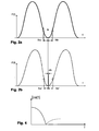
- the frequency of the zero point is then computed as (fka+fkb) / 2.
- the shape of the curve around the zero points may become asymmetrical. This is shown in Fig. 2 b. This in turn distorts the distance measurement.
- a possible design is thus that two parallel lines are fed by an input electrical strip set at the exact centre of the electrodes, yielding a perfect symmetry to the device whose response is totally independent of the direction of propagation of the light.
- Fig. 3a in a top view and Fig. 3b in a cross sectional view show such an integrated phase modulator with such symmetrical electrodes:
- a waveguide 22 is embedded, and an coplanar electrode pair 23 is arranged to apply a field to the waveguide 22.
- One electrode of the electrode pair 23 is fed by an input strip 24 or first contact section from, for example, a signal generator 26, the other electrode is connected by an output strip 25 or second contact section to, for example, a termination resistor arrangement 27.
- the electrodes 23 comprise a first branch 3a and a second branch 3b. These branches 3a, 3b both start at the first and second contact sections, i.e. at the input strip 24 and output strip 25 (both, for example, of microstrip type), but extend along the waveguide 22 in opposite directions.
- Each of the branches 3a, 3b comprises a first electrode section 11 connected at one end to the input strip 24 and running along the waveguide 22, and a second electrode section 12 connected at one end to the output strip 25 and running along the waveguide 22.
- the first and second electrode sections 11, 12 can be arranged symmetrically with regard to the waveguide 22.
- Each of the branches 3a, 3b ends at a corresponding branch endpoint 9a, 9b.
- the input strip 24 is electrically connected to and supplied by a signal generator 26, the output strip 25 is electrically connected to a termination element such as a resistor 27, whose impedance can be matched to the characteristic impedance of the electrodes.
- the input strip 24 and output strip 25 are located at a midpoint 16 along the length of the electrodes and are preferably symmetrically shaped and attached, each by a T-coupler 8, to the beginning of the first line sections 11 and the second line sections 12, respectively.
- the electrodes 23 give the electro-optic modulation response a low pass filter characteristic and consequently are not ideally suited to work at high frequencies (e.g. in the GHz range). This effect can be reduced to a limited degree by shortening the electrode length, but this in turn increases the required half wave voltage V ⁇ .
- An electrical signal on the electrode branches 3a, 3b generates an electrical field in the vicinity of the branches 3a, 3b.
- a section of the waveguide 22 in which this field affects the light passing along the waveguide 22 shall be called modulation region 17.
- Its length is essentially the length of the electrode along the waveguide 22, in other words, the sum of the extension of the first and second branch 3a, 3b.
- the electrical fields of the two sections 11, 12 are superposed, with the resulting superposed or total field affecting the modulation region 17.
- the first branch 3a influences the light in a first subregion 17a
- the second branch 3b influences the light in a second subregion 17b of the modulation region 17.
- the electrode length essentially equals the length of the modulation region 17, and the extension of each branch 3a, 3b equals the length of the corresponding subregion 17a, 17b.
- Fig. 3b shows a cross section along the XZ-plane of the integrated phase modulator of Fig. 3a .
- this figure schematically shows a bottom face 15 opposite the face carrying the electrode lines and having an inclined or wedged surface. This eliminates or at least reduces acoustical resonances that may be generated when the electrical signal is applied to the electrodes 23.
- Fig. 4 schematically shows the frequency response of the amplitude of the electro-optical phase modulation ⁇ (f):
- the amplitude of the phase modulation applied to the light wave propagating in the waveguide 22 follows a low pass function. That is, the amplitude has its maximal value at a frequency of zero, has lower values for nonzero frequencies, and falls monotonically up to a certain frequency, after which it can rise and fall again repeatedly, but only up to maximal values that decrease one after the other as the frequency increases.
- the frequency response can be simulated, given the geometry of the modulator and in particular of the electrodes. Conversely, given a particular requirement regarding the frequency response, such as a condition on the flatness of the response in a particular frequency range, it is straightforward to design the modulator and in particular the size of the electrodes.
- a distance measuring device utilising an integrated modulator as presented in the foregoing preferably has a structure and is operated like the distance measuring device of Fig. 1 , but with the bulk electro-optic crystal 103 replaced an integrated modulator 21, 22, 23 as described herein.
- the centre frequency of the microwave signal is, for example, in the range between 2 and 3 GHz.
- the modulation bandwidth is, for example, in the range of several hundreds of MHz. This is well suited for distance measurement applications.
Landscapes
- Engineering & Computer Science (AREA)
- Physics & Mathematics (AREA)
- General Physics & Mathematics (AREA)
- Computer Networks & Wireless Communication (AREA)
- Radar, Positioning & Navigation (AREA)
- Remote Sensing (AREA)
- Electromagnetism (AREA)
- Optical Radar Systems And Details Thereof (AREA)
- Optical Modulation, Optical Deflection, Nonlinear Optics, Optical Demodulation, Optical Logic Elements (AREA)
Abstract
A distance measuring device comprises a light source (101) emitting light, and such an electro-optic modulator (21, 22, 23) arranged such that the emitted light passes through the electro-optic modulator (21, 22, 23) in a first direction before being emitted from the distance measuring device, and after being reflected from a target passes through the electro-optic modulator (21, 22, 23) in a second direction which is opposite to the first direction. The forward electro-optic response of a modulating region (17) of the electro-optic modulator (21, 22, 23) is the same as the backward electro-optic response, and a centre of gravity of the modulation is independent of modulation frequency.
Description
- The invention relates to an electro-optic distance measuring device as described in the preamble of the corresponding independent claims.
- Relevant distance-measuring devices are known from
EP 0 205 406 ,EP 0 313 518 ,EP-A-1 647 838 ,WO 97/18486 EP patent application number 10 405 078 -
Fig. 1 schematically shows a distance measuring device for measuring absolute distance according to the prior art: Alight source 101 emits light, typically in the visible or infrared range, with centre wavelength λ, the spectral width Δλ of the source being broad enough in order to ensure a low coherence light emission. The parallel light beam emitted by thebroadband source 101 illuminates apolarising beam splitter 102, which ensures a linear polarization state for one of the transmitted beams. The polarized beam passes through an electro-optic crystal 103 havingelectrodes 104 on opposite sides. The incident light beam is polarized at 45° to the main axes of the electro-optic crystal 103, called slow (extraordinary) and fast (ordinary) axis, with different refractive indices ne > no, respectively. Two waves resulting from the projection on the orthogonal axes of the incident light field propagate in the electro-optic crystal 103 with a 90° polarization angle between them. Theelectrodes 104 allow to apply an electric field parallel to one of the main crystallographic axis of the electro-optic crystal 103. A sinusoidal electric signal with a frequency f is generated by asignal source 108 and applied to theelectrodes 104. This electric field generates a modification of the refractive index difference between the slow and the fast optical axes of the crystal. A phase modulation is thus introduced between the two orthogonal waves. The value of the index of modulation relative to the slow axis α s and to the fast axis αf depends on the electro-optic coefficient r of the for the crystal orientation considered, on the cube of the refractive index of the slow and fast axis respectively, on the distance gap between the electrodes, on the crystal length and on the optical wavelength, and on the voltage amplitude of the electrical signal. The polarization directions(s) along the path of the light indicated by small arrows. - At the output of the electro-
optic crystal 103, aquarter wave plate 105 is placed with its axes oriented at 45° with respect to the main axes of the electro-optic crystal 103. The light beam after passing through thequarter wave plate 105 passes on, along the distance to be measured, to reach a target. Acorner mirror 106 or other reflecting element is fixed to the target, reflecting the light back to the optical source. After passing a second time through thequarter wave 105 plate, the two orthogonal waves of the returning light are rotated by 90° and cross the electro-optic crystal 103 a second time, now in the opposite direction. The wave which was modulated the first time along the slow axis is now modulated along the fast axis, while the wave which was modulated along the fast axis the first time is now modulated along the slow axis. The modulation being experienced by the light is the same for the light passing in the forward and backward direction, but is a delayed by the time of flight of the wave on its way to the target and back. The returning light and part of the emitted light are then recombined at the second polarizer output port. The two resulting linear waves can now interfere. The resulting beam, modulated in amplitude according to the interference, is captured by aphotoreceiver 107. - Thus, basically, a light beam, from a laser or from a broadband light source, is generated, and guided by a focusing optical unit onto a polarizing beam splitter for linearly polarizing the light, and is subsequently guided onto a measurement path by an electro-optical modulator, a lambda/4 retarder and an exit optical unit. Light returning along the measurement path passes through the elements mentioned as far as the polarizing beam splitter and is guided onto a detector by the latter. An evaluation unit serves for determining the length of the measurement path on the basis of the detector signal.
- What is of relevance in the present context is that, in this method, outgoing and returning measurement light is modulated in a modulator. By variation of the frequency of said modulation, a minimum of the intensity of a detected measurement light beam is determined (or substantially synonymously, a zero-crossing of the derivative of the intensity). The length of the measurement path between the measurement device and a retroreflector or a semi-cooperative target is determined from the minimum frequency. A semi-cooperative target returns at least part of incident light along the direction of the incident light, e.g. by diffuse reflection.
- Current implementations of Fizeau-priciple based distance-measuring devices use electro-optic modulators with bulk crystals exhibiting the Pockels-effect. In order to reach the voltages of several 100 V (over a crystal width of ∼1mm) required for full modulation, the modulator needs an electrical drive-power of ∼1W, and the crystal is placed in a electrical resonator. Setting a particular modulation frequency requires mechanical tuning of the resonator, thus limiting the measurement rate (to e.g. 20 Hz).
- It is desirable to speed up the measurement by using an integrated optics modulator in a distance measurement device. However, since the measurement principle of the distance measurement device requires the light to pass the modulator twice, in opposing directions, known single pass modulators are not suitable.
- It is therefore an object of the invention to create a distance measuring device, using an integrated optics modulator which is traversed by both outgoing and returning light.
- A further object of the invention is to create a distance measuring device having an electro-optical modulator which can be operated with lower modulating voltages and with lower power consumption than known modulators.
- These objects are achieved by a distance measuring device according to claim 1.
- The electro-optic distance measuring device thus comprises an electro-optic modulator which in turn comprises a waveguide of a nonlinear optical material, and electrodes arranged to generate an electrical field in a modulating region of the waveguide when a voltage is applied to the electrodes, thereby modulating the phase of light passing through the waveguide. Therein
- ● the forward electro-optic response of the modulating region is the same as the backward electro-optic response (in other words: the effect, such as the phase shift, on light passing the modulator in one direction and light passing in the opposite direction is the same).
- In an embodiment, the electro-optic response in the used modulation frequency range has a flat (e.g. low-pass or band-pass) characteristic. In an embodiment, this means that over a bandwidth over 125 MHz the loss of electro-optic response is less than 25%, or that over a bandwidth over 125 MHz the electro-optic response varies by less than 25%.
- This allows the use of the modulator in an application in which two beams of light pass through the modulator in opposite directions and where it is important that the two beams be modulated with a high frequency, e.g. in the GHz range, in essentially the same manner.
- Note: A "band-pass characteristic" means, as is commonly known, that the electro-optic response is essentially zero when a DC voltage is applied to the electrode line, and with increasing frequency rises to a maximum and then falls again at least once. Similarly, a "low-pass characteristic" means that the electro-optic response is essentially at its maximum ("initial maximum") when a DC voltage is applied to the electrode line, and with increasing frequency falls continuously, either for all frequencies, or only up to a particular frequency, at which it reaches a minimum after which it rises again to a further maximum, usually to a level lower than the initial maximum, and falls again. This falling and rising may repeat itself for increasing frequencies, usually with decreasing height of the maxima.
- With such an integrated optics modulator with a very small waveguide and electrode separation, the field strength required for full modulation is thus reached with a modulation voltage of only a few Volts, resulting in a dramatic reduction of drive-power and no need for an external resonator and its time consuming mechanical tuning any more.
- In an embodiment, the centre of gravity of modulation is independent of modulation frequency. The centre of gravity of modulation is a point along the waveguide. Its location yCOG is defined as the integral, over the position along the waveguide, of the product of the phase modulation per unit length a with the position y, divided by the integral, over the position along the waveguide, of the phase modulation. That is

where y1 and y2 are the beginning and the end position of the modulation region along the waveguide axis Y. As a result, the centre of gravity of modulation divides the waveguide into two sections, with the total modulation of the light in both sections being the same (the total modulation in one section is the integral of the modulation along the section). - The distance measuring device comprises the electro-optic modulator. This allows the distance measuring device to perform at a high measurement rate with high accuracy and with low power consumption.
- In an embodiment, the distance measuring device comprises a light source emitting light, with the electro-optic modulator being arranged in the distance measuring device such that light emitted by the light source passes through the electro-optic modulator in a first direction before being emitted from the distance measuring device, and such emitted light after being reflected from a target outside the distance measuring device passes through the electro-optic modulator in a second direction which is opposite to the first direction.
- In an embodiment, the modulating region comprises a first subregion and a second subregion and the electrode line is capable to effect on light passing in one direction through the first subregion the same modulation as on light passing in the opposite direction through the second subregion.
- The superposition of the electrical fields from the two line sections affecting the modulation region results in the electrical field in the waveguide oscillating like a standing wave, symmetrical along the length of the lines, which in turn causes the symmetrical optical response.
- In an embodiment, the electrodes comprise a first branch and a second branch and a midpoint between the two branches, wherein the electrodes are able, when connected to an electric microwave signal source, to generate an electrical field distribution in the waveguide that is symmetrical with respect to the midpoint.
- As a result, light passing through the waveguide along the length of the modulating section in one direction experiences the same total phase shift (which is the integral of the time dependent and location dependent voltage induced phase shift along the modulating section) as light passing in the opposite direction at the same time. In other words, the forward electro-optic response is the same as the backward electro-optic response.
- Such a symmetrical configuration regarding the electrical properties of the branches allows to get the same electro-optic response in the forward and in the backward directions of propagation of light in the optical circuit. The symmetrical configuration regarding the electrical properties can be obtained by geometric symmetry of the branches.
- Thus, in an embodiment, the shape of the electrode line comprising the first and the second branch is symmetric with respect to the midpoint. The shape of the electrode line may be mirror-symmetric with respect to a plane passing through the midpoint and normal to the waveguide. Alternatively, the shape of the electrode line can have a rotational symmetry around an axis passing through the midpoint and normal to the plane in which the electrode line lies.
- In an embodiment, a bottom face of the substrate, opposed to the surface at which the waveguide and electrode line are arranged (top surface), is not parallel to the top surface, or in other words, the bottom face is inclined relative to the opposite, top surface (wedged shape). The substrate thus has the shape of part of a wedge. This reduces or eliminates acoustical resonances that may arise in the substrate due to the piezo-electrical effect.
- In summary, the electro-optic modulator comprises one or more of the following features:
- ● A birefringent electro-optic crystal.
- ● The ordinary and extraordinary axes are orthogonal to the direction of propagation of light.
- ● The direction of propagation of light is parallel to one of the ordinary axis
- ● The symmetrical configuration allows to get the same electro-optic response in the forward and in the backward directions of propagation of light in the optical circuit.
- The subject matter of the invention will be explained in more detail in the following text with reference to preferred exemplary embodiments which are illustrated in the attached drawings, which schematically show:
- Fig. 1
- the structure of an optical distance measuring device for measuring absolute distance;
- Fig. 2a, 2b
- the frequency dependence of a signal measured in the distance measuring device;
- Fig. 3a, 3b
- an integrated phase modulator with symmetrical electrodes; and
- Fig. 4
- the frequency response of the amplitude of the electro-optical phase modulation of the modulator of
Fig. 3 . - In principle, identical parts are provided with the same reference symbols in the Figures.
- Convention: A phase modulator uses an electro-optic crystal. The index of modulation will define the so-called half wave voltage Vπ. The half-wave voltage is a characteristic of an electro-optic modulator and corresponds to the voltage that needs to be applied to the crystal in order to modify the optical phase of transmitted light by π-radians.
- A guided wave configuration of an electro-optic modulator is as follows: a straight optical waveguide is shaped in a crystal surface, allowing the confinement of light in a small channel whose cross section is of some micrometers in width and height. Coplanar electrodes are arranged near the waveguides with a gap of some micrometers, allowing to apply a strong electric field to the waveguide. The half wave voltage can reduced to a few volts. much less than for bulk crystal modulators.
- Guided wave modulators in, e.g. lithium niobate, can work at very high frequencies, thanks to this low voltage configuration. Special travelling wave electrodes, made of coplanar waveguides (CPW) microwave lines allows to get a phase matching condition between the optical wave propagating in the waveguide and the microwave propagating in the CPW lines, both waves travelling in the same direction and a the same velocity. Generally, in a high speed travelling wave integrated optic modulator, the microwave electrical signal is fed by one side of the modulator to the input strip of the CPW line, close to the optical input of the waveguide. The end of the microwave line is set near the optical waveguide output.
- Using an integrated phase modulator in a distance meter arrangement as in
Fig. 1 , it can be shown that the shape of the average electrical power P(f) at the output of thephotoreceiver 107, as a function of modulation frequency, is similar to the curve shown inFig. 2a . The main property is that the zeros of P(f) remain in place. Ideally, the curves are symmetrical, which is a precondition for the distance measurement, which needs to determine a zero point of the curve. In one method for determining the zero point, rather than determining the zero point itself, two points to the left and right of the zero point having the same power P(fka)=P(fkb) are determined. The frequency of the zero point, assuming symmetry of the curves, is then computed as (fka+fkb)/2. However, depending on the geometrical and physical properties of the microwave electrodes, the shape of the curve around the zero points may become asymmetrical. This is shown inFig. 2 b. This in turn distorts the distance measurement. With the criterion P(fka)=P(fkb), the asymmetry can cause the resulting (fka+fkb)/2 to be different from the correct fk, introducing an error in the determination of the absolute distance L. - Furthermore, it is possible to demonstrate that if the electrodes are fed just by the middle of the electrode lines, P(f) becomes equal to zero, and a perfect symmetry of the response of the modulator is recovered for both the forward and backward directions of propagation of light. Furthermore, the centre of gravity of modulation remains at the same location, independent of the modulation frequency.
- A possible design is thus that two parallel lines are fed by an input electrical strip set at the exact centre of the electrodes, yielding a perfect symmetry to the device whose response is totally independent of the direction of propagation of the light.
-
Fig. 3a in a top view andFig. 3b in a cross sectional view show such an integrated phase modulator with such symmetrical electrodes: In asubstrate 21, awaveguide 22 is embedded, and ancoplanar electrode pair 23 is arranged to apply a field to thewaveguide 22. One electrode of theelectrode pair 23 is fed by an input strip 24 or first contact section from, for example, asignal generator 26, the other electrode is connected by an output strip 25 or second contact section to, for example, atermination resistor arrangement 27. - The
electrodes 23 comprise afirst branch 3a and asecond branch 3b. Thesebranches waveguide 22 in opposite directions. Each of thebranches first electrode section 11 connected at one end to the input strip 24 and running along thewaveguide 22, and asecond electrode section 12 connected at one end to the output strip 25 and running along thewaveguide 22. The first andsecond electrode sections waveguide 22. Each of thebranches corresponding branch endpoint signal generator 26, the output strip 25 is electrically connected to a termination element such as aresistor 27, whose impedance can be matched to the characteristic impedance of the electrodes. The input strip 24 and output strip 25 are located at amidpoint 16 along the length of the electrodes and are preferably symmetrically shaped and attached, each by a T-coupler 8, to the beginning of thefirst line sections 11 and thesecond line sections 12, respectively. - The
electrodes 23 give the electro-optic modulation response a low pass filter characteristic and consequently are not ideally suited to work at high frequencies (e.g. in the GHz range). This effect can be reduced to a limited degree by shortening the electrode length, but this in turn increases the required half wave voltage Vπ. - An electrical signal on the
electrode branches branches waveguide 22 in which this field affects the light passing along thewaveguide 22 shall be calledmodulation region 17. Its length is essentially the length of the electrode along thewaveguide 22, in other words, the sum of the extension of the first andsecond branch branch sections modulation region 17. Thefirst branch 3a influences the light in afirst subregion 17a, thesecond branch 3b influences the light in asecond subregion 17b of themodulation region 17. In the embodiment presented in the present application, the electrode length essentially equals the length of themodulation region 17, and the extension of eachbranch corresponding subregion -
Fig. 3b shows a cross section along the XZ-plane of the integrated phase modulator ofFig. 3a . In addition to the elements already described, this figure schematically shows abottom face 15 opposite the face carrying the electrode lines and having an inclined or wedged surface. This eliminates or at least reduces acoustical resonances that may be generated when the electrical signal is applied to theelectrodes 23. -
Fig. 4 schematically shows the frequency response of the amplitude of the electro-optical phase modulation Δφ(f): The amplitude of the phase modulation applied to the light wave propagating in thewaveguide 22 follows a low pass function. That is, the amplitude has its maximal value at a frequency of zero, has lower values for nonzero frequencies, and falls monotonically up to a certain frequency, after which it can rise and fall again repeatedly, but only up to maximal values that decrease one after the other as the frequency increases. The frequency response can be simulated, given the geometry of the modulator and in particular of the electrodes. Conversely, given a particular requirement regarding the frequency response, such as a condition on the flatness of the response in a particular frequency range, it is straightforward to design the modulator and in particular the size of the electrodes. - A distance measuring device utilising an integrated modulator as presented in the foregoing preferably has a structure and is operated like the distance measuring device of
Fig. 1 , but with the bulk electro-optic crystal 103 replaced anintegrated modulator - In an embodiment, the centre frequency of the microwave signal is, for example, in the range between 2 and 3 GHz. The modulation bandwidth is, for example, in the range of several hundreds of MHz. This is well suited for distance measurement applications.
- While the invention has been described in present embodiments, it is distinctly understood that the invention is not limited thereto, but may be otherwise variously embodied and practised within the scope of the claims. For example, whereas the embodiments shown so far use a single source connected to the input strip and a terminating resistance connected to the output, alternative embodiments can have a generalized impedance or a second source connected to the output.
Claims (13)
- An electro-optic distance measuring device comprising an electro-optic modulator, wherein the electro-optic modulator comprises a waveguide (22) of a nonlinear optical material and electrodes (23) arranged to generate an electrical field in a modulating region (17) of the waveguide (22) when a voltage is applied to the electrodes (23), and thereby to modulate the phase of light passing through the waveguide (22),
characterised in that● the forward electro-optic response of the modulating region (17) is the same as the backward electro-optic response. - The distance measuring device of claim 1, wherein the electro-optic response of the modulating region (17) has a flat characteristic.
- The distance measuring device of claim 1 or 2, wherein the electro-optic response of the modulating region (17) has a low-pass characteristic.
- The distance measuring device of claim 1 or 2, wherein the electro-optic response of the modulating region (17) has a band-pass characteristic.
- The distance measuring device of one of the preceding claims, comprising a light source (101) emitting light, the electro-optic modulator being arranged in the distance measuring device such that light emitted by the light source (101) passes through the electro-optic modulator in a first direction before being emitted from the distance measuring device, and such emitted light after being reflected from a target outside the distance measuring device passes through the electro-optic modulator in a second direction which is opposite to the first direction.
- The distance measuring device of one of the preceding claims, wherein a centre of gravity of the modulation is independent of modulation frequency.
- The distance measuring device of claim 6, wherein centre of gravity of modulation divides the waveguide into two sections, with the total modulation of the light in both sections being the same.
- The distance measuring device of one of the preceding claims, wherein● the modulating region (17) comprises a first subregion (17a) and a second subregion (17b) and the electrodes (23) are capable to effect on light passing in one direction through the first subregion (17a) the same modulation as on light passing in the opposite direction through the second subregion (17b).
- The distance measuring device of one of the preceding claims, wherein the electrodes (23) comprise a first branch (3a) and a second branch (3b) and a midpoint (16) between the two branches, wherein the electrodes (23) are able, when connected to an electric microwave signal source, to generate an electrical field distribution in the waveguide (22) that is symmetrical with respect to the midpoint (16).
- The distance measuring device of one of the preceding claims, wherein the shape of the electrodes (23) comprising the first and the second branch (3a, 3b) is symmetric with respect to the midpoint.
- The electro-optic modulator of claim 10, wherein the shape of the electrodes (23) is mirror-symmetric with respect to a plane passing through the midpoint and normal to the waveguide (22).
- The distance measuring device of claim 10, wherein the shape of the electrodes (23) has a rotational symmetry around an axis passing through the midpoint and normal to the plane in which the electrode line (3) lies.
- The distance measuring device of one of the preceding claims, in which a bottom face (15) of the substrate (1), opposed to the surface at which the waveguide (22) and electrode line (3) are arranged, is wedged, that is, inclined relative to the opposite surface.
Priority Applications (6)
| Application Number | Priority Date | Filing Date | Title |
|---|---|---|---|
| EP12405038.6A EP2653884A1 (en) | 2012-04-16 | 2012-04-16 | Electro-optic distance-measuring device |
| US14/394,217 US9405007B2 (en) | 2012-04-16 | 2013-03-06 | Electro-optic distance-measuring device |
| EP13709735.8A EP2839314B1 (en) | 2012-04-16 | 2013-03-06 | Electro-optic distance-measuring device |
| JP2015506058A JP6017018B2 (en) | 2012-04-16 | 2013-03-06 | Electro-optic distance measuring device |
| PCT/CH2013/000037 WO2013155637A1 (en) | 2012-04-16 | 2013-03-06 | Electro-optic distance-measuring device |
| CN201380020023.2A CN104204843B (en) | 2012-04-16 | 2013-03-06 | Electro-optic distance-measuring device |
Applications Claiming Priority (1)
| Application Number | Priority Date | Filing Date | Title |
|---|---|---|---|
| EP12405038.6A EP2653884A1 (en) | 2012-04-16 | 2012-04-16 | Electro-optic distance-measuring device |
Publications (1)
| Publication Number | Publication Date |
|---|---|
| EP2653884A1 true EP2653884A1 (en) | 2013-10-23 |
Family
ID=47891323
Family Applications (2)
| Application Number | Title | Priority Date | Filing Date |
|---|---|---|---|
| EP12405038.6A Withdrawn EP2653884A1 (en) | 2012-04-16 | 2012-04-16 | Electro-optic distance-measuring device |
| EP13709735.8A Active EP2839314B1 (en) | 2012-04-16 | 2013-03-06 | Electro-optic distance-measuring device |
Family Applications After (1)
| Application Number | Title | Priority Date | Filing Date |
|---|---|---|---|
| EP13709735.8A Active EP2839314B1 (en) | 2012-04-16 | 2013-03-06 | Electro-optic distance-measuring device |
Country Status (5)
| Country | Link |
|---|---|
| US (1) | US9405007B2 (en) |
| EP (2) | EP2653884A1 (en) |
| JP (1) | JP6017018B2 (en) |
| CN (1) | CN104204843B (en) |
| WO (1) | WO2013155637A1 (en) |
Cited By (2)
| Publication number | Priority date | Publication date | Assignee | Title |
|---|---|---|---|---|
| EP3388861A1 (en) * | 2017-04-11 | 2018-10-17 | Leica Geosystems AG | Absolute measurement of distance to dynamic targets |
| GB2585437A (en) * | 2019-04-12 | 2021-01-13 | Amazon Tech Inc | Energy efficient, high resolution light detection and ranging imaging receiver with large field-of-view |
Families Citing this family (9)
| Publication number | Priority date | Publication date | Assignee | Title |
|---|---|---|---|---|
| EP2653908A1 (en) | 2012-04-16 | 2013-10-23 | Leica Geosystems AG | Electro-optic modulator and electro-optic distance-measuring device |
| US10578482B2 (en) * | 2013-10-23 | 2020-03-03 | Pixart Imaging Incorporation | Proximity sensing device and light guiding method thereof |
| US10107762B2 (en) * | 2015-01-30 | 2018-10-23 | Hitachi High-Technologies Corporation | Examination device |
| JP6833449B2 (en) * | 2016-10-27 | 2021-02-24 | パイオニア株式会社 | Measuring device and measuring method |
| EP3401634A1 (en) * | 2017-05-12 | 2018-11-14 | Taylor Hobson Limited | Distance measuring assembly for determining the distance to an object |
| WO2019167151A1 (en) | 2018-02-28 | 2019-09-06 | 株式会社日立ハイテクノロジーズ | Inspection device and inspection method for same |
| GB2578583B (en) * | 2018-10-30 | 2020-11-18 | Rockley Photonics Ltd | Optoelectronic modulator, photonic integrated circuit, and method |
| CN112180390B (en) * | 2020-09-18 | 2022-05-06 | 常州大学 | A distance measuring device and method |
| CN112505653A (en) * | 2020-11-23 | 2021-03-16 | 杭州蓝芯科技有限公司 | Light source, depth camera and laser radar based on electro-optical modulation |
Citations (4)
| Publication number | Priority date | Publication date | Assignee | Title |
|---|---|---|---|---|
| US3424531A (en) * | 1965-09-17 | 1969-01-28 | Commerce Usa | Distance measuring instrument using a pair of modulated light waves |
| EP0313518A2 (en) * | 1987-10-23 | 1989-04-26 | Leica AG | Method for electrooptical distance measurement |
| US5764360A (en) * | 1995-11-15 | 1998-06-09 | Leica Ag | Electro-optical measuring device for absolute distances |
| EP2381269A1 (en) * | 2010-04-13 | 2011-10-26 | Leica Geosystems AG | Coordinate measuring device with automated targeting |
Family Cites Families (17)
| Publication number | Priority date | Publication date | Assignee | Title |
|---|---|---|---|---|
| US4606638A (en) | 1983-11-03 | 1986-08-19 | Zygo Corporation | Distance measuring interferometer and method of use |
| US4979178A (en) | 1989-06-20 | 1990-12-18 | The Boeing Company | Tunable narrow-linewidth semiconductor laser |
| US5208697A (en) * | 1990-03-30 | 1993-05-04 | Hughes Aircraft Company | Microwave frequency range electro-optic modulator with efficient input coupling and smooth wideband frequency response |
| JP3359943B2 (en) | 1992-11-16 | 2002-12-24 | 日本碍子株式会社 | Light modulator |
| JP2821349B2 (en) | 1993-11-05 | 1998-11-05 | 住友大阪セメント株式会社 | Optical waveguide device |
| JP3654992B2 (en) | 1996-02-23 | 2005-06-02 | 富士通株式会社 | Light control element |
| JP3854656B2 (en) * | 1996-03-01 | 2006-12-06 | 住友大阪セメント株式会社 | Light intensity modulator and light wave distance meter |
| JP3088988B2 (en) | 1997-12-24 | 2000-09-18 | 住友大阪セメント株式会社 | Traveling wave optical modulator and optical modulation method |
| US6483953B1 (en) | 1999-05-11 | 2002-11-19 | Jds Uniphase Corporation | External optical modulation using non-co-linear compensation networks |
| JP3902047B2 (en) | 2002-03-29 | 2007-04-04 | 独立行政法人科学技術振興機構 | Waveguide type optical modulator |
| EP1444482B1 (en) | 2001-11-16 | 2010-05-26 | Zygo Corporation | Scanning interferometer for aspheric surfaces and wavefronts |
| JP4096823B2 (en) | 2003-06-18 | 2008-06-04 | 三菱電機株式会社 | Laser equipment |
| EP1647838B1 (en) | 2004-10-13 | 2010-04-28 | Leica Geosystems AG | Method and apparatus for absolute distance measurement |
| EP2245482B1 (en) | 2008-02-19 | 2018-12-26 | Leica Geosystems AG | Electro-optical distance-measuring unit |
| US8483523B2 (en) * | 2009-09-14 | 2013-07-09 | Ricoh Company, Ltd. | Optical waveguide electro-optic device and process of manufacturing optical waveguide electro-optic device |
| JP4991910B2 (en) | 2010-05-31 | 2012-08-08 | 住友大阪セメント株式会社 | Light control element |
| EP2653908A1 (en) | 2012-04-16 | 2013-10-23 | Leica Geosystems AG | Electro-optic modulator and electro-optic distance-measuring device |
-
2012
- 2012-04-16 EP EP12405038.6A patent/EP2653884A1/en not_active Withdrawn
-
2013
- 2013-03-06 US US14/394,217 patent/US9405007B2/en active Active
- 2013-03-06 WO PCT/CH2013/000037 patent/WO2013155637A1/en active Application Filing
- 2013-03-06 JP JP2015506058A patent/JP6017018B2/en not_active Expired - Fee Related
- 2013-03-06 CN CN201380020023.2A patent/CN104204843B/en active Active
- 2013-03-06 EP EP13709735.8A patent/EP2839314B1/en active Active
Patent Citations (4)
| Publication number | Priority date | Publication date | Assignee | Title |
|---|---|---|---|---|
| US3424531A (en) * | 1965-09-17 | 1969-01-28 | Commerce Usa | Distance measuring instrument using a pair of modulated light waves |
| EP0313518A2 (en) * | 1987-10-23 | 1989-04-26 | Leica AG | Method for electrooptical distance measurement |
| US5764360A (en) * | 1995-11-15 | 1998-06-09 | Leica Ag | Electro-optical measuring device for absolute distances |
| EP2381269A1 (en) * | 2010-04-13 | 2011-10-26 | Leica Geosystems AG | Coordinate measuring device with automated targeting |
Cited By (7)
| Publication number | Priority date | Publication date | Assignee | Title |
|---|---|---|---|---|
| EP3388861A1 (en) * | 2017-04-11 | 2018-10-17 | Leica Geosystems AG | Absolute measurement of distance to dynamic targets |
| CN108761478A (en) * | 2017-04-11 | 2018-11-06 | 莱卡地球系统公开股份有限公司 | For the absolute distance measurement of dynamic object |
| US10775503B2 (en) | 2017-04-11 | 2020-09-15 | Leica Geosystems Ag | Absolute distance measurement to dynamic targets |
| CN108761478B (en) * | 2017-04-11 | 2022-10-25 | 莱卡地球系统公开股份有限公司 | Absolute distance measurement for dynamic targets |
| GB2585437A (en) * | 2019-04-12 | 2021-01-13 | Amazon Tech Inc | Energy efficient, high resolution light detection and ranging imaging receiver with large field-of-view |
| GB2585437B (en) * | 2019-04-12 | 2023-05-24 | Amazon Tech Inc | Energy efficient, high resolution light detection and ranging imaging receiver with large field-of-view |
| US11822157B2 (en) | 2019-04-12 | 2023-11-21 | Amazon Technologies, Inc. | Energy efficient, high resolution light detection and ranging imaging receiver with large field-of-view |
Also Published As
| Publication number | Publication date |
|---|---|
| US9405007B2 (en) | 2016-08-02 |
| JP2015519547A (en) | 2015-07-09 |
| WO2013155637A1 (en) | 2013-10-24 |
| EP2839314B1 (en) | 2021-10-06 |
| CN104204843A (en) | 2014-12-10 |
| EP2839314A1 (en) | 2015-02-25 |
| CN104204843B (en) | 2017-04-26 |
| US20150077758A1 (en) | 2015-03-19 |
| JP6017018B2 (en) | 2016-10-26 |
Similar Documents
| Publication | Publication Date | Title |
|---|---|---|
| EP2839314B1 (en) | Electro-optic distance-measuring device | |
| EP2839334B1 (en) | Electro-optic modulator and electro-optic distance-measuring device | |
| EP1411387B1 (en) | Optical frequency comb- generator | |
| JP2619981B2 (en) | Electromagnetic field strength measuring device | |
| US20170248807A1 (en) | Electro-optical phase modulation system | |
| US6285182B1 (en) | Electro-optic voltage sensor | |
| CA2711541C (en) | Electro-optical distance-measuring unit | |
| EP0699925B1 (en) | Optical type displacement detecting apparatus | |
| US5629793A (en) | Frequency shifter and optical displacement measurement apparatus using the same | |
| JPH03102264A (en) | Electric signal sampling system using microwave optical pulse | |
| KR20170141148A (en) | Voltage Sensor System | |
| US10670520B2 (en) | Optical analysis device and optical analysis method | |
| JP2004525361A (en) | Method for electro-optically measuring voltage in a temperature-compensated manner and apparatus for carrying out the method | |
| US20220404274A1 (en) | Spectroscopic measurement device | |
| EP0357475A1 (en) | Electro-optical measuring system for the frequency analysis of very wide band signals | |
| Porte et al. | Band pass & low-voltage symmetrical electro-optic modulator for absolute distance metrology | |
| JP7336951B2 (en) | Voltage measuring device and voltage measuring method | |
| JP2023183122A (en) | voltage measuring device | |
| RU20586U1 (en) | DEVICE FOR MEASURING MODULE AND PHASE OF REFLECTING RATIO | |
| RU151737U1 (en) | DEVICE FOR DETERMINING MICROWAVE RADIATION PARAMETERS | |
| US20020109901A1 (en) | Hybrid methods and apparatus for polarization transformation | |
| Zhao et al. | Laser ranging based on electro-optic switch | |
| JPH07181213A (en) | Electro-optical electric field measuring device | |
| Zhao et al. | Laser ranging based on electro-optic effect in crystal | |
| Siahmakoun et al. | Double-and single-sideband suppressed-carrier optical modulator implemented at 1320 nm using LiNbO3 crystals and bulk optics |
Legal Events
| Date | Code | Title | Description |
|---|---|---|---|
| PUAI | Public reference made under article 153(3) epc to a published international application that has entered the european phase |
Free format text: ORIGINAL CODE: 0009012 |
|
| AK | Designated contracting states |
Kind code of ref document: A1 Designated state(s): AL AT BE BG CH CY CZ DE DK EE ES FI FR GB GR HR HU IE IS IT LI LT LU LV MC MK MT NL NO PL PT RO RS SE SI SK SM TR |
|
| AX | Request for extension of the european patent |
Extension state: BA ME |
|
| STAA | Information on the status of an ep patent application or granted ep patent |
Free format text: STATUS: THE APPLICATION IS DEEMED TO BE WITHDRAWN |
|
| 18D | Application deemed to be withdrawn |
Effective date: 20140424 |