WO2016121597A1 - フェナントロリン誘導体、それを含有する電子デバイス、発光素子および光電変換素子 - Google Patents
フェナントロリン誘導体、それを含有する電子デバイス、発光素子および光電変換素子 Download PDFInfo
- Publication number
- WO2016121597A1 WO2016121597A1 PCT/JP2016/051578 JP2016051578W WO2016121597A1 WO 2016121597 A1 WO2016121597 A1 WO 2016121597A1 JP 2016051578 W JP2016051578 W JP 2016051578W WO 2016121597 A1 WO2016121597 A1 WO 2016121597A1
- Authority
- WO
- WIPO (PCT)
- Prior art keywords
- group
- layer
- light emitting
- phenanthroline derivative
- electron
- Prior art date
- Legal status (The legal status is an assumption and is not a legal conclusion. Google has not performed a legal analysis and makes no representation as to the accuracy of the status listed.)
- Ceased
Links
- 0 *c1c(*)c(c(*)c(*)c(c2n3)c(*)c(*)c3I)c2nc1* Chemical compound *c1c(*)c(c(*)c(*)c(c2n3)c(*)c(*)c3I)c2nc1* 0.000 description 3
- OFOSAXOSYPMDFN-UHFFFAOYSA-N C(CC(c(ccc1ccc2cc3)nc1c2nc3-c1cc2ccccc2c2ccccc12)=C1)C=C1c1ncccc1 Chemical compound C(CC(c(ccc1ccc2cc3)nc1c2nc3-c1cc2ccccc2c2ccccc12)=C1)C=C1c1ncccc1 OFOSAXOSYPMDFN-UHFFFAOYSA-N 0.000 description 1
- IOKDVJLMGGILBQ-UHFFFAOYSA-N C1c2cccc(cc3)c2c2c3c(-c(ccc3ccc4cc5)nc3c4nc5-c(cc3)ccc3-c3cccnc3)ccc2C1 Chemical compound C1c2cccc(cc3)c2c2c3c(-c(ccc3ccc4cc5)nc3c4nc5-c(cc3)ccc3-c3cccnc3)ccc2C1 IOKDVJLMGGILBQ-UHFFFAOYSA-N 0.000 description 1
- VEKGGELLMXIBER-UHFFFAOYSA-N CC(C)(C)c1cc(cc2)c3c4c2c(-c(cc2)ccc2-c2ncccc2)cc(-c(cc2)ccc2-c(ccc2ccc5cc6)nc2c5nc6-c2cnc(cccc5)c5c2)c4ccc3c1 Chemical compound CC(C)(C)c1cc(cc2)c3c4c2c(-c(cc2)ccc2-c2ncccc2)cc(-c(cc2)ccc2-c(ccc2ccc5cc6)nc2c5nc6-c2cnc(cccc5)c5c2)c4ccc3c1 VEKGGELLMXIBER-UHFFFAOYSA-N 0.000 description 1
- UTXWCJHTMDJDTC-UHFFFAOYSA-N CC(C)(C)c1cc(cc2)c3c4c2c(-c2cc(cccc5)c5cc2)cc(-c(ccc2ccc5cc6)nc2c5nc6-c2cnc(cccc5)c5c2)c4ccc3c1 Chemical compound CC(C)(C)c1cc(cc2)c3c4c2c(-c2cc(cccc5)c5cc2)cc(-c(ccc2ccc5cc6)nc2c5nc6-c2cnc(cccc5)c5c2)c4ccc3c1 UTXWCJHTMDJDTC-UHFFFAOYSA-N 0.000 description 1
- WIZSIAWQQIJKNK-UHFFFAOYSA-N CC(C)(c1c2)c3cc(-c(cc4cc5)c(ccc(-c6cc7cc(cccc8)c8nc7cc6)n6)c6c4nc5-c4cc(-c5ccc(-c6cccc7c6c-6ccc7)c-6c5)ccc4)ccc3-c1ccc2-c(cc1)ccc1-c(ccc1ccc2cc3)nc1c2nc3-c1cc2cc(cccc3)c3nc2cc1 Chemical compound CC(C)(c1c2)c3cc(-c(cc4cc5)c(ccc(-c6cc7cc(cccc8)c8nc7cc6)n6)c6c4nc5-c4cc(-c5ccc(-c6cccc7c6c-6ccc7)c-6c5)ccc4)ccc3-c1ccc2-c(cc1)ccc1-c(ccc1ccc2cc3)nc1c2nc3-c1cc2cc(cccc3)c3nc2cc1 WIZSIAWQQIJKNK-UHFFFAOYSA-N 0.000 description 1
- FZUFUBHDVZOGOX-UHFFFAOYSA-N CC(C)(c1c2)c3cc(-c(ccc4ccc5cc6)nc4c5nc6-c(cc4)ccc4-c4cnccn4)ccc3-c1ccc2-c(cc1cc2)c(ccc(-c(cc3)cc-4c3-c3cccc5c3c-4ccc5)n3)c3c1nc2-c1cccc(-c2cnccn2)c1 Chemical compound CC(C)(c1c2)c3cc(-c(ccc4ccc5cc6)nc4c5nc6-c(cc4)ccc4-c4cnccn4)ccc3-c1ccc2-c(cc1cc2)c(ccc(-c(cc3)cc-4c3-c3cccc5c3c-4ccc5)n3)c3c1nc2-c1cccc(-c2cnccn2)c1 FZUFUBHDVZOGOX-UHFFFAOYSA-N 0.000 description 1
- IZQSNHQSLFUOMD-UHFFFAOYSA-N CC1(C)c(cc(cc2)-c3nc(c4c(cc5)ccc(-c6cccc(-c7ccccn7)c6)n4)c5cc3)c2-c2c1cccc2 Chemical compound CC1(C)c(cc(cc2)-c3nc(c4c(cc5)ccc(-c6cccc(-c7ccccn7)c6)n4)c5cc3)c2-c2c1cccc2 IZQSNHQSLFUOMD-UHFFFAOYSA-N 0.000 description 1
- UIVPJKYDSWUBSR-UHFFFAOYSA-N CC1(C)c(cc(cc2)-c3nc(c4c(cc5)ccc(-c6cccc(-c7nc8ccccc8c(-c(cc8)ccc8-c8cccnc8)n7)c6)n4)c5cc3)c2-c2c1cccc2 Chemical compound CC1(C)c(cc(cc2)-c3nc(c4c(cc5)ccc(-c6cccc(-c7nc8ccccc8c(-c(cc8)ccc8-c8cccnc8)n7)c6)n4)c5cc3)c2-c2c1cccc2 UIVPJKYDSWUBSR-UHFFFAOYSA-N 0.000 description 1
- QOSQFMAHXZMJEV-UHFFFAOYSA-N CC1(C)c2cc(-c(cc3)ccc3-c(ccc3ccc4cc5)nc3c4nc5-c3cccc(-c4cncc(-c5ccccc5)n4)c3)ccc2-c2ccccc12 Chemical compound CC1(C)c2cc(-c(cc3)ccc3-c(ccc3ccc4cc5)nc3c4nc5-c3cccc(-c4cncc(-c5ccccc5)n4)c3)ccc2-c2ccccc12 QOSQFMAHXZMJEV-UHFFFAOYSA-N 0.000 description 1
- YSTDVNDYHNVNPV-UHFFFAOYSA-N CC1(C)c2cc(-c(ccc3ccc4cc5)nc3c4nc5-c(cc3)ccc3-c(nc3)cnc3-c3ccncc3)ccc2-c2c1cccc2 Chemical compound CC1(C)c2cc(-c(ccc3ccc4cc5)nc3c4nc5-c(cc3)ccc3-c(nc3)cnc3-c3ccncc3)ccc2-c2c1cccc2 YSTDVNDYHNVNPV-UHFFFAOYSA-N 0.000 description 1
- LIUJHTSXMIWQCY-UHFFFAOYSA-N CC1(C)c2cc(-c(ccc3ccc4cc5)nc3c4nc5-c3cc(-c(cc4)cc5c4nc(-c4cc(cccc6)c6cc4)nc5-c4ccccc4)ccc3)ccc2-c2ccccc12 Chemical compound CC1(C)c2cc(-c(ccc3ccc4cc5)nc3c4nc5-c3cc(-c(cc4)cc5c4nc(-c4cc(cccc6)c6cc4)nc5-c4ccccc4)ccc3)ccc2-c2ccccc12 LIUJHTSXMIWQCY-UHFFFAOYSA-N 0.000 description 1
- UUCDGKHBLDZADX-UHFFFAOYSA-N CC1(C)c2cc(-c3cccc(-c(ccc4ccc5cc6)nc4c5nc6-c4cccc(-c(nc5)ncc5-c5cc(nccc6)c6cc5)c4)c3)ccc2-c2c1cccc2 Chemical compound CC1(C)c2cc(-c3cccc(-c(ccc4ccc5cc6)nc4c5nc6-c4cccc(-c(nc5)ncc5-c5cc(nccc6)c6cc5)c4)c3)ccc2-c2c1cccc2 UUCDGKHBLDZADX-UHFFFAOYSA-N 0.000 description 1
- NKYAQYMUTKXKRO-UHFFFAOYSA-N CC1(C)c2cc(-c3cccc(-c4nc(c5nc(-c6cccc(-c(nc7)ncc7-c7c(cccc8)c8ccc7)c6)ccc5cc5)c5cc4)c3)ccc2-c2ccccc12 Chemical compound CC1(C)c2cc(-c3cccc(-c4nc(c5nc(-c6cccc(-c(nc7)ncc7-c7c(cccc8)c8ccc7)c6)ccc5cc5)c5cc4)c3)ccc2-c2ccccc12 NKYAQYMUTKXKRO-UHFFFAOYSA-N 0.000 description 1
- FQENSEPPJNDPEI-UHFFFAOYSA-N CC1(C)c2cc(-c3nc(c4nc(-c5cccc(-c6ccncc6)c5)ccc4cc4)c4cc3)ccc2-c2c1cccc2 Chemical compound CC1(C)c2cc(-c3nc(c4nc(-c5cccc(-c6ccncc6)c5)ccc4cc4)c4cc3)ccc2-c2c1cccc2 FQENSEPPJNDPEI-UHFFFAOYSA-N 0.000 description 1
- UZYRZRRAKDSRGI-UHFFFAOYSA-N c(cc1)cc(-c2cccc3c22)c1-c2ccc3-c(ccc1ccc2cc3)nc1c2nc3-c(cc1)ccc1-c1cccnc1 Chemical compound c(cc1)cc(-c2cccc3c22)c1-c2ccc3-c(ccc1ccc2cc3)nc1c2nc3-c(cc1)ccc1-c1cccnc1 UZYRZRRAKDSRGI-UHFFFAOYSA-N 0.000 description 1
- YQORHLCHGGAYLC-UHFFFAOYSA-N c(cc1)cc(-c2cccc3c22)c1-c2ccc3-c(ccc1ccc2cc3)nc1c2nc3-c(cc1)ccc1-c1cnccn1 Chemical compound c(cc1)cc(-c2cccc3c22)c1-c2ccc3-c(ccc1ccc2cc3)nc1c2nc3-c(cc1)ccc1-c1cnccn1 YQORHLCHGGAYLC-UHFFFAOYSA-N 0.000 description 1
- CHFXVSNDMLFFIJ-UHFFFAOYSA-N c(cc1)cc(c(cccc2)c2c2c3)c1c2ccc3-c(cc1)ccc1-c(ccc1ccc2cc3)nc1c2nc3-c1cccc(-c(nc2)cnc2-c2ccncc2)c1 Chemical compound c(cc1)cc(c(cccc2)c2c2c3)c1c2ccc3-c(cc1)ccc1-c(ccc1ccc2cc3)nc1c2nc3-c1cccc(-c(nc2)cnc2-c2ccncc2)c1 CHFXVSNDMLFFIJ-UHFFFAOYSA-N 0.000 description 1
- YFNQXAVCAIEZLQ-UHFFFAOYSA-N c(cc1)cc(c(cccc2)c2c2c3)c1c2ccc3-c(ccc1ccc2cc3)nc1c2nc3-c(cc1)ccc1-c1cnccn1 Chemical compound c(cc1)cc(c(cccc2)c2c2c3)c1c2ccc3-c(ccc1ccc2cc3)nc1c2nc3-c(cc1)ccc1-c1cnccn1 YFNQXAVCAIEZLQ-UHFFFAOYSA-N 0.000 description 1
- GUEHIBPIZQMZCE-UHFFFAOYSA-N c(cc1)cc(c2ccccc2c2c3)c1c2ccc3-c(ccc1ccc2cc3)nc1c2nc3-c(cc1)ccc1-c1ccccn1 Chemical compound c(cc1)cc(c2ccccc2c2c3)c1c2ccc3-c(ccc1ccc2cc3)nc1c2nc3-c(cc1)ccc1-c1ccccn1 GUEHIBPIZQMZCE-UHFFFAOYSA-N 0.000 description 1
- APSNIWIPGLBELG-UHFFFAOYSA-N c(cc1)cc(c2ccccc2c2c3)c1c2ccc3-c1nc(c2c(cc3)ccc(-c(cc4)ccc4-c4cccnc4)n2)c3cc1 Chemical compound c(cc1)cc(c2ccccc2c2c3)c1c2ccc3-c1nc(c2c(cc3)ccc(-c(cc4)ccc4-c4cccnc4)n2)c3cc1 APSNIWIPGLBELG-UHFFFAOYSA-N 0.000 description 1
- LOCJIMTVNLGXSJ-UHFFFAOYSA-N c(cc1)cc(cc2)c1cc2-c1cccc(-c2nc(c3nc(-c(cc4)ccc4-c(nc4)ncc4-c4c(cccn5)c5ccc4)ccc3cc3)c3cc2)c1 Chemical compound c(cc1)cc(cc2)c1cc2-c1cccc(-c2nc(c3nc(-c(cc4)ccc4-c(nc4)ncc4-c4c(cccn5)c5ccc4)ccc3cc3)c3cc2)c1 LOCJIMTVNLGXSJ-UHFFFAOYSA-N 0.000 description 1
- NCNNDJYKDNSEPE-UHFFFAOYSA-N c(cc1)cc(cc2)c1cc2-c1nc(-c(cc2)ccc2-c(ccc2ccc3cc4)nc2c3nc4-c2cc(-c3c(cccc4)c4c(cccc4)c4c3)ccc2)cnc1 Chemical compound c(cc1)cc(cc2)c1cc2-c1nc(-c(cc2)ccc2-c(ccc2ccc3cc4)nc2c3nc4-c2cc(-c3c(cccc4)c4c(cccc4)c4c3)ccc2)cnc1 NCNNDJYKDNSEPE-UHFFFAOYSA-N 0.000 description 1
- XVFKVPIBFAFIMC-UHFFFAOYSA-N c(cc1)cc(cc2)c1cc2-c1nc(-c(cc2)ccc2-c(ccc2ccc3cc4)nc2c3nc4-c2ccc(c(cccc3)c3c3c4cccc3)c4c2)nc2c1cccc2 Chemical compound c(cc1)cc(cc2)c1cc2-c1nc(-c(cc2)ccc2-c(ccc2ccc3cc4)nc2c3nc4-c2ccc(c(cccc3)c3c3c4cccc3)c4c2)nc2c1cccc2 XVFKVPIBFAFIMC-UHFFFAOYSA-N 0.000 description 1
- ZVLDAZUIKYEXQQ-UHFFFAOYSA-N c(cc1)cc(cc2)c1cc2-c1nc(c2c(cc3)ccc(-c4cc(-c5cncc(-c6cc(cccc7)c7nc6)n5)ccc4)n2)c3cc1 Chemical compound c(cc1)cc(cc2)c1cc2-c1nc(c2c(cc3)ccc(-c4cc(-c5cncc(-c6cc(cccc7)c7nc6)n5)ccc4)n2)c3cc1 ZVLDAZUIKYEXQQ-UHFFFAOYSA-N 0.000 description 1
- SMWPDYJISXWVLJ-UHFFFAOYSA-N c(cc1)cc-2c1-c1ccc(-c3cc(-c(ccc4ccc5cc6)nc4c5nc6-c4cccc(-c5cncc(-c6cc7ccccc7nc6)n5)c4)ccc3)c3c1c-2ccc3 Chemical compound c(cc1)cc-2c1-c1ccc(-c3cc(-c(ccc4ccc5cc6)nc4c5nc6-c4cccc(-c5cncc(-c6cc7ccccc7nc6)n5)c4)ccc3)c3c1c-2ccc3 SMWPDYJISXWVLJ-UHFFFAOYSA-N 0.000 description 1
- JSFVGYJAOXVMHQ-UHFFFAOYSA-N c(cc1)cc-2c1-c1ccc(-c3cccc(-c(ccc4ccc5cc6)nc4c5nc6-c(cc4)ccc4-c(nc4)ncc4-c4cccnc4)c3)c3cccc-2c13 Chemical compound c(cc1)cc-2c1-c1ccc(-c3cccc(-c(ccc4ccc5cc6)nc4c5nc6-c(cc4)ccc4-c(nc4)ncc4-c4cccnc4)c3)c3cccc-2c13 JSFVGYJAOXVMHQ-UHFFFAOYSA-N 0.000 description 1
- DKMLYHHMNRCUKF-UHFFFAOYSA-N c(cc1)cc2c1c(-c(cc1)ccc1-c(ccc1ccc3cc4)nc1c3nc4-c1cc(-c(cc3)c(cc4)c5c3ccc3c5c4ccc3-c3cccnc3)ccc1)cnc2 Chemical compound c(cc1)cc2c1c(-c(cc1)ccc1-c(ccc1ccc3cc4)nc1c3nc4-c1cc(-c(cc3)c(cc4)c5c3ccc3c5c4ccc3-c3cccnc3)ccc1)cnc2 DKMLYHHMNRCUKF-UHFFFAOYSA-N 0.000 description 1
- NFHVDICWTKIFAE-UHFFFAOYSA-N c(cc1)cc2c1c(-c(cc1)ccc1-c(ccc1ccc3cc4)nc1c3nc4-c1cc3cc(cccc4)c4nc3cc1)ccc2 Chemical compound c(cc1)cc2c1c(-c(cc1)ccc1-c(ccc1ccc3cc4)nc1c3nc4-c1cc3cc(cccc4)c4nc3cc1)ccc2 NFHVDICWTKIFAE-UHFFFAOYSA-N 0.000 description 1
- HEYRYLLCJVFEMI-UHFFFAOYSA-N c(cc1)cc2c1c(ccc(-c(cc1)ccc1-c(ccc1ccc3cc4)nc1c3nc4-c1cccc(-c(nc3)ncc3-c3cccnc3)c1)c1)c1c1ccccc21 Chemical compound c(cc1)cc2c1c(ccc(-c(cc1)ccc1-c(ccc1ccc3cc4)nc1c3nc4-c1cccc(-c(nc3)ncc3-c3cccnc3)c1)c1)c1c1ccccc21 HEYRYLLCJVFEMI-UHFFFAOYSA-N 0.000 description 1
- MSXSXMDBTDDOJP-UHFFFAOYSA-N c(cc1)cc2c1c(cccc1)c1c(-c(ccc1ccc3cc4)nc1c3nc4-c(cc1)ccc1-c1nc(cccc3)c3c(-c3cccnc3)n1)c2 Chemical compound c(cc1)cc2c1c(cccc1)c1c(-c(ccc1ccc3cc4)nc1c3nc4-c(cc1)ccc1-c1nc(cccc3)c3c(-c3cccnc3)n1)c2 MSXSXMDBTDDOJP-UHFFFAOYSA-N 0.000 description 1
- YCJHMEIDKWTIHV-UHFFFAOYSA-N c(cc1)cc2c1c(cccc1)c1c(-c1cccc(-c(ccc3ccc4cc5)nc3c4nc5-c3cc4cc(cccc5)c5nc4cc3)c1)c2 Chemical compound c(cc1)cc2c1c(cccc1)c1c(-c1cccc(-c(ccc3ccc4cc5)nc3c4nc5-c3cc4cc(cccc5)c5nc4cc3)c1)c2 YCJHMEIDKWTIHV-UHFFFAOYSA-N 0.000 description 1
- JHKLCWBAIQBFKR-UHFFFAOYSA-N c(cc1)cc2c1c(cccc1)c1c(-c1cccc(-c3ccc(ccc(cc4)c5nc4-c4cc(-c(nc6)ncc6-c6cc7ccccc7nc6)ccc4)c5n3)c1)c2 Chemical compound c(cc1)cc2c1c(cccc1)c1c(-c1cccc(-c3ccc(ccc(cc4)c5nc4-c4cc(-c(nc6)ncc6-c6cc7ccccc7nc6)ccc4)c5n3)c1)c2 JHKLCWBAIQBFKR-UHFFFAOYSA-N 0.000 description 1
- OIBPSUORMWMNCP-UHFFFAOYSA-N c(cc1)cc2c1c1ccccc1c(-c(ccc1ccc3cc4)nc1c3nc4-c(cc1)ccc1-c1ccccn1)c2 Chemical compound c(cc1)cc2c1c1ccccc1c(-c(ccc1ccc3cc4)nc1c3nc4-c(cc1)ccc1-c1ccccn1)c2 OIBPSUORMWMNCP-UHFFFAOYSA-N 0.000 description 1
- PWPJKLHFCLOBSJ-UHFFFAOYSA-N c(cc1)cc2c1c1ccccc1c(-c1nc(c3c(cc4)ccc(-c(cc5)ccc5-c5ccncc5)n3)c4cc1)c2 Chemical compound c(cc1)cc2c1c1ccccc1c(-c1nc(c3c(cc4)ccc(-c(cc5)ccc5-c5ccncc5)n3)c4cc1)c2 PWPJKLHFCLOBSJ-UHFFFAOYSA-N 0.000 description 1
- ZGRCSSPAZDSHFJ-UHFFFAOYSA-N c(cc1)cc2c1nc(ccc(-c(ccc1ccc3cc4)nc1c3nc4-c(cc1)ccc1-c1ccc(c3ccccc3c3ccccc33)c3c1)c1)c1c2 Chemical compound c(cc1)cc2c1nc(ccc(-c(ccc1ccc3cc4)nc1c3nc4-c(cc1)ccc1-c1ccc(c3ccccc3c3ccccc33)c3c1)c1)c1c2 ZGRCSSPAZDSHFJ-UHFFFAOYSA-N 0.000 description 1
- SDJLITBMBRJJKI-UHFFFAOYSA-N c(cc1)cc2c1nc(ccc(-c1nc(c3c(cc4)ccc(-c5cc(-c6c(ccc7cccc(cc8)c77)c7c8cc6)ccc5)n3)c4cc1)c1)c1c2 Chemical compound c(cc1)cc2c1nc(ccc(-c1nc(c3c(cc4)ccc(-c5cc(-c6c(ccc7cccc(cc8)c77)c7c8cc6)ccc5)n3)c4cc1)c1)c1c2 SDJLITBMBRJJKI-UHFFFAOYSA-N 0.000 description 1
- ZLAOGOMYGGWKNE-UHFFFAOYSA-N c(cc1)cc2c1ncc(-c(cc1)c(ccc(cc3)c45)c4c1ccc5c3-c(ccc1ccc3cc4)nc1c3nc4-c1cccc3c1cccn3)c2 Chemical compound c(cc1)cc2c1ncc(-c(cc1)c(ccc(cc3)c45)c4c1ccc5c3-c(ccc1ccc3cc4)nc1c3nc4-c1cccc3c1cccn3)c2 ZLAOGOMYGGWKNE-UHFFFAOYSA-N 0.000 description 1
- UIDFYWYIGOYPDZ-UHFFFAOYSA-N c(cc1)ccc1-c(cc1)c(ccc(cc2)c34)c3c1ccc4c2-c(cc1)ccc1-c(ccc1ccc2cc3)nc1c2nc3-c(cc1)ccc1-c1cccc2c1nccc2 Chemical compound c(cc1)ccc1-c(cc1)c(ccc(cc2)c34)c3c1ccc4c2-c(cc1)ccc1-c(ccc1ccc2cc3)nc1c2nc3-c(cc1)ccc1-c1cccc2c1nccc2 UIDFYWYIGOYPDZ-UHFFFAOYSA-N 0.000 description 1
- VGLOVZJGXYPZCG-UHFFFAOYSA-N c(cc1)ccc1-c(cc1)c(ccc(cc2)c34)c3c1ccc4c2-c(ccc1ccc2cc3)nc1c2nc3-c1cc2ccccc2nc1 Chemical compound c(cc1)ccc1-c(cc1)c(ccc(cc2)c34)c3c1ccc4c2-c(ccc1ccc2cc3)nc1c2nc3-c1cc2ccccc2nc1 VGLOVZJGXYPZCG-UHFFFAOYSA-N 0.000 description 1
- SZWXGYILEXAYLL-UHFFFAOYSA-N c(cc1)ccc1-c(cc1)ccc1-c(nc(-c1ccccc1)c1c2)nc1ccc2-c(cc1)ccc1-c1nc(c2c(cc3)ccc(-c4c(cccc5)c5ccc4)n2)c3cc1 Chemical compound c(cc1)ccc1-c(cc1)ccc1-c(nc(-c1ccccc1)c1c2)nc1ccc2-c(cc1)ccc1-c1nc(c2c(cc3)ccc(-c4c(cccc5)c5ccc4)n2)c3cc1 SZWXGYILEXAYLL-UHFFFAOYSA-N 0.000 description 1
- CYMJZNOODJOYRU-UHFFFAOYSA-N c(cc1)ccc1-c(cc1)ccc1-c1c(cccc2)c2nc(-c2cc(-c(ccc3ccc4cc5)nc3c4nc5-c3cc(cccc4)c4cc3)ccc2)n1 Chemical compound c(cc1)ccc1-c(cc1)ccc1-c1c(cccc2)c2nc(-c2cc(-c(ccc3ccc4cc5)nc3c4nc5-c3cc(cccc4)c4cc3)ccc2)n1 CYMJZNOODJOYRU-UHFFFAOYSA-N 0.000 description 1
- VKYBMWBUVGNDAM-UHFFFAOYSA-N c(cc1)ccc1-c(nc1)ccc1-c(cc1)c(ccc(cc2)c34)c3c1ccc4c2-c(ccc1ccc2cc3)nc1c2nc3-c1cc2cccnc2cc1 Chemical compound c(cc1)ccc1-c(nc1)ccc1-c(cc1)c(ccc(cc2)c34)c3c1ccc4c2-c(ccc1ccc2cc3)nc1c2nc3-c1cc2cccnc2cc1 VKYBMWBUVGNDAM-UHFFFAOYSA-N 0.000 description 1
- BIUMHZBAXCPEAU-UHFFFAOYSA-N c(cc1)ccc1-c(nc1)cnc1-c1cc(-c(ccc2ccc3cc4)nc2c3nc4-c2cccc3c2cccc3)ccc1 Chemical compound c(cc1)ccc1-c(nc1)cnc1-c1cc(-c(ccc2ccc3cc4)nc2c3nc4-c2cccc3c2cccc3)ccc1 BIUMHZBAXCPEAU-UHFFFAOYSA-N 0.000 description 1
- VWBHLCNAMWXCRJ-UHFFFAOYSA-N c(cc1)ccc1-c1c(cc(cc2)-c(cc3)ccc3-c(ccc3ccc4cc5)nc3c4nc5-c(cc3)c4c5c3-c(cccc3)c3-c5ccc4)c2nc(-c2cccc(-c3cnccc3)c2)n1 Chemical compound c(cc1)ccc1-c1c(cc(cc2)-c(cc3)ccc3-c(ccc3ccc4cc5)nc3c4nc5-c(cc3)c4c5c3-c(cccc3)c3-c5ccc4)c2nc(-c2cccc(-c3cnccc3)c2)n1 VWBHLCNAMWXCRJ-UHFFFAOYSA-N 0.000 description 1
- NXOOTPLTACSCET-UHFFFAOYSA-N c(cc1)ccc1-c1c(cc(cc2)-c(cc3)ccc3-c(ccc3ccc4cc5)nc3c4nc5-c3c(ccc4cccc(cc5)c44)c4c5cc3)c2nc(-c2ccccc2)n1 Chemical compound c(cc1)ccc1-c1c(cc(cc2)-c(cc3)ccc3-c(ccc3ccc4cc5)nc3c4nc5-c3c(ccc4cccc(cc5)c44)c4c5cc3)c2nc(-c2ccccc2)n1 NXOOTPLTACSCET-UHFFFAOYSA-N 0.000 description 1
- CGUFNDSYIZSTBF-UHFFFAOYSA-N c(cc1)ccc1-c1c(cc(cc2)-c(cc3)ccc3-c(ccc3ccc4cc5)nc3c4nc5-c3cc4ccccc4cc3)c2nc(-c2ccccn2)n1 Chemical compound c(cc1)ccc1-c1c(cc(cc2)-c(cc3)ccc3-c(ccc3ccc4cc5)nc3c4nc5-c3cc4ccccc4cc3)c2nc(-c2ccccn2)n1 CGUFNDSYIZSTBF-UHFFFAOYSA-N 0.000 description 1
- ITTSBDQKKNBRQP-UHFFFAOYSA-N c(cc1)ccc1-c1c(cc(cc2)-c(cc3)ccc3-c(ccc3ccc4cc5)nc3c4nc5-c3ccc(c4ccccc4c4ccccc44)c4c3)c2nc(-c2nc(cccc3)c3cc2)n1 Chemical compound c(cc1)ccc1-c1c(cc(cc2)-c(cc3)ccc3-c(ccc3ccc4cc5)nc3c4nc5-c3ccc(c4ccccc4c4ccccc44)c4c3)c2nc(-c2nc(cccc3)c3cc2)n1 ITTSBDQKKNBRQP-UHFFFAOYSA-N 0.000 description 1
- DSPBBSYWBUHRIH-UHFFFAOYSA-N c(cc1)ccc1-c1cc(-c(cc2)c(cc3)c4c2ccc2c4c3ccc2-c(ccc2ccc3cc4)nc2c3nc4-c(c2c3cccc2)cnc3-c2cc3ccc(ccc(-c4cc5cccnc5cc4)n4)c4c3nc2-c2ccc(cc3)c4c2ccc(cc2)c4c3c2-c(cc2)ccc2-c2cccc3c2cccc3)cc(-c2ccccc2)c1 Chemical compound c(cc1)ccc1-c1cc(-c(cc2)c(cc3)c4c2ccc2c4c3ccc2-c(ccc2ccc3cc4)nc2c3nc4-c(c2c3cccc2)cnc3-c2cc3ccc(ccc(-c4cc5cccnc5cc4)n4)c4c3nc2-c2ccc(cc3)c4c2ccc(cc2)c4c3c2-c(cc2)ccc2-c2cccc3c2cccc3)cc(-c2ccccc2)c1 DSPBBSYWBUHRIH-UHFFFAOYSA-N 0.000 description 1
- ZQBZDCPJDMNVOJ-UHFFFAOYSA-N c(cc1)ccc1-c1cnc(-c(cc2)ccc2-c2ccc(ccc(cc3)c4nc3-c(cc3)ccc3-c3cc5ccccc5c5ccccc35)c4n2)nc1 Chemical compound c(cc1)ccc1-c1cnc(-c(cc2)ccc2-c2ccc(ccc(cc3)c4nc3-c(cc3)ccc3-c3cc5ccccc5c5ccccc35)c4n2)nc1 ZQBZDCPJDMNVOJ-UHFFFAOYSA-N 0.000 description 1
- XCYBFVWSSWOZQV-UHFFFAOYSA-N c(cc1)ccc1-c1cnc(-c(cc2)ccc2-c2ccc(ccc(cc3)c4nc3-c3cc(-c5ccc(cccc6)c6c5)ccc3)c4n2)nc1 Chemical compound c(cc1)ccc1-c1cnc(-c(cc2)ccc2-c2ccc(ccc(cc3)c4nc3-c3cc(-c5ccc(cccc6)c6c5)ccc3)c4n2)nc1 XCYBFVWSSWOZQV-UHFFFAOYSA-N 0.000 description 1
- LLIHMNXIVRBBNN-UHFFFAOYSA-N c(cc1)ccc1-c1nc(-c(cc2)ccc2-c(ccc2ccc3cc4)nc2c3nc4-c(c2ccc3)ccc-4c2c3-c2c-4cccc2)cnc1 Chemical compound c(cc1)ccc1-c1nc(-c(cc2)ccc2-c(ccc2ccc3cc4)nc2c3nc4-c(c2ccc3)ccc-4c2c3-c2c-4cccc2)cnc1 LLIHMNXIVRBBNN-UHFFFAOYSA-N 0.000 description 1
- RGTDNSVNJIBVGK-UHFFFAOYSA-N c(cc1)ccc1-c1nc(-c(cc2)ccc2-c(ccc2ccc3cc4)nc2c3nc4-c2c(ccc3cccc(cc4)c33)c3c4cc2)nc2c1cccc2 Chemical compound c(cc1)ccc1-c1nc(-c(cc2)ccc2-c(ccc2ccc3cc4)nc2c3nc4-c2c(ccc3cccc(cc4)c33)c3c4cc2)nc2c1cccc2 RGTDNSVNJIBVGK-UHFFFAOYSA-N 0.000 description 1
- LOVOOXQSCUZDBX-UHFFFAOYSA-N c(cc1)ccc1-c1nc(-c(cc2)ccc2-c(ccc2ccc3cc4)nc2c3nc4-c2c(cccc3)c3ccc2)nc2c1cccc2 Chemical compound c(cc1)ccc1-c1nc(-c(cc2)ccc2-c(ccc2ccc3cc4)nc2c3nc4-c2c(cccc3)c3ccc2)nc2c1cccc2 LOVOOXQSCUZDBX-UHFFFAOYSA-N 0.000 description 1
- TYINTZZKANTZAN-UHFFFAOYSA-N c(cc1)ccc1-c1nc(-c(cc2)ccc2-c(ccc2ccc3cc4)nc2c3nc4-c2cc(cccc3)c3c3c2cccc3)nc2c1cccc2 Chemical compound c(cc1)ccc1-c1nc(-c(cc2)ccc2-c(ccc2ccc3cc4)nc2c3nc4-c2cc(cccc3)c3c3c2cccc3)nc2c1cccc2 TYINTZZKANTZAN-UHFFFAOYSA-N 0.000 description 1
- PSGGSCZLBDRNKS-UHFFFAOYSA-N c(cc1)ccc1-c1nc(-c(cc2)ccc2-c(ccc2ccc3cc4)nc2c3nc4-c2ccc-3c4c2cccc4-c2ccccc-32)nc2c1cccc2 Chemical compound c(cc1)ccc1-c1nc(-c(cc2)ccc2-c(ccc2ccc3cc4)nc2c3nc4-c2ccc-3c4c2cccc4-c2ccccc-32)nc2c1cccc2 PSGGSCZLBDRNKS-UHFFFAOYSA-N 0.000 description 1
- RCSDKNLLAMZNIR-UHFFFAOYSA-N c(cc1)ccc1-c1nc(-c(cc2)ccc2-c2ccc(ccc3ccc(-c(cc4)ccc4-c4c(cccc5)c5ccc4)nc33)c3n2)cnc1 Chemical compound c(cc1)ccc1-c1nc(-c(cc2)ccc2-c2ccc(ccc3ccc(-c(cc4)ccc4-c4c(cccc5)c5ccc4)nc33)c3n2)cnc1 RCSDKNLLAMZNIR-UHFFFAOYSA-N 0.000 description 1
- IUIORZAUZPMIOK-UHFFFAOYSA-N c(cc1)ccc1-c1nc(-c2ccncc2)nc(cc2)c1cc2-c1cc(-c(ccc2ccc3cc4)nc2c3nc4-c2cc(cccc3)c3c3c2cccc3)ccc1 Chemical compound c(cc1)ccc1-c1nc(-c2ccncc2)nc(cc2)c1cc2-c1cc(-c(ccc2ccc3cc4)nc2c3nc4-c2cc(cccc3)c3c3c2cccc3)ccc1 IUIORZAUZPMIOK-UHFFFAOYSA-N 0.000 description 1
- OMIHPYHUPVOOQY-UHFFFAOYSA-N c(cc1)ccc1-c1nc(-c2cnccc2)nc(cc2)c1cc2-c1cccc(-c(ccc2ccc3cc4)nc2c3nc4-c(cc2)cc(-c3ccc4)c2-c2c3c4ccc2)c1 Chemical compound c(cc1)ccc1-c1nc(-c2cnccc2)nc(cc2)c1cc2-c1cccc(-c(ccc2ccc3cc4)nc2c3nc4-c(cc2)cc(-c3ccc4)c2-c2c3c4ccc2)c1 OMIHPYHUPVOOQY-UHFFFAOYSA-N 0.000 description 1
- OUFVUYVZTBJEAT-UHFFFAOYSA-N c(cc1)ccc1-c1ncc(-c(cc2)ccc2-c(ccc2ccc3cc4)nc2c3nc4-c2cc(-c3c(ccc4cccc(cc5)c44)c4c5cc3)ccc2)nc1 Chemical compound c(cc1)ccc1-c1ncc(-c(cc2)ccc2-c(ccc2ccc3cc4)nc2c3nc4-c2cc(-c3c(ccc4cccc(cc5)c44)c4c5cc3)ccc2)nc1 OUFVUYVZTBJEAT-UHFFFAOYSA-N 0.000 description 1
- DGKMVOXZYZWJFK-UHFFFAOYSA-N c(cc1-2)ccc1-c1ccc(-c(cc3)ccc3-c(ccc3ccc4cc5)nc3c4nc5-c3cc4cc(cccc5)c5nc4cc3)c3cccc-2c13 Chemical compound c(cc1-2)ccc1-c1ccc(-c(cc3)ccc3-c(ccc3ccc4cc5)nc3c4nc5-c3cc4cc(cccc5)c5nc4cc3)c3cccc-2c13 DGKMVOXZYZWJFK-UHFFFAOYSA-N 0.000 description 1
- HCGHCNDCIMJPQU-UHFFFAOYSA-N c(cc1-c(c-2c3)ccc3-c(ccc3ccc4cc5)nc3c4nc5-c(cc3)ccc3-c(nc3)cnc3-c3cnccc3)cc3c1c-2ccc3 Chemical compound c(cc1-c(c-2c3)ccc3-c(ccc3ccc4cc5)nc3c4nc5-c(cc3)ccc3-c(nc3)cnc3-c3cnccc3)cc3c1c-2ccc3 HCGHCNDCIMJPQU-UHFFFAOYSA-N 0.000 description 1
- FEQJXROMGNORMB-UHFFFAOYSA-N c(cc1-c(c-2c3)ccc3-c(ccc3ccc4cc5)nc3c4nc5-c3cccc(-c4cnccc4)c3)cc3c1c-2ccc3 Chemical compound c(cc1-c(c-2c3)ccc3-c(ccc3ccc4cc5)nc3c4nc5-c3cccc(-c4cnccc4)c3)cc3c1c-2ccc3 FEQJXROMGNORMB-UHFFFAOYSA-N 0.000 description 1
- QHFKUWXVCGZJBG-UHFFFAOYSA-N c(cc1-c(c-2c3)ccc3-c3cccc(-c4nc(c5nc(-c6cccc(-c(nc7)cnc7-c7c(cccn8)c8ccc7)c6)ccc5cc5)c5cc4)c3)cc3c1c-2ccc3 Chemical compound c(cc1-c(c-2c3)ccc3-c3cccc(-c4nc(c5nc(-c6cccc(-c(nc7)cnc7-c7c(cccn8)c8ccc7)c6)ccc5cc5)c5cc4)c3)cc3c1c-2ccc3 QHFKUWXVCGZJBG-UHFFFAOYSA-N 0.000 description 1
- OZNGKIDYOCQXHU-UHFFFAOYSA-N c(cc1-c2c3c4ccc2)ccc1-c3ccc4-c(ccc1ccc2cc3)nc1c2nc3-c1cccc(-c2ccncc2)c1 Chemical compound c(cc1-c2c3c4ccc2)ccc1-c3ccc4-c(ccc1ccc2cc3)nc1c2nc3-c1cccc(-c2ccncc2)c1 OZNGKIDYOCQXHU-UHFFFAOYSA-N 0.000 description 1
- QOVUCJPAGKJDTN-UHFFFAOYSA-N c(cc1cc2)cc3c1c1c2c(-c(ccc2ccc4cc5)nc2c4nc5-c2cccc(-c4cccnc4)c2)ccc1cc3 Chemical compound c(cc1cc2)cc3c1c1c2c(-c(ccc2ccc4cc5)nc2c4nc5-c2cccc(-c4cccnc4)c2)ccc1cc3 QOVUCJPAGKJDTN-UHFFFAOYSA-N 0.000 description 1
- IHSAFZBAABUHQR-UHFFFAOYSA-N c(cc1cc2)ccc1nc2-c(ccc1ccc2cc3)nc1c2nc3-c1ccc(cc2)c3c1ccc(cc1)c3c2c1-c1ccc(-c2cccnc2)nc1 Chemical compound c(cc1cc2)ccc1nc2-c(ccc1ccc2cc3)nc1c2nc3-c1ccc(cc2)c3c1ccc(cc1)c3c2c1-c1ccc(-c2cccnc2)nc1 IHSAFZBAABUHQR-UHFFFAOYSA-N 0.000 description 1
- RGTWMYXLQSFYPY-UHFFFAOYSA-N c(ccc1c2)cc1ccc2-c(ccc1ccc2cc3)nc1c2nc3-c1cccc(-c2cnccn2)c1 Chemical compound c(ccc1c2)cc1ccc2-c(ccc1ccc2cc3)nc1c2nc3-c1cccc(-c2cnccn2)c1 RGTWMYXLQSFYPY-UHFFFAOYSA-N 0.000 description 1
- KBPCISAPOBBVNI-UHFFFAOYSA-N c(ccc1c2)cc1ccc2-c(nc1)cnc1-c1cc(-c(ccc2ccc3cc4)nc2c3nc4-c2cc3c(cccc4)c4c(cccc4)c4c3cc2)ccc1 Chemical compound c(ccc1c2)cc1ccc2-c(nc1)cnc1-c1cc(-c(ccc2ccc3cc4)nc2c3nc4-c2cc3c(cccc4)c4c(cccc4)c4c3cc2)ccc1 KBPCISAPOBBVNI-UHFFFAOYSA-N 0.000 description 1
- WOKIJDKDUJQSRB-UHFFFAOYSA-N c(ccc1ncc2)cc1c2-c1cnc(-c2cc(-c3nc(c4c(cc5)ccc(-c(cc6)ccc6-c(cc6)cc-7c6-c6cccc8c6c-7ccc8)n4)c5cc3)ccc2)nc1 Chemical compound c(ccc1ncc2)cc1c2-c1cnc(-c2cc(-c3nc(c4c(cc5)ccc(-c(cc6)ccc6-c(cc6)cc-7c6-c6cccc8c6c-7ccc8)n4)c5cc3)ccc2)nc1 WOKIJDKDUJQSRB-UHFFFAOYSA-N 0.000 description 1
- NIVYNNPDTHGSLO-UHFFFAOYSA-N c1c(-c2c(ccc3ccc4-c5cccc(-c(ccc6ccc7cc8)nc6c7nc8-c(cc6)ccc6-c6cc7cccnc7cc6)c5)c5c3c4ccc5cc2)[nH]c2c1cccc2 Chemical compound c1c(-c2c(ccc3ccc4-c5cccc(-c(ccc6ccc7cc8)nc6c7nc8-c(cc6)ccc6-c6cc7cccnc7cc6)c5)c5c3c4ccc5cc2)[nH]c2c1cccc2 NIVYNNPDTHGSLO-UHFFFAOYSA-N 0.000 description 1
- CGSUDPLSMWBJOM-UHFFFAOYSA-N c1cc(-c(cc2)ccc2-c(cc2)c(cc3)c4c2ccc2c4c3ccc2-c(ccc2ccc3cc4)nc2c3nc4-c(cc2)ccc2-c2cccc3c2nccc3)ncc1 Chemical compound c1cc(-c(cc2)ccc2-c(cc2)c(cc3)c4c2ccc2c4c3ccc2-c(ccc2ccc3cc4)nc2c3nc4-c(cc2)ccc2-c2cccc3c2nccc3)ncc1 CGSUDPLSMWBJOM-UHFFFAOYSA-N 0.000 description 1
- NUIHHCDVECBRLT-UHFFFAOYSA-N c1cc(cc2)c3c4c2c(-c(cc2)ccc2-c(ccc2ccc5cc6)nc2c5nc6-c(cc2)ccc2-c(nc2)ncc2-c2cnccc2)ccc4ccc3c1 Chemical compound c1cc(cc2)c3c4c2c(-c(cc2)ccc2-c(ccc2ccc5cc6)nc2c5nc6-c(cc2)ccc2-c(nc2)ncc2-c2cnccc2)ccc4ccc3c1 NUIHHCDVECBRLT-UHFFFAOYSA-N 0.000 description 1
- SZUUHMDSDVCHCV-UHFFFAOYSA-N c1cc(cc2)c3c4c2c(-c(ccc2ccc5cc6)nc2c5nc6-c2cccc(-c5cnccn5)c2)ccc4ccc3c1 Chemical compound c1cc(cc2)c3c4c2c(-c(ccc2ccc5cc6)nc2c5nc6-c2cccc(-c5cnccn5)c2)ccc4ccc3c1 SZUUHMDSDVCHCV-UHFFFAOYSA-N 0.000 description 1
- ROGHQQJAJSQAMC-UHFFFAOYSA-N c1cc2cc(-c(ccc3ccc4cc5)nc3c4nc5-c(cc3)c(ccc(cc4)c56)c5c3ccc6c4-c3cccnc3)cnc2cc1 Chemical compound c1cc2cc(-c(ccc3ccc4cc5)nc3c4nc5-c(cc3)c(ccc(cc4)c56)c5c3ccc6c4-c3cccnc3)cnc2cc1 ROGHQQJAJSQAMC-UHFFFAOYSA-N 0.000 description 1
- XITPIXDGZARINY-UHFFFAOYSA-N c1cc2cc(-c(ccc3ccc4cc5)nc3c4nc5-c3ccc(cc4)c5c3ccc(cc3)c5c4c3-c(cc3)ccc3-c3cnccc3)cnc2cc1 Chemical compound c1cc2cc(-c(ccc3ccc4cc5)nc3c4nc5-c3ccc(cc4)c5c3ccc(cc3)c5c4c3-c(cc3)ccc3-c3cnccc3)cnc2cc1 XITPIXDGZARINY-UHFFFAOYSA-N 0.000 description 1
- MZWSABMSSAEDFF-UHFFFAOYSA-N c1cc2cc(-c3c(cccc4)c4nc(-c4cccc(-c(ccc5ccc6cc7)nc5c6nc7-c(cc5)cc(-c6ccc7)c5-c5c6c7ccc5)c4)n3)cnc2cc1 Chemical compound c1cc2cc(-c3c(cccc4)c4nc(-c4cccc(-c(ccc5ccc6cc7)nc5c6nc7-c(cc5)cc(-c6ccc7)c5-c5c6c7ccc5)c4)n3)cnc2cc1 MZWSABMSSAEDFF-UHFFFAOYSA-N 0.000 description 1
- KDMNEDYZAHMDOP-UHFFFAOYSA-N c1cc2cccc(-c(cc3)ccc3-c3nc(c4nc(-c(cc5)ccc5-c(nc5)ncc5-c5ccncc5)ccc4cc4)c4cc3)c2cc1 Chemical compound c1cc2cccc(-c(cc3)ccc3-c3nc(c4nc(-c(cc5)ccc5-c(nc5)ncc5-c5ccncc5)ccc4cc4)c4cc3)c2cc1 KDMNEDYZAHMDOP-UHFFFAOYSA-N 0.000 description 1
- HVPYYPZLKUCHNF-UHFFFAOYSA-N c1cc2cccc(-c(ccc3ccc4cc5)nc3c4nc5-c(cc3)ccc3-c3ccccn3)c2cc1 Chemical compound c1cc2cccc(-c(ccc3ccc4cc5)nc3c4nc5-c(cc3)ccc3-c3ccccn3)c2cc1 HVPYYPZLKUCHNF-UHFFFAOYSA-N 0.000 description 1
- DFRJTGDSMTVUHH-UHFFFAOYSA-N c1cc2cccc(-c(nc3)cnc3-c(cc3)ccc3-c(ccc3ccc4cc5)nc3c4nc5-c3ccc(cc4)c5c3ccc3c5c4ccc3)c2cc1 Chemical compound c1cc2cccc(-c(nc3)cnc3-c(cc3)ccc3-c(ccc3ccc4cc5)nc3c4nc5-c3ccc(cc4)c5c3ccc3c5c4ccc3)c2cc1 DFRJTGDSMTVUHH-UHFFFAOYSA-N 0.000 description 1
- SVDVFEJJUBHNDK-UHFFFAOYSA-N c1cc2cccc(-c3nc(-c(cc4)ccc4-c(ccc4ccc5cc6)nc4c5nc6-c4cc5ccccc5c5c4cccc5)cnc3)c2cc1 Chemical compound c1cc2cccc(-c3nc(-c(cc4)ccc4-c(ccc4ccc5cc6)nc4c5nc6-c4cc5ccccc5c5c4cccc5)cnc3)c2cc1 SVDVFEJJUBHNDK-UHFFFAOYSA-N 0.000 description 1
- WMSUSYCJFSQMKS-UHFFFAOYSA-N c1cc2cncc(-c(ccc3ccc4cc5)nc3c4nc5-c3ccc(cc4)c5c3ccc(cc3)c5c4c3-c(cc3)ccc3-c3c4ncccc4ccc3)c2cc1 Chemical compound c1cc2cncc(-c(ccc3ccc4cc5)nc3c4nc5-c3ccc(cc4)c5c3ccc(cc3)c5c4c3-c(cc3)ccc3-c3c4ncccc4ccc3)c2cc1 WMSUSYCJFSQMKS-UHFFFAOYSA-N 0.000 description 1
- RWPHMMZKVSMGHE-UHFFFAOYSA-N c1cc2cncc(-c(ccc3ccc4cc5)nc3c4nc5-c3ccc(cc4)c5c3ccc(cc3)c5c4c3-c3ccc(-c4cc(cccc5)c5nc4)nc3)c2cc1 Chemical compound c1cc2cncc(-c(ccc3ccc4cc5)nc3c4nc5-c3ccc(cc4)c5c3ccc(cc3)c5c4c3-c3ccc(-c4cc(cccc5)c5nc4)nc3)c2cc1 RWPHMMZKVSMGHE-UHFFFAOYSA-N 0.000 description 1
- GITUKNRBGAWSQN-UHFFFAOYSA-N c1ccc(cc(cc2)-c(cc3)c(cc4)c5c3ccc3c5c4ccc3-c(ccc3ccc4cc5)nc3c4nc5-c3cccc4c3cccn4)c2c1 Chemical compound c1ccc(cc(cc2)-c(cc3)c(cc4)c5c3ccc3c5c4ccc3-c(ccc3ccc4cc5)nc3c4nc5-c3cccc4c3cccn4)c2c1 GITUKNRBGAWSQN-UHFFFAOYSA-N 0.000 description 1
- ZZHNCFYFIVAYGK-UHFFFAOYSA-N c1ccc(cc(cc2)-c(cc3)c(ccc(cc4)c56)c5c3ccc6c4-c(cc3)ccc3-c3nc(c4nc(-c5cccc(-c6cc(cccc7)c7nc6)c5)ccc4cc4)c4cc3)c2c1 Chemical compound c1ccc(cc(cc2)-c(cc3)c(ccc(cc4)c56)c5c3ccc6c4-c(cc3)ccc3-c3nc(c4nc(-c5cccc(-c6cc(cccc7)c7nc6)c5)ccc4cc4)c4cc3)c2c1 ZZHNCFYFIVAYGK-UHFFFAOYSA-N 0.000 description 1
- HYTSEEHMDMIPEM-UHFFFAOYSA-N c1ccc(cc(cc2)-c(cc3)ccc3-c(ccc3ccc4cc5)nc3c4nc5-c(cc3)ccc3-c(nc3)cnc3-c3cccnc3)c2c1 Chemical compound c1ccc(cc(cc2)-c(cc3)ccc3-c(ccc3ccc4cc5)nc3c4nc5-c(cc3)ccc3-c(nc3)cnc3-c3cccnc3)c2c1 HYTSEEHMDMIPEM-UHFFFAOYSA-N 0.000 description 1
- ANFDCEORVHCTOM-UHFFFAOYSA-N c1ccc(cc(cc2)-c3cccc(-c4nc(c5c(cc6)ccc(-c7cc8cc(cccc9)c9nc8cc7)n5)c6cc4)c3)c2c1 Chemical compound c1ccc(cc(cc2)-c3cccc(-c4nc(c5c(cc6)ccc(-c7cc8cc(cccc9)c9nc8cc7)n5)c6cc4)c3)c2c1 ANFDCEORVHCTOM-UHFFFAOYSA-N 0.000 description 1
- HRCZNRLJDUBCPG-UHFFFAOYSA-N c1ccc(cc(cc2)-c3cnc(-c4cc(-c(ccc5ccc6cc7)nc5c6nc7-c(cc5)ccc5-c5cccc6c5cccc6)ccc4)nc3)c2c1 Chemical compound c1ccc(cc(cc2)-c3cnc(-c4cc(-c(ccc5ccc6cc7)nc5c6nc7-c(cc5)ccc5-c5cccc6c5cccc6)ccc4)nc3)c2c1 HRCZNRLJDUBCPG-UHFFFAOYSA-N 0.000 description 1
- QLBJXJULTYBEJP-UHFFFAOYSA-N c1ccc(cc(cc2)-c3nc(c4nc(-c5cccc(-c6ccncc6)c5)ccc4cc4)c4cc3)c2c1 Chemical compound c1ccc(cc(cc2)-c3nc(c4nc(-c5cccc(-c6ccncc6)c5)ccc4cc4)c4cc3)c2c1 QLBJXJULTYBEJP-UHFFFAOYSA-N 0.000 description 1
- FGPRBFINNRGLMV-UHFFFAOYSA-N c1ccc2c(-c(ccc3ccc4cc5)nc3c4nc5-c(cc3)ccc3-c3cnccn3)cccc2c1 Chemical compound c1ccc2c(-c(ccc3ccc4cc5)nc3c4nc5-c(cc3)ccc3-c3cnccn3)cccc2c1 FGPRBFINNRGLMV-UHFFFAOYSA-N 0.000 description 1
- GDMRUJURYHVMEH-UHFFFAOYSA-N c1ccc2c3ccccc3c(-c3nc(c4nc(-c5cccc(-c6cnccn6)c5)ccc4cc4)c4cc3)cc2c1 Chemical compound c1ccc2c3ccccc3c(-c3nc(c4nc(-c5cccc(-c6cnccn6)c5)ccc4cc4)c4cc3)cc2c1 GDMRUJURYHVMEH-UHFFFAOYSA-N 0.000 description 1
- YJZWAWVZYNDXFL-UHFFFAOYSA-N c1ccnc(-c2ccc(-c(ccc3ccc4cc5)nc3c4nc5-c3ccc(cc4)c5c3ccc3c5c4ccc3)cc2)c1 Chemical compound c1ccnc(-c2ccc(-c(ccc3ccc4cc5)nc3c4nc5-c3ccc(cc4)c5c3ccc3c5c4ccc3)cc2)c1 YJZWAWVZYNDXFL-UHFFFAOYSA-N 0.000 description 1
Classifications
-
- C—CHEMISTRY; METALLURGY
- C07—ORGANIC CHEMISTRY
- C07D—HETEROCYCLIC COMPOUNDS
- C07D471/00—Heterocyclic compounds containing nitrogen atoms as the only ring hetero atoms in the condensed system, at least one ring being a six-membered ring with one nitrogen atom, not provided for by groups C07D451/00 - C07D463/00
- C07D471/02—Heterocyclic compounds containing nitrogen atoms as the only ring hetero atoms in the condensed system, at least one ring being a six-membered ring with one nitrogen atom, not provided for by groups C07D451/00 - C07D463/00 in which the condensed system contains two hetero rings
- C07D471/04—Ortho-condensed systems
-
- C—CHEMISTRY; METALLURGY
- C09—DYES; PAINTS; POLISHES; NATURAL RESINS; ADHESIVES; COMPOSITIONS NOT OTHERWISE PROVIDED FOR; APPLICATIONS OF MATERIALS NOT OTHERWISE PROVIDED FOR
- C09K—MATERIALS FOR MISCELLANEOUS APPLICATIONS, NOT PROVIDED FOR ELSEWHERE
- C09K11/00—Luminescent materials, e.g. electroluminescent or chemiluminescent
- C09K11/06—Luminescent materials, e.g. electroluminescent or chemiluminescent containing organic luminescent materials
-
- H—ELECTRICITY
- H05—ELECTRIC TECHNIQUES NOT OTHERWISE PROVIDED FOR
- H05B—ELECTRIC HEATING; ELECTRIC LIGHT SOURCES NOT OTHERWISE PROVIDED FOR; CIRCUIT ARRANGEMENTS FOR ELECTRIC LIGHT SOURCES, IN GENERAL
- H05B33/00—Electroluminescent light sources
- H05B33/10—Apparatus or processes specially adapted to the manufacture of electroluminescent light sources
-
- H—ELECTRICITY
- H10—SEMICONDUCTOR DEVICES; ELECTRIC SOLID-STATE DEVICES NOT OTHERWISE PROVIDED FOR
- H10F—INORGANIC SEMICONDUCTOR DEVICES SENSITIVE TO INFRARED RADIATION, LIGHT, ELECTROMAGNETIC RADIATION OF SHORTER WAVELENGTH OR CORPUSCULAR RADIATION
- H10F30/00—Individual radiation-sensitive semiconductor devices in which radiation controls the flow of current through the devices, e.g. photodetectors
- H10F30/20—Individual radiation-sensitive semiconductor devices in which radiation controls the flow of current through the devices, e.g. photodetectors the devices having potential barriers, e.g. phototransistors
-
- H—ELECTRICITY
- H10—SEMICONDUCTOR DEVICES; ELECTRIC SOLID-STATE DEVICES NOT OTHERWISE PROVIDED FOR
- H10F—INORGANIC SEMICONDUCTOR DEVICES SENSITIVE TO INFRARED RADIATION, LIGHT, ELECTROMAGNETIC RADIATION OF SHORTER WAVELENGTH OR CORPUSCULAR RADIATION
- H10F39/00—Integrated devices, or assemblies of multiple devices, comprising at least one element covered by group H10F30/00, e.g. radiation detectors comprising photodiode arrays
- H10F39/10—Integrated devices
- H10F39/12—Image sensors
-
- H—ELECTRICITY
- H10—SEMICONDUCTOR DEVICES; ELECTRIC SOLID-STATE DEVICES NOT OTHERWISE PROVIDED FOR
- H10K—ORGANIC ELECTRIC SOLID-STATE DEVICES
- H10K50/00—Organic light-emitting devices
-
- H—ELECTRICITY
- H10—SEMICONDUCTOR DEVICES; ELECTRIC SOLID-STATE DEVICES NOT OTHERWISE PROVIDED FOR
- H10K—ORGANIC ELECTRIC SOLID-STATE DEVICES
- H10K50/00—Organic light-emitting devices
- H10K50/10—OLEDs or polymer light-emitting diodes [PLED]
- H10K50/14—Carrier transporting layers
- H10K50/16—Electron transporting layers
- H10K50/166—Electron transporting layers comprising a multilayered structure
-
- H—ELECTRICITY
- H10—SEMICONDUCTOR DEVICES; ELECTRIC SOLID-STATE DEVICES NOT OTHERWISE PROVIDED FOR
- H10K—ORGANIC ELECTRIC SOLID-STATE DEVICES
- H10K50/00—Organic light-emitting devices
- H10K50/10—OLEDs or polymer light-emitting diodes [PLED]
- H10K50/17—Carrier injection layers
- H10K50/171—Electron injection layers
-
- H—ELECTRICITY
- H10—SEMICONDUCTOR DEVICES; ELECTRIC SOLID-STATE DEVICES NOT OTHERWISE PROVIDED FOR
- H10K—ORGANIC ELECTRIC SOLID-STATE DEVICES
- H10K85/00—Organic materials used in the body or electrodes of devices covered by this subclass
- H10K85/60—Organic compounds having low molecular weight
- H10K85/615—Polycyclic condensed aromatic hydrocarbons, e.g. anthracene
-
- H—ELECTRICITY
- H10—SEMICONDUCTOR DEVICES; ELECTRIC SOLID-STATE DEVICES NOT OTHERWISE PROVIDED FOR
- H10K—ORGANIC ELECTRIC SOLID-STATE DEVICES
- H10K85/00—Organic materials used in the body or electrodes of devices covered by this subclass
- H10K85/60—Organic compounds having low molecular weight
- H10K85/615—Polycyclic condensed aromatic hydrocarbons, e.g. anthracene
- H10K85/622—Polycyclic condensed aromatic hydrocarbons, e.g. anthracene containing four rings, e.g. pyrene
-
- H—ELECTRICITY
- H10—SEMICONDUCTOR DEVICES; ELECTRIC SOLID-STATE DEVICES NOT OTHERWISE PROVIDED FOR
- H10K—ORGANIC ELECTRIC SOLID-STATE DEVICES
- H10K85/00—Organic materials used in the body or electrodes of devices covered by this subclass
- H10K85/60—Organic compounds having low molecular weight
- H10K85/649—Aromatic compounds comprising a hetero atom
- H10K85/654—Aromatic compounds comprising a hetero atom comprising only nitrogen as heteroatom
-
- H—ELECTRICITY
- H10—SEMICONDUCTOR DEVICES; ELECTRIC SOLID-STATE DEVICES NOT OTHERWISE PROVIDED FOR
- H10K—ORGANIC ELECTRIC SOLID-STATE DEVICES
- H10K85/00—Organic materials used in the body or electrodes of devices covered by this subclass
- H10K85/60—Organic compounds having low molecular weight
- H10K85/649—Aromatic compounds comprising a hetero atom
- H10K85/657—Polycyclic condensed heteroaromatic hydrocarbons
-
- H—ELECTRICITY
- H10—SEMICONDUCTOR DEVICES; ELECTRIC SOLID-STATE DEVICES NOT OTHERWISE PROVIDED FOR
- H10K—ORGANIC ELECTRIC SOLID-STATE DEVICES
- H10K85/00—Organic materials used in the body or electrodes of devices covered by this subclass
- H10K85/60—Organic compounds having low molecular weight
- H10K85/649—Aromatic compounds comprising a hetero atom
- H10K85/657—Polycyclic condensed heteroaromatic hydrocarbons
- H10K85/6572—Polycyclic condensed heteroaromatic hydrocarbons comprising only nitrogen in the heteroaromatic polycondensed ring system, e.g. phenanthroline or carbazole
-
- C—CHEMISTRY; METALLURGY
- C09—DYES; PAINTS; POLISHES; NATURAL RESINS; ADHESIVES; COMPOSITIONS NOT OTHERWISE PROVIDED FOR; APPLICATIONS OF MATERIALS NOT OTHERWISE PROVIDED FOR
- C09K—MATERIALS FOR MISCELLANEOUS APPLICATIONS, NOT PROVIDED FOR ELSEWHERE
- C09K2211/00—Chemical nature of organic luminescent or tenebrescent compounds
- C09K2211/10—Non-macromolecular compounds
- C09K2211/1003—Carbocyclic compounds
-
- C—CHEMISTRY; METALLURGY
- C09—DYES; PAINTS; POLISHES; NATURAL RESINS; ADHESIVES; COMPOSITIONS NOT OTHERWISE PROVIDED FOR; APPLICATIONS OF MATERIALS NOT OTHERWISE PROVIDED FOR
- C09K—MATERIALS FOR MISCELLANEOUS APPLICATIONS, NOT PROVIDED FOR ELSEWHERE
- C09K2211/00—Chemical nature of organic luminescent or tenebrescent compounds
- C09K2211/10—Non-macromolecular compounds
- C09K2211/1003—Carbocyclic compounds
- C09K2211/1007—Non-condensed systems
-
- C—CHEMISTRY; METALLURGY
- C09—DYES; PAINTS; POLISHES; NATURAL RESINS; ADHESIVES; COMPOSITIONS NOT OTHERWISE PROVIDED FOR; APPLICATIONS OF MATERIALS NOT OTHERWISE PROVIDED FOR
- C09K—MATERIALS FOR MISCELLANEOUS APPLICATIONS, NOT PROVIDED FOR ELSEWHERE
- C09K2211/00—Chemical nature of organic luminescent or tenebrescent compounds
- C09K2211/10—Non-macromolecular compounds
- C09K2211/1003—Carbocyclic compounds
- C09K2211/1011—Condensed systems
-
- C—CHEMISTRY; METALLURGY
- C09—DYES; PAINTS; POLISHES; NATURAL RESINS; ADHESIVES; COMPOSITIONS NOT OTHERWISE PROVIDED FOR; APPLICATIONS OF MATERIALS NOT OTHERWISE PROVIDED FOR
- C09K—MATERIALS FOR MISCELLANEOUS APPLICATIONS, NOT PROVIDED FOR ELSEWHERE
- C09K2211/00—Chemical nature of organic luminescent or tenebrescent compounds
- C09K2211/10—Non-macromolecular compounds
- C09K2211/1003—Carbocyclic compounds
- C09K2211/1014—Carbocyclic compounds bridged by heteroatoms, e.g. N, P, Si or B
-
- C—CHEMISTRY; METALLURGY
- C09—DYES; PAINTS; POLISHES; NATURAL RESINS; ADHESIVES; COMPOSITIONS NOT OTHERWISE PROVIDED FOR; APPLICATIONS OF MATERIALS NOT OTHERWISE PROVIDED FOR
- C09K—MATERIALS FOR MISCELLANEOUS APPLICATIONS, NOT PROVIDED FOR ELSEWHERE
- C09K2211/00—Chemical nature of organic luminescent or tenebrescent compounds
- C09K2211/10—Non-macromolecular compounds
- C09K2211/1018—Heterocyclic compounds
- C09K2211/1025—Heterocyclic compounds characterised by ligands
- C09K2211/1029—Heterocyclic compounds characterised by ligands containing one nitrogen atom as the heteroatom
-
- C—CHEMISTRY; METALLURGY
- C09—DYES; PAINTS; POLISHES; NATURAL RESINS; ADHESIVES; COMPOSITIONS NOT OTHERWISE PROVIDED FOR; APPLICATIONS OF MATERIALS NOT OTHERWISE PROVIDED FOR
- C09K—MATERIALS FOR MISCELLANEOUS APPLICATIONS, NOT PROVIDED FOR ELSEWHERE
- C09K2211/00—Chemical nature of organic luminescent or tenebrescent compounds
- C09K2211/10—Non-macromolecular compounds
- C09K2211/1018—Heterocyclic compounds
- C09K2211/1025—Heterocyclic compounds characterised by ligands
- C09K2211/1044—Heterocyclic compounds characterised by ligands containing two nitrogen atoms as heteroatoms
-
- C—CHEMISTRY; METALLURGY
- C09—DYES; PAINTS; POLISHES; NATURAL RESINS; ADHESIVES; COMPOSITIONS NOT OTHERWISE PROVIDED FOR; APPLICATIONS OF MATERIALS NOT OTHERWISE PROVIDED FOR
- C09K—MATERIALS FOR MISCELLANEOUS APPLICATIONS, NOT PROVIDED FOR ELSEWHERE
- C09K2211/00—Chemical nature of organic luminescent or tenebrescent compounds
- C09K2211/18—Metal complexes
- C09K2211/185—Metal complexes of the platinum group, i.e. Os, Ir, Pt, Ru, Rh or Pd
-
- H—ELECTRICITY
- H10—SEMICONDUCTOR DEVICES; ELECTRIC SOLID-STATE DEVICES NOT OTHERWISE PROVIDED FOR
- H10K—ORGANIC ELECTRIC SOLID-STATE DEVICES
- H10K30/00—Organic devices sensitive to infrared radiation, light, electromagnetic radiation of shorter wavelength or corpuscular radiation
-
- H—ELECTRICITY
- H10—SEMICONDUCTOR DEVICES; ELECTRIC SOLID-STATE DEVICES NOT OTHERWISE PROVIDED FOR
- H10K—ORGANIC ELECTRIC SOLID-STATE DEVICES
- H10K39/00—Integrated devices, or assemblies of multiple devices, comprising at least one organic radiation-sensitive element covered by group H10K30/00
- H10K39/30—Devices controlled by radiation
- H10K39/32—Organic image sensors
-
- H—ELECTRICITY
- H10—SEMICONDUCTOR DEVICES; ELECTRIC SOLID-STATE DEVICES NOT OTHERWISE PROVIDED FOR
- H10K—ORGANIC ELECTRIC SOLID-STATE DEVICES
- H10K50/00—Organic light-emitting devices
- H10K50/10—OLEDs or polymer light-emitting diodes [PLED]
- H10K50/14—Carrier transporting layers
- H10K50/16—Electron transporting layers
-
- H—ELECTRICITY
- H10—SEMICONDUCTOR DEVICES; ELECTRIC SOLID-STATE DEVICES NOT OTHERWISE PROVIDED FOR
- H10K—ORGANIC ELECTRIC SOLID-STATE DEVICES
- H10K50/00—Organic light-emitting devices
- H10K50/10—OLEDs or polymer light-emitting diodes [PLED]
- H10K50/14—Carrier transporting layers
- H10K50/16—Electron transporting layers
- H10K50/165—Electron transporting layers comprising dopants
-
- H—ELECTRICITY
- H10—SEMICONDUCTOR DEVICES; ELECTRIC SOLID-STATE DEVICES NOT OTHERWISE PROVIDED FOR
- H10K—ORGANIC ELECTRIC SOLID-STATE DEVICES
- H10K50/00—Organic light-emitting devices
- H10K50/10—OLEDs or polymer light-emitting diodes [PLED]
- H10K50/19—Tandem OLEDs
-
- Y—GENERAL TAGGING OF NEW TECHNOLOGICAL DEVELOPMENTS; GENERAL TAGGING OF CROSS-SECTIONAL TECHNOLOGIES SPANNING OVER SEVERAL SECTIONS OF THE IPC; TECHNICAL SUBJECTS COVERED BY FORMER USPC CROSS-REFERENCE ART COLLECTIONS [XRACs] AND DIGESTS
- Y02—TECHNOLOGIES OR APPLICATIONS FOR MITIGATION OR ADAPTATION AGAINST CLIMATE CHANGE
- Y02E—REDUCTION OF GREENHOUSE GAS [GHG] EMISSIONS, RELATED TO ENERGY GENERATION, TRANSMISSION OR DISTRIBUTION
- Y02E10/00—Energy generation through renewable energy sources
- Y02E10/50—Photovoltaic [PV] energy
- Y02E10/549—Organic PV cells
Definitions
- the present invention relates to a phenanthroline derivative, an electronic device containing the phenanthroline derivative, a light emitting element, and a photoelectric conversion element.
- This light-emitting element is characterized by being thin and capable of high-intensity light emission under a low driving voltage and multicolor light emission by selecting a fluorescent material.
- phenanthroline derivatives having excellent electron transport properties have been developed as electron transport materials and luminescent materials.
- the phenanthroline skeleton is known to have excellent electron transport properties, and for example, bathophenanthroline (BPhen) and bathocuproin (BCP) have been used as electron transport materials (see, for example, Patent Document 1).
- BPhen bathophenanthroline
- BCP bathocuproin
- An object of the present invention is to provide an organic thin-film light-emitting element that solves the problems of the prior art and has improved luminous efficiency, driving voltage, and durability life.
- the present invention is a phenanthroline derivative represented by the following general formula (1).
- R 9 and R 10 are an aryl group or a heteroaryl group, provided that R One of R 1 and R 2 is a group represented by L 1 -B, and one of R 7 and R 8 is a group represented by L 2 -C.
- R 1 to R 10 are each substituted.
- R 1 to R 8 do not have a phenanthroline skeleton.
- L 1 and L 2 may be the same or different, and are selected from either a single bond or a phenylene group.
- B represents a substituted or unsubstituted heteroaryl group having electron-accepting nitrogen
- C represents a substituted or unsubstituted aryl group having less than 20 ring-forming carbon atoms.
- B does not have a phenanthroline skeleton.
- an organic thin film light emitting device that achieves both luminous efficiency, driving voltage, and durability.
- R 1 to R 8 may be the same or different and each represents hydrogen, an alkyl group, a cycloalkyl group, a heterocyclic group, an alkenyl group, a cycloalkenyl group, an alkynyl group, a halogen, a cyano group, a carbonyl group, a carboxyl group, an oxy It is selected from the group consisting of a carbonyl group, a carbamoyl group, an amino group, a boryl group, a silyl group, and —P ( ⁇ O) R 9 R 10 .
- R 9 and R 10 are an aryl group or a heteroaryl group.
- R 1 and R 2 is a group represented by L 1 -B
- R 7 and R 8 is a group represented by L 2 -C.
- R 1 to R 10 may or may not be substituted.
- R 1 to R 8 do not have a phenanthroline skeleton.
- L 1 and L 2 may be the same or different, and are selected from either a single bond or a phenylene group.
- B represents a substituted or unsubstituted heteroaryl group having electron-accepting nitrogen
- C represents a substituted or unsubstituted aryl group having less than 20 ring-forming carbon atoms.
- B does not have a phenanthroline skeleton.
- the number of ring-forming carbons indicates the number of carbons forming a ring serving as a main skeleton, and does not include the number of carbons contained in a substituent.
- the ring-forming carbon number of a naphthyl group is 10 regardless of the presence or absence of a substituent
- the ring-forming carbon number of a fluorenyl group is 13 regardless of the presence or absence of a substituent.
- hydrogen may be deuterium
- a substituted or unsubstituted aryl group having 6 to 40 carbon atoms is 6 to 40 carbon atoms including the number of carbon atoms contained in the substituent group substituted on the aryl group. The same applies to the other substituents.
- unsubstituted means that a hydrogen atom or a deuterium atom is substituted.
- the alkyl group represents, for example, a saturated aliphatic hydrocarbon group such as a methyl group, an ethyl group, an n-propyl group, an isopropyl group, an n-butyl group, a sec-butyl group, or a tert-butyl group, which is a substituent. It may or may not have. There are no particular limitations on the additional substituent when it is substituted, and examples thereof include an alkyl group, a halogen, an aryl group, a heteroaryl group, and the like, and this point is common to the following description.
- the number of carbon atoms of the alkyl group is not particularly limited, but is preferably 1 or more and 20 or less, more preferably 1 or more and 8 or less, from the viewpoint of availability and cost.
- the cycloalkyl group refers to, for example, a saturated alicyclic hydrocarbon group such as a cyclopropyl group, a cyclohexyl group, a norbornyl group, an adamantyl group, which may or may not have a substituent.
- the number of carbon atoms in the alkyl group moiety is not particularly limited, but is preferably in the range of 3 or more and 20 or less.
- the heterocyclic group refers to an aliphatic ring having atoms other than carbon, such as a pyran ring, a piperidine ring, and a cyclic amide, in the ring, which may or may not have a substituent. .
- carbon number of a heterocyclic group is not specifically limited, Preferably it is the range of 2-20.
- alkenyl group refers to an unsaturated aliphatic hydrocarbon group containing a double bond such as a vinyl group, an allyl group, or a butadienyl group, which may or may not have a substituent.
- carbon number of an alkenyl group is not specifically limited, Preferably it is the range of 2-20.
- the cycloalkenyl group refers to an unsaturated alicyclic hydrocarbon group containing a double bond such as a cyclopentenyl group, a cyclopentadienyl group, or a cyclohexenyl group, which may have a substituent. You don't have to.
- the alkynyl group indicates, for example, an unsaturated aliphatic hydrocarbon group containing a triple bond such as an ethynyl group, which may or may not have a substituent.
- the number of carbon atoms of the alkynyl group is not particularly limited, but is preferably in the range of 2 or more and 20 or less.
- the alkoxy group refers to, for example, a functional group having an aliphatic hydrocarbon group bonded through an ether bond such as a methoxy group, an ethoxy group, or a propoxy group, and the aliphatic hydrocarbon group may have a substituent. It may not have.
- carbon number of an alkoxy group is not specifically limited, Preferably it is the range of 1-20.
- the alkylthio group is a group in which an oxygen atom of an ether bond of an alkoxy group is substituted with a sulfur atom.
- the hydrocarbon group of the alkylthio group may or may not have a substituent. Although carbon number of an alkylthio group is not specifically limited, Preferably it is the range of 1-20.
- An aryl ether group refers to a functional group to which an aromatic hydrocarbon group is bonded via an ether bond, such as a phenoxy group, and the aromatic hydrocarbon group may or may not have a substituent. Good. Although carbon number of an aryl ether group is not specifically limited, Preferably, it is the range of 6-40.
- the aryl thioether group is a group in which an oxygen atom of an ether bond of an aryl ether group is substituted with a sulfur atom.
- the aromatic hydrocarbon group in the aryl ether group may or may not have a substituent. Although carbon number of an aryl ether group is not specifically limited, Preferably, it is the range of 6-40.
- the aryl group is, for example, phenyl group, biphenyl group, terphenyl group, naphthyl group, fluorenyl group, benzofluorenyl group, dibenzofluorenyl group, phenanthryl group, anthracenyl group, benzophenanthryl group, benzoanthracene group.
- An aromatic hydrocarbon group such as a nyl group, a chrycenyl group, a pyrenyl group, a fluoranthenyl group, a triphenylenyl group, a benzofluoranthenyl group, a dibenzoanthracenyl group, a perylenyl group, or a helicenyl group.
- a phenyl group, a biphenyl group, a terphenyl group, a naphthyl group, a fluorenyl group, a phenanthryl group, an anthracenyl group, a pyrenyl group, a fluoranthenyl group, and a triphenylenyl group are preferable.
- the aryl group may or may not have a substituent. Although carbon number of an aryl group is not specifically limited, Preferably it is 6-40, More preferably, it is the range of 6-30.
- the aryl group is preferably a phenyl group, a biphenyl group, a terphenyl group or a naphthyl group. More preferred are a phenyl group and a naphthyl group.
- the heteroaryl group is, for example, pyridyl group, furanyl group, thiophenyl group, quinolinyl group, isoquinolinyl group, pyrazinyl group, pyrimidyl group, pyridazinyl group, triazinyl group, naphthyridinyl group, cinnolinyl group, phthalazinyl group, quinoxalinyl group, quinazolinyl group, Benzofuranyl group, benzothiophenyl group, indolyl group, dibenzofuranyl group, dibenzothiophenyl group, carbazolyl group, benzocarbazolyl group, carbolinyl group, indolocarbazolyl group, benzofurocarbazolyl group, benzothienocarba Zolyl group, dihydroindenocarbazolyl group, benzoquinolinyl group, acridinyl group, dibenzoacridin
- the naphthyridinyl group is any of 1,5-naphthyridinyl group, 1,6-naphthyridinyl group, 1,7-naphthyridinyl group, 1,8-naphthyridinyl group, 2,6-naphthyridinyl group, and 2,7-naphthyridinyl group.
- the heteroaryl group may or may not have a substituent. Although carbon number of heteroaryl group is not specifically limited, Preferably it is 2-40, More preferably, it is the range of 2-30.
- the heteroaryl group includes a pyridyl group, a quinolinyl group, a pyrimidyl group, and a triazinyl group.
- a quinoxalinyl group, a carbazolyl group, and a dibenzofuranyl group are preferable, a pyridyl group, a quinolinyl group, a pyrimidyl group, a triazinyl group, and a quinoxalinyl group are more preferable, and a pyridyl group and a quinolinyl group are particularly preferable.
- the electron-accepting nitrogen represents a nitrogen atom forming a multiple bond with an adjacent atom.
- Aromatic heterocycles containing electron-accepting nitrogen include, for example, pyridine ring, pyridazine ring, pyrimidine ring, pyrazine ring, triazine ring, oxadiazole ring, thiazole ring, quinoline ring, isoquinoline ring, naphthyridine ring, cinnoline ring, phthalazine Ring, quinazoline ring, quinoxaline ring, benzoquinoline ring, phenanthroline ring, acridine ring, benzothiazole ring, benzoxazole ring, and the like.
- naphthyridine is any of 1,5-naphthyridine, 1,6-naphthyridine, 1,7-naphthyridine, 1,8-naphthyridine, 2,6-naphthyridine, and 2,7-naphthyridine.
- An amino group is a substituted or unsubstituted amino group.
- substituent in the case of substitution include an aryl group, a heteroaryl group, a linear alkyl group, and a branched alkyl group, and among them, an aryl group and a heteroaryl group are preferable.
- a phenyl group particularly preferred are a phenyl group, a naphthyl group, a pyridyl group, and a quinolinyl group. These substituents may be further substituted.
- carbon number is not specifically limited, Preferably it is 2-50, More preferably, it is 6-40, Most preferably, it is the range of 6-30.
- Halogen refers to an atom selected from fluorine, chlorine, bromine and iodine.
- silyl groups include trimethylsilyl groups, triethylsilyl groups, tert-butyldimethylsilyl groups, propyldimethylsilyl groups, vinyldimethylsilyl groups, and other alkylsilyl groups, phenyldimethylsilyl groups, tert-butyldiphenylsilyl groups, An arylsilyl group such as a phenylsilyl group or a trinaphthylsilyl group is shown. Substituents on silicon may be further substituted. Although carbon number of a silyl group is not specifically limited, Preferably it is the range of 1-30.
- the boryl group is a substituted or unsubstituted boryl group.
- substituent in the case of substitution include an aryl group, a heteroaryl group, a linear alkyl group, a branched alkyl group, an aryl ether group, an alkoxy group, and a hydroxyl group, and among them, an aryl group and an aryl ether group are preferable.
- the carbonyl group, carboxyl group, oxycarbonyl group and carbamoyl group may or may not have a substituent.
- substituents include an alkyl group, a cycloalkyl group, an aryl group, and a heteroaryl group, and these substituents may be further substituted.
- the phosphine oxide group —P ( ⁇ O) R 9 R 10 is not particularly limited, but specific examples include the following.
- the phenanthroline skeleton has high charge stability and can be smoothly and repeatedly reduced by electrons and oxidized by holes. Therefore, the phenanthroline derivative of the present invention exhibits high charge stability, and does not easily cause electrochemical alteration when used in a light-emitting element. Since the deterioration of the material and the change of the charge transport property due to the electrochemical alteration hardly occur, the lifetime of the light emitting element can be improved.
- the phenanthroline derivative of the present invention has a large band gap derived from the phenanthroline skeleton, when used in an electron transport layer in contact with the light emitting layer, the energy difference of the ionization potential at the interface with the light emitting layer increases, resulting in high hole blocking. Showing gender. Further, since the charge durability is also high, it shows high durability against hole attack, and the lifetime of the element can be improved.
- the phenanthroline derivative of the present invention contains only one phenanthroline skeleton, it has good heat resistance during sublimation purification.
- a compound having a plurality of phenanthroline skeletons often has an increased sublimation temperature, which causes a problem in heat resistance during vacuum deposition.
- the heat resistance of the compound is improved, the crystallinity is lowered, and the glass transition temperature is improved. You can also.
- the heat resistance is improved, the decomposition of the material can be suppressed at the time of device fabrication, so that the durability is improved.
- the stability of the thin film can be improved by reducing the crystallinity or improving the glass transition temperature. When the thin film stability is improved, the deterioration of the film is suppressed even if the light emitting element is driven for a long time, so that the durability is improved.
- the introduction of an aryl group or heteroaryl group at a specific position of the phenanthroline skeleton can efficiently expand the conjugation, thereby improving the charge transport property of the compound.
- aryl groups and heteroaryl groups are substituents having high electrochemical stability, and by introducing these substituents, excellent electrochemical stability and charge durability can be imparted to the compound.
- electrochemical stability and the charge durability are high, defects due to material alteration and the like do not occur, and the durability of the light-emitting element is improved.
- the phenanthroline derivative of the present invention has a substituted or unsubstituted heteroaryl group containing an electron-accepting nitrogen in the group represented by L 1 -B. Since a nitrogen atom has a high electronegativity, a multiple bond between the nitrogen atom and an adjacent atom has an electron accepting property. Therefore, the group represented by L 1 -B has a high electron affinity and contributes to the improvement of the electron transport property of the whole molecule.
- the group represented by L 1 -B has a strong metal coordination property.
- the phenanthroline skeleton is also known to have a strong metal coordinating property, a stronger metal coordinating property can be expressed when the groups represented by L 1 -B are adjacent to each other.
- L 1 is a single bond, it is preferable because stronger metal coordination can be expressed.
- the group represented by L 1 -B has a moderate degree of rotational freedom, its rigidity is suppressed, and strong coordinating properties can be expressed for various types of metals.
- the phenanthroline derivative represented by the general formula (1) when used in the electron transport layer of the light-emitting element, it is easy to coordinate with the metal serving as the cathode, and thus the interaction with the cathode is strengthened. By strengthening the interaction with the cathode, the electron injecting property from the cathode is promoted, and the driving voltage of the light emitting element can be lowered. In addition, since the number of electrons supplied to the light emitting layer is increased and the recombination probability is increased, the light emission efficiency is improved.
- the phenanthroline derivative represented by the general formula (1) can strongly interact with a substance containing a metal element.
- substances containing alkali metal elements such as lithium, cesium, calcium, barium, LiF, CaF 2 , CaO, BaO, lithium quinolinol, Works well with materials containing alkaline earth metal elements.
- the phenanthroline derivative represented by the general formula (1) when used for the electron transport layer of the light-emitting element and a substance containing an alkali metal element or a substance containing an alkaline earth metal element is mixed in the same layer, the electron transport ability is improved, and the driving voltage of the light emitting element can be lowered.
- a substance containing a metal element particularly a substance containing an alkali metal element or a substance containing an alkaline earth metal element is mixed with the phenanthroline derivative represented by the general formula (1).
- It can also be suitably used as an N-type charge generation layer in a tandem structure type element connecting these light emitting elements. Since the N-type charge generation layer using the phenanthroline derivative represented by the general formula (1) exhibits excellent electron transport ability, it exhibits efficient charge separation ability when in contact with the P-type charge generation layer.
- the driving voltage of the light emitting element can be lowered. As a result, the light emission efficiency of the light emitting element can be improved and the durability can also be improved.
- the conversion efficiency and on / off ratio of the photoelectric conversion element are improved in order to promote the extraction of electrons to the cathode. can do.
- heteroaryl group containing an electron-accepting nitrogen examples include a pyridyl group, a quinolinyl group, an isoquinolinyl group, a pyrazinyl group, a pyrimidyl group, a pyridazinyl group, a triazinyl group, a naphthyridinyl group, a cinnolinyl group, and a quinoxalinyl group.
- Quinazolinyl group benzoquinolinyl group, acridinyl group, dibenzoacridinyl group, benzoimidazolyl group, imidazolpyridyl group, benzoxazolyl group, benzothiazolyl group, and the like.
- a pyridyl group, a quinolinyl group, an isoquinolinyl group, a pyrimidyl group, a triazinyl group, a quinazolinyl group, a benzoquinolinyl group, and an imidazolidyl group are more preferable, and a pyridyl group, a quinolinyl group, and an isoquinolinyl group are particularly preferable.
- the phenanthroline derivative of the present invention has an aryl group having a ring-forming carbon number of less than 20 in the group represented by L 2 -C. Having an aryl group with high planarity and a relatively wide ⁇ -conjugation allows molecules to overlap each other well and to exhibit high charge transport properties. For this reason, an aryl group having a moderately wide ⁇ conjugate is preferred. An aryl group having an excessively large number of ring-forming carbon atoms is not preferable because it causes excessive overlap of ⁇ -conjugated planes between molecules, increases crystallinity, and decreases thin film stability.
- the phenanthroline derivative of the present invention exhibits moderate carrier mobility and electron acceptability by having an aryl group having an appropriate bulkiness and an appropriately wide ⁇ conjugate.
- the carrier balance of electrons and holes can be adjusted in the light emitting element, and the durability of the light emitting element can be further improved.
- L 2 is a phenylene group
- an appropriate space is formed between the phenanthroline skeleton and the aryl group represented by C. Therefore, the orientation of molecules becomes appropriate, and desirable carrier mobility and electron acceptability can be expressed. Therefore, it is preferable.
- Preferred examples of the aryl group having less than 20 ring-forming carbon atoms are not particularly limited, but specific examples include the following.
- a phenyl group, a naphthyl group, a fluorenyl group, a phenanthryl group, an anthracenyl group, a pyrenyl group, a fluoranthenyl group, and a triphenylenyl group are preferable, and a naphthyl group, a fluorenyl group, a phenanthryl group, a pyrenyl group, and a fluoranthenyl group are more preferable.
- a fluorenyl group, a phenanthrenyl group, a pyrenyl group, a triphenylenyl group, and a fluoranthenyl group are preferable in terms of an appropriate breadth of ⁇ conjugation and a triplet energy level that is not too small.
- the triplet energy level becomes too small, the triplet exciton blocking function becomes small, and when combined with a phosphorescent material, the luminous efficiency is lowered.
- a phenanthryl group, a pyrenyl group and a fluoranthenyl group, and a pyrenyl group and a fluoranthenyl group are particularly preferred.
- C as an aryl group and B as a heteroaryl group are substituents having different polarities, but by introducing them asymmetrically, the intramolecular dipole moment is increased and charge transportability can be further improved. is there.
- This increase in the intramolecular dipole moment also contributes to the orientation of the molecule, and a high charge transport property can be expressed when the molecule is properly oriented.
- Asymmetry of the molecules increases the glass transition temperature and improves thin film stability.
- preferred combinations of B, C, L 1 and L 2 include the following combinations.
- R 11 is an alkyl group, an aryl group or a heteroaryl group.
- B, C, L 1 , L 2 and R 11 may each have a substituent. “-” Represents a single bond.
- R 1 or R 2 is a group represented by L 1 -B. Due to the close proximity of the two nitrogen atoms of 1,10-phenanthroline and L 1 -B having electron-accepting nitrogen, it exhibits stronger electron affinity and metal coordination, and has excellent electron transport and electron injection properties. By manifesting, the driving voltage of the light emitting element can be lowered.
- R 1 is preferably a group represented by L 1 -B.
- R 7 and R 8 is a group represented by L 2 -C. That is, the phenanthroline derivative represented by the general formula (1) has the following structure.
- R 1 is a group represented by L 1 -B and R 8 is a group represented by L 2 -C
- the magnitude and direction of the intramolecular dipole moment are appropriate, It is preferable because charge transportability is further improved and thin film stability is further improved. Further, at this time, the ⁇ plane of the phenanthroline skeleton can easily overlap with other ⁇ planes, so that the charge transport property can be further improved.
- the phenanthroline derivative of the present invention does not have an aryl group or a heteroaryl group at R 3 to R 6 in the general formula (1).
- the molecules can be overlapped with each other, whereby a high charge transport property can be expressed.
- R 3 to R 6 in the general formula (1) have an aryl group and a heteroaryl group, the charge transportability is lowered, the driving voltage is increased, and the durability of the device is deteriorated.
- the compound represented by the general formula (1) of the present invention has the following structure.
- the phenanthroline derivative of the present invention exhibits good electron transport properties and high durability, and when used in a light-emitting element, it is possible to achieve both low driving voltage, high luminous efficiency, and excellent durability life.
- the molecular weight of the phenanthroline derivative of the present invention is not particularly limited, but is preferably 800 or less and more preferably 750 or less from the viewpoints of heat resistance and film-forming properties. More preferably, it is 700 or less, Most preferably, it is 650 or less.
- the glass transition temperature tends to increase as the molecular weight increases, and the stability of the thin film improves as the glass transition temperature increases. Therefore, the molecular weight is preferably 400 or more, and more preferably 450 or more. More preferably, it is 500 or more.
- the compound represented by the general formula (1) is not particularly limited, but specific examples include the following.
- a known method can be used. For example, when introducing an aryl group or heteroaryl group, a method of generating a carbon-carbon bond by using a coupling reaction between a halogenated derivative and a boronic acid or a boronic acid esterified derivative is exemplified. Is not to be done.
- substituents into the phenanthroline skeleton a method of producing a carbon-carbon bond by lithiating a halogenated derivative by halogen-lithium exchange by using an organolithium reagent, etc.
- substituents into the phenanthroline skeleton a method of producing a carbon-carbon bond by lithiating a halogenated derivative by halogen-lithium exchange by using an organolithium reagent, etc.
- the phenanthroline derivative of the present invention is preferably used for an electronic device such as a light-emitting element, a photoelectric conversion element, a lithium ion battery, a fuel cell, or a transistor.
- the compound of the present invention is preferably used as an electronic device material in an electronic device, and particularly preferably used as a light emitting element material or a photoelectric conversion element material in a light emitting element or a photoelectric conversion element.
- the light emitting element material represents a material used for any layer of the light emitting element, and is a material used for a layer selected from a hole transport layer, a light emitting layer, and an electron transport layer, as described later.
- the material used for the protective layer (cap layer) of the electrode is also included.
- the photoelectric conversion element material represents a material used for any layer of the photoelectric conversion element, and as described later, a material used for a layer selected from a hole extraction layer, a photoelectric conversion layer, and an electron extraction layer. It is. High conversion efficiency can be obtained by using the compound of the present invention in any layer of the photoelectric conversion element.
- the photoelectric conversion element includes an anode and a cathode, and an organic layer interposed between the anode and the cathode, and light energy is converted into an electrical signal in the organic layer.
- the organic layer preferably has at least a photoelectric conversion layer, and the photoelectric conversion layer more preferably includes a p-type material and an n-type material.
- the p-type material is an electron donating (donor) material, has a shallow HOMO energy level, and easily transports holes.
- the n-type material is an electron withdrawing (acceptor) material, has a deep LUMO energy level, and easily transports electrons.
- the p-type material and the n-type material may be laminated or mixed.
- the organic layer is composed of only a photoelectric conversion layer, 1) hole extraction layer / photoelectric conversion layer, 2) photoelectric conversion layer / electron extraction layer, and 3) hole extraction layer / photoelectric conversion layer / electron extraction layer. And the like.
- the electron extraction layer is a layer provided so that electrons can be easily extracted from the photoelectric conversion layer to the cathode, and is usually provided between the photoelectric conversion layer and the cathode.
- the hole extraction layer is a layer provided so that holes can be easily extracted from the photoelectric conversion layer to the anode, and is usually provided between the anode and the photoelectric conversion layer.
- Each of the layers may be a single layer or a plurality of layers.
- the phenanthroline derivative of the present invention may be used in any layer in the photoelectric conversion element, but has high electron affinity and thin film stability, and has strong absorption in the visible light region. Therefore, it is preferably used for the photoelectric conversion layer. In particular, since it has an excellent electron transport ability, it is preferably used for an n-type material of a photoelectric conversion layer. Moreover, since the compound of this invention has especially high electron affinity, it can be used suitably also for an electron taking-out layer. Thereby, since the electron extraction efficiency from the photoelectric conversion layer to the cathode is increased, the conversion efficiency can be improved.
- the photoelectric conversion element can be used for an optical sensor. Moreover, the photoelectric conversion element in this embodiment can also be used for a solar cell.
- the light emitting device of the present invention has an anode and a cathode and an organic layer interposed between the anode and the cathode, and the organic layer emits light by electric energy.
- the organic layer is composed of only the light emitting layer, 1) hole transport layer / light emitting layer, 2) light emitting layer / electron transport layer, 3) hole transport layer / light emitting layer / electron transport layer, 4) positive Examples include a hole transport layer / light emitting layer / electron transport layer / electron injection layer, and 5) a stacked structure such as a hole injection layer / hole transport layer / light emitting layer / electron transport layer / electron injection layer.
- Each of the layers may be a single layer or a plurality of layers.
- a stacked type having a plurality of phosphorescent light emitting layers and fluorescent light emitting layers may be used, or a light emitting element in which a fluorescent light emitting layer and a phosphorescent light emitting layer are combined may be used. Furthermore, a light emitting layer exhibiting a different emission color can be stacked.
- a tandem type in which a plurality of the above element configurations are stacked via an intermediate layer may be used.
- at least one layer is preferably a phosphorescent light emitting layer.
- the intermediate layer is generally called an intermediate electrode, an intermediate conductive layer, a charge generation layer, an electron extraction layer, a connection layer, or an intermediate insulating layer, and a known material structure can be used.
- tandem type are, for example, 6) hole transport layer / light emitting layer / electron transport layer / charge generation layer / hole transport layer / light emitting layer / electron transport layer, 7) hole injection layer / hole transport layer Charge generation layer as an intermediate layer between anode and cathode, such as: / light emitting layer / electron transport layer / electron injection layer / charge generation layer / hole injection layer / hole transport layer / light emission layer / electron transport layer / electron injection layer
- the laminated structure containing is mentioned.
- the phenanthroline derivative of the present invention may be used in any layer in the above device configuration, but has a high electron injection / transport capability, fluorescence quantum yield, and thin film stability. It is preferably used for an electron transport layer or a charge generation layer. In particular, since it has an excellent electron injecting and transporting capability, it is preferably used for an electron transporting layer or a charge generation layer. In particular, it can be used suitably for an electron transport layer.
- the anode and the cathode have a role of supplying a sufficient current for light emission of the device, and at least one of them is preferably transparent or translucent in order to extract light.
- the anode formed on the substrate is a transparent electrode.
- the material used for the anode is a material that can efficiently inject holes into the organic layer and is transparent or translucent to extract light, tin oxide, indium oxide, indium tin oxide (ITO), indium zinc oxide (IZO) ), Etc., metals such as gold, silver and chromium, inorganic conductive materials such as copper iodide and copper sulfide, conductive polymers such as polythiophene, polypyrrole and polyaniline, etc. However, it is particularly preferable to use ITO glass or Nesa glass. These electrode materials may be used alone, or a plurality of materials may be laminated or mixed.
- the resistance of the transparent electrode is not limited as long as it can supply a sufficient current for light emission of the element, but it is preferably low resistance from the viewpoint of power consumption of the element.
- an ITO substrate with a resistance of 300 ⁇ / ⁇ or less will function as a device electrode, but since it is now possible to supply a substrate with a resistance of approximately 10 ⁇ / ⁇ , use a substrate with a low resistance of 20 ⁇ / ⁇ or less. Is particularly preferred.
- the thickness of ITO can be arbitrarily selected according to the resistance value, but is usually used in a range of 100 to 300 nm.
- the light emitting element is preferably formed over a substrate.
- a glass substrate such as soda glass or non-alkali glass is preferably used.
- the thickness of the glass substrate it is sufficient that the thickness is sufficient to maintain the mechanical strength.
- alkali-free glass is preferred because it is better that there are fewer ions eluted from the glass.
- soda lime glass provided with a barrier coat such as SiO 2 is also commercially available and can be used.
- the substrate need not be glass, and for example, an anode may be formed on a plastic substrate.
- the ITO film forming method is not particularly limited, such as an electron beam method, a sputtering method, and a chemical reaction method.
- the material used for the cathode is not particularly limited as long as it can efficiently inject electrons into the light emitting layer.
- metals such as platinum, gold, silver, copper, iron, tin, aluminum, and indium, or alloys and multilayer stacks of these metals with low work function metals such as lithium, sodium, potassium, calcium, and magnesium Is preferred.
- aluminum, silver, and magnesium are preferable as the main component from the viewpoints of electrical resistance, ease of film formation, film stability, luminous efficiency, and the like.
- magnesium and silver are preferable because electron injection into the electron transport layer and the electron injection layer in the present invention is facilitated and low voltage driving is possible.
- metals such as platinum, gold, silver, copper, iron, tin, aluminum and indium, or alloys using these metals, inorganic materials such as silica, titania and silicon nitride, polyvinyl alcohol, polyvinyl chloride
- an organic polymer compound such as a hydrocarbon polymer compound is laminated on the cathode as a protective film layer.
- the phenanthroline derivative of the present invention can also be used as this protective film layer (cap layer).
- the protective film layer is selected from materials that are light transmissive in the visible light region.
- the production method of these electrodes is not particularly limited, such as resistance heating, electron beam, sputtering, ion plating and coating.
- the hole transport layer is formed by a method of laminating or mixing one or more hole transport materials or a method using a mixture of a hole transport material and a polymer binder.
- the hole transport material needs to efficiently transport holes from the positive electrode between electrodes to which an electric field is applied, has high hole injection efficiency, and can efficiently transport injected holes. preferable.
- the material has an appropriate ionization potential, has a high hole mobility, is excellent in stability, and does not easily generate trapping impurities during manufacture and use.
- a substance satisfying such conditions is not particularly limited.
- TPD 4,
- carbazole multimers specifically, carbazole dimer derivatives such as bis (N-arylcarbazole) or bis (N-alkylcarbazole), carbazole trimer derivatives, and carbazole tetramer derivatives are preferred. Dimer derivatives and carbazole trimer derivatives are more preferred. Further, an asymmetric type bis (N-arylcarbazole) derivative is particularly preferable. A material having one carbazole skeleton and one triarylamine skeleton is also preferable. More preferred is a material having an arylene group as a linking group between the nitrogen atom of the amine and the carbazole skeleton, and particularly preferred is a material having a skeleton represented by the following general formulas (3) and (4).
- L 3 and L 4 are arylene groups, and Ar 1 to Ar 5 are aryl groups.
- heterocyclic compounds such as triphenylene compounds, pyrazoline derivatives, stilbene compounds, hydrazone compounds, benzofuran derivatives and thiophene derivatives, oxadiazole derivatives, phthalocyanine derivatives, porphyrin derivatives, fullerene derivatives, polymer systems
- Polycarbonate, styrene derivatives, polythiophene, polyaniline, polyfluorene, polyvinylcarbazole, polysilane, and the like having a monomer in the side chain can be preferably used as the hole transport material.
- inorganic compounds such as p-type Si and p-type SiC can also be used. Since the compound of the present invention is also excellent in electrochemical stability, it can be used as a hole transport material.
- a part of the electrons injected into the light emitting layer may reach the hole transport layer without recombination, thereby deteriorating the durability of the light emitting element. Therefore, it is preferable to use a compound having an excellent electron blocking property for the hole transport layer.
- a compound containing a carbazole skeleton is preferable because it has excellent electron blocking properties and can contribute to the improvement in efficiency of the light-emitting element.
- the compound containing the carbazole skeleton is preferably a carbazole multimer or a material having a skeleton represented by the general formulas (3) and (4).
- a carbazole dimer derivative, a carbazole trimer derivative, or a carbazole tetramer derivative is preferable.
- a carbazole dimer derivative and a carbazole trimer derivative are more preferable, and an asymmetric bis (N-arylcarbazole) derivative is particularly preferable. This is because they have both a good electron blocking property and a hole injection / transport property.
- the light emitting layer to be combined contains a phosphorescent light emitting material described later. This is because the above compound having a carbazole skeleton also has a high triplet exciton blocking function and can increase the light emission efficiency when combined with a phosphorescent material.
- a compound containing a triphenylene skeleton which is excellent in terms of having a high hole mobility, in the hole transport layer because the effects of improving the carrier balance and improving the light emission efficiency and durability are obtained. More preferably, the compound containing a triphenylene skeleton has two or more diarylamino groups.
- the compound containing a carbazole skeleton or the compound containing a triphenylene skeleton may be used alone as a hole transport layer, or may be used as a mixture with each other. Further, other materials may be mixed within a range not impairing the effects of the present invention.
- the hole transport layer is composed of a plurality of layers, it is preferable that any one layer contains a compound containing a carbazole skeleton or a compound containing a triphenylene skeleton.
- a hole injection layer may be provided between the anode and the hole transport layer. By providing the hole injection layer, the light emitting element has a low driving voltage and the durability life is improved.
- a material having a smaller ionization potential than that of the material normally used for the hole transport layer is preferably used.
- a benzidine derivative such as TPD232 and a starburst arylamine material group can be used, and a phthalocyanine derivative can also be used.
- the hole injection layer is composed of an acceptor compound alone or that the acceptor compound is doped with another hole transport material.
- acceptor compounds include metal chlorides such as iron (III) chloride, aluminum chloride, gallium chloride, indium chloride, antimony chloride, metal oxides such as molybdenum oxide, vanadium oxide, tungsten oxide, ruthenium oxide, A charge transfer complex such as tris (4-bromophenyl) aminium hexachloroantimonate (TBPAH).
- organic compounds having a nitro group, cyano group, halogen or trifluoromethyl group in the molecule, quinone compounds, acid anhydride compounds, fullerenes, and the like are also preferably used.
- these compounds include hexacyanobutadiene, hexacyanobenzene, tetracyanoethylene, tetracyanoquinodimethane (TCNQ), tetrafluorotetracyanoquinodimethane (F 4 -TCNQ), 2, 3, 6, 7,10,11-hexacyano-1,4,5,8,9,12-hexaazatriphenylene (HAT-CN 6 ), p-fluoranyl, p-chloranil, p-bromanyl, p-benzoquinone, 2,6- Dichlorobenzoquinone, 2,5-dichlorobenzoquinone, tetramethylbenzoquinone, 1,2,4,5-tetracyanobenzene, o-dicyanobenzene, p-dicyanobenzene, 1,4-dicyanotetrafluorobenzene, 2,3-dichloro -5,6-dicyanobenzoquinone,
- metal oxides and cyano group-containing compounds are preferable because they are easy to handle and can be easily deposited, so that the above-described effects can be easily obtained.
- preferred metal oxides include molybdenum oxide, vanadium oxide, or ruthenium oxide.
- cyano group-containing compounds (a) a compound having in the molecule at least one electron-accepting nitrogen other than the nitrogen atom of the cyano group, and (b) a compound having both a halogen and a cyano group in the molecule (C) a compound having both a carbonyl group and a cyano group in the molecule, or (d) at least one electron other than the nitrogen atom of the cyano group, having both a halogen and a cyano group in the molecule.
- a compound having an accepting nitrogen is more preferable because it becomes a strong electron acceptor. Specific examples of such a compound include the following compounds.
- the hole injection layer is composed of an acceptor compound alone or when the hole injection layer is doped with an acceptor compound
- the hole injection layer may be a single layer, A plurality of layers may be laminated.
- the hole injection material used in combination when the acceptor compound is doped is the same compound as the compound used for the hole transport layer from the viewpoint that the hole injection barrier to the hole transport layer can be relaxed. Is more preferable.
- the light emitting layer may be either a single layer or a plurality of layers, each formed by a light emitting material (host material, dopant material), which may be a mixture of a host material and a dopant material or a host material alone, Either is acceptable. That is, in the light emitting element of the present invention, only the host material or the dopant material may emit light in each light emitting layer, or both the host material and the dopant material may emit light. From the viewpoint of efficiently using electric energy and obtaining light emission with high color purity, the light emitting layer is preferably composed of a mixture of a host material and a dopant material.
- the host material and the dopant material may be either one kind or a plurality of combinations.
- the dopant material may be included in the entire host material or may be partially included.
- the dopant material may be laminated or dispersed.
- the dopant material can control the emission color. If the amount of the dopant material is too large, a concentration quenching phenomenon occurs, so that it is preferably used at 20% by weight or less, more preferably 10% by weight or less with respect to the host material.
- the doping method can be formed by a co-evaporation method with a host material, but may be simultaneously deposited after being previously mixed with the host material.
- the light-emitting material includes condensed ring derivatives such as anthracene and pyrene, which have been known as light emitters, metal chelated oxinoid compounds such as tris (8-quinolinolato) aluminum, bisstyrylanthracene derivatives and diesters.
- condensed ring derivatives such as anthracene and pyrene, which have been known as light emitters
- metal chelated oxinoid compounds such as tris (8-quinolinolato) aluminum, bisstyrylanthracene derivatives and diesters.
- Bisstyryl derivatives such as styrylbenzene derivatives, tetraphenylbutadiene derivatives, indene derivatives, coumarin derivatives, oxadiazole derivatives, pyrrolopyridine derivatives, perinone derivatives, cyclopentadiene derivatives, oxadiazole derivatives, thiadiazolopyridine derivatives, dibenzofuran derivatives, carbazole
- polyphenylene vinylene derivatives, polyparaphenylene derivatives, polythiophene derivatives, etc. can be used, but are not particularly limited. Not shall.
- the host material contained in the light emitting material is not particularly limited, but is a compound having a condensed aryl ring such as naphthalene, anthracene, phenanthrene, pyrene, chrysene, naphthacene, triphenylene, perylene, fluoranthene, fluorene, indene, and derivatives thereof, N, Aromatic amine derivatives such as N′-dinaphthyl-N, N′-diphenyl-4,4′-diphenyl-1,1′-diamine, metal chelating oxinoids including tris (8-quinolinato) aluminum (III) Compounds, bisstyryl derivatives such as distyrylbenzene derivatives, tetraphenylbutadiene derivatives, indene derivatives, coumarin derivatives, oxadiazole derivatives, pyrrolopyridine derivatives, perinone derivatives, cyclopentadiene derivatives, pyr
- the dopant material is not particularly limited, but is a compound having a condensed aryl ring such as naphthalene, anthracene, phenanthrene, pyrene, chrysene, triphenylene, perylene, fluoranthene, fluorene, indene or a derivative thereof (for example, 2- (benzothiazole-2) -Yl) -9,10-diphenylanthracene, 5,6,11,12-tetraphenylnaphthacene), furan, pyrrole, thiophene, silole, 9-silafluorene, 9,9'-spirobisilafluorene, benzo Compounds with heteroaryl rings such as thiophene, benzofuran, indole, dibenzothiophene, dibenzofuran, imidazopyridine, phenanthroline, pyridine, pyrazine, naphthyridine
- a phosphorescent material may be included in the light emitting layer.
- a phosphorescent material is a material that exhibits phosphorescence even at room temperature.
- a phosphorescent material is used as a dopant, it is basically necessary to obtain phosphorescence even at room temperature, but there is no particular limitation, and iridium (Ir), ruthenium (Ru), rhodium (Rh),
- An organometallic complex compound containing at least one metal selected from the group consisting of palladium (Pd), platinum (Pt), osmium (Os), and rhenium (Re) is preferable.
- an organometallic complex having iridium or platinum is more preferable.
- Hosts used in combination with a phosphorescent dopant include indole derivatives, carbazole derivatives, indolocarbazole derivatives, pyridine, pyrimidine, nitrogen-containing aromatic compound derivatives having a triazine skeleton, polyarylbenzene derivatives, spirofluorene derivatives, Aromatic hydrocarbon compound derivatives such as truxene derivatives and triphenylene derivatives, compounds containing chalcogen elements such as dibenzofuran derivatives and dibenzothiophene derivatives, and organometallic complexes such as beryllium quinolinol complexes are preferably used.
- triplet light-emitting dopants may be contained, or two or more host materials may be contained. Further, one or more triplet light emitting dopants and one or more fluorescent light emitting dopants may be contained.
- Preferred phosphorescent host or dopant is not particularly limited, but specific examples include the following.
- the light emitting layer may contain a heat activated delayed fluorescent material.
- a thermally activated delayed fluorescent material is generally also called a TADF material, which reduces the energy gap between a singlet excited state energy level and a triplet excited state energy level from a triplet excited state to a singlet. It is a material that promotes reverse intersystem crossing to the excited state and improves singlet exciton generation probability.
- the thermally activated delayed fluorescent material may be a material that exhibits thermally activated delayed fluorescence with a single material, or may be a material that exhibits thermally activated delayed fluorescence with a plurality of materials.
- the heat-activated delayed fluorescent material used may be a single material or a plurality of materials, and a known material can be used.
- benzonitrile derivatives triazine derivatives, disulfoxide derivatives, carbazole derivatives, indolocarbazole derivatives, dihydrophenazine derivatives, thiazole derivatives, oxadiazole derivatives, and the like.
- the phenanthroline derivative of the present invention can also be used as a light emitting material, and is particularly preferably used as a phosphorescent host material.
- the electron transport layer is a layer located between the cathode and the light emitting layer.
- the electron transport layer may be a single layer or a plurality of layers, and may or may not be in contact with the cathode or the light emitting layer.
- the electron transport layer is desired to have high electron injection efficiency from the cathode, to efficiently transport injected electrons, and high electron injection efficiency to light emission. Therefore, the electron transport layer is preferably made of a material having a high electron affinity, a high electron mobility, excellent stability, and impurities that are traps are less likely to be generated during manufacture and use.
- the electron transport layer mainly plays a role of effectively preventing the holes from the anode from recombining and flowing to the cathode side, the electron transport Even if it is made of a material that does not have a high capability, the effect of improving the luminous efficiency is equivalent to that of a material that has a high electron transport capability. Therefore, the electron transport layer in the present invention includes a hole blocking layer that can efficiently block the movement of holes as the same meaning.
- Examples of the electron transport material used for the electron transport layer include condensed polycyclic aromatic derivatives such as naphthalene and anthracene, styryl aromatic ring derivatives represented by 4,4′-bis (diphenylethenyl) biphenyl, anthraquinone and diphenoquinone Quinoline derivatives, phosphorus oxide derivatives, quinolinol complexes such as tris (8-quinolinolato) aluminum (III), benzoquinolinol complexes, hydroxyazole complexes, azomethine complexes, tropolone metal complexes, and flavonol metal complexes.
- condensed polycyclic aromatic derivatives such as naphthalene and anthracene
- styryl aromatic ring derivatives represented by 4,4′-bis (diphenylethenyl) biphenyl anthraquinone and diphenoquinone Quinoline derivatives
- phosphorus oxide derivatives such as tris
- the driving voltage is reduced and high-efficiency light emission can be obtained, it is composed of an element selected from carbon, hydrogen, nitrogen, oxygen, silicon, and phosphorus, and has an aromatic heterocyclic structure containing electron-accepting nitrogen It is preferable to use a compound.
- Examples of the compound having an aromatic heterocyclic structure containing electron-accepting nitrogen include benzimidazole derivatives, benzoxazole derivatives, benzthiazole derivatives, oxadiazole derivatives, thiadiazole derivatives, triazole derivatives, pyrazine derivatives, phenanthroline derivatives, quinoline derivatives.
- Benzoquinoline derivatives, oligopyridine derivatives such as bipyridine and terpyridine, quinoxaline derivatives and naphthyridine derivatives, and the like are preferable examples.
- imidazole derivatives such as tris (N-phenylbenzimidazol-2-yl) benzene, oxadiazole derivatives such as 1,3-bis [(4-tert-butylphenyl) 1,3,4-oxadiazolyl] phenylene, Triazole derivatives such as N-naphthyl-2,5-diphenyl-1,3,4-triazole, phenanthroline derivatives such as bathocuproine and 1,3-bis (1,10-phenanthroline-9-yl) benzene, 2,2 ′
- a benzoquinoline derivative such as bis (benzo [h] quinolin-2-yl) -9,9′-spirobifluorene, 2,5-bis (6 ′-(2 ′, 2 ′′ -bipyridyl))-1, Bipyridine derivatives such as 1-dimethyl-3,4-diphenylsilole, 1,3-bis (4 ′-(2,2 )
- the condensed polycyclic aromatic skeleton is particularly preferably an anthracene skeleton, a pyrene skeleton or a phenanthroline skeleton.
- the electron transport material may be used alone, but two or more of the electron transport materials may be used in combination, or one or more of the other electron transport materials may be used in combination with the electron transport material. .
- the preferred electron transport material is not particularly limited, but specific examples include the following.
- the phenanthroline derivative of the present invention also has a high electron injecting and transporting capability, so that it can be suitably used as an electron transporting material.
- the phenanthroline derivative of the present invention is used as an electron transport material, it is not necessary to be limited to only one type thereof, and a mixture of a plurality of types of the phenanthroline derivative of the present invention may be used, or one or more other electron transport materials May be used in admixture with the phenanthroline derivative of the present invention as long as the effects of the present invention are not impaired.
- the electron transport material that can be mixed is not particularly limited, but is a compound having a condensed aryl ring such as naphthalene, anthracene, or pyrene or a derivative thereof, or a styryl-based fragrance represented by 4,4′-bis (diphenylethenyl) biphenyl.
- Ring derivatives perylene derivatives, perinone derivatives, coumarin derivatives, naphthalimide derivatives, quinone derivatives such as anthraquinone and diphenoquinone, phosphorus oxide derivatives, carbazole derivatives and indole derivatives, quinolinols such as lithium quinolinol and tris (8-quinolinolato) aluminum (III)
- quinolinols such as lithium quinolinol and tris (8-quinolinolato) aluminum (III)
- hydroxyazole complexes such as complexes and hydroxyphenyloxazole complexes, azomethine complexes, tropolone metal complexes, and flavonol metal complexes.
- the electron transport material may be used alone, but two or more of the electron transport materials may be mixed and used, or one or more of the other electron transport materials may be mixed and used in the electron transport material. Absent. Further, a donor material may be contained. Here, the donor material is a compound that facilitates electron injection from the cathode or the electron injection layer to the electron transport layer by improving the electron injection barrier and further improves the electrical conductivity of the electron transport layer.
- Preferred examples of the donor material in the present invention include an alkali metal, an inorganic salt containing an alkali metal, a complex of an alkali metal and an organic material, an alkaline earth metal, an inorganic salt containing an alkaline earth metal, or an alkaline earth metal And a complex of organic substance.
- Preferable types of alkali metals and alkaline earth metals include alkali metals such as lithium, sodium and cesium, which have a low work function and a large effect of improving the electron transport ability, and alkaline earth metals such as magnesium and calcium.
- inorganic salts include oxides such as LiO and Li 2 O, nitrides, fluorides such as LiF, NaF, and KF, Li 2 CO 3 , Na 2 CO 3 , K 2 CO 3 , Rb 2 CO 3 , And carbonates such as Cs 2 CO 3 .
- a preferable example of the alkali metal or alkaline earth metal is lithium from the viewpoint that the raw materials are inexpensive and easy to synthesize.
- Preferred examples of the organic substance in the complex with the organic substance include quinolinol, benzoquinolinol, flavonol, hydroxyimidazopyridine, hydroxybenzazole, hydroxytriazole and the like.
- a complex of an alkali metal and an organic substance is preferable, a complex of lithium and an organic substance is more preferable, and lithium quinolinol is particularly preferable. Two or more of these donor materials may be mixed and used.
- the preferred doping concentration varies depending on the material and the film thickness of the doping region.
- the deposition rate ratio between the electron transport material and the donor material is 10,000: It is preferable to use an electron transport layer by co-evaporation so as to be in the range of 1 to 2: 1.
- the deposition rate ratio is more preferably 100: 1 to 5: 1, and further preferably 100: 1 to 10: 1.
- the donor material is a complex of a metal and an organic material
- the electron transport layer and the donor material are co-deposited so that the deposition rate ratio of the electron transport material and the donor material is in the range of 100: 1 to 1: 100. Is preferred.
- the deposition rate ratio is more preferably 10: 1 to 1:10, and more preferably 7: 3 to 3: 7.
- the method for improving the electron transport ability by doping a donor material into the electron transport layer is particularly effective when the thin film layer is thick. It is particularly preferably used when the total film thickness of the electron transport layer and the light emitting layer is 50 nm or more.
- the total film thickness of the electron transport layer and the light emitting layer is 50 nm or more.
- the total film thickness of the electron transport layer and the light-emitting layer is 50 nm or more, and in the case of long-wavelength light emission such as red, it may be a thick film near 100 nm. .
- the thickness of the electron transport layer to be doped may be a part or all of the electron transport layer.
- the donor material is in direct contact with the light emitting layer, it may adversely affect the light emission efficiency. In that case, it is preferable to provide a non-doped region at the light emitting layer / electron transport layer interface.
- an electron injection layer may be provided between the cathode and the electron transport layer.
- the electron injection layer is inserted for the purpose of assisting injection of electrons from the cathode to the electron transport layer, but in the case of insertion, a compound having a heteroaryl ring structure containing electron-accepting nitrogen may be used.
- a layer containing the above donor material may be used.
- the phenanthroline derivative of the present invention may be contained in the electron injection layer.
- an insulator or a semiconductor inorganic substance can be used for the electron injection layer. Use of these materials is preferable because a short circuit of the light emitting element can be effectively prevented and the electron injection property can be improved.
- an insulator it is preferable to use at least one metal compound selected from the group consisting of alkali metal chalcogenides, alkaline earth metal chalcogenides, alkali metal halides and alkaline earth metal halides. If the electron injection layer is composed of these alkali metal chalcogenides or the like, it is more preferable because the electron injection property can be further improved.
- preferred alkali metal chalcogenides include, for example, Li 2 O, Na 2 S, and Na 2 Se
- preferred alkaline earth metal chalcogenides include, for example, CaO, BaO, SrO, BeO, BaS, and CaSe. Is mentioned.
- preferable alkali metal halides include, for example, LiF, NaF, KF, LiCl, KCl, and NaCl.
- preferable alkaline earth metal halides include fluorides such as CaF 2 , BaF 2 , SrF 2 , MgF 2 and BeF 2 , and halides other than fluorides.
- a complex of an organic substance and a metal is also preferably used.
- the film thickness can be easily adjusted.
- organometallic complexes include quinolinol, benzoquinolinol, pyridylphenol, flavonol, hydroxyimidazopyridine, hydroxybenzazole, hydroxytriazole, and the like as preferred examples of the organic substance in a complex with an organic substance.
- a complex of an alkali metal and an organic substance is preferable, a complex of lithium and an organic substance is more preferable, and lithium quinolinol is particularly preferable.
- the charge generation layer is an intermediate layer between the anode and the cathode in the tandem structure type element, and is a layer that generates holes and electrons by charge separation.
- the charge generation layer is generally formed of a P-type layer on the cathode side and an N-type layer on the anode side. For these layers, efficient charge separation and efficient transport of the generated carriers are desired.
- the materials used for the hole injection layer and the hole transport layer described above can be used.
- benz-derivatives such as HAT-CN6, NPD and TBDB, a group of materials called starburst arylamines such as m-MTDATA and 1-TNATA, materials having a skeleton represented by general formulas (3) and (4), etc.
- HAT-CN6, NPD and TBDB a group of materials called starburst arylamines
- m-MTDATA and 1-TNATA materials having a skeleton represented by general formulas (3) and (4), etc.
- the materials used for the above-described electron injection layer and electron transport layer can be used, and a compound having a heteroaryl ring structure containing electron-accepting nitrogen may be used.
- a layer containing a donor material may be used.
- a layer in which the phenanthroline derivative of the present invention is doped with the above donor material can also be suitably used.
- each layer constituting the light emitting element is not particularly limited, such as resistance heating vapor deposition, electron beam vapor deposition, sputtering, molecular lamination method, coating method, etc., but resistance heating vapor deposition or electron beam vapor deposition is usually used in terms of element characteristics. preferable.
- the thickness of the organic layer is not limited because it depends on the resistance value of the luminescent material, but is preferably 1 to 1000 nm.
- the film thicknesses of the light emitting layer, the electron transport layer, and the hole transport layer are each preferably 1 nm to 200 nm, and more preferably 5 nm to 100 nm.
- the light emitting element of the present invention has a function of converting electrical energy into light.
- a direct current is mainly used as the electric energy, but a pulse current or an alternating current can also be used.
- the current value and voltage value are not particularly limited, but should be selected so that the maximum luminance can be obtained with as low energy as possible in consideration of the power consumption and lifetime of the device.
- the light-emitting element of the present invention is suitably used as a display for displaying in a matrix and / or segment system, for example.
- pixels for display are arranged two-dimensionally such as a lattice shape or a mosaic shape, and characters and images are displayed by a set of pixels.
- the shape and size of the pixel are determined by the application. For example, a square pixel with a side of 300 ⁇ m or less is usually used for displaying images and characters on a personal computer, monitor, TV, and a pixel with a side of mm order for a large display such as a display panel. become.
- monochrome display pixels of the same color may be arranged. However, in color display, red, green, and blue pixels are displayed side by side. In this case, there are typically a delta type and a stripe type.
- the matrix driving method may be either a line sequential driving method or an active matrix. Although the structure of the line sequential drive is simple, the active matrix may be superior in consideration of the operation characteristics, and it is necessary to use it depending on the application.
- the segment system in the present invention is a system in which a pattern is formed so as to display predetermined information and a region determined by the arrangement of the pattern is caused to emit light.
- a pattern is formed so as to display predetermined information and a region determined by the arrangement of the pattern is caused to emit light.
- the time and temperature display in a digital clock or a thermometer the operation state display of an audio device or an electromagnetic cooker, the panel display of an automobile, and the like can be mentioned.
- the matrix display and the segment display may coexist in the same panel.
- the light-emitting element of the present invention is also preferably used as a backlight for various devices.
- the backlight is used mainly for the purpose of improving the visibility of a display device that does not emit light, and is used for a liquid crystal display device, a clock, an audio device, an automobile panel, a display panel, a sign, and the like.
- the light-emitting element of the present invention is preferably used for a backlight for a liquid crystal display device, particularly a personal computer for which a reduction in thickness is being considered, and a backlight that is thinner and lighter than conventional ones can be provided.
- Synthesis example 1 Synthesis of Compound [A-1] 12.1 g of 2-acetylpyridine, 17.2 g of 8-aminoquinoline-7-carbaldehyde, 14.0 g of potassium hydroxide and 1000 mL of ethanol were mixed, and the mixture was purged with nitrogen and heated to reflux. After 4.5 hours, after cooling to room temperature, 500 mL of toluene and 1000 mL of water were added for liquid separation. The aqueous layer was extracted twice with 500 mL of toluene and then combined with the previous organic layer, and ethanol was distilled off under reduced pressure. The solution was dried over magnesium sulfate, the solvent was distilled off under reduced pressure, and the residue was vacuum dried, thereby obtaining 23.9 g of intermediate [a].
- Compound [A-1] was used as a light emitting device material after sublimation purification at about 300 ° C. under a pressure of 1 ⁇ 10 ⁇ 3 Pa using an oil diffusion pump.
- Synthesis example 2 Synthesis of Compound [A-2] 12.1 g of 3-acetylpyridine, 17.2 g of 8-aminoquinoline-7-carbaldehyde, 14.0 g of potassium hydroxide, and 1000 mL of ethanol were mixed, and the mixture was purged with nitrogen and heated to reflux. After 4.5 hours, after cooling to room temperature, 500 mL of toluene and 1000 mL of water were added for liquid separation. The aqueous layer was extracted twice with 500 mL of toluene and then combined with the previous organic layer, and ethanol was distilled off under reduced pressure. The solution was dried over anhydrous sodium sulfate, and the solvent was distilled off under reduced pressure, followed by vacuum drying, thereby obtaining 14.4 g of intermediate [c].
- Compound [A-1] was used as a light emitting device material after sublimation purification at about 300 ° C. under a pressure of 1 ⁇ 10 ⁇ 3 Pa using an oil diffusion pump.
- Synthesis example 3 Synthesis of Compound [A-3] 15.5 g of 4′-chloroacetophenone, 17.2 g of 8-aminoquinoline-7-carbaldehyde, 14.0 g of potassium hydroxide, and 1000 mL of ethanol were mixed, purged with nitrogen, and heated to reflux. . After 4.5 hours, after cooling to room temperature, 500 mL of toluene and 1000 mL of water were added for liquid separation. The aqueous layer was extracted twice with 500 mL of toluene and then combined with the previous organic layer, and ethanol was distilled off under reduced pressure. The solution was dried over anhydrous sodium sulfate, and the solvent was distilled off under reduced pressure, followed by vacuum drying, thereby obtaining 25.9 g of intermediate [e].
- the obtained solid was dissolved in 100 mL of pyridine with heating, and then 963 mg of activated carbon and 1.50 g of “QuadraSil” (registered trademark) were added. The solvent of the filtrate was distilled off under reduced pressure, and then recrystallized from o-xylene. The obtained solid was filtered and dried under vacuum to obtain 8.96 g of intermediate [g].
- Compound [A-3] was used as a light emitting device material after sublimation purification at about 290 ° C. under a pressure of 1 ⁇ 10 ⁇ 3 Pa using an oil diffusion pump.
- Synthesis example 4 Synthesis of Compound [A-4] Intermediate [e] 8.20 g, 3-fluorantheneboronic acid 6.80 g, 1,4-dioxane 282.0 mL, 1.27 M aqueous potassium phosphate solution 48.9 mL were mixed. And replaced with nitrogen. To this mixed solution were added 578 mg of bis (dibenzylideneacetone) palladium (0) and 555 mg of tricyclohexylphosphine tetrafluoroborane, and the mixture was heated to reflux for 2 hours. After cooling to room temperature, 300 ml of water was added and the precipitate was filtered.
- the compound [A-4] was used as a light emitting device material after sublimation purification at about 310 ° C. under a pressure of 1 ⁇ 10 ⁇ 3 Pa using an oil diffusion pump.
- compounds B-1 to B-12 are the compounds shown below.
- Example 1 A glass substrate (manufactured by Geomat Co., Ltd., 11 ⁇ / ⁇ , sputtered product) on which ITO transparent conductive film was deposited at 165 nm was cut into 38 ⁇ 46 mm and etched. The obtained substrate was ultrasonically cleaned with “Semico Clean 56” (trade name, manufactured by Furuuchi Chemical Co., Ltd.) for 15 minutes and then with ultrapure water. This substrate was subjected to UV-ozone treatment for 1 hour immediately before producing the device, placed in a vacuum deposition apparatus, and evacuated until the degree of vacuum in the apparatus became 5 ⁇ 10 ⁇ 4 Pa or less.
- “Semico Clean 56” trade name, manufactured by Furuuchi Chemical Co., Ltd.
- HAT-CN6 was deposited as a hole injection layer at a thickness of 5 nm and HT-1 as a hole transport layer was deposited at a thickness of 50 nm by a resistance heating method.
- a host material H-1 and a dopant material D-1 were deposited to a thickness of 20 nm so that the doping concentration was 5% by weight.
- Compound B-1 was deposited as an electron transport layer to a thickness of 35 nm and laminated.
- 1000 nm of aluminum was vapor-deposited to form a cathode, and a 5 ⁇ 5 mm square device was fabricated.
- the film thickness referred to here is a crystal oscillation type film thickness monitor display value.
- the characteristics of this light emitting element at 1000 cd / m 2 were a driving voltage of 4.3 V and an external quantum efficiency of 4.8%.
- the time for the luminance to decrease by 20% was 1500 hours.
- Compounds HAT-CN6, HT-1, H-1, and D-1 are the compounds shown below.
- Examples 2-12 A light emitting device was prepared and evaluated in the same manner as in Example 1 except that the compounds listed in Table 1 were used for the electron transport layer. The results are shown in Table 1.
- Comparative Examples 1-5 A light emitting device was prepared and evaluated in the same manner as in Example 1 except that the compounds listed in Table 1 were used for the electron transport layer. The results are shown in Table 1. E-1 to E-5 are the compounds shown below.
- Example 13 A glass substrate (manufactured by Geomat Co., Ltd., 11 ⁇ / ⁇ , sputtered product) on which ITO transparent conductive film was deposited at 165 nm was cut into 38 ⁇ 46 mm and etched. The obtained substrate was ultrasonically cleaned with “Semico Clean 56” (trade name, manufactured by Furuuchi Chemical Co., Ltd.) for 15 minutes and then with ultrapure water. This substrate was subjected to UV-ozone treatment for 1 hour immediately before producing the device, placed in a vacuum deposition apparatus, and evacuated until the degree of vacuum in the apparatus became 5 ⁇ 10 ⁇ 4 Pa or less.
- “Semico Clean 56” trade name, manufactured by Furuuchi Chemical Co., Ltd.
- HAT-CN6 was deposited as a hole injection layer at a thickness of 5 nm and HT-1 as a hole transport layer was deposited at a thickness of 50 nm by a resistance heating method.
- a host material H-1 and a dopant material D-1 were deposited to a thickness of 20 nm so that the doping concentration was 5% by weight.
- Compound B-1 was deposited to a thickness of 25 nm as a first electron transport layer and laminated.
- the compound B-1 is used as the electron transport material as the second electron transport layer, lithium is used as the donor material, and the layer is deposited to a thickness of 10 nm so that the deposition rate ratio between the compound B-1 and lithium is 20: 1. did.
- 1000 nm of aluminum was vapor-deposited to form a cathode, and a 5 ⁇ 5 mm square device was fabricated.
- the characteristics of this light emitting element at 1000 cd / m 2 were a driving voltage of 3.9 V and an external quantum efficiency of 5.8%.
- the time for the luminance to decrease by 20% was 1650 hours.
- Examples 13-24 A light emitting device was produced and evaluated in the same manner as in Example 13 except that the compounds listed in Table 2 were used for the electron transport layer. The results are shown in Table 2.
- Comparative Examples 6-10 A light emitting device was produced and evaluated in the same manner as in Example 13 except that the compounds listed in Table 2 were used for the electron transport layer. The results are shown in Table 2.
- Example 25 A glass substrate (manufactured by Geomat Co., Ltd., 11 ⁇ / ⁇ , sputtered product) on which ITO transparent conductive film was deposited at 165 nm was cut into 38 ⁇ 46 mm and etched. The obtained substrate was ultrasonically cleaned with “Semico Clean 56” (trade name, manufactured by Furuuchi Chemical Co., Ltd.) for 15 minutes and then with ultrapure water. This substrate was subjected to UV-ozone treatment for 1 hour immediately before producing the device, placed in a vacuum deposition apparatus, and evacuated until the degree of vacuum in the apparatus became 5 ⁇ 10 ⁇ 4 Pa or less.
- “Semico Clean 56” trade name, manufactured by Furuuchi Chemical Co., Ltd.
- HAT-CN6 was deposited as a hole injection layer at a thickness of 5 nm and HT-1 as a hole transport layer was deposited at a thickness of 50 nm by a resistance heating method.
- a host material H-1 and a dopant material D-1 were deposited to a thickness of 20 nm so that the doping concentration was 5% by weight.
- the compound B-1 is used as the electron transport material as the electron transport layer
- 2E-1 is used as the donor material
- the thickness of the compound B-1 and 2E-1 is 35 nm so that the deposition rate ratio is 1: 1.
- Laminated. This electron transport layer is shown as the second electron transport layer in Table 4.
- Examples 26-36 A light emitting device was fabricated and evaluated in the same manner as in Example 25 except that the compounds described in Table 3 were used as the electron transport layer and the donor material. The results are shown in Table 3.
- Comparative Examples 11-15 A light emitting device was fabricated and evaluated in the same manner as in Example 25 except that the compounds described in Table 3 were used as the electron transport layer and the donor material. The results are shown in Table 3.
- Example 37 Compound B-1 is deposited as a first electron transport layer to a thickness of 25 nm and laminated, and further, Compound B-1 is used as an electron transport material as a second electron transport layer, and 2E-1 is used as a donor material.
- the layers were laminated to a thickness of 10 nm so that the deposition rate ratio of B-1 and 2E-1 was 1: 1.
- the characteristics of this light emitting element at 1000 cd / m 2 were a driving voltage of 4.0 V and an external quantum efficiency of 5.9%.
- the initial luminance was set to 1000 cd / m 2 and driven at a constant current, the time for the luminance to decrease by 20% was 1950 hours.
- Examples 38-48 A light emitting device was prepared and evaluated in the same manner as in Example 37 except that the compounds described in Table 4 were used as the electron transport layer and the donor material. The results are shown in Table 4.
- Comparative Examples 15-20 A light emitting device was prepared and evaluated in the same manner as in Example 37 except that the compounds described in Table 4 were used as the electron transport layer and the donor material. The results are shown in Table 4.
- Example 49 A glass substrate (manufactured by Geomat Co., Ltd., 11 ⁇ / ⁇ , sputtered product) on which ITO transparent conductive film was deposited at 165 nm was cut into 38 ⁇ 46 mm and etched. The obtained substrate was ultrasonically cleaned with “Semico Clean 56” (trade name, manufactured by Furuuchi Chemical Co., Ltd.) for 15 minutes and then with ultrapure water. This substrate was subjected to UV-ozone treatment for 1 hour immediately before producing the device, placed in a vacuum deposition apparatus, and evacuated until the degree of vacuum in the apparatus became 5 ⁇ 10 ⁇ 4 Pa or less.
- “Semico Clean 56” trade name, manufactured by Furuuchi Chemical Co., Ltd.
- HAT-CN6 was deposited as a hole injection layer at a thickness of 5 nm and HT-1 as a hole transport layer was deposited at a thickness of 50 nm by a resistance heating method. This hole transport layer is shown in Table 6 as the first hole transport layer.
- a host material H-2 and a dopant material D-2 were deposited to a thickness of 20 nm so that the doping concentration was 10 wt%.
- Compound B-2 was deposited to a thickness of 35 nm as an electron transport layer and laminated.
- the film thickness referred to here is a crystal oscillation type film thickness monitor display value.
- the characteristics of this light emitting element at 4000 cd / m 2 were a driving voltage of 3.9 V and an external quantum efficiency of 10.4%.
- H-2 and D-2 are the compounds shown below.
- Examples 50-54 A light emitting device was prepared and evaluated in the same manner as in Example 49 except that the compounds shown in Table 5 were used as the electron transport layer. The results are shown in Table 5.
- Comparative Examples 21-23 A light emitting device was prepared and evaluated in the same manner as in Example 49 except that the compounds shown in Table 5 were used as the electron transport layer. The results are shown in Table 5.
- Example 55 A glass substrate (manufactured by Geomat Co., Ltd., 11 ⁇ / ⁇ , sputtered product) on which ITO transparent conductive film was deposited at 165 nm was cut into 38 ⁇ 46 mm and etched. The obtained substrate was ultrasonically cleaned with “Semico Clean 56” (trade name, manufactured by Furuuchi Chemical Co., Ltd.) for 15 minutes and then with ultrapure water. This substrate was subjected to UV-ozone treatment for 1 hour immediately before producing the device, placed in a vacuum deposition apparatus, and evacuated until the degree of vacuum in the apparatus became 5 ⁇ 10 ⁇ 4 Pa or less.
- “Semico Clean 56” trade name, manufactured by Furuuchi Chemical Co., Ltd.
- HAT-CN 6 was deposited as a hole injection layer by 5 nm and HT-1 as a first hole transport layer by 40 nm by a resistance heating method. Further, HT-2 was deposited to a thickness of 10 nm as the second hole transport layer. Next, as a light emitting layer, a host material H-2 and a dopant material D-2 were deposited to a thickness of 20 nm so that the doping concentration was 10 wt%. Next, Compound B-2 was deposited to a thickness of 35 nm as an electron transport layer and laminated.
- the film thickness referred to here is a crystal oscillation type film thickness monitor display value.
- the characteristics of this light emitting element at 4000 cd / m 2 were a driving voltage of 3.9 V and an external quantum efficiency of 13.3%.
- the time for the luminance to decrease by 20% was 1600 hours.
- HT-2 is a compound shown below.
- Examples 56-69 A device was prepared and evaluated in the same manner as in Example 55 except that the compounds shown in Table 5 were used as the second hole transport layer and the electron transport layer. The results are shown in Table 5.
- HT-3, HT-4 and HT-5 are the compounds shown below.
- Comparative Examples 24-31 A device was prepared and evaluated in the same manner as in Example 55 except that the compounds shown in Table 5 were used as the second hole transport layer and the electron transport layer. The results are shown in Table 5.
- Example 70 A glass substrate (manufactured by Geomat Co., Ltd., 11 ⁇ / ⁇ , sputtered product) on which ITO transparent conductive film was deposited at 165 nm was cut into 38 ⁇ 46 mm and etched. The obtained substrate was ultrasonically cleaned with “Semico Clean 56” (trade name, manufactured by Furuuchi Chemical Co., Ltd.) for 15 minutes and then with ultrapure water. This substrate was subjected to UV-ozone treatment for 1 hour immediately before producing the device, placed in a vacuum deposition apparatus, and evacuated until the degree of vacuum in the apparatus became 5 ⁇ 10 ⁇ 4 Pa or less.
- “Semico Clean 56” trade name, manufactured by Furuuchi Chemical Co., Ltd.
- HAT-CN6 was deposited to 10 nm as a hole injection layer and HT-6 was deposited to 90 nm as a hole transport layer by a resistance heating method.
- a host material H-1 and a dopant material D-3 are deposited as a light emitting layer to a thickness of 30 nm so that the doping concentration is 5% by weight, and a compound ET-1 is formed thereon as an electron transport layer.
- compound B-1 is used as an electron transport material as an N-type charge generation layer
- lithium is used as a donor material
- a thickness of 10 nm is formed so that the deposition rate ratio of compound B-1 and lithium is 20: 1.
- HT-6 was vapor-deposited to a thickness of 10 nm as a P-type charge generation layer. Furthermore, after laminating a hole injection layer, a hole transport layer, a light emitting layer, and an electron transport layer under the same conditions as described above, lithium fluoride was deposited by 0.5 nm, and then aluminum was deposited by 1000 nm to form a cathode. A 5 mm square element was produced. The characteristics of this light emitting element at 1000 cd / m 2 were a driving voltage of 8.7 V and an external quantum efficiency of 6.9%. When the initial luminance was set to 1000 cd / m 2 and driven at a constant current, the time for the luminance to decrease by 20% was 1000 hours.
- HT-6, ET-1, and D-3 are the compounds shown below.
- Examples 71-76 A device was prepared and evaluated in the same manner as in Example 70 except that the compounds shown in Table 6 were used as the electron transport material for the N-type charge generation layer. The results are shown in Table 6.
- Comparative Examples 32-36 A device was prepared and evaluated in the same manner as in Example 70 except that the compounds shown in Table 6 were used as the electron transport material for the N-type charge generation layer. The results are shown in Table 6.
Landscapes
- Chemical & Material Sciences (AREA)
- Physics & Mathematics (AREA)
- Engineering & Computer Science (AREA)
- Materials Engineering (AREA)
- Spectroscopy & Molecular Physics (AREA)
- Organic Chemistry (AREA)
- Optics & Photonics (AREA)
- Manufacturing & Machinery (AREA)
- Nitrogen Condensed Heterocyclic Rings (AREA)
- Electroluminescent Light Sources (AREA)
- Light Receiving Elements (AREA)
Abstract
Description

一般式(1)で表されるフェナントロリン誘導体について詳細に説明する。
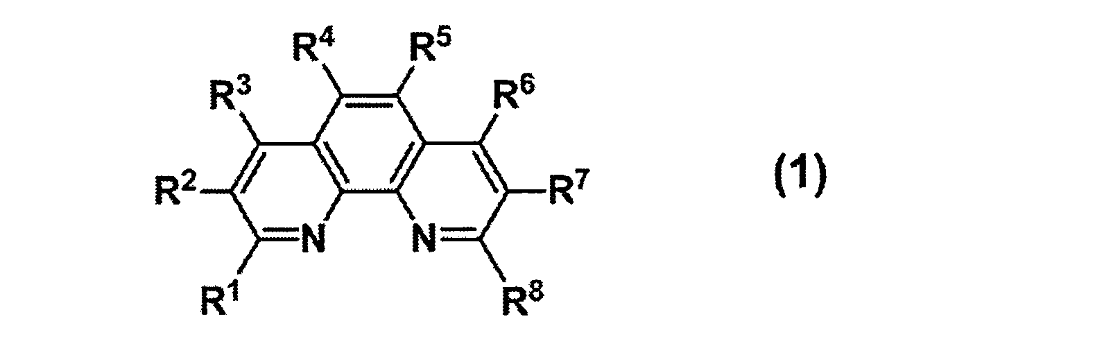

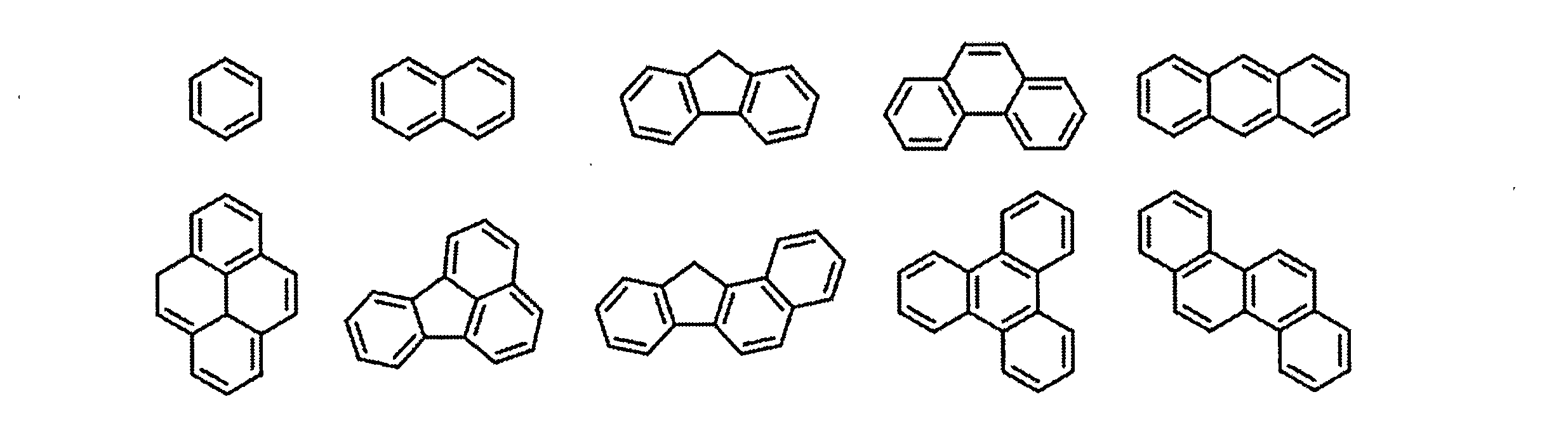

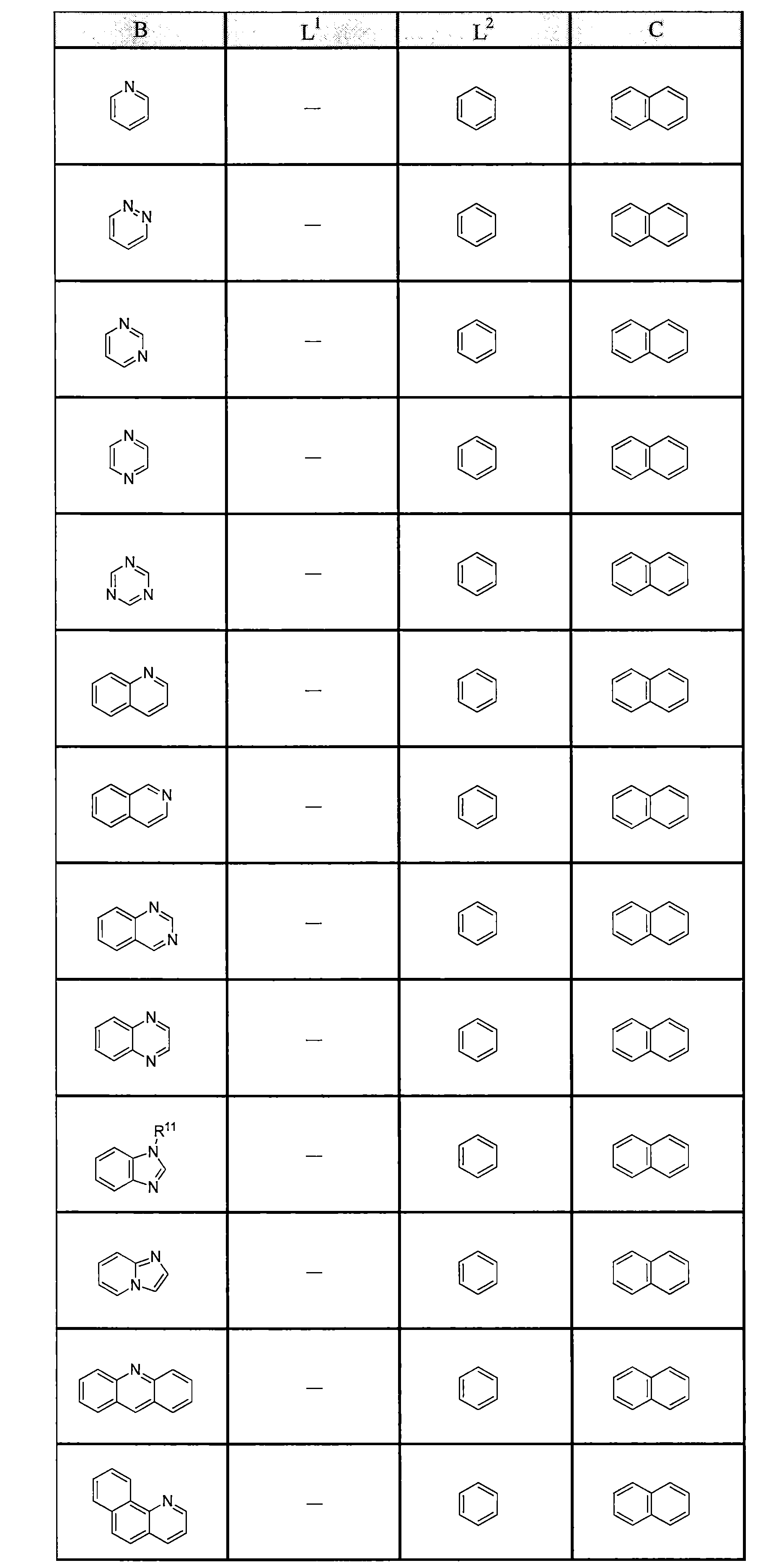

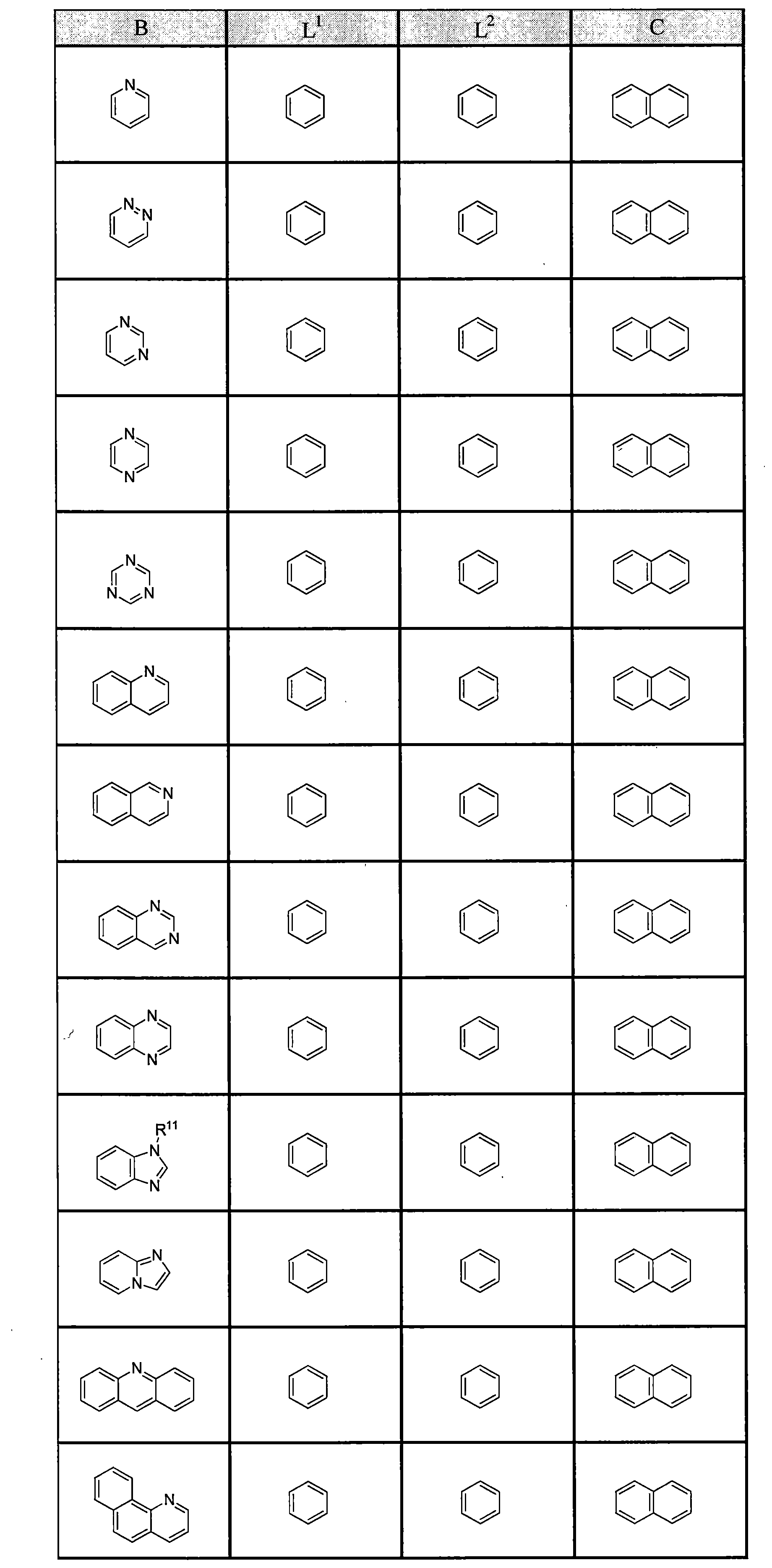


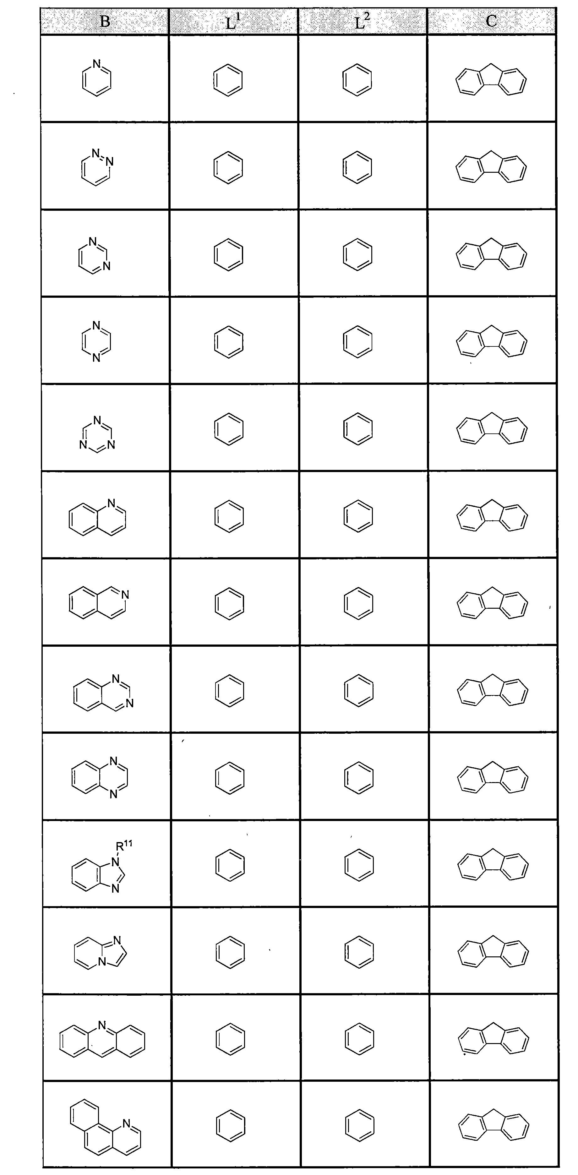


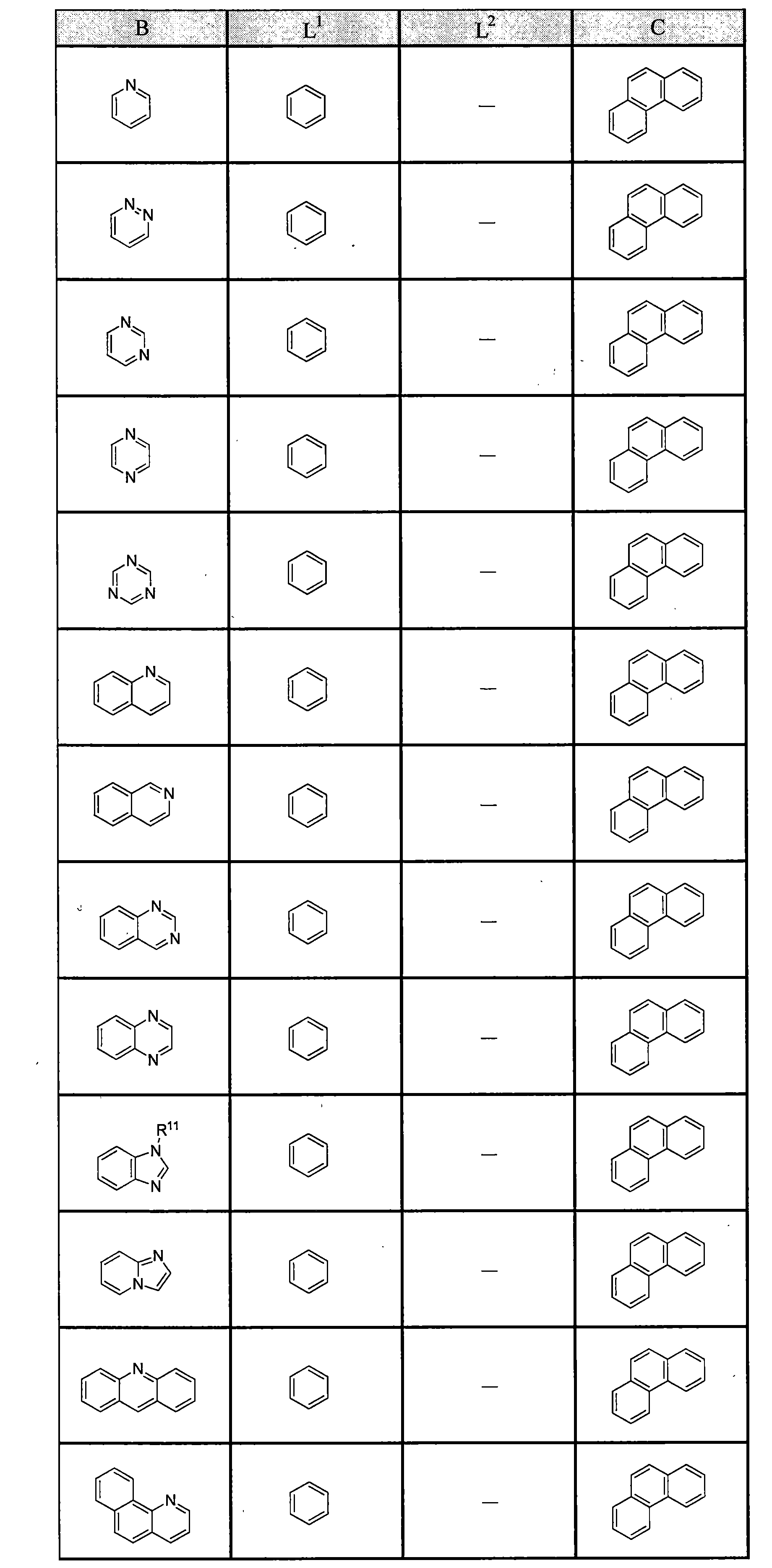
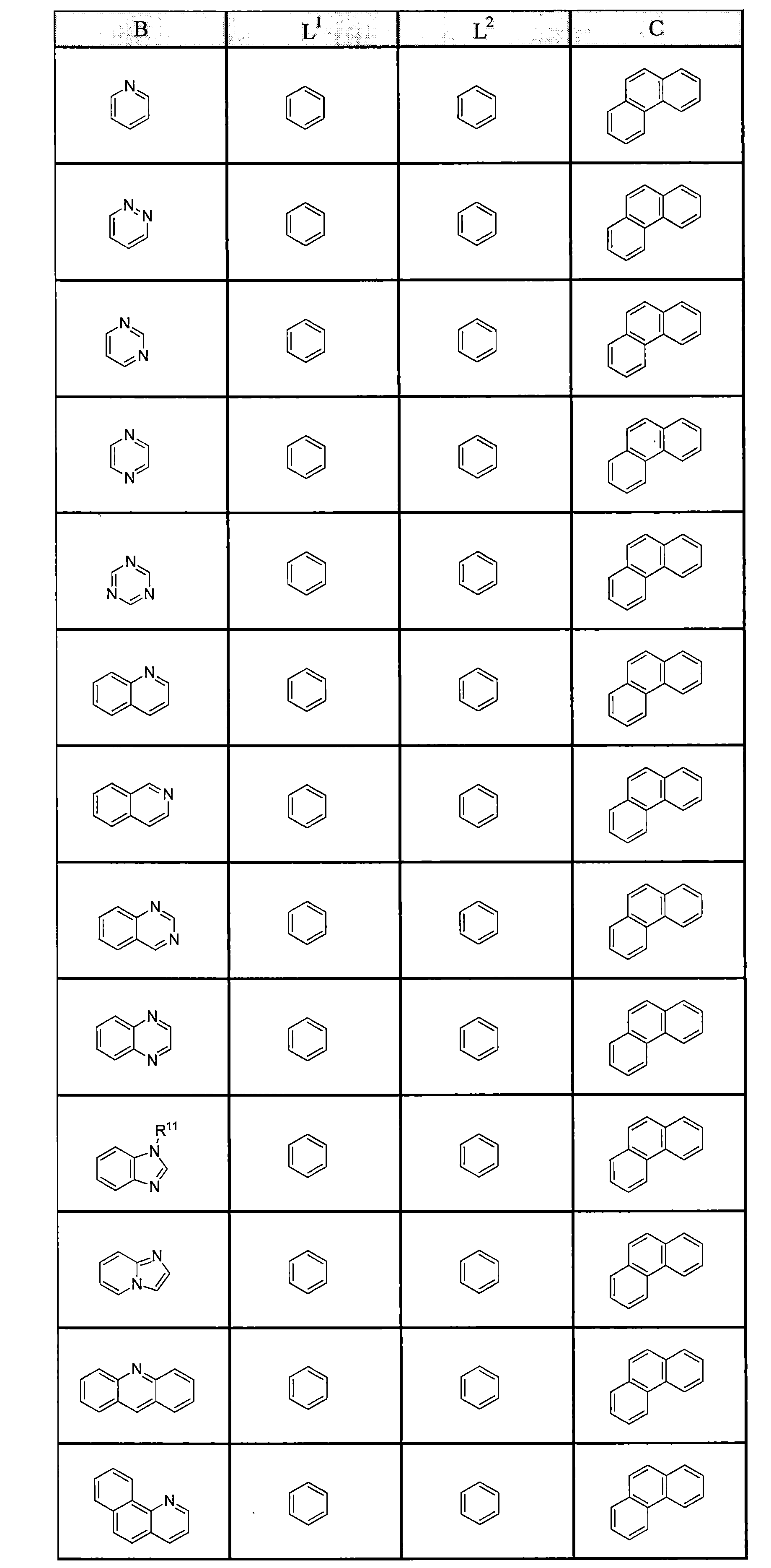


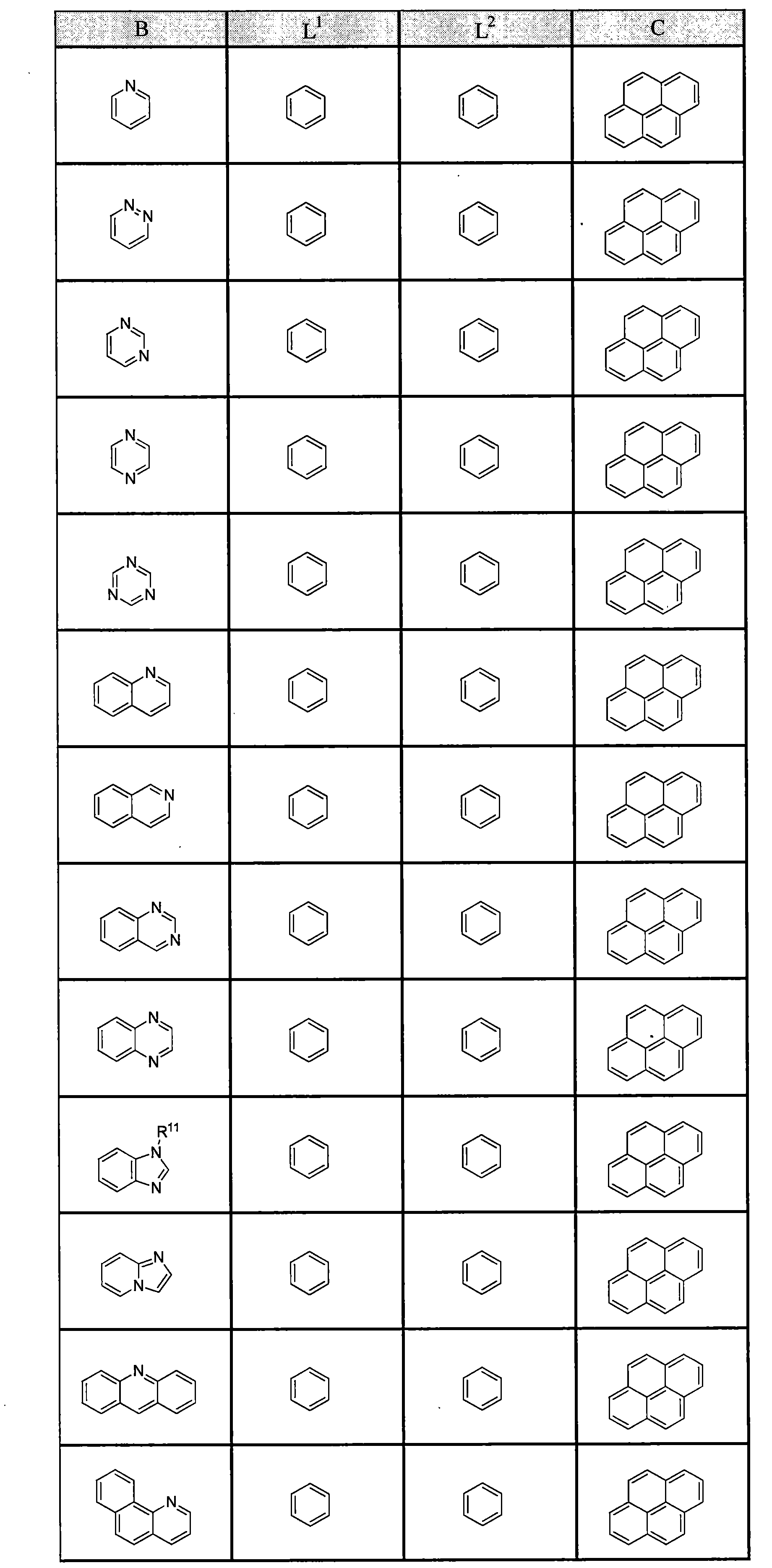

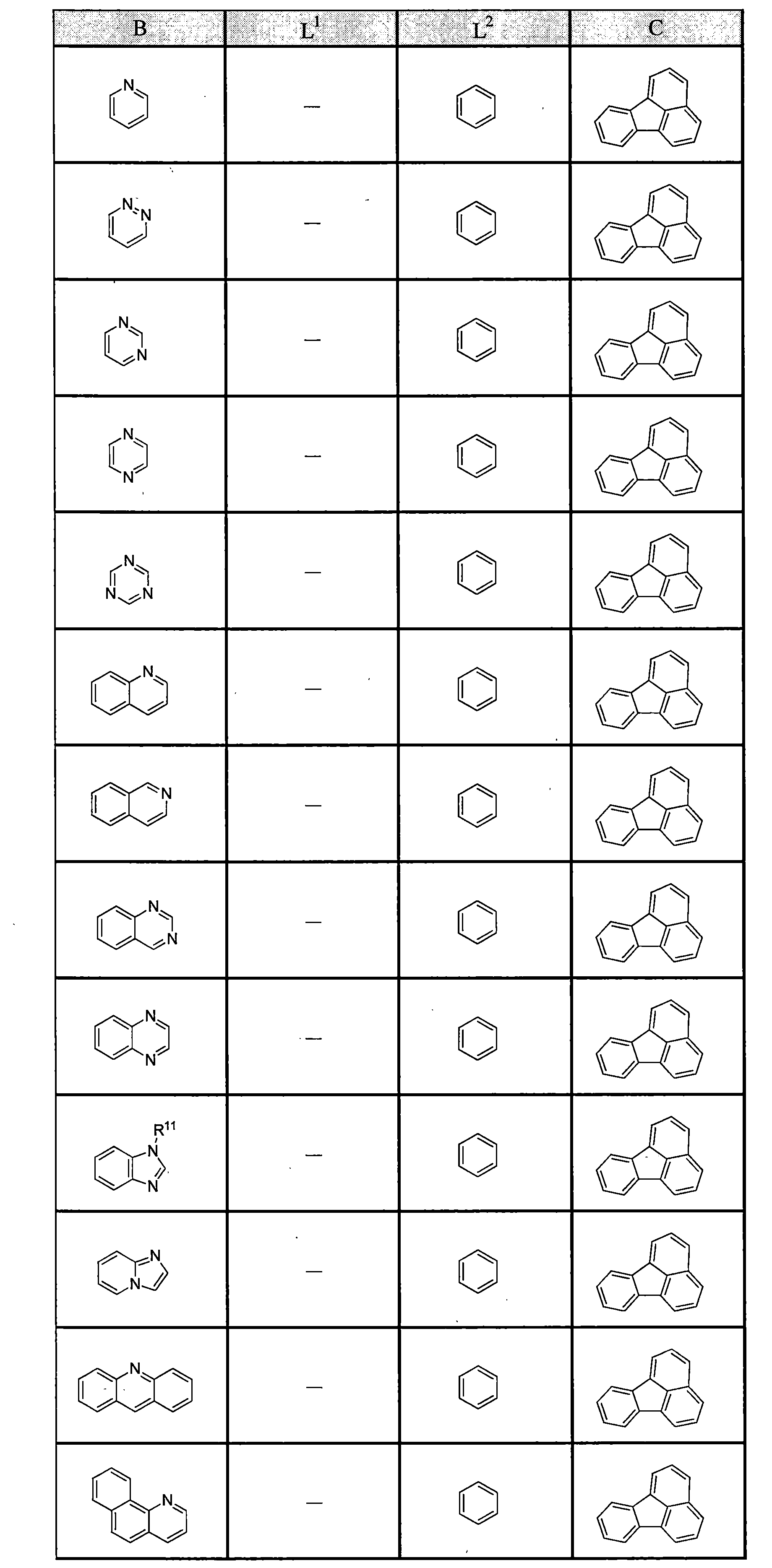
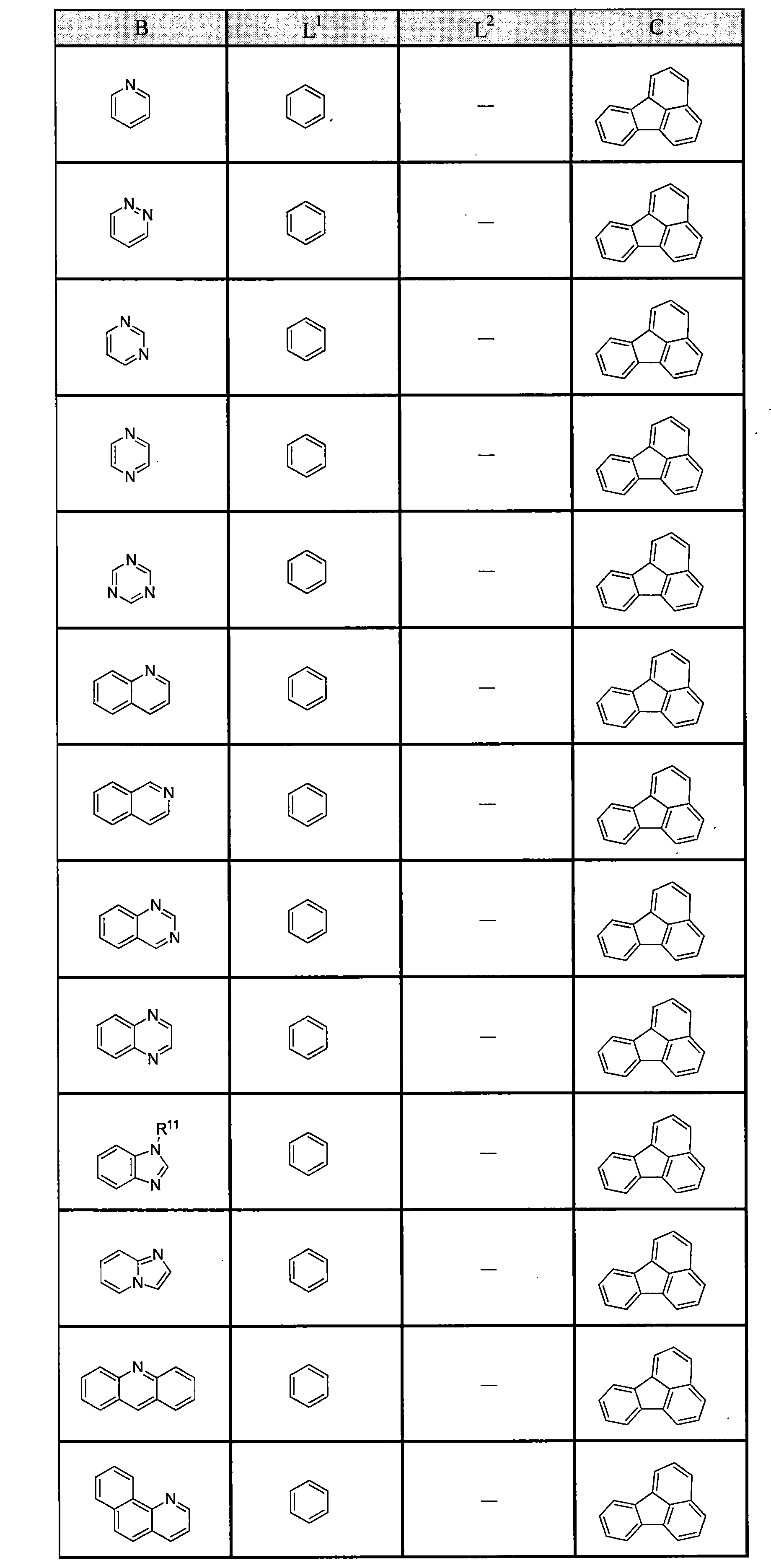
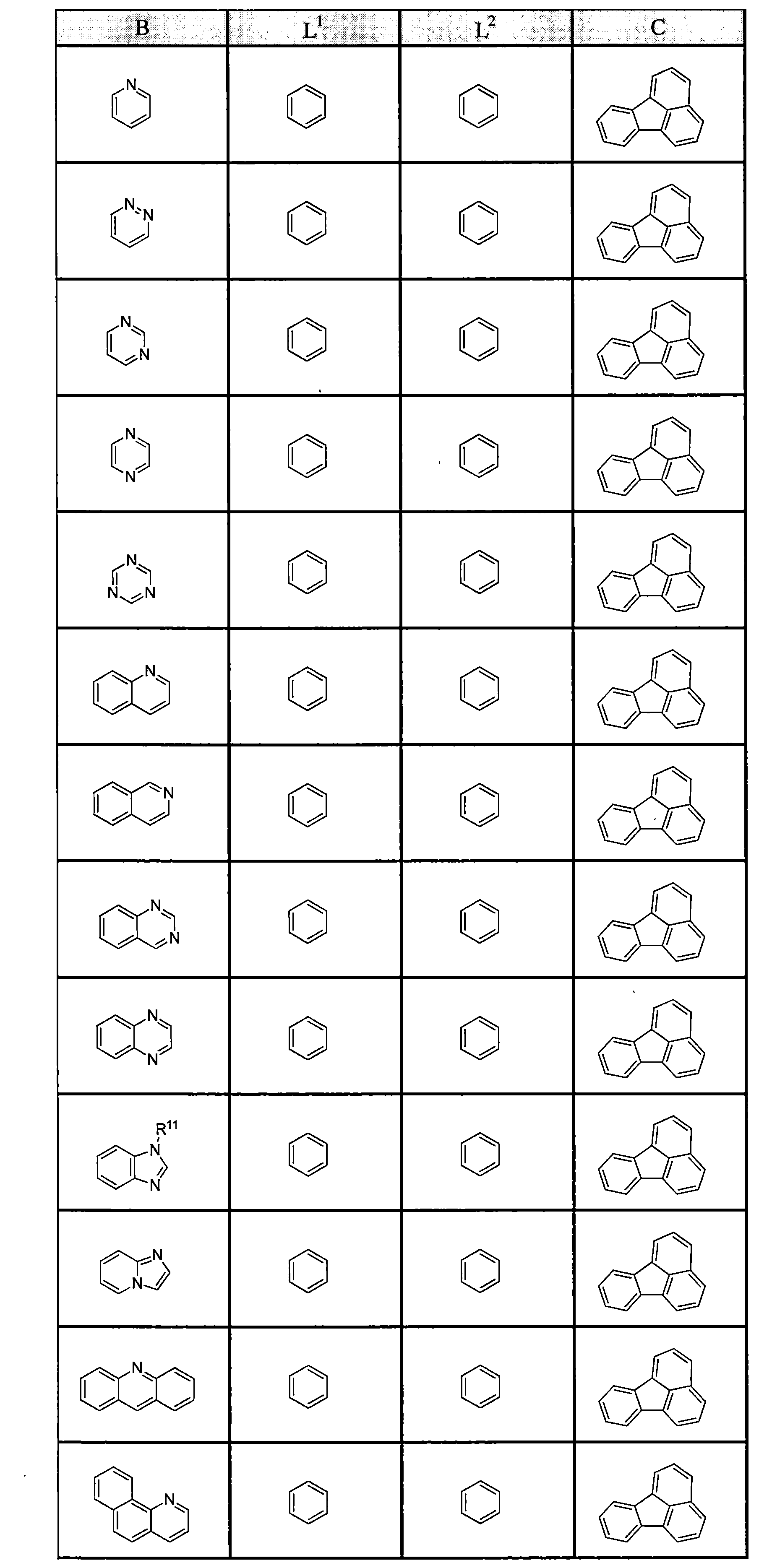

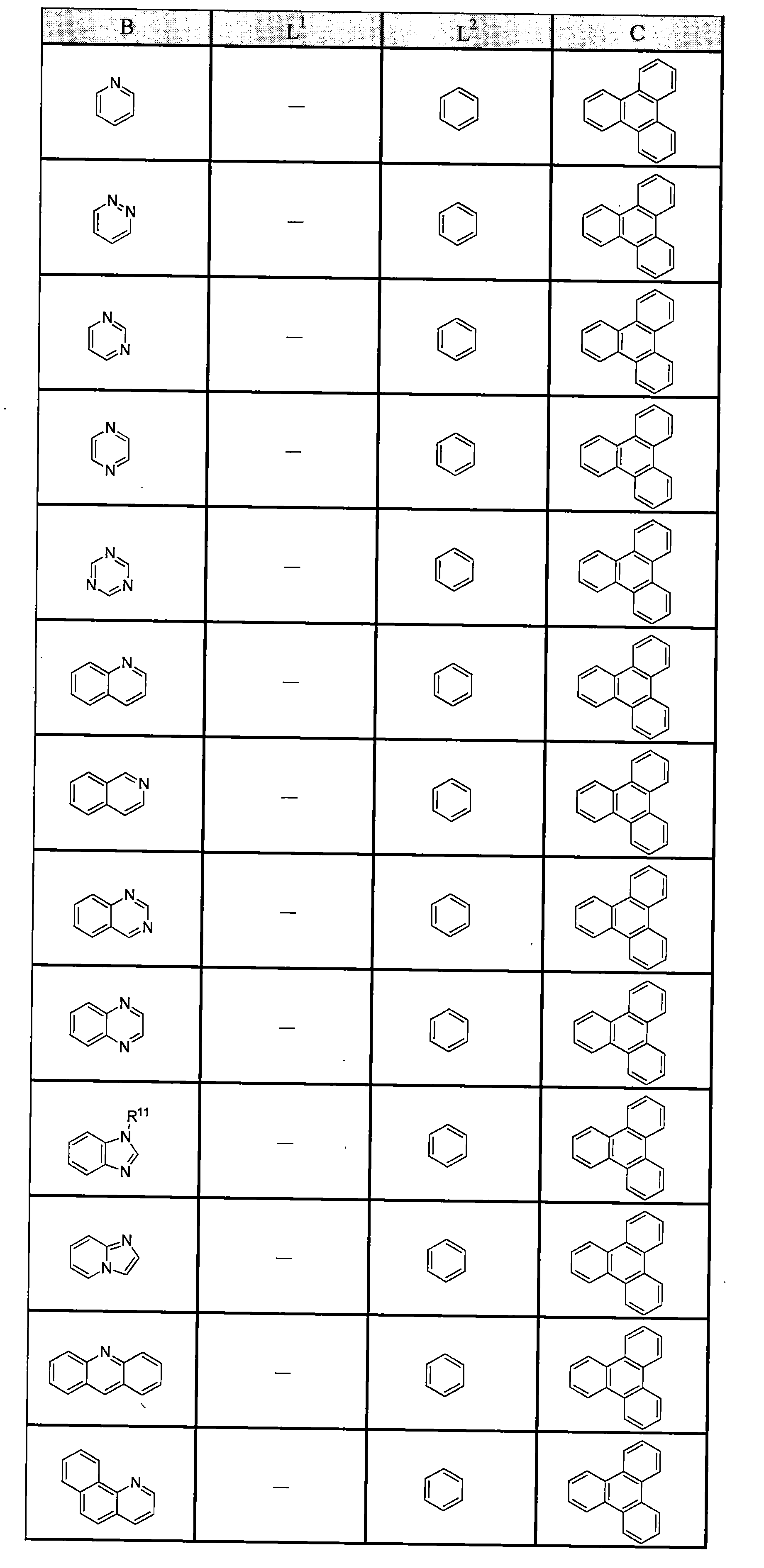

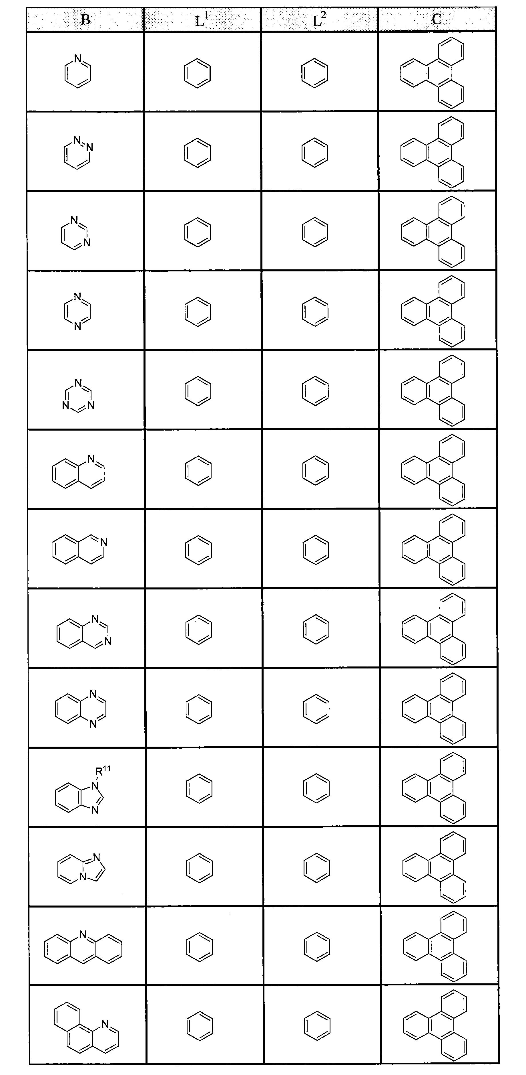
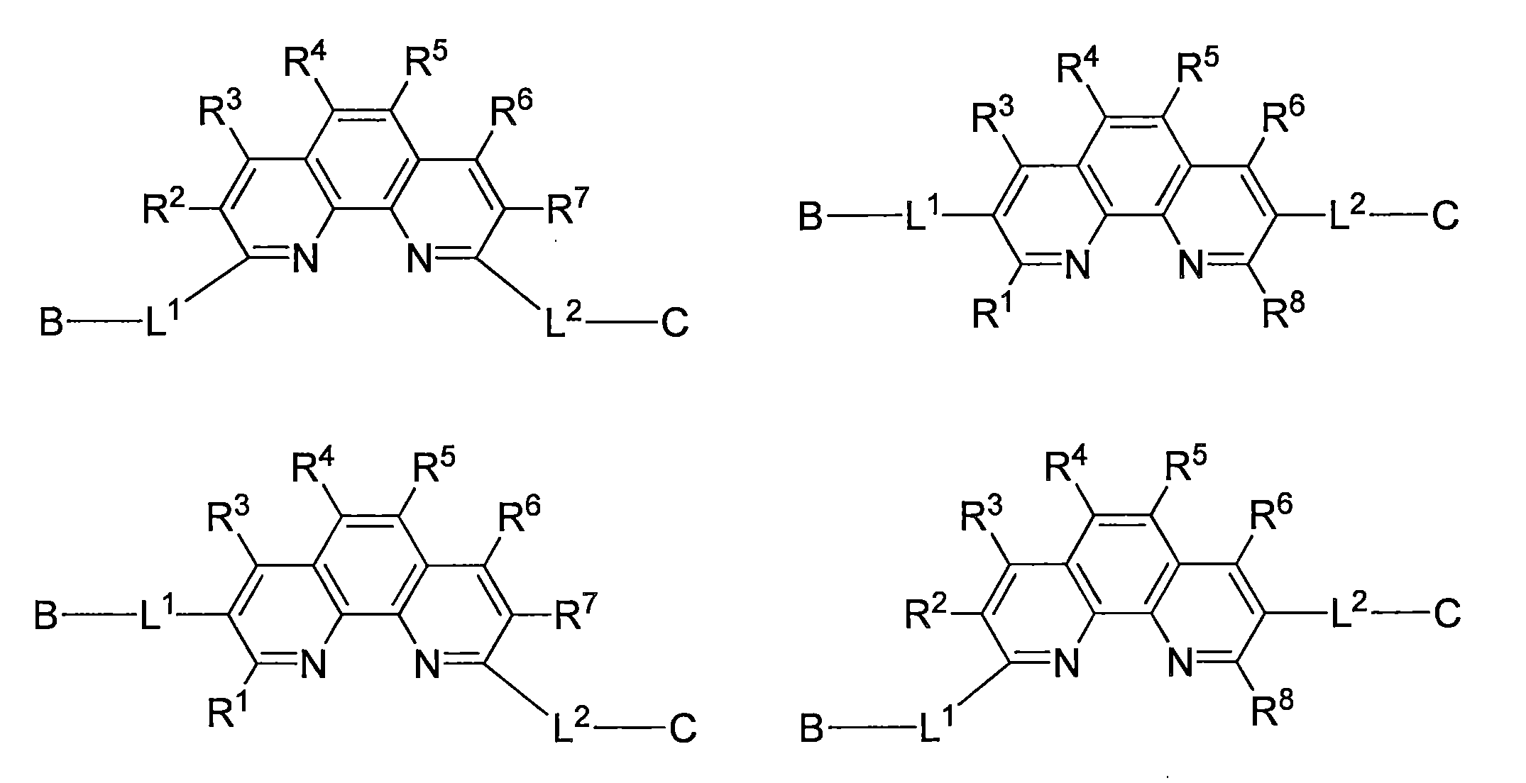


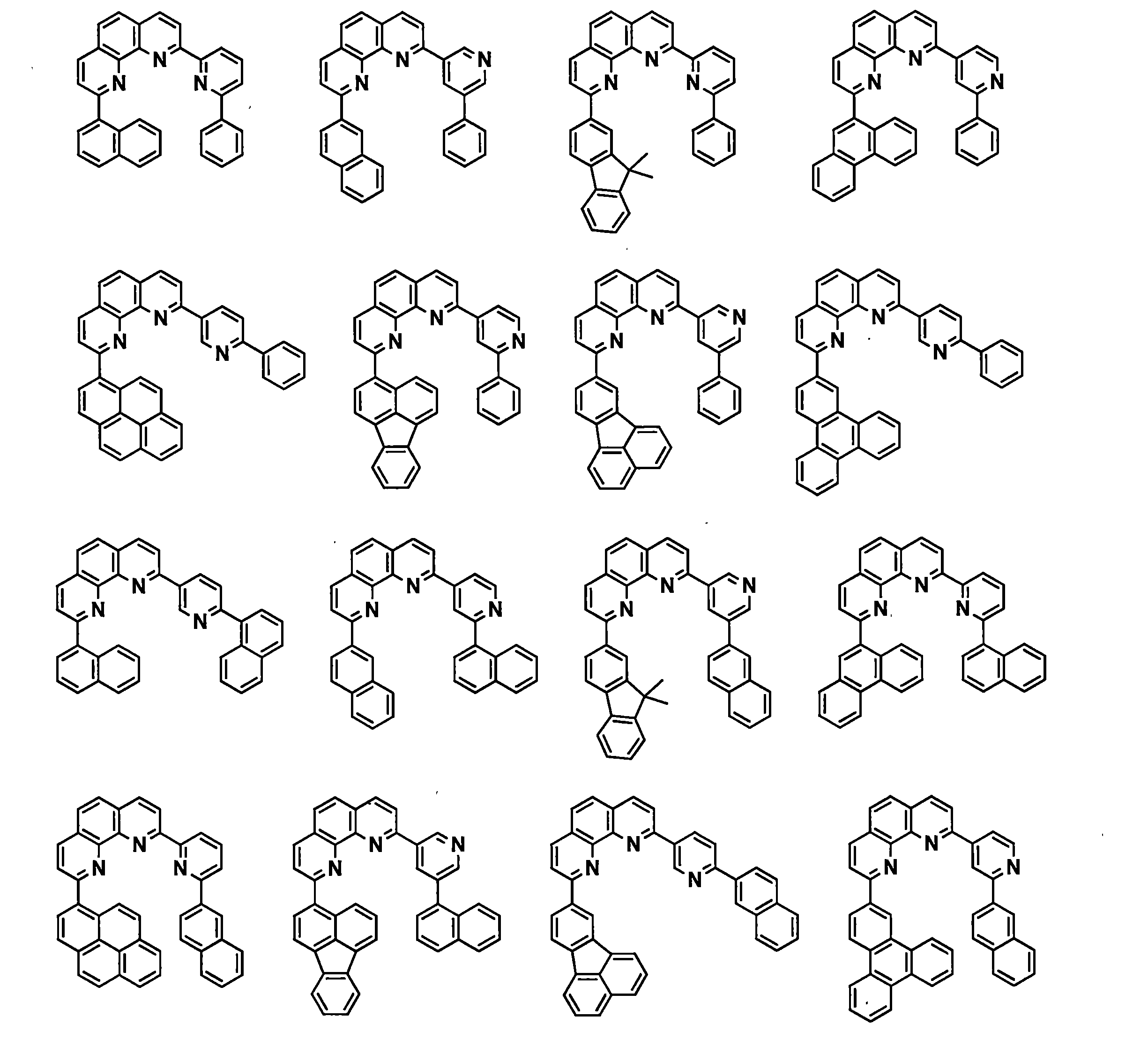
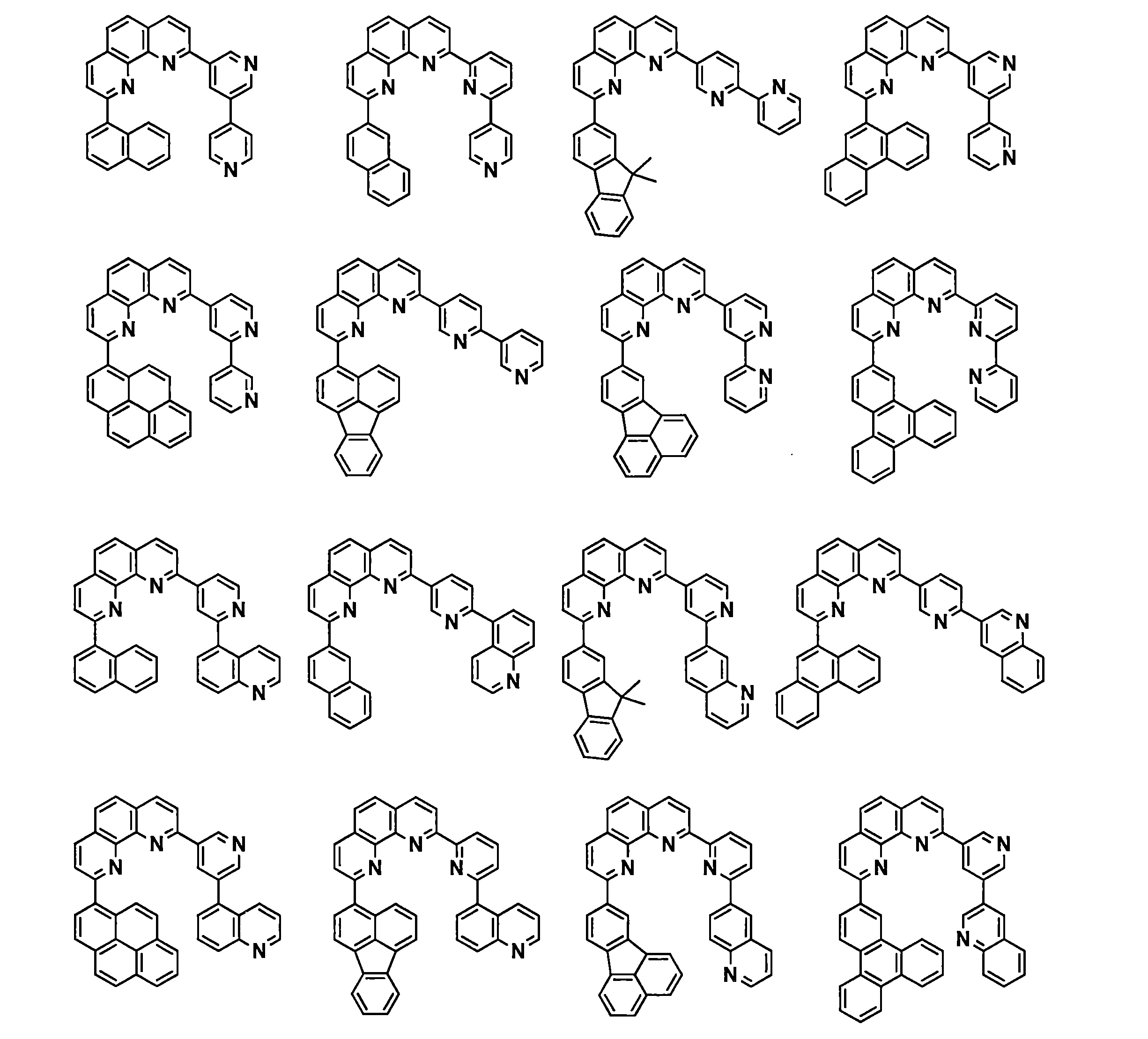

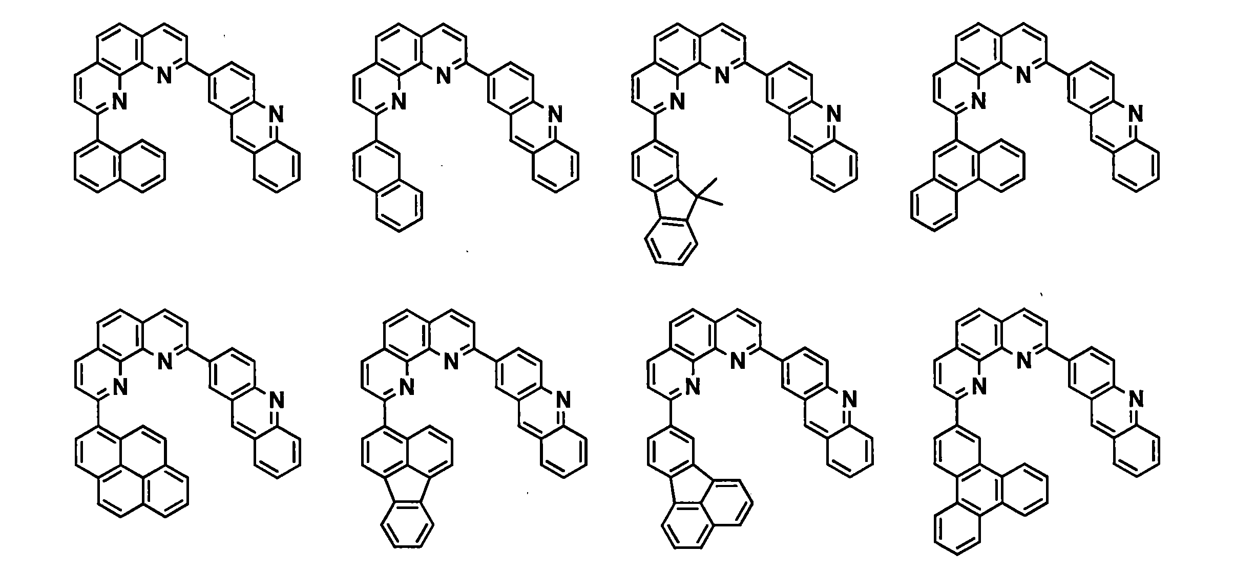
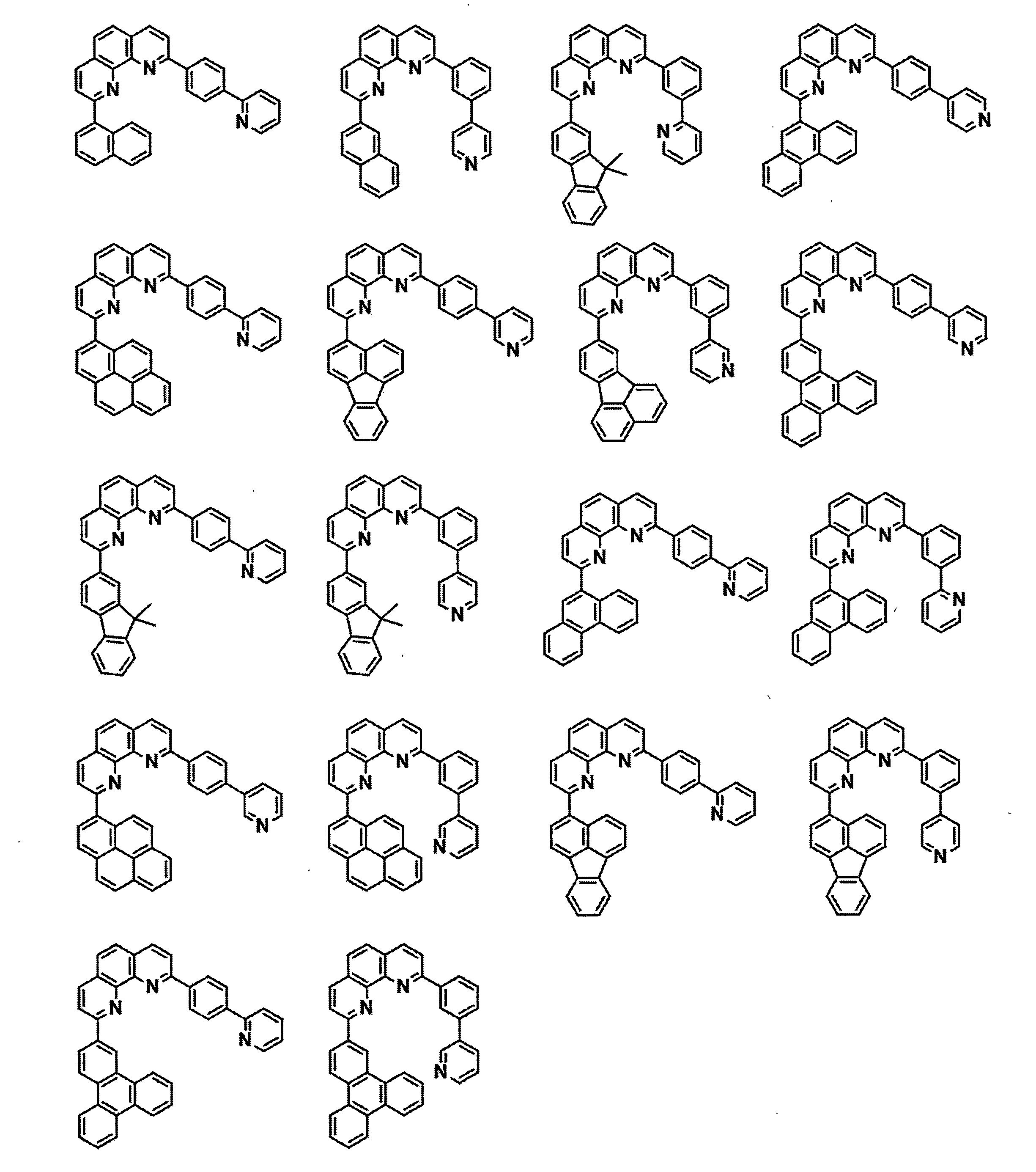


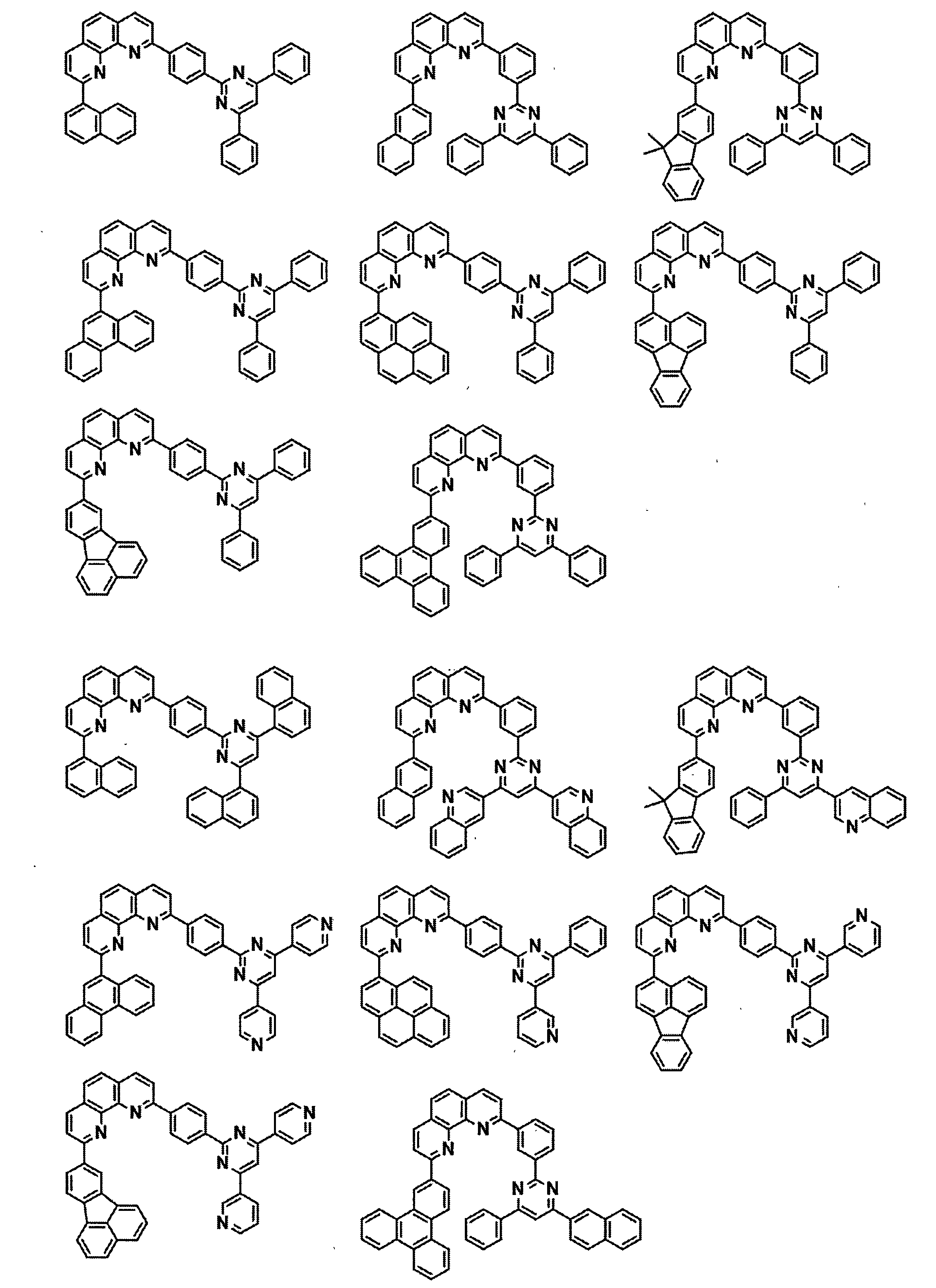
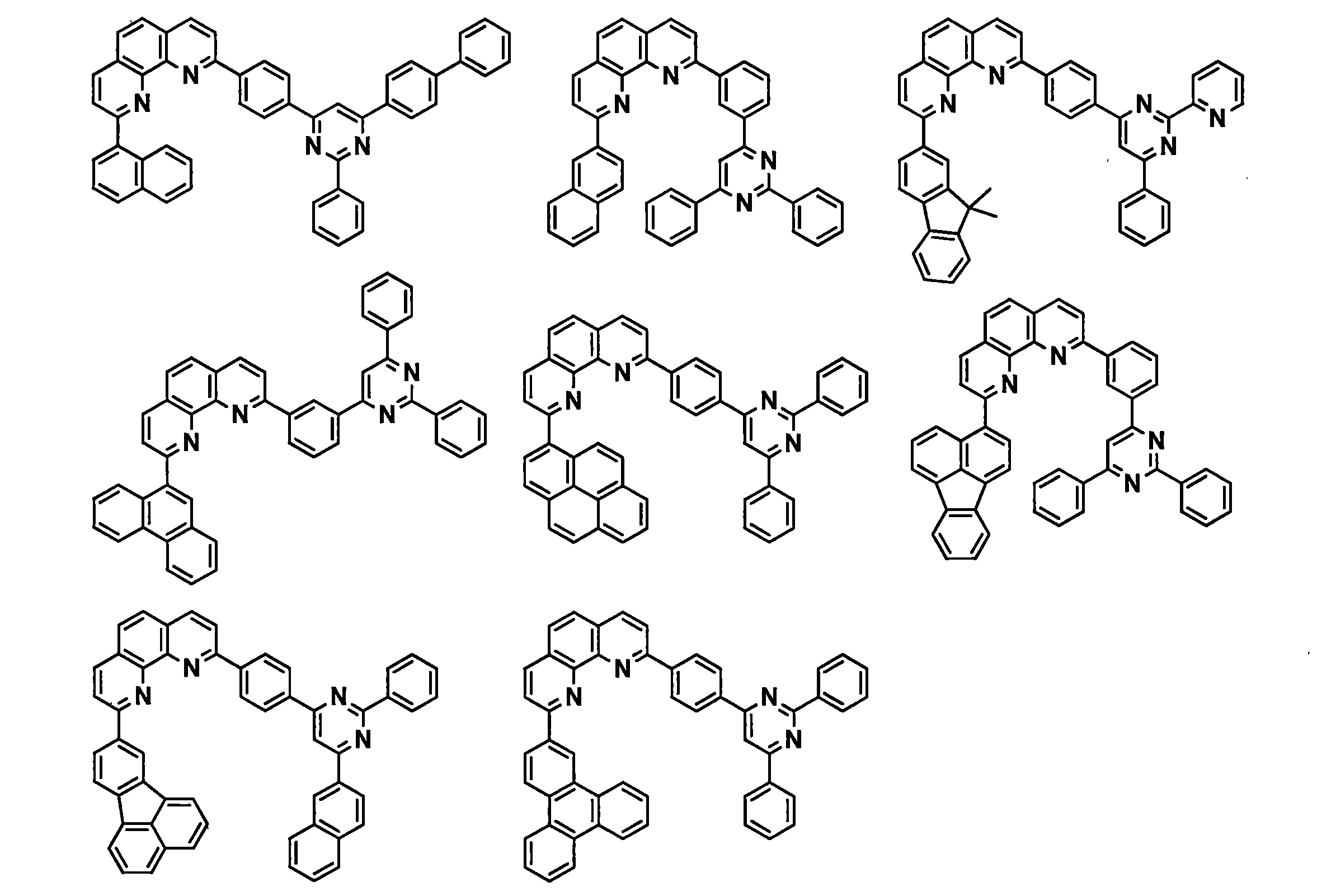
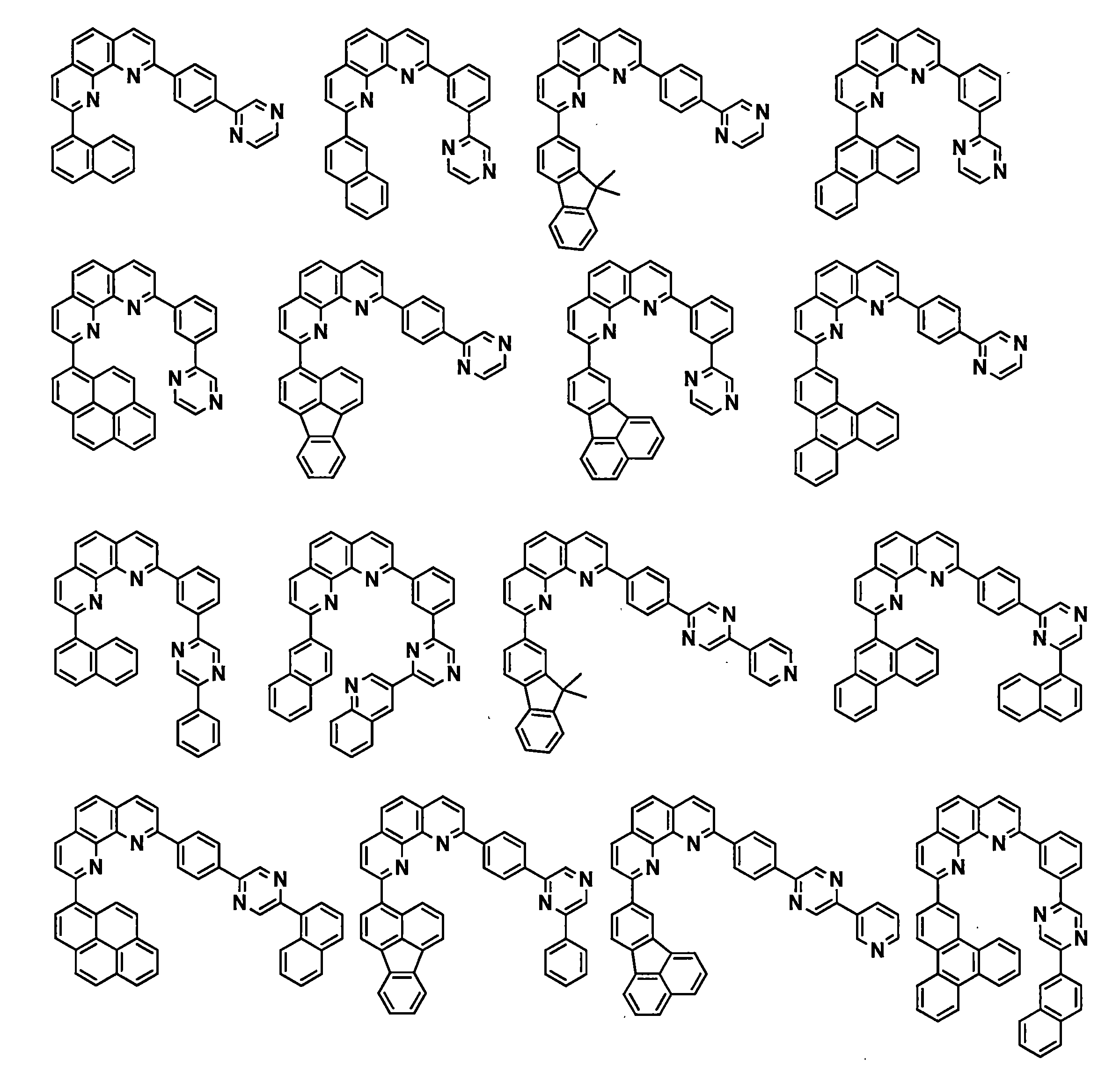
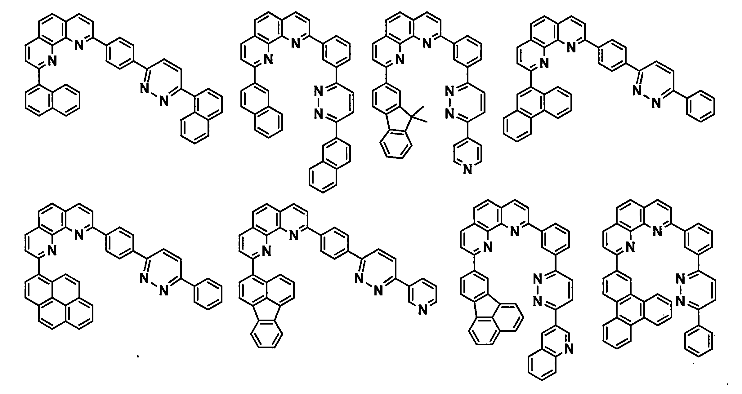


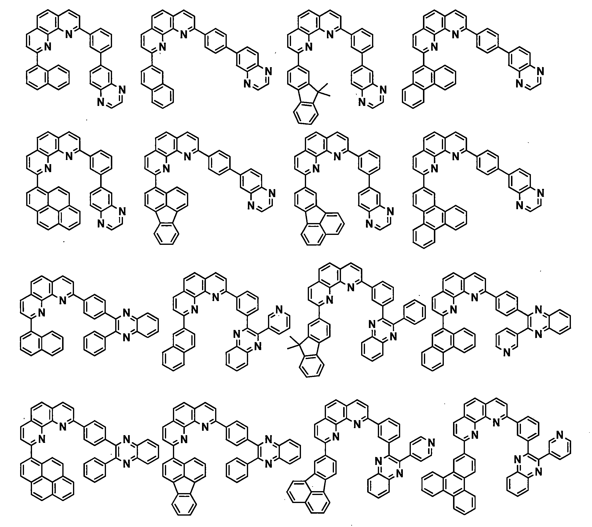


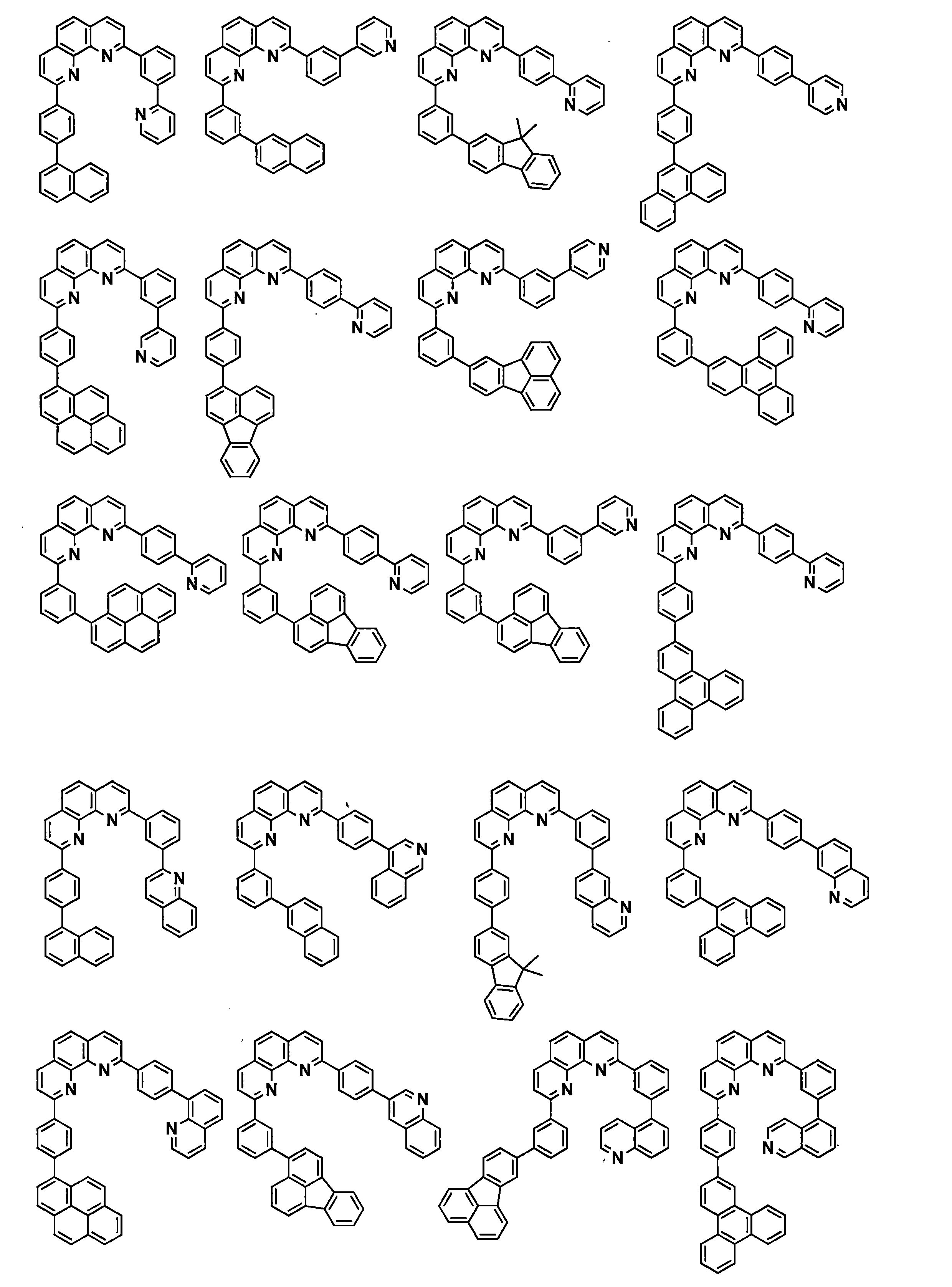


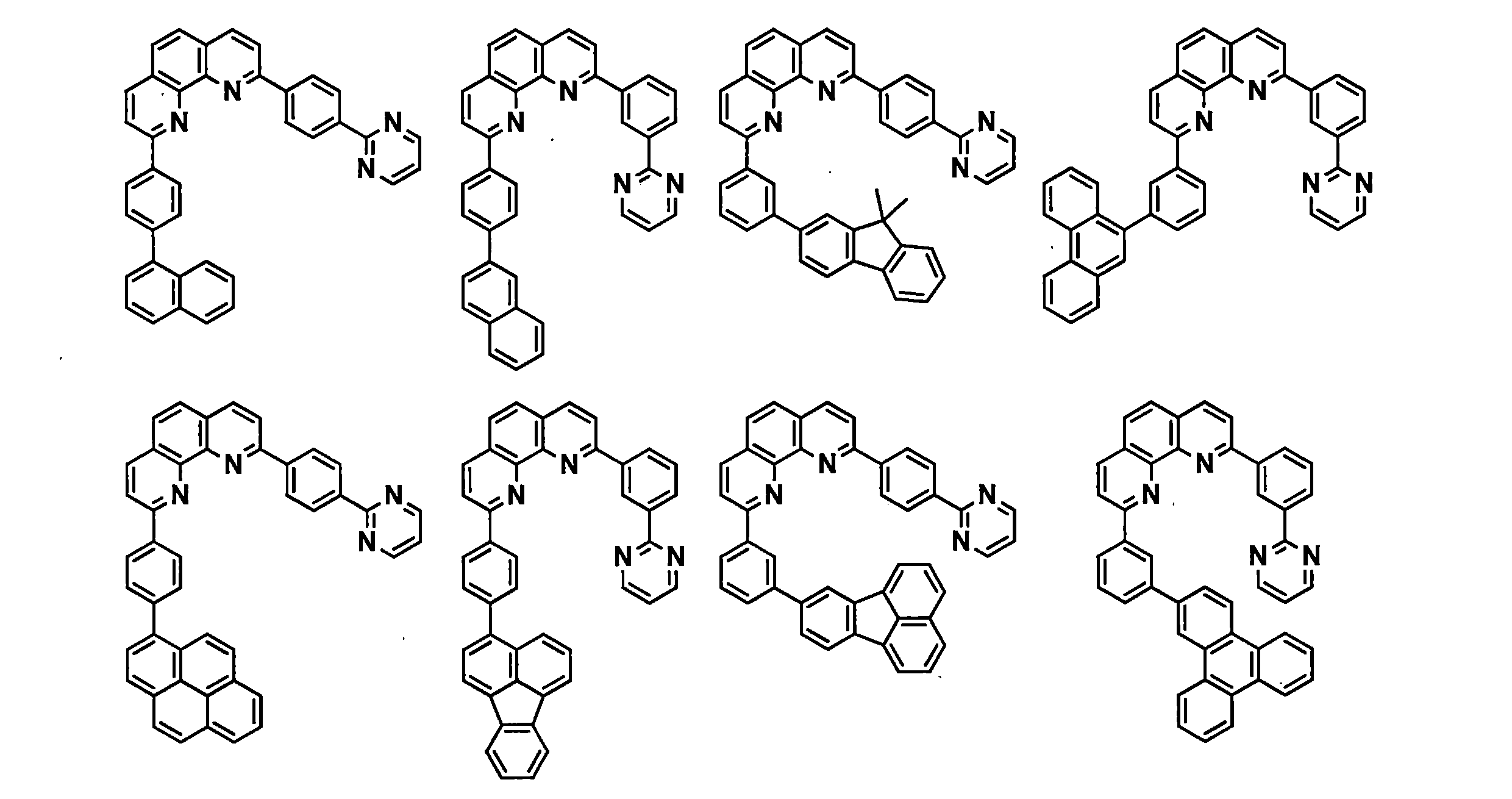

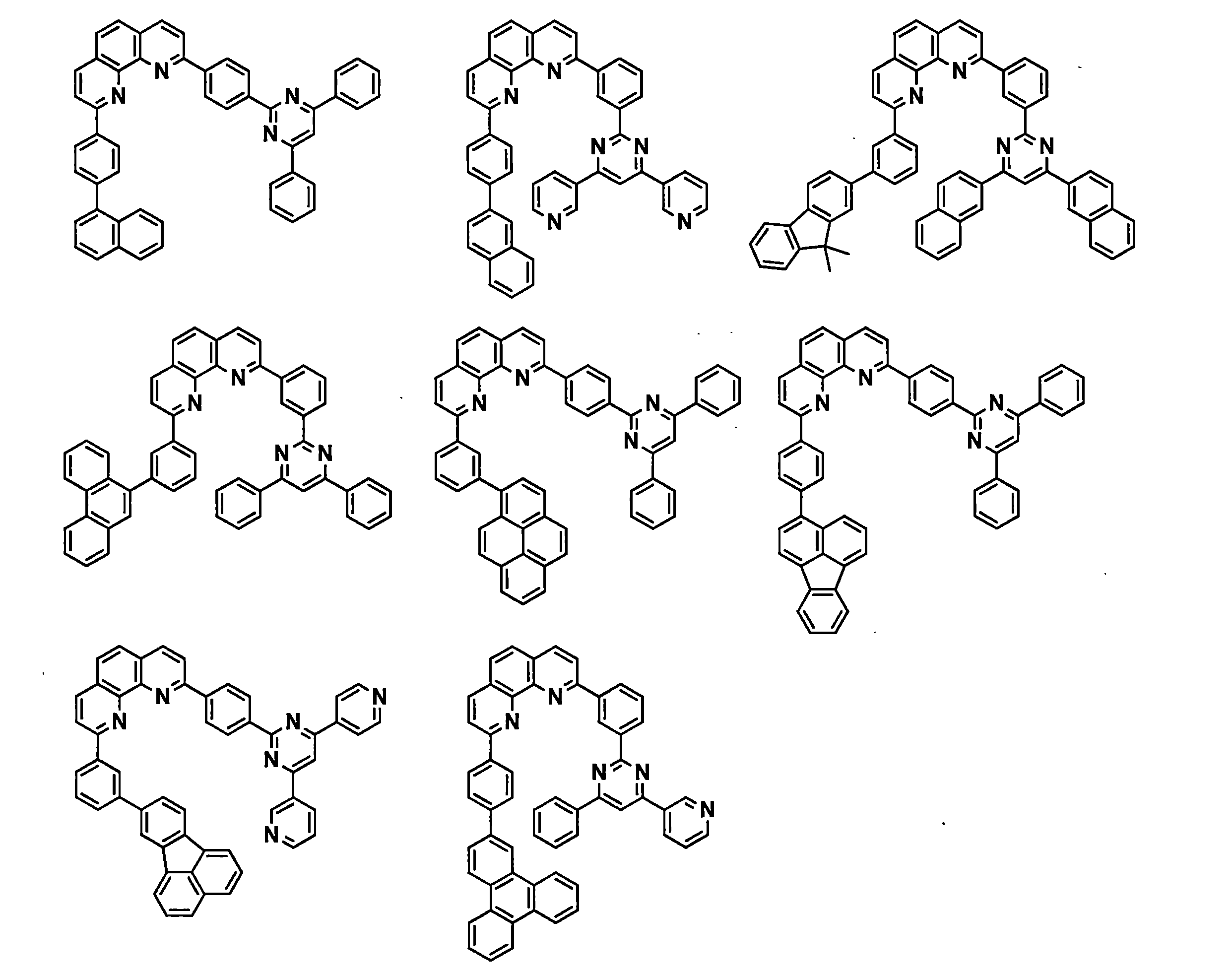
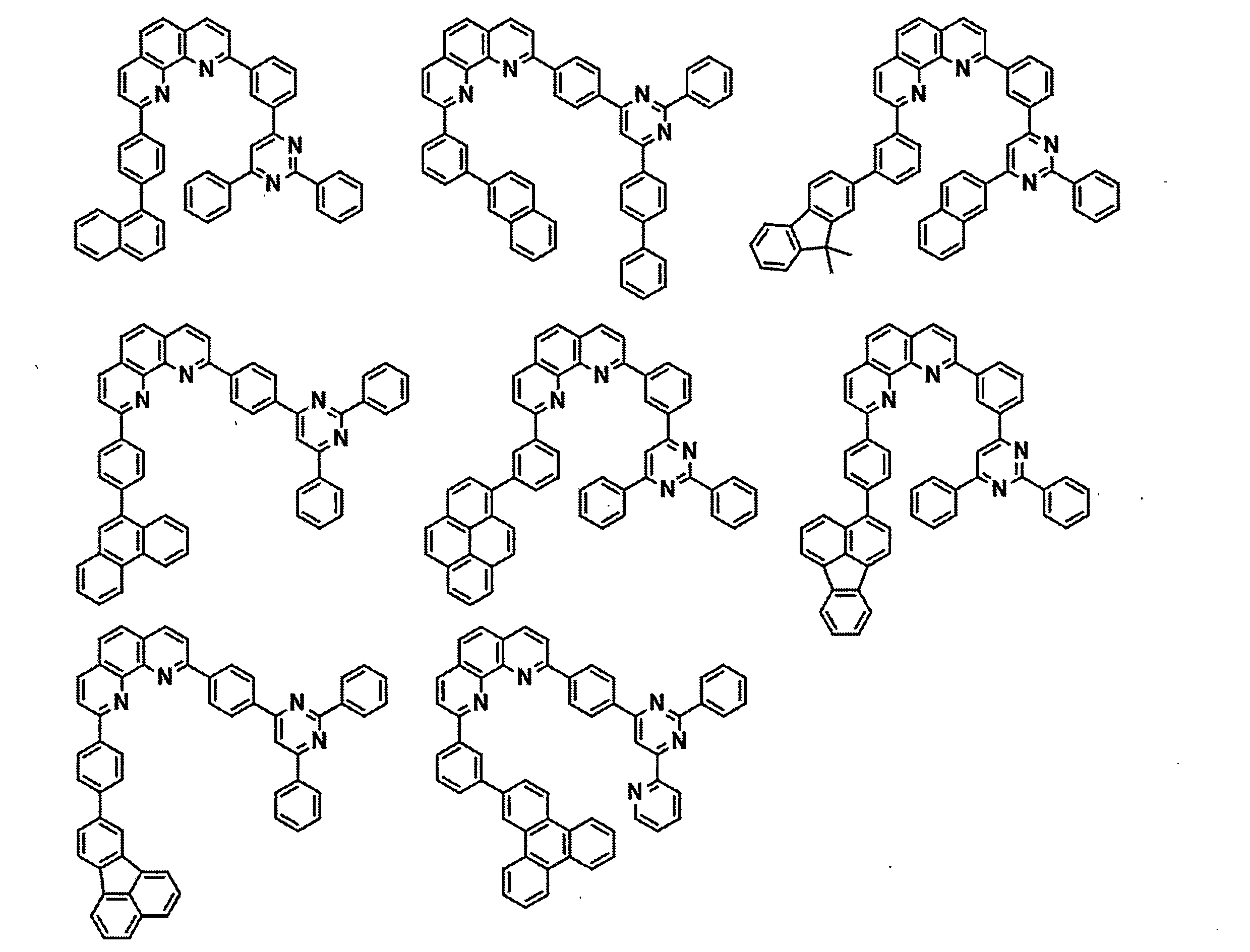

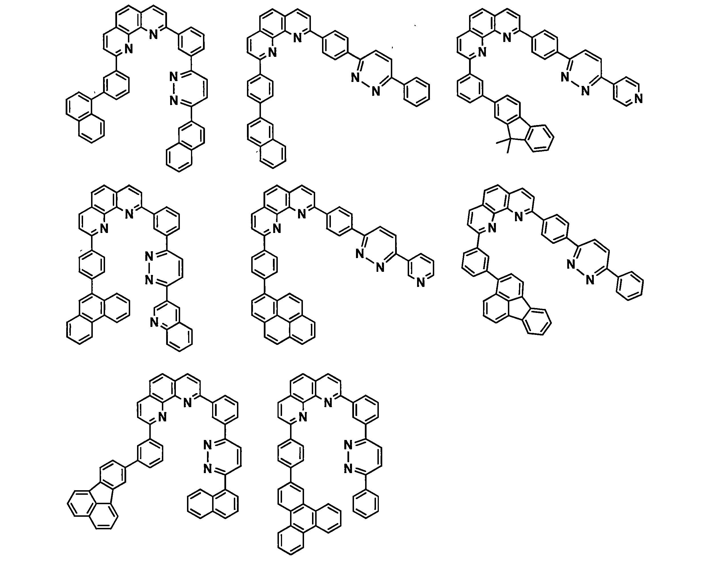
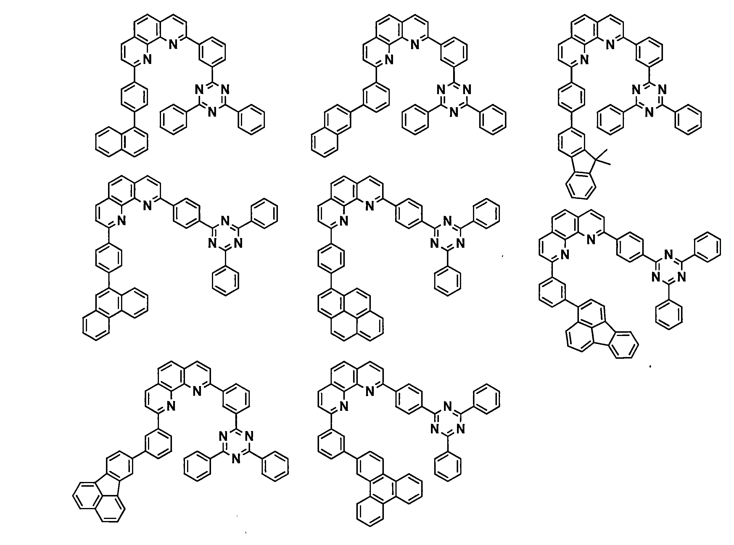
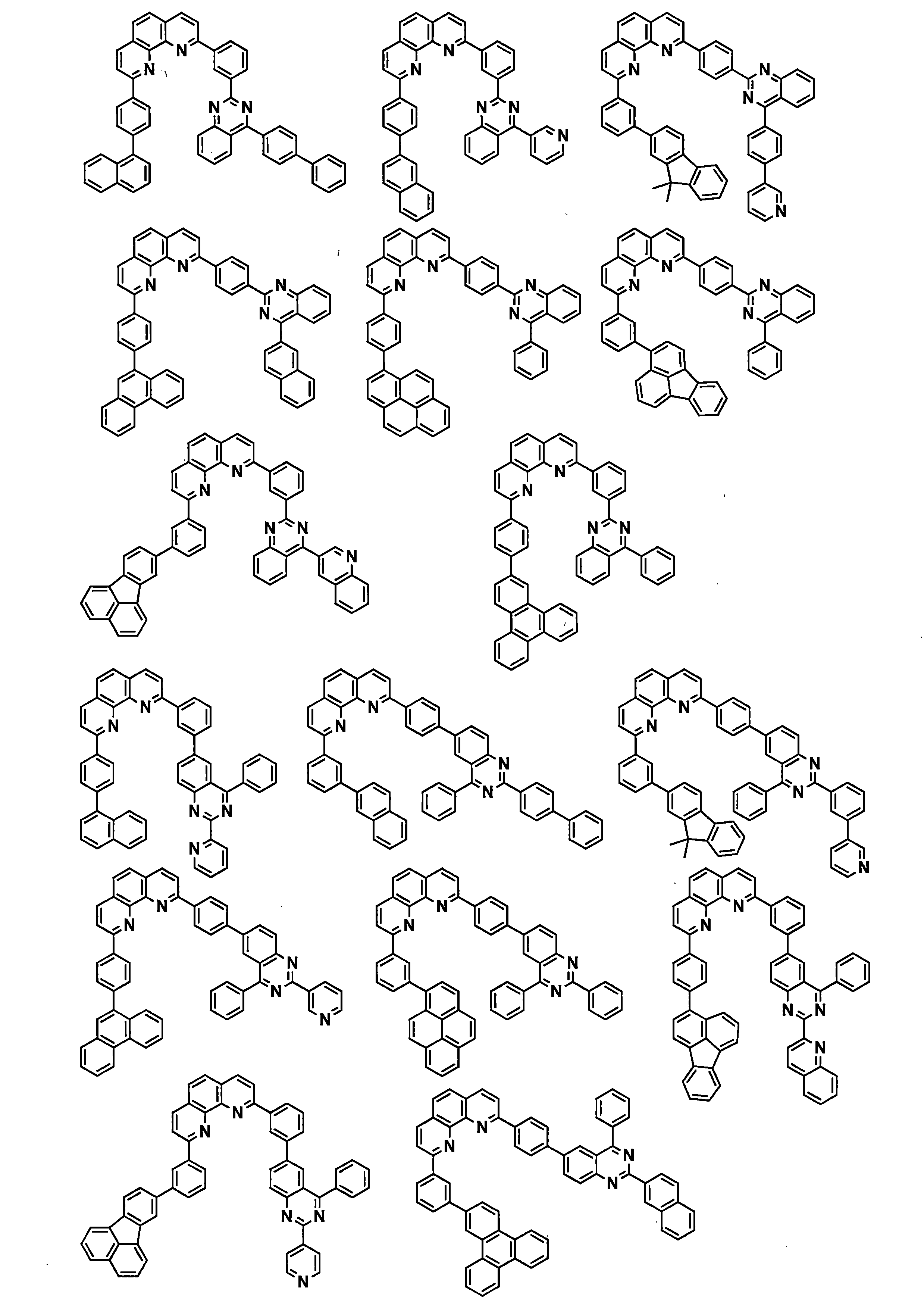


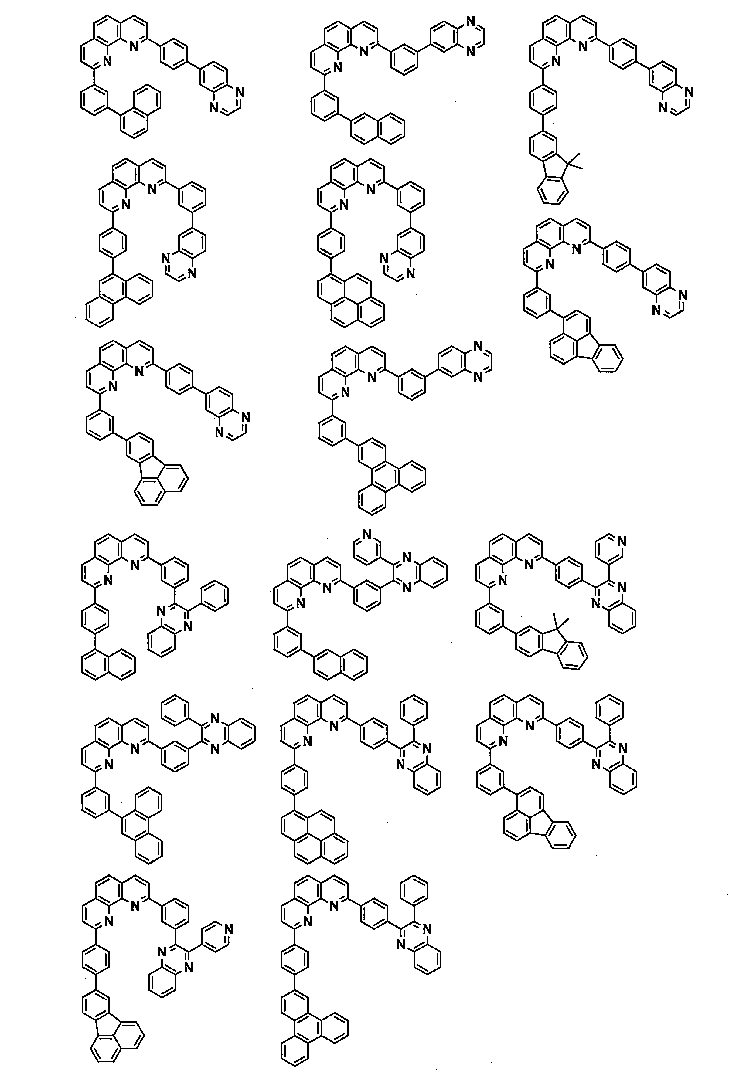
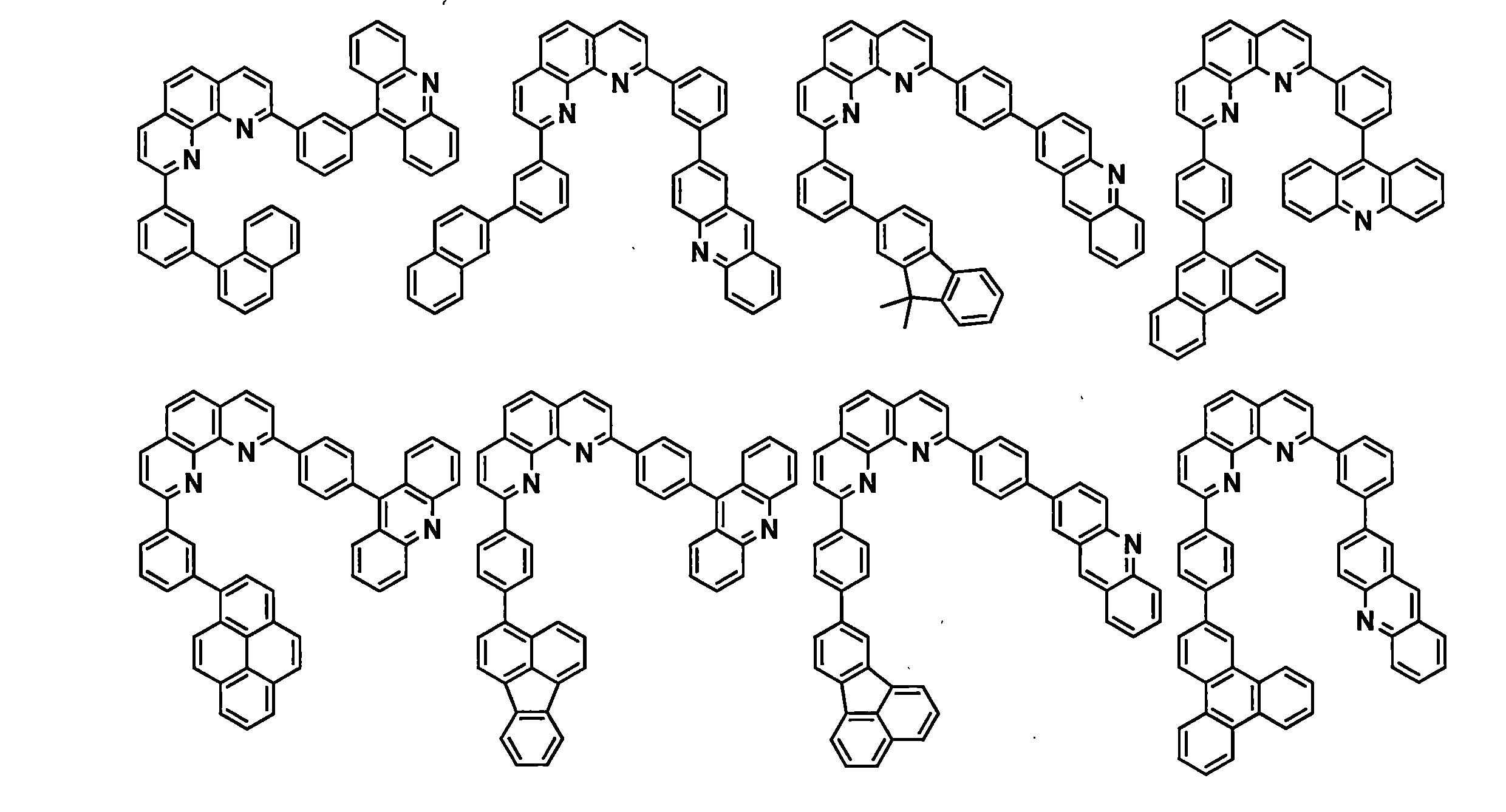
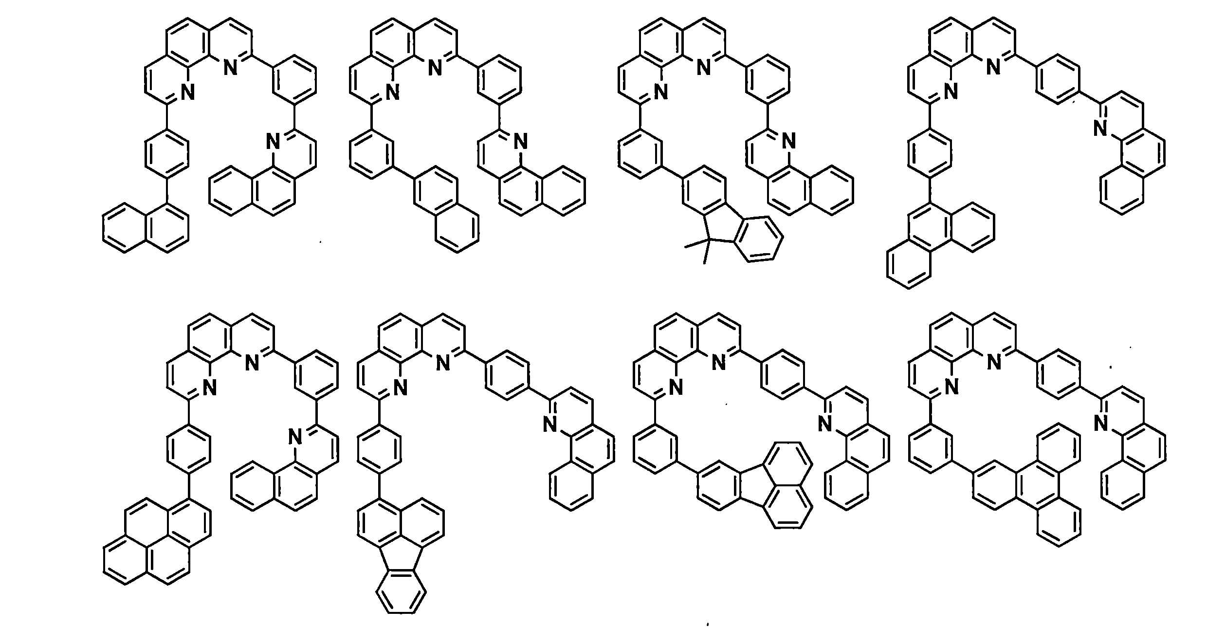


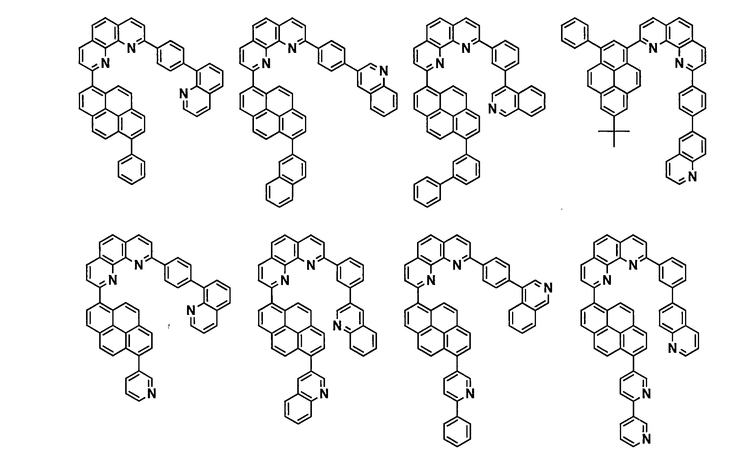
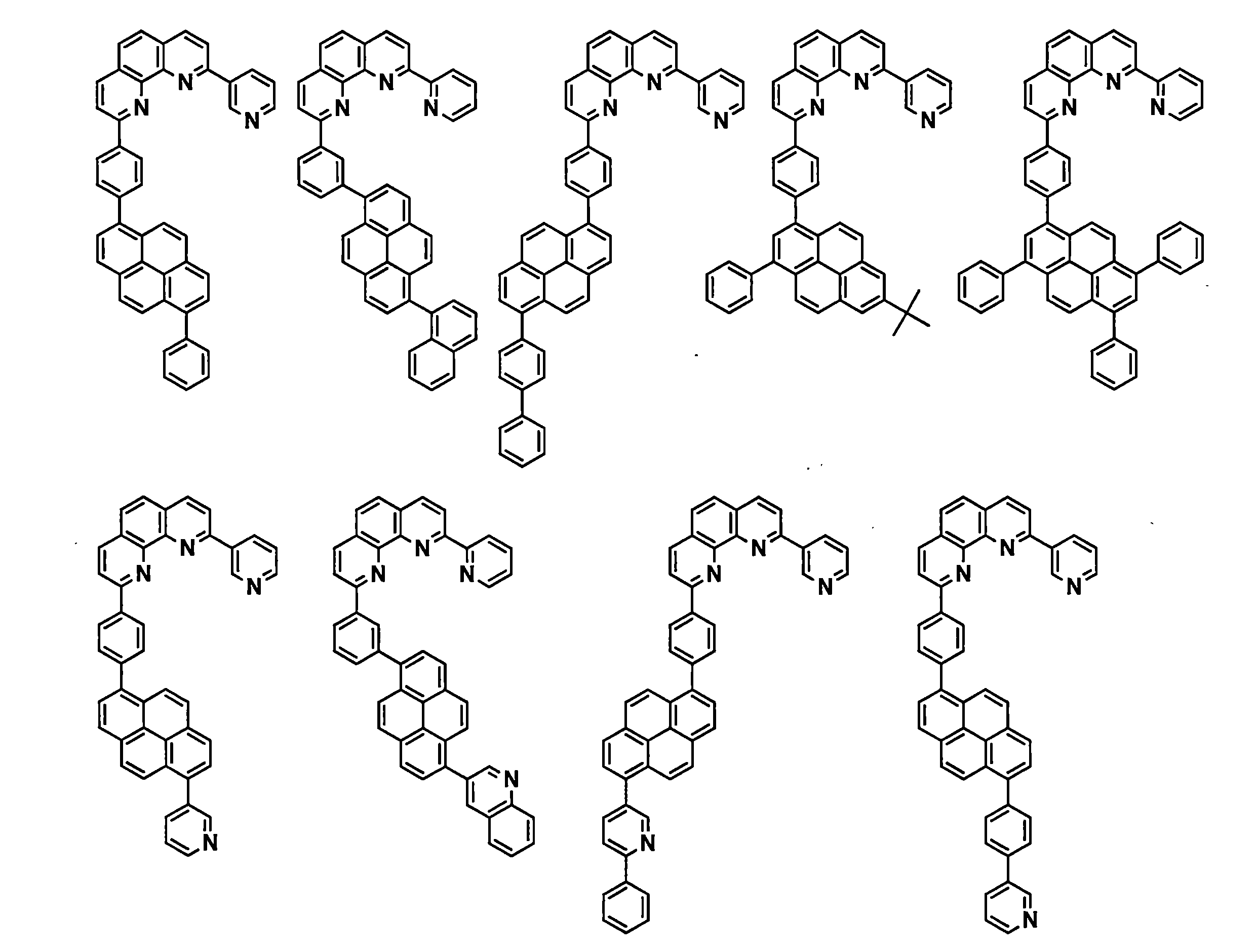

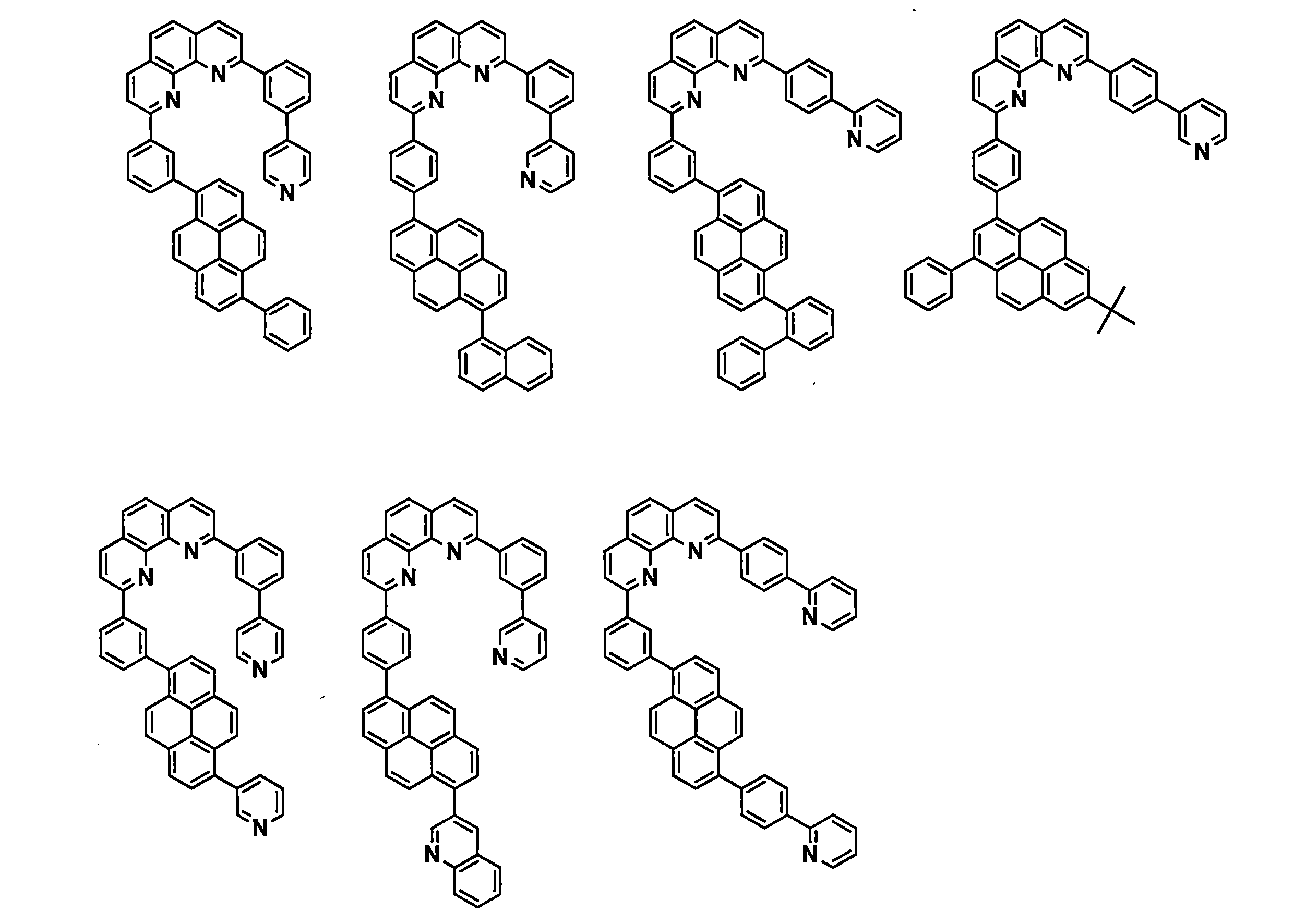

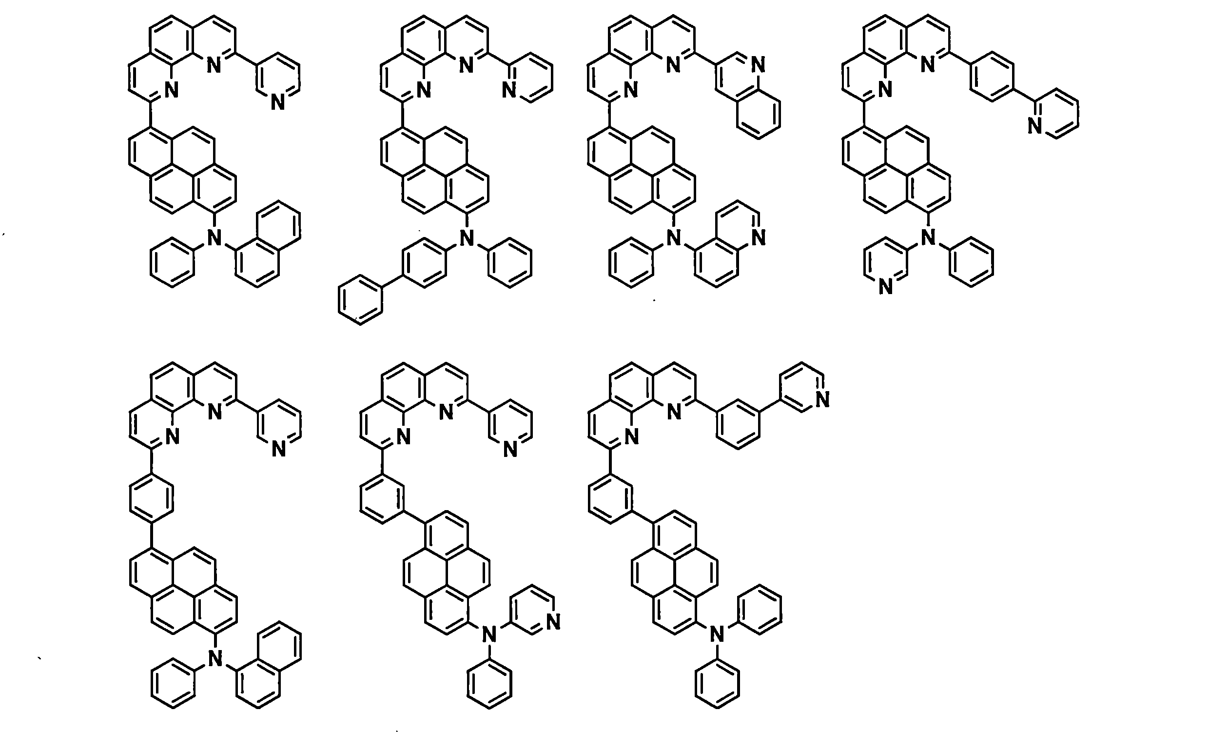

光電変換素子は、アノードとカソード、およびそれらアノードとカソードとの間に介在する有機層を有し、有機層において光エネルギーが電気的信号に変換される。前記有機層は少なくとも光電変換層を有していることが好ましく、さらに前記光電変換層はp型材料とn型材料を含むことがより好ましい。p型材料は、電子供与性(ドナー性)の材料であり、HOMOのエネルギー準位が浅く、正孔を輸送しやすい。n型材料は、電子吸引性(アクセプター性)の材料であり、LUMOのエネルギー準位が深く、電子を輸送しやすい。p型材料とn型材料は積層されていてもよいし、混合されていてもよい。
次に、本発明の発光素子の実施の形態について詳細に説明する。本発明の発光素子は、陽極と陰極、およびそれら陽極と陰極との間に介在する有機層を有し、該有機層が電気エネルギーにより発光する。
本発明の発光素子において、陽極と陰極は素子の発光のために十分な電流を供給するための役割を有するものであり、光を取り出すために少なくとも一方は透明または半透明であることが好ましい。通常、基板上に形成される陽極を透明電極とする。
正孔輸送層は、正孔輸送材料の一種または二種以上を積層または混合する方法、もしくは、正孔輸送材料と高分子結着剤の混合物を用いる方法により形成される。また、正孔輸送材料は、電界を与えられた電極間において正極からの正孔を効率良く輸送することが必要で、正孔注入効率が高く、注入された正孔を効率良く輸送することが好ましい。そのためには適切なイオン化ポテンシャルを持ち、しかも正孔移動度が大きく、さらに安定性に優れ、トラップとなる不純物が製造時および使用時に発生しにくい物質であることが要求される。
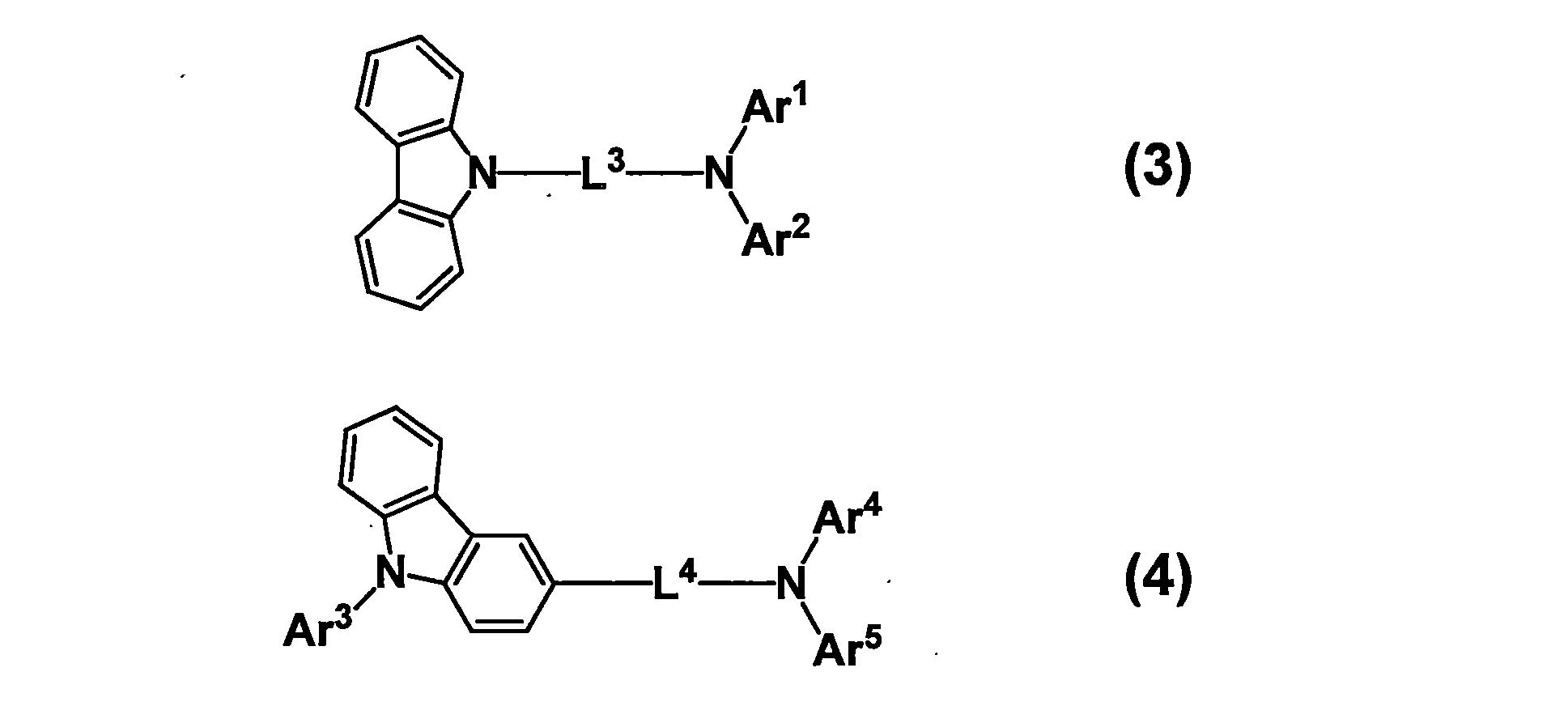
陽極と正孔輸送層の間に正孔注入層を設けてもよい。正孔注入層を設けることで発光素子が低駆動電圧化し、耐久寿命も向上する。
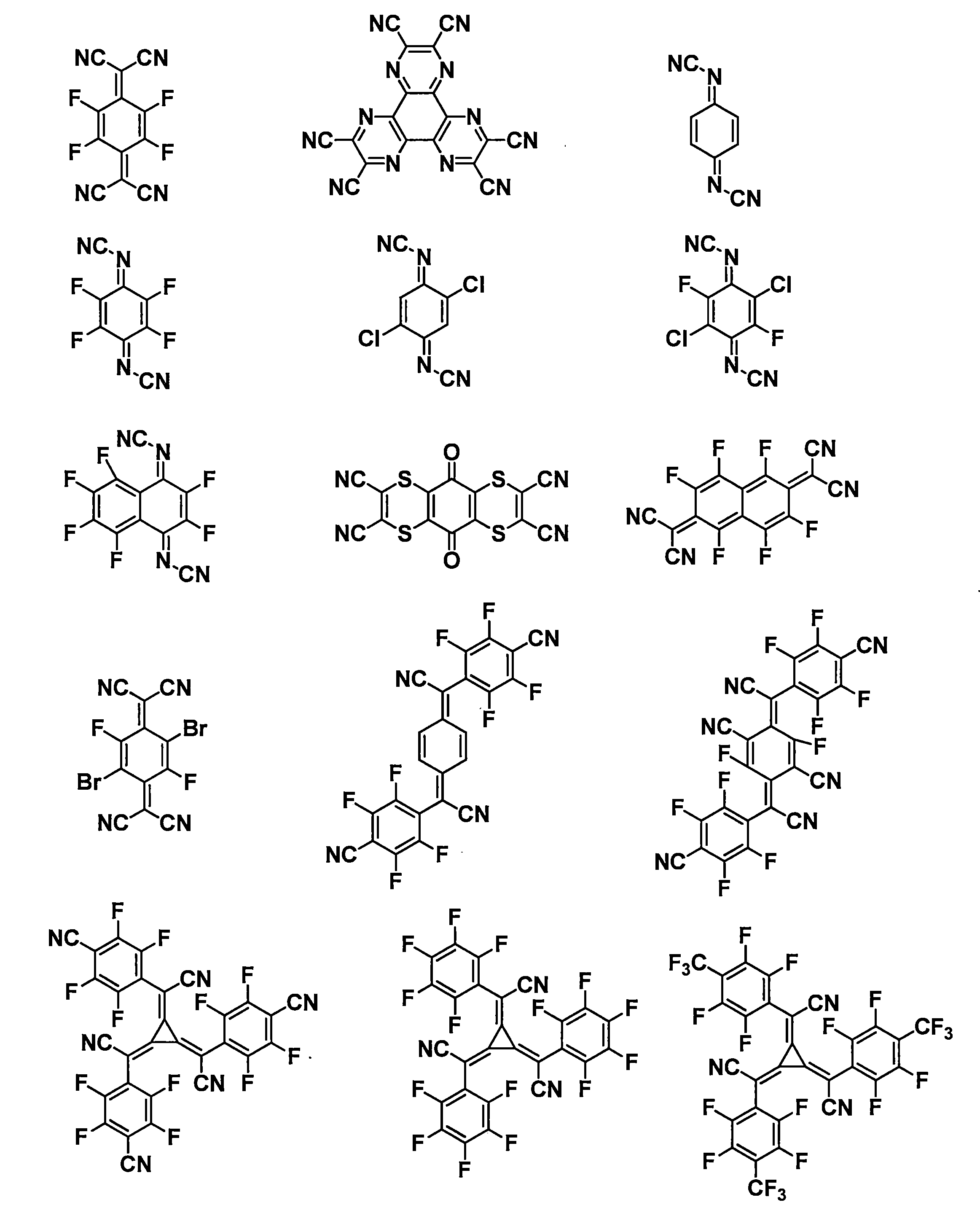
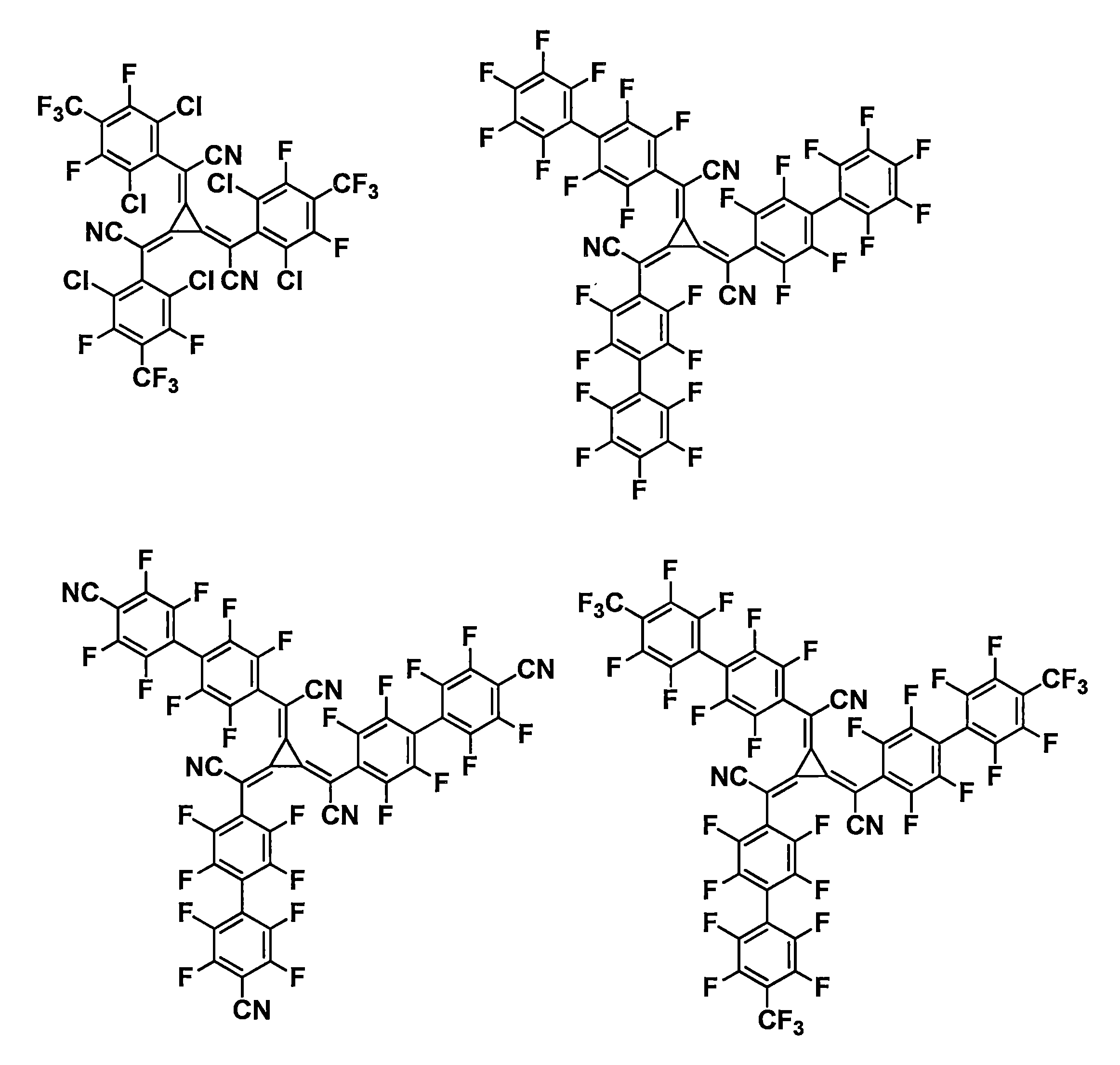
発光層は単一層、複数層のどちらでもよく、それぞれ発光材料(ホスト材料、ドーパント材料)により形成され、これはホスト材料とドーパント材料との混合物であっても、ホスト材料単独であっても、いずれでもよい。すなわち、本発明の発光素子では、各発光層において、ホスト材料もしくはドーパント材料のみが発光してもよいし、ホスト材料とドーパント材料がともに発光してもよい。電気エネルギーを効率よく利用し、高色純度の発光を得るという観点からは、発光層はホスト材料とドーパント材料の混合からなることが好ましい。
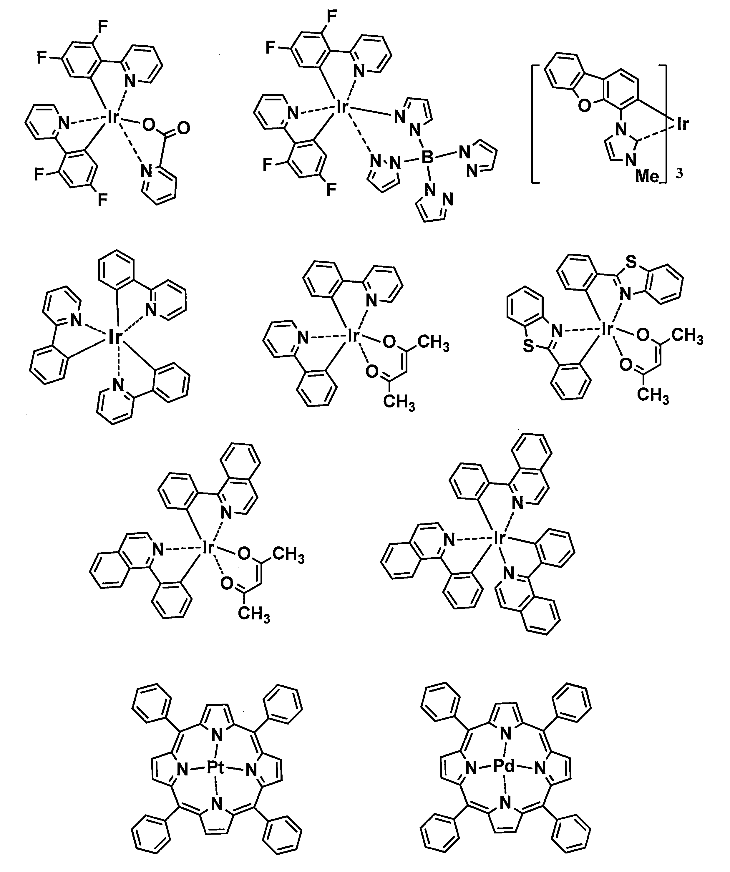
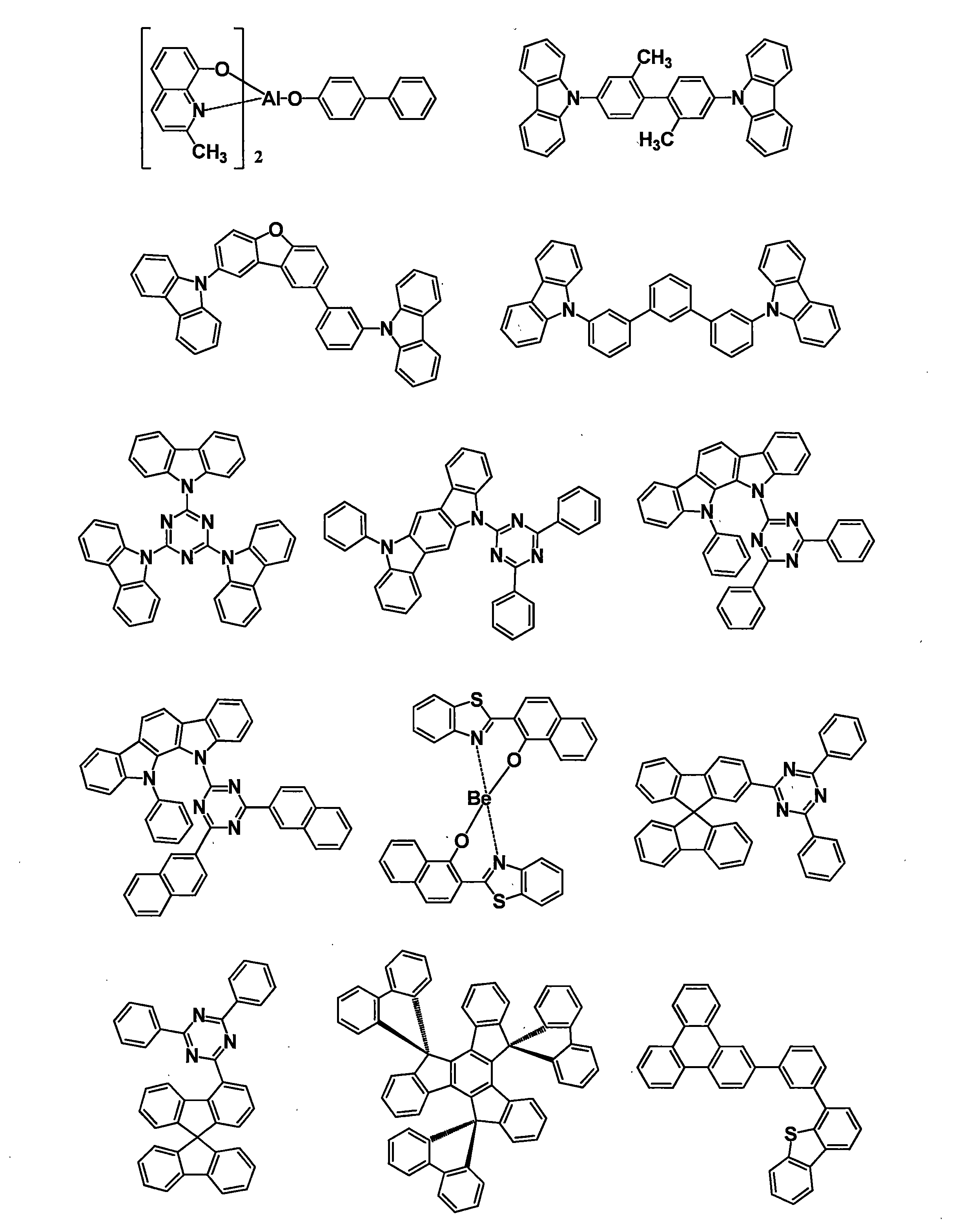
本発明において、電子輸送層とは、陰極と発光層との間にある層である。電子輸送層は単層でも複数層であってもよく、陰極もしくは発光層に接していてもいいし、接していなくてもよい。
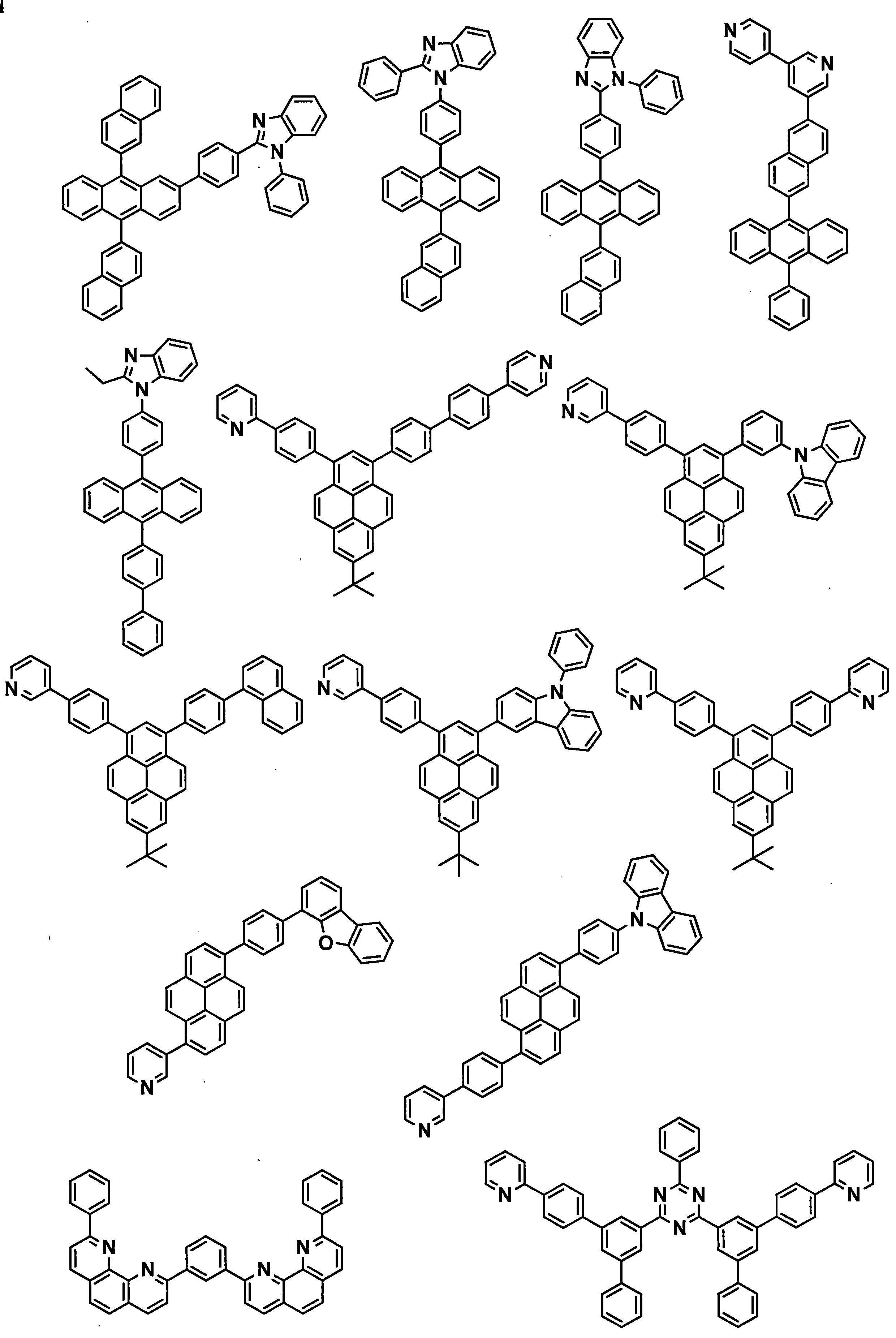
本発明において、陰極と電子輸送層の間に電子注入層を設けてもよい。一般的に電子注入層は陰極から電子輸送層への電子の注入を助ける目的で挿入されるが、挿入する場合は、電子受容性窒素を含むヘテロアリール環構造を有する化合物を用いてもよいし、上記のドナー性材料を含有する層を用いてもよい。本発明のフェナントロリン誘導体が電子注入層に含まれていてもよい。
本発明において、電荷発生層とは、上記のタンデム構造型素子における、陽極と陰極の間にある中間層であり、電荷分離により正孔および電子を発生させる層である。電荷発生層は、一般に、陰極側のP型層と陽極側のN型層から形成される。これらの層には、効率的な電荷分離と、生じたキャリアの効率的な輸送が望まれる。
化合物[A-1]の合成
2-アセチルピリジン12.1g、8-アミノキノリン-7-カルボアルデヒド17.2g、水酸化カリウム14.0g、エタノール1000mLを混合し、窒素置換した後に加熱還流した。4.5時間後、室温に冷却した後、トルエン500mL、水1000mLを加え分液した。水層をトルエン500mLで2回抽出した後、先の有機層と合わせ、エタノールを減圧留去した。溶液を硫酸マグネシウムで乾燥し、溶媒を減圧留去した後、真空乾燥することにより、中間体[a]を23.9g得た。
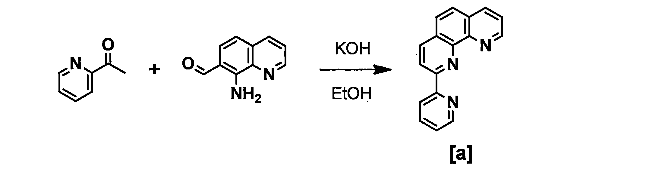


化合物[A-2]の合成
3-アセチルピリジン12.1g、8-アミノキノリン-7-カルボアルデヒド17.2g、水酸化カリウム14.0g、エタノール1000mLを混合し、窒素置換した後に加熱還流した。4.5時間後、室温に冷却した後、トルエン500mL、水1000mLを加え分液した。水層をトルエン500mLで2回抽出した後、先の有機層と合わせ、エタノールを減圧留去した。溶液を無水硫酸ナトリウムで乾燥し、溶媒を減圧留去した後、真空乾燥することにより、中間体[c]を14.4g得た。

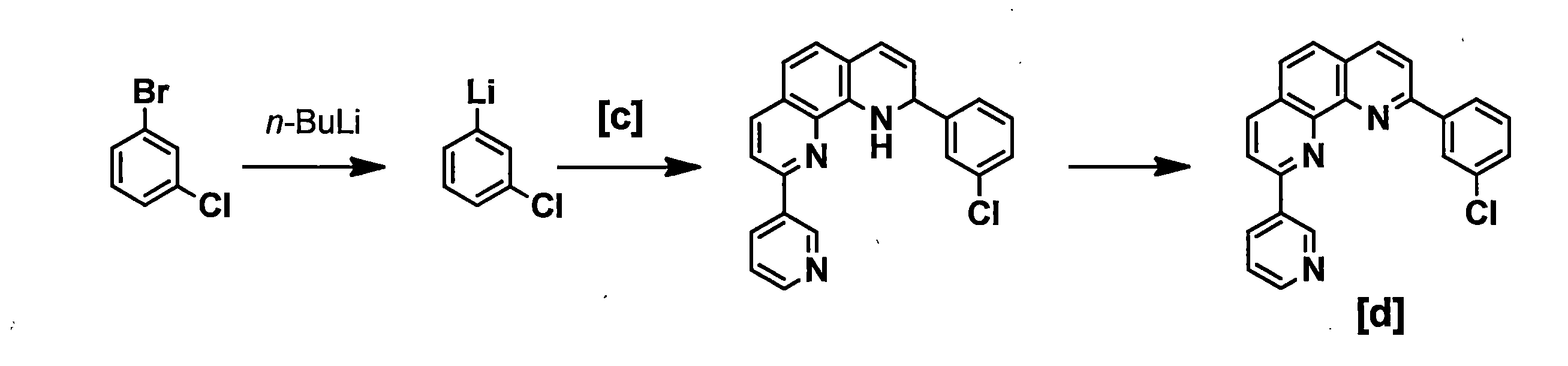
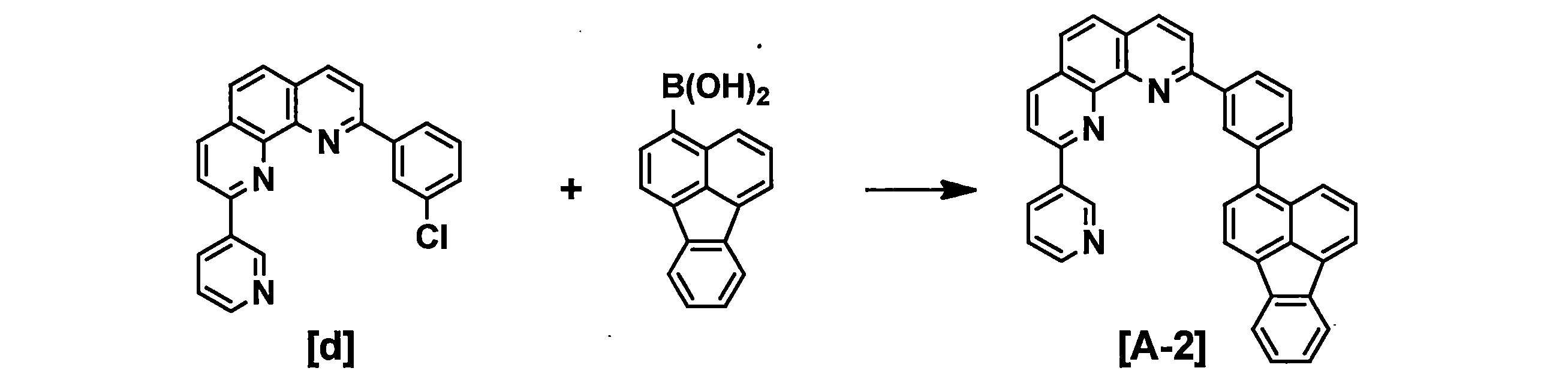
化合物[A-3]の合成
4’-クロロアセトフェノン15.5g、8-アミノキノリン-7-カルボアルデヒド17.2g、水酸化カリウム14.0g、エタノール1000mLを混合し、窒素置換した後に加熱還流した。4.5時間後、室温に冷却した後、トルエン500mL、水1000mLを加え分液した。水層をトルエン500mLで2回抽出した後、先の有機層と合わせ、エタノールを減圧留去した。溶液を無水硫酸ナトリウムで乾燥し、溶媒を減圧留去した後、真空乾燥することにより、中間体[e]を25.9g得た。




化合物[A-4]の合成
中間体[e]8.20g、3-フルオランテンボロン酸6.80g、1,4-ジオキサン282.0mL、1.27Mリン酸カリウム水溶液48.9mLを混合し、窒素置換した。この混合溶液にビス(ジベンジリデンアセトン)パラジウム(0)578mg、トリシクロヘキシルホスフィン・テトラフルオロボラン555mgを加え、2時間加熱還流した。室温に冷却した後、水300mlを加え、析出物をろ過した。真空乾燥後、テトラヒドロフラン800mLを加えて溶解し、活性炭1.29mgを加え、1時間加熱還流した。冷却後、シリカパットでろ過した。ろ液の溶媒を留去した後、得られた固体をピリジン/メタノールで再結晶した。得られた固体をろ過し、真空乾燥することにより、中間体[h]を10.9g得た。

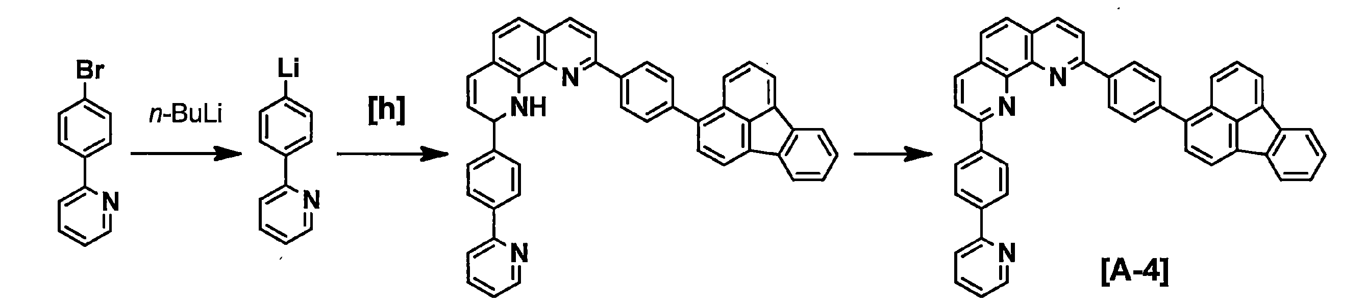
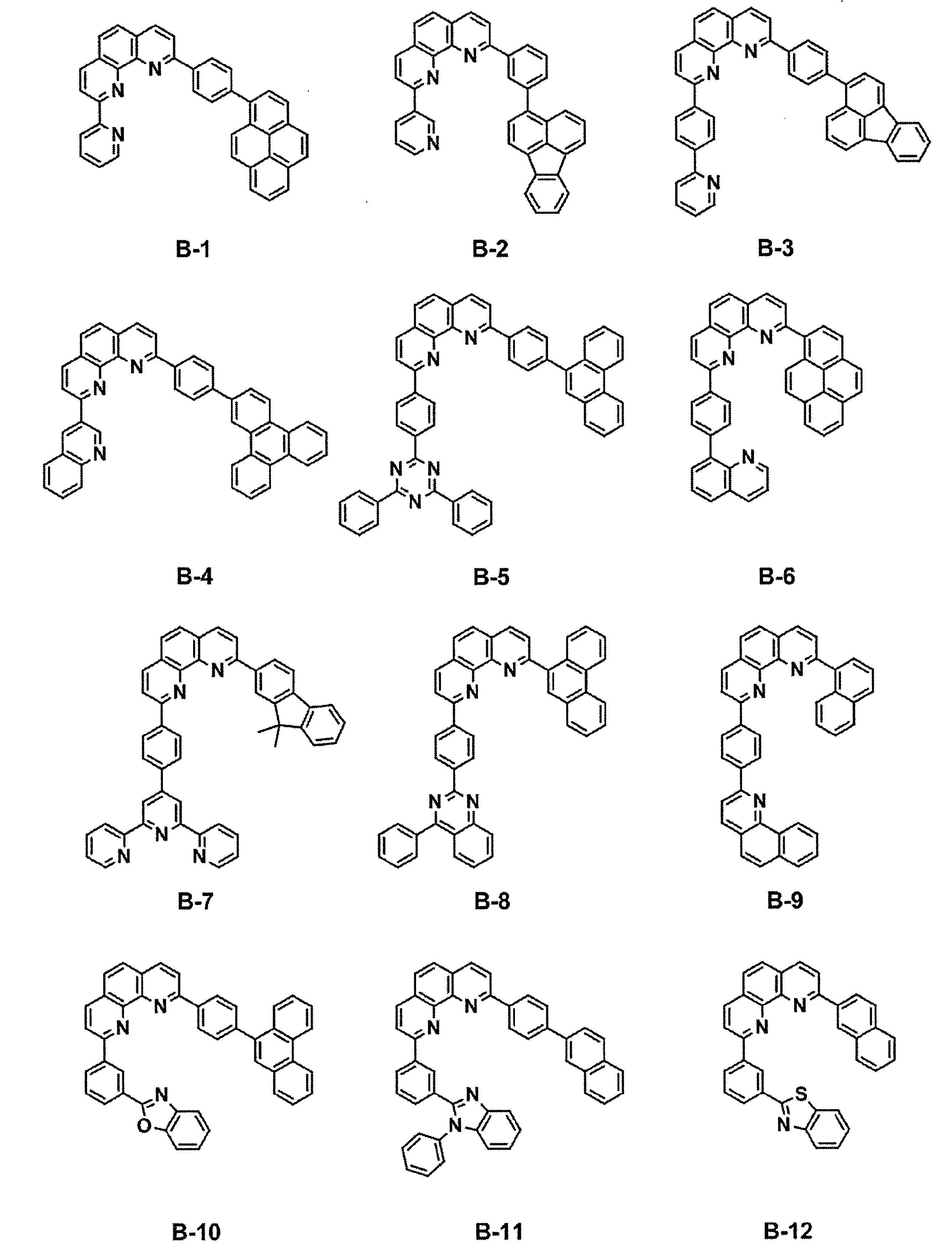
ITO透明導電膜を165nm堆積させたガラス基板(ジオマテック(株)製、11Ω/□、スパッタ品)を38×46mmに切断し、エッチングを行った。得られた基板を “セミコクリーン56”(商品名、フルウチ化学(株)製)で15分間超音波洗浄してから、超純水で洗浄した。この基板を素子を作製する直前に1時間UV-オゾン処理し、真空蒸着装置内に設置して、装置内の真空度が5×10⁻⁴Pa以下になるまで排気した。抵抗加熱法によって、まず正孔注入層として、HAT-CN6を5nm、正孔輸送層として、HT-1を50nm蒸着した。次に、発光層として、ホスト材料H-1、ドーパント材料D-1をドープ濃度が5重量%になるようにして20nmの厚さに蒸着した。次に、電子輸送層として化合物B-1を35nmの厚さに蒸着して積層した。次に、フッ化リチウムを0.5nm蒸着した後、アルミニウムを1000nm蒸着して陰極とし、5×5mm角の素子を作製した。ここで言う膜厚は、水晶発振式膜厚モニター表示値である。この発光素子の1000cd/m2時の特性は、駆動電圧4.3V、外部量子効率4.8%であった。また初期輝度を1000cd/m2に設定し、定電流駆動させたところ輝度20%低下する時間は1500時間であった。なお化合物HAT-CN6、HT-1、H-1、D-1は以下に示す化合物である。
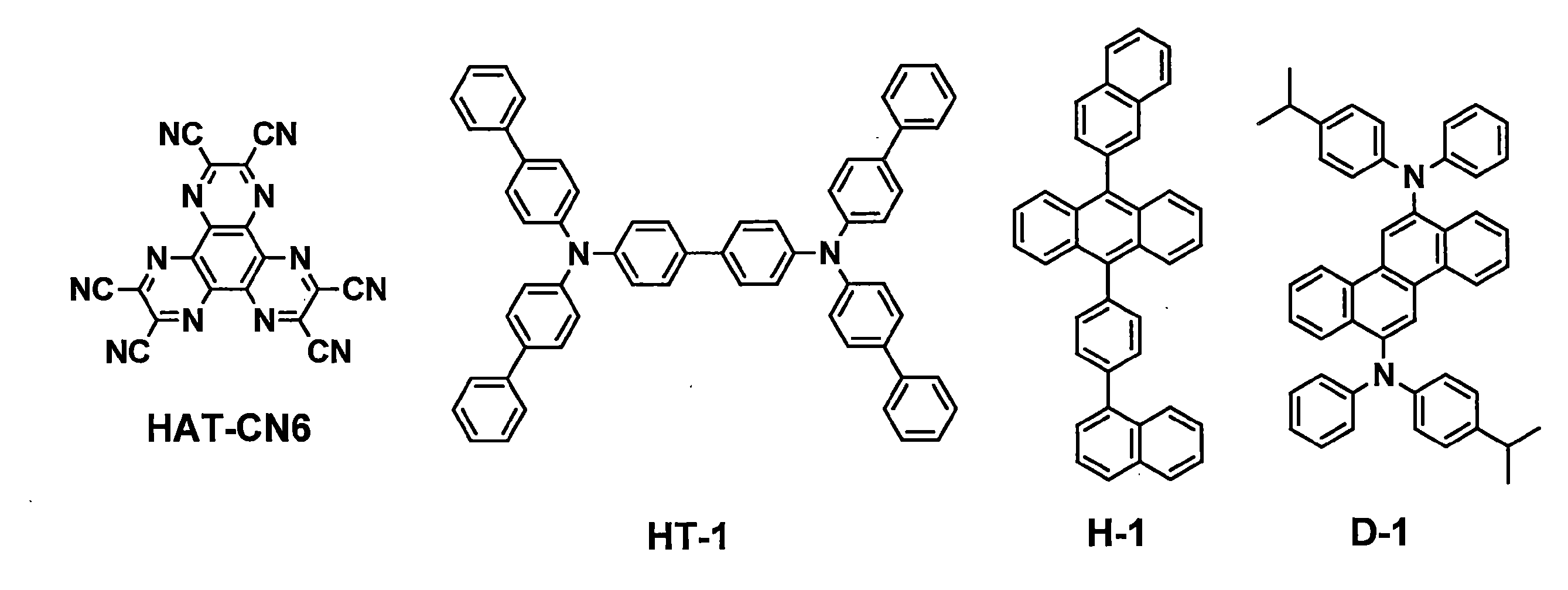
電子輸送層に表1に記載した化合物を用いた以外は実施例1と同様にして発光素子を作製し、評価した。結果を表1に示す。
電子輸送層に表1に記載した化合物を用いた以外は実施例1と同様にして発光素子を作製し、評価した。結果を表1に示す。なお、E-1~E-5は以下に示す化合物である。

ITO透明導電膜を165nm堆積させたガラス基板(ジオマテック(株)製、11Ω/□、スパッタ品)を38×46mmに切断し、エッチングを行った。得られた基板を “セミコクリーン56”(商品名、フルウチ化学(株)製)で15分間超音波洗浄してから、超純水で洗浄した。この基板を素子を作製する直前に1時間UV-オゾン処理し、真空蒸着装置内に設置して、装置内の真空度が5×10⁻⁴Pa以下になるまで排気した。抵抗加熱法によって、まず正孔注入層として、HAT-CN6を5nm、正孔輸送層として、HT-1を50nm蒸着した。次に、発光層として、ホスト材料H-1、ドーパント材料D-1をドープ濃度が5重量%になるようにして20nmの厚さに蒸着した。次に、第1電子輸送層として化合物B-1を25nmの厚さに蒸着して積層した。さらに第2電子輸送層として電子輸送材料に化合物B-1を、ドナー性材料としてリチウムを用い、化合物B-1とリチウムの蒸着速度比が20:1になるようにして10nmの厚さに積層した。次に、フッ化リチウムを0.5nm蒸着した後、アルミニウムを1000nm蒸着して陰極とし、5×5mm角の素子を作製した。この発光素子の1000cd/m2時の特性は、駆動電圧3.9V、外部量子効率5.8%であった。また初期輝度を1000cd/m2に設定し、定電流駆動させたところ輝度20%低下する時間は1650時間であった。
電子輸送層に表2に記載した化合物を用いた以外は実施例13と同様にして発光素子を作製し、評価した。結果を表2に示す。
電子輸送層に表2に記載した化合物を用いた以外は実施例13と同様にして発光素子を作製し、評価した。結果を表2に示す。
ITO透明導電膜を165nm堆積させたガラス基板(ジオマテック(株)製、11Ω/□、スパッタ品)を38×46mmに切断し、エッチングを行った。得られた基板を “セミコクリーン56”(商品名、フルウチ化学(株)製)で15分間超音波洗浄してから、超純水で洗浄した。この基板を素子を作製する直前に1時間UV-オゾン処理し、真空蒸着装置内に設置して、装置内の真空度が5×10⁻⁴Pa以下になるまで排気した。抵抗加熱法によって、まず正孔注入層として、HAT-CN6を5nm、正孔輸送層として、HT-1を50nm蒸着した。次に、発光層として、ホスト材料H-1、ドーパント材料D-1をドープ濃度が5重量%になるようにして20nmの厚さに蒸着した。さらに電子輸送層として電子輸送材料に化合物B-1を、ドナー性材料として2E-1を用い、化合物B-1と2E-1の蒸着速度比が1:1になるようにして35nmの厚さに積層した。この電子輸送層は表4では第2電子輸送層として示す。次に、フッ化リチウムを0.5nm蒸着した後、マグネシウムと銀を1000nm共蒸着して陰極とし、5×5mm角の素子を作製した。この発光素子の1000cd/m2時の特性は、駆動電圧3.9V、外部量子効率6.0%であった。また初期輝度を1000cd/m2に設定し、定電流駆動させたところ輝度20%低下する時間は1800時間であった。なお、2E-1は下記に示す化合物である。
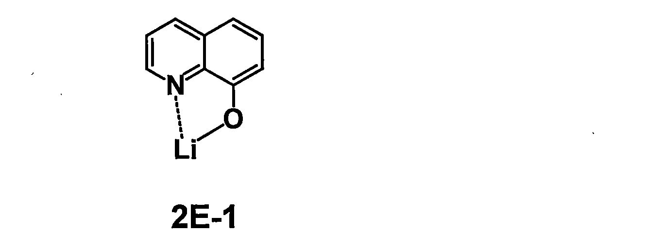
電子輸送層、ドナー性材料として表3に記載した化合物を用いた以外は実施例25と同様にして発光素子を作製し、評価した。結果を表3に示す。
電子輸送層、ドナー性材料として表3に記載した化合物を用いた以外は実施例25と同様にして発光素子を作製し、評価した。結果を表3に示す。
第1電子輸送層として化合物B-1を25nmの厚さに蒸着して積層し、さらに第2電子輸送層として電子輸送材料に化合物B-1を、ドナー性材料として2E-1を用い、化合物B-1と2E-1の蒸着速度比が1:1になるようにして10nmの厚さに積層した。それ以外は実施例25と同様にして発光素子を作製した。この発光素子の1000cd/m2時の特性は、駆動電圧4.0V、外部量子効率5.9%であった。また初期輝度を1000cd/m2に設定し、定電流駆動させたところ輝度20%低下する時間は1950時間であった。
電子輸送層、ドナー性材料として表4に記載した化合物を用いた以外は実施例37と同様にして発光素子を作製し、評価した。結果を表4に示す。
電子輸送層、ドナー性材料として表4に記載した化合物を用いた以外は実施例37と同様にして発光素子を作製し、評価した。結果を表4に示す。
ITO透明導電膜を165nm堆積させたガラス基板(ジオマテック(株)製、11Ω/□、スパッタ品)を38×46mmに切断し、エッチングを行った。得られた基板を “セミコクリーン56”(商品名、フルウチ化学(株)製)で15分間超音波洗浄してから、超純水で洗浄した。この基板を素子を作製する直前に1時間UV-オゾン処理し、真空蒸着装置内に設置して、装置内の真空度が5×10⁻⁴Pa以下になるまで排気した。抵抗加熱法によって、まず正孔注入層として、HAT-CN6を5nm、正孔輸送層として、HT-1を50nm蒸着した。この正孔輸送層は表6では第1正孔輸送層として示す。次に、発光層として、ホスト材料H-2、ドーパント材料D-2をドープ濃度が10重量%になるようにして20nmの厚さに蒸着した。次に、電子輸送層として化合物B-2を35nmの厚さに蒸着して積層した。次に、フッ化リチウムを0.5nm蒸着した後、アルミニウムを1000nm蒸着して陰極とし、5×5mm角の素子を作製した。ここで言う膜厚は、水晶発振式膜厚モニター表示値である。この発光素子の4000cd/m2時の特性は、駆動電圧3.9V、外部量子効率10.4%であった。また初期輝度を4000cd/m2に設定し、定電流駆動させたところ輝度20%低下する時間は1400時間であった。なおH-2、D-2は以下に示す化合物である。
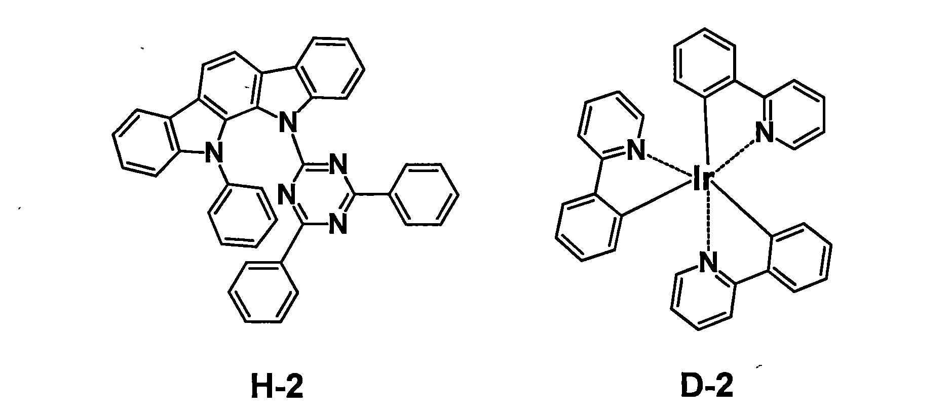
電子輸送層として表5記載の化合物を用いた以外は実施例49と同様に発光素子を作製し、評価した。結果を表5に示す。
電子輸送層として表5記載の化合物を用いた以外は実施例49と同様に発光素子を作製し、評価した。結果を表5に示す。
ITO透明導電膜を165nm堆積させたガラス基板(ジオマテック(株)製、11Ω/□、スパッタ品)を38×46mmに切断し、エッチングを行った。得られた基板を “セミコクリーン56”(商品名、フルウチ化学(株)製)で15分間超音波洗浄してから、超純水で洗浄した。この基板を素子を作製する直前に1時間UV-オゾン処理し、真空蒸着装置内に設置して、装置内の真空度が5×10⁻⁴Pa以下になるまで排気した。抵抗加熱法によって、まず正孔注入層として、HAT-CN6を5nm、第1正孔輸送層として、HT-1を40nm蒸着した。さらに第2正孔輸送層としてHT-2を10nm蒸着した。次に、発光層として、ホスト材料H-2、ドーパント材料D-2をドープ濃度が10重量%になるようにして20nmの厚さに蒸着した。次に、電子輸送層として化合物B-2を35nmの厚さに蒸着して積層した。次に、フッ化リチウムを0.5nm蒸着した後、アルミニウムを1000nm蒸着して陰極とし、5×5mm角の素子を作製した。ここで言う膜厚は、水晶発振式膜厚モニター表示値である。この発光素子の4000cd/m2時の特性は、駆動電圧3.9V、外部量子効率13.3%であった。また初期輝度を4000cd/m2に設定し、定電流駆動させたところ輝度20%低下する時間は1600時間であった。なお、HT-2は以下に示す化合物である。
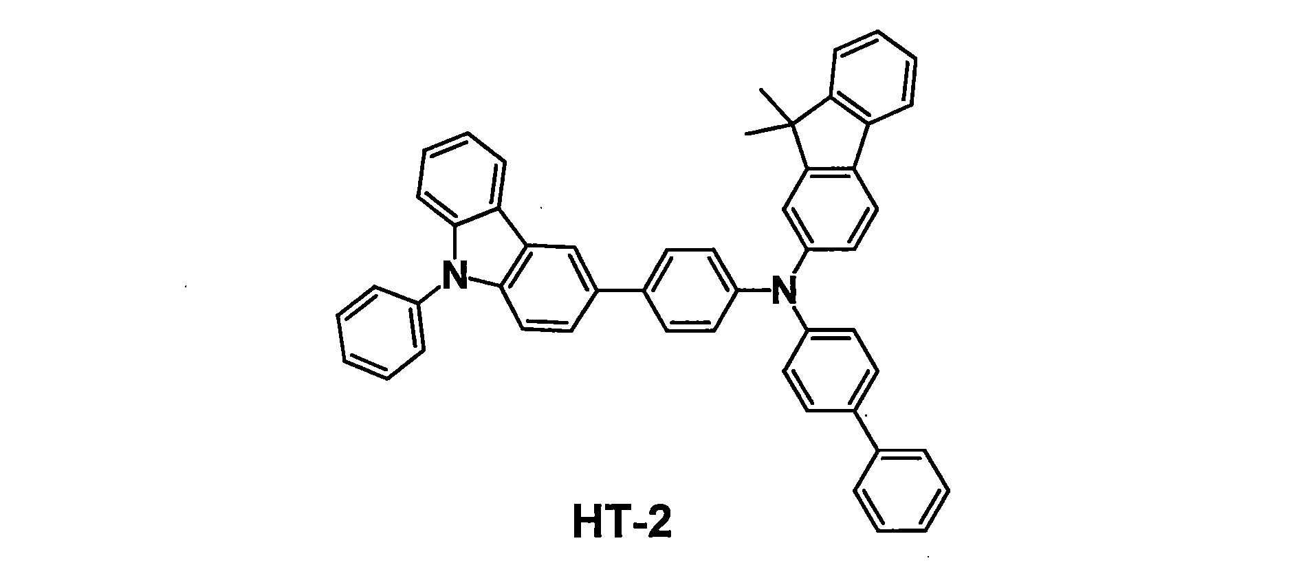
第2正孔輸送層および電子輸送層として表5記載の化合物を用いた以外は、実施例55と同様にして素子を作製し、評価した。結果を表5に示す。なおHT-3、HT-4、HT-5は以下に示す化合物である。

第2正孔輸送層および電子輸送層として表5記載の化合物を用いた以外は、実施例55と同様にして素子を作製し、評価した。結果を表5に示す。
ITO透明導電膜を165nm堆積させたガラス基板(ジオマテック(株)製、11Ω/□、スパッタ品)を38×46mmに切断し、エッチングを行った。得られた基板を “セミコクリーン56”(商品名、フルウチ化学(株)製)で15分間超音波洗浄してから、超純水で洗浄した。この基板を素子を作製する直前に1時間UV-オゾン処理し、真空蒸着装置内に設置して、装置内の真空度が5×10-4Pa以下になるまで排気した。抵抗加熱法によって、まず正孔注入層として、HAT-CN6を10nm、正孔輸送層として、HT-6を90nm蒸着した。次に、発光層として、ホスト材料H-1、ドーパント材料D-3をドープ濃度が5重量%になるようにして30nmの厚さに蒸着し、その上に、電子輸送層として化合物ET-1を30nmの厚さに蒸着して積層した。次にN型の電荷発生層として電子輸送材料に化合物B-1を、ドナー性材料としてリチウムを用い、化合物B-1とリチウムの蒸着速度比が20:1になるようにして10nmの厚さに積層し、その上に、P型の電荷発生層として、HT-6を10nm蒸着した。さらに、正孔注入層、正孔輸送層、発光層、電子輸送層を上記と同様の条件で積層した後、フッ化リチウムを0.5nm蒸着した後、アルミニウムを1000nm蒸着して陰極とし、5×5mm角の素子を作製した。この発光素子の1000cd/m2時の特性は、駆動電圧8.7V、外部量子効率6.9%であった。また初期輝度を1000cd/m2に設定し、定電流駆動させたところ輝度20%低下する時間は1000時間であった。なおHT-6、ET-1、D-3は以下に示す化合物である。
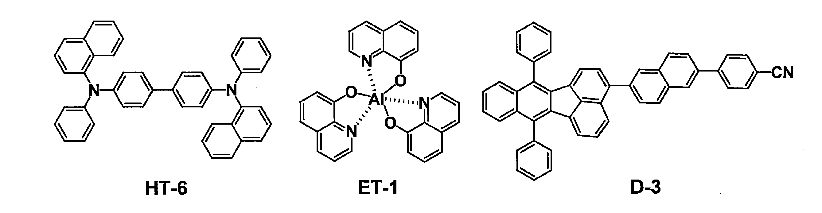
N型の電荷発生層の電子輸送材料として表6記載の化合物を用いた以外は、実施例70と同様にして素子を作製し、評価した。結果を表6に示す。
N型の電荷発生層の電子輸送材料として表6記載の化合物を用いた以外は、実施例70と同様にして素子を作製し、評価した。結果を表6に示す。


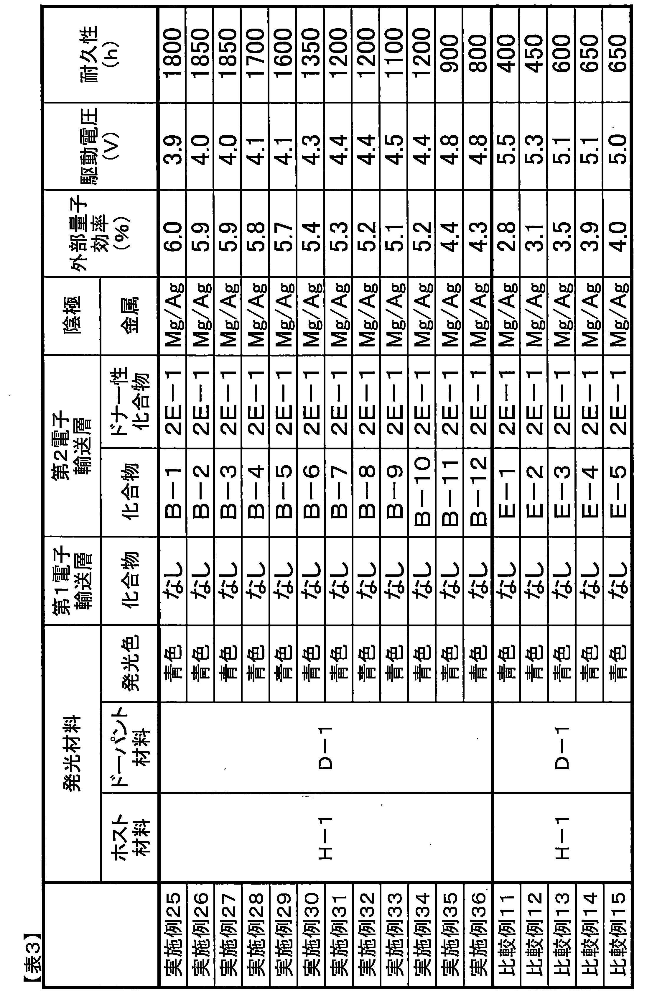

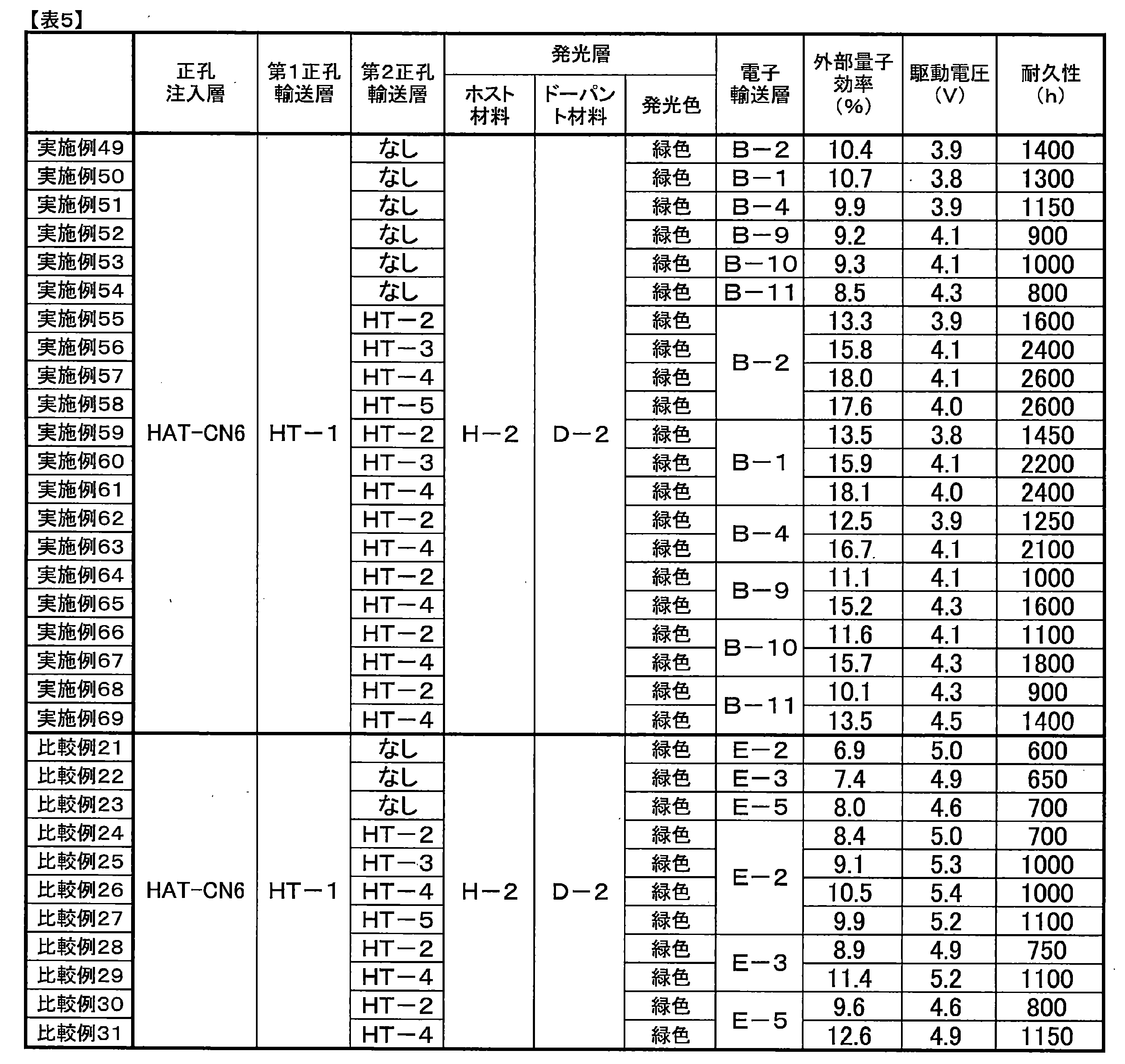

Claims (15)
- 下記一般式(1)で表されるフェナントロリン誘導体。
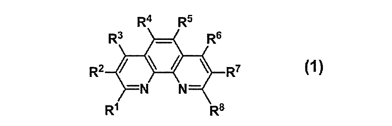
L1およびL2はそれぞれ同じでも異なっていてもよく、単結合またはフェニレン基のいずれかから選ばれる。
Bは電子受容性窒素を有する置換もしくは無置換のヘテロアリール基、Cは置換もしくは無置換の環形成炭素数が20未満であるアリール基を表す。ただし、Bはフェナントロリン骨格を有さない。
BおよびCが置換される場合、置換基としては、重水素、アルキル基、シクロアルキル基、複素環基、アルケニル基、シクロアルケニル基、アルキニル基、アルコキシ基、アルキルチオ基、アリールエーテル基、アリールチオエーテル基、ハロゲン、シアノ基、カルボニル基、カルボキシル基、オキシカルボニル基、カルバモイル基、アミノ基、ボリル基、シリル基、フェニル基、ナフチル基、ピリジル基、キノリニル基および-P(=O)R9R10からなる群より選ばれる。これらの基は、さらに重水素、アルキル基、ハロゲン、フェニル基、ナフチル基、ピリジル基またはキノリニル基で置換されていても良い。) - R1がL1-Bで表される基であり、かつ、R8がL2-Cで表される基である請求項1に記載のフェナントロリン誘導体。
- L2がフェニレン基である請求項1または2に記載のフェナントロリン誘導体。
- Cがフルオレニル基、フェナントレニル基、ピレニル基、トリフェニレニル基またはフルオランテニル基である請求項1~3のいずれかに記載のフェナントロリン誘導体。
- Cがピレニル基またはフルオランテニル基である請求項1~4のいずれかに記載のフェナントロリン誘導体。
- Bがピリジル基、キノリニル基、イソキノリニル基、ピラジニル基、ピリミジニル基、ピリダジニル基、トリアジニル基、キノキサリニル基、キナゾリニル基、ベンゾキノリニル基、アクリジニル基、ベンゾイミダゾリル基またはイミダゾピリジル基である請求項1~5のいずれかに記載のフェナントロリン誘導体。
- Bがピリジル基、キノリニル基またはイソキノリニル基である請求項1~6のいずれかに記載のフェナントロリン誘導体。
- 陽極と陰極の間に発光層を含む複数の有機層を有し、電気エネルギーにより発光する発光素子であって、前記有機層の少なくとも1層に請求項1~7のいずれかに記載のフェナントロリン誘導体を含む発光素子。
- 前記有機層に少なくとも電子輸送層が存在し、電子輸送層が請求項1~7いずれかに記載のフェナントロリン誘導体を含む請求項8記載の発光素子。
- 前記有機層に少なくとも電子注入層が存在し、電子注入層が請求項1~7いずれかに記載のフェナントロリン誘導体を含む請求項8または9に記載の発光素子。
- 前記有機層に少なくとも電荷発生層が存在し、電荷発生層が請求項1~7いずれかに記載のフェナントロリン誘導体を含むことを特徴とする請求項8~10のいずれかに記載の発光素子。
- 第一電極及び第二電極の間に少なくとも一層の有機層があり、光エネルギーを電気エネルギーに変換する光電変換素子であって、前記有機層に請求項1~7のいずれかに記載のフェナントロリン誘導体を含む光電変換素子。
- 前記有機層が光電変換層を含み、該光電変換層に前記有機層に請求項1~7のいずれかに記載のフェナントロリン誘導体を含む請求項12に記載の光電変換素子。
- 前記有機層が、第一電極及び第二電極の間に少なくとも一層の光電変換層と一層の電子取り出し層を含み、該電子取り出し層が前記有機層に請求項1~7のいずれかに記載のフェナントロリン誘導体を含む請求項12または13に記載の光電変換素子。
- 請求項12~14のいずれかに記載の光電変換素子を含むイメージセンサ。
Priority Applications (5)
| Application Number | Priority Date | Filing Date | Title |
|---|---|---|---|
| KR1020177021762A KR102214158B1 (ko) | 2015-01-29 | 2016-01-20 | 페난트롤린 유도체, 그것을 함유하는 전자 디바이스, 발광 소자 및 광전 변환 소자 |
| CN201680007064.1A CN107207503A (zh) | 2015-01-29 | 2016-01-20 | 菲咯啉衍生物、含有其的电子装置、发光元件及光电转换元件 |
| JP2016503865A JP6769303B2 (ja) | 2015-01-29 | 2016-01-20 | フェナントロリン誘導体、それを含有する電子デバイス、発光素子および光電変換素子 |
| EP16743201.2A EP3252052B1 (en) | 2015-01-29 | 2016-01-20 | Phenanthroline derivative, electronic device containing same, light emitting element, and photoelectric conversion element |
| US15/544,719 US20180019407A1 (en) | 2015-01-29 | 2016-01-20 | Phenanthroline derivative, electronic device containing same, light emitting element, and photoelectric conversion element |
Applications Claiming Priority (2)
| Application Number | Priority Date | Filing Date | Title |
|---|---|---|---|
| JP2015015452 | 2015-01-29 | ||
| JP2015-015452 | 2015-01-29 |
Publications (1)
| Publication Number | Publication Date |
|---|---|
| WO2016121597A1 true WO2016121597A1 (ja) | 2016-08-04 |
Family
ID=56543212
Family Applications (1)
| Application Number | Title | Priority Date | Filing Date |
|---|---|---|---|
| PCT/JP2016/051578 Ceased WO2016121597A1 (ja) | 2015-01-29 | 2016-01-20 | フェナントロリン誘導体、それを含有する電子デバイス、発光素子および光電変換素子 |
Country Status (7)
| Country | Link |
|---|---|
| US (1) | US20180019407A1 (ja) |
| EP (1) | EP3252052B1 (ja) |
| JP (1) | JP6769303B2 (ja) |
| KR (1) | KR102214158B1 (ja) |
| CN (1) | CN107207503A (ja) |
| TW (1) | TWI680130B (ja) |
| WO (1) | WO2016121597A1 (ja) |
Cited By (16)
| Publication number | Priority date | Publication date | Assignee | Title |
|---|---|---|---|---|
| CN106831766A (zh) * | 2016-12-28 | 2017-06-13 | 陕西莱特光电材料股份有限公司 | 一种新型双极性发光主体材料及其合成方法与应用 |
| EP3263570A1 (en) * | 2016-06-30 | 2018-01-03 | LG Display Co., Ltd. | Organic compound, and organic light emitting diode and organic light emitting display device including the same |
| WO2018105776A1 (ko) * | 2016-12-07 | 2018-06-14 | 주식회사 진웅산업 | 페난스롤린 화합물 및 이를 포함하는 유기발광소자 |
| CN109119541A (zh) * | 2017-06-26 | 2019-01-01 | 东丽先端材料研究开发(中国)有限公司 | 量子点发光元件 |
| JP2019192557A (ja) * | 2018-04-26 | 2019-10-31 | キヤノン株式会社 | 有機el素子、それを有する表示装置、撮像装置、照明装置、移動体 |
| US10903432B2 (en) | 2017-08-08 | 2021-01-26 | Samsung Display Co., Ltd. | Heterocyclic compound and organic light-emitting device including the same |
| JP2021155351A (ja) * | 2020-03-26 | 2021-10-07 | 東レ株式会社 | フェナントロリン誘導体の結晶およびその製造方法 |
| JP2021166281A (ja) * | 2020-04-03 | 2021-10-14 | 日本放送協会 | 有機薄膜及び有機薄膜の製造方法、有機エレクトロルミネッセンス素子、表示装置、照明装置、有機薄膜太陽電池、光電変換素子、薄膜トランジスタ、塗料組成物、並びに、有機エレクトロルミネッセンス素子用材料 |
| JP2022115839A (ja) * | 2021-01-28 | 2022-08-09 | ケミプロ化成株式会社 | 新規な1,10-フェナントロリン化合物を用いた有機エレクトロルミネッセンス素子、及び有機エレクトロルミネッセンス照明 |
| US11563183B2 (en) | 2017-06-21 | 2023-01-24 | Samsung Display Co., Ltd. | Heterocyclic compound and organic light-emitting device including the same |
| US11588111B2 (en) | 2017-08-04 | 2023-02-21 | Samsung Display Co., Ltd. | Condensed-cyclic compound and organic light-emitting device including the same |
| WO2023058644A1 (ja) * | 2021-10-08 | 2023-04-13 | 東レ株式会社 | 化合物、有機el素子、表示装置および照明装置 |
| WO2023190159A1 (ja) * | 2022-04-01 | 2023-10-05 | 東レ株式会社 | 化合物、それを用いた発光素子材料および発光素子、光電変換素子材料、色変換組成物、色変換シート、光源ユニット、表示装置、照明装置 |
| KR20230151982A (ko) | 2021-02-24 | 2023-11-02 | 도레이 카부시키가이샤 | 유기 el 소자용 재료, 유기 el 소자, 표시 장치 및조명 장치 |
| WO2024043018A1 (ja) * | 2022-08-22 | 2024-02-29 | 東レ株式会社 | 有機el素子、表示装置および照明装置 |
| US12084433B2 (en) | 2018-03-23 | 2024-09-10 | Samsung Display Co., Ltd. | Heterocyclic compound and organic light-emitting device including the same |
Families Citing this family (23)
| Publication number | Priority date | Publication date | Assignee | Title |
|---|---|---|---|---|
| GB2545626A (en) * | 2015-10-16 | 2017-06-28 | Lomox Ltd | Cross-linkable charge transport materials |
| KR102157756B1 (ko) * | 2016-12-12 | 2020-09-18 | 엘지디스플레이 주식회사 | 유기 화합물과 이를 포함하는 유기발광다이오드 및 유기발광 표시장치 |
| TWI618093B (zh) * | 2016-12-14 | 2018-03-11 | 行政院原子能委員會核能研究所 | 具備高熱穩定性效能之有機太陽能電池之製備方法 |
| US20200127039A1 (en) * | 2017-01-24 | 2020-04-23 | Sony Semiconductor Solutions Corporation | Light-receiving device, method of manufacturing light receiving device, imaging device, and electronic apparatus |
| CN107602553B (zh) * | 2017-07-31 | 2020-11-24 | 华南理工大学 | 有机小分子电子传输材料及其制备方法与应用 |
| KR102206995B1 (ko) * | 2017-12-13 | 2021-01-22 | 엘지디스플레이 주식회사 | 유기 화합물과 이를 포함하는 유기발광다이오드 및 유기발광 표시장치 |
| KR102486441B1 (ko) * | 2017-12-28 | 2023-01-06 | 엘지디스플레이 주식회사 | 유기발광다이오드 |
| KR102239793B1 (ko) * | 2019-04-25 | 2021-04-13 | 주식회사 진웅산업 | 페난트롤린 화합물 및 이를 포함하는 유기발광소자 |
| EP3799143B1 (en) * | 2019-09-26 | 2024-09-11 | Novaled GmbH | First and second organic semiconductor layer and organic electronic device comprising the same |
| KR102822445B1 (ko) * | 2019-12-31 | 2025-06-19 | 엘지디스플레이 주식회사 | 유기전기소자, 이를 포함하는 표시패널 및 이를 포함하는 표시장치 |
| KR20210115282A (ko) * | 2020-03-12 | 2021-09-27 | 에스에프씨 주식회사 | 신규한 페난트롤린계 화합물 및 이를 포함하는 유기 발광 소자 |
| KR102875347B1 (ko) * | 2020-03-26 | 2025-10-24 | 도레이 카부시키가이샤 | 페난트롤린 유도체의 결정 및 그 제조 방법, 그리고 그것을 사용한 발광 소자 |
| KR20220076881A (ko) | 2020-12-01 | 2022-06-08 | 엘지디스플레이 주식회사 | 유기 화합물, 이를 포함하는 유기발광다이오드 및 유기발광장치 |
| KR20230108808A (ko) * | 2022-01-11 | 2023-07-19 | 삼성디스플레이 주식회사 | 발광 소자 및 상기 발광 소자를 포함한 전자 장치 |
| KR102625989B1 (ko) * | 2022-02-08 | 2024-01-18 | 광주과학기술원 | 신규 페난스롤린계 화합물, 이의 제조방법 및 이를 패시베이션층으로 포함하는 광전자 소자 |
| CN114315871B (zh) * | 2022-03-10 | 2022-06-28 | 浙江华显光电科技有限公司 | 邻菲啰啉化合物、有机电致发光器件及显示或照明装置 |
| CN114573579B (zh) * | 2022-03-10 | 2024-06-18 | 宇瑞(上海)化学有限公司 | 邻菲啰啉化合物、有机电致发光器件及显示或照明装置 |
| CN114621257B (zh) * | 2022-03-31 | 2024-07-05 | 宇瑞(上海)化学有限公司 | 邻菲啰啉化合物、有机电致发光器件及显示或照明装置 |
| CN114874208B (zh) * | 2022-04-20 | 2024-04-26 | 宇瑞(上海)化学有限公司 | 邻菲啰啉化合物、有机电致发光器件及显示或照明装置 |
| CN115141216B (zh) * | 2022-07-25 | 2024-03-12 | 宇瑞(上海)化学有限公司 | 一种含嗪类化合物及其有机发光器件 |
| KR20250063264A (ko) * | 2023-10-31 | 2025-05-08 | 주식회사 진웅산업 | 신규 화합물 및 이를 포함하는 유기 발광 소자 |
| KR20250090182A (ko) | 2023-12-12 | 2025-06-19 | 듀폰스페셜티머터리얼스코리아 유한회사 | 화합물 및 이를 포함하는 유기 전계 발광 소자 |
| CN118619949B (zh) * | 2024-07-02 | 2025-02-07 | 浙江华显光电科技有限公司 | 一种含有苯并五元氮杂环的菲啰啉化合物、有机电致发光器件及显示或照明装置 |
Citations (9)
| Publication number | Priority date | Publication date | Assignee | Title |
|---|---|---|---|---|
| JP2005108720A (ja) * | 2003-09-30 | 2005-04-21 | Tdk Corp | 有機el素子用化合物および有機el素子 |
| JP2008189660A (ja) * | 2007-01-11 | 2008-08-21 | Toray Ind Inc | 含窒素芳香環誘導体の製造方法 |
| CN102127073A (zh) * | 2010-11-26 | 2011-07-20 | 深圳大学 | 以邻菲罗啉为核心的星状化合物及具该化合物的发光器件 |
| CN102372709A (zh) * | 2010-08-20 | 2012-03-14 | 清华大学 | 一种芳基菲咯啉类化合物及应用 |
| KR20120072785A (ko) * | 2010-12-24 | 2012-07-04 | 에스에프씨 주식회사 | 스피로 화합물 및 이를 포함하는 유기전계발광소자 |
| KR20120083243A (ko) * | 2011-01-17 | 2012-07-25 | 주식회사 엘지화학 | 신규한 화합물 및 이를 이용한 유기 전자 소자 |
| WO2013145667A1 (ja) * | 2012-03-29 | 2013-10-03 | ソニー株式会社 | 有機エレクトロルミネッセンス素子 |
| WO2014042163A1 (ja) * | 2012-09-12 | 2014-03-20 | 出光興産株式会社 | 新規化合物、有機エレクトロルミネッセンス素子用材料、有機エレクトロルミネッセンス素子および電子機器 |
| JP2014123687A (ja) * | 2012-12-21 | 2014-07-03 | Idemitsu Kosan Co Ltd | 有機エレクトロルミネッセンス素子および電子機器 |
Family Cites Families (5)
| Publication number | Priority date | Publication date | Assignee | Title |
|---|---|---|---|---|
| JP3562652B2 (ja) | 1992-04-03 | 2004-09-08 | パイオニア株式会社 | 有機エレクトロルミネッセンス素子 |
| JP4299028B2 (ja) | 2002-03-11 | 2009-07-22 | Tdk株式会社 | 有機el素子 |
| JP4261855B2 (ja) * | 2002-09-19 | 2009-04-30 | キヤノン株式会社 | フェナントロリン化合物及びそれを用いた有機発光素子 |
| JP4595346B2 (ja) | 2003-02-25 | 2010-12-08 | 東レ株式会社 | 発光素子用材料、及びこれを含む発光素子 |
| JP4842587B2 (ja) | 2005-08-11 | 2011-12-21 | 株式会社半導体エネルギー研究所 | フェナントロリン誘導体化合物、並びにそれを利用する電子輸送性材料、発光素子、発光装置及び電子機器 |
-
2016
- 2016-01-20 JP JP2016503865A patent/JP6769303B2/ja active Active
- 2016-01-20 US US15/544,719 patent/US20180019407A1/en not_active Abandoned
- 2016-01-20 KR KR1020177021762A patent/KR102214158B1/ko active Active
- 2016-01-20 CN CN201680007064.1A patent/CN107207503A/zh active Pending
- 2016-01-20 WO PCT/JP2016/051578 patent/WO2016121597A1/ja not_active Ceased
- 2016-01-20 EP EP16743201.2A patent/EP3252052B1/en active Active
- 2016-01-28 TW TW105102591A patent/TWI680130B/zh active
Patent Citations (9)
| Publication number | Priority date | Publication date | Assignee | Title |
|---|---|---|---|---|
| JP2005108720A (ja) * | 2003-09-30 | 2005-04-21 | Tdk Corp | 有機el素子用化合物および有機el素子 |
| JP2008189660A (ja) * | 2007-01-11 | 2008-08-21 | Toray Ind Inc | 含窒素芳香環誘導体の製造方法 |
| CN102372709A (zh) * | 2010-08-20 | 2012-03-14 | 清华大学 | 一种芳基菲咯啉类化合物及应用 |
| CN102127073A (zh) * | 2010-11-26 | 2011-07-20 | 深圳大学 | 以邻菲罗啉为核心的星状化合物及具该化合物的发光器件 |
| KR20120072785A (ko) * | 2010-12-24 | 2012-07-04 | 에스에프씨 주식회사 | 스피로 화합물 및 이를 포함하는 유기전계발광소자 |
| KR20120083243A (ko) * | 2011-01-17 | 2012-07-25 | 주식회사 엘지화학 | 신규한 화합물 및 이를 이용한 유기 전자 소자 |
| WO2013145667A1 (ja) * | 2012-03-29 | 2013-10-03 | ソニー株式会社 | 有機エレクトロルミネッセンス素子 |
| WO2014042163A1 (ja) * | 2012-09-12 | 2014-03-20 | 出光興産株式会社 | 新規化合物、有機エレクトロルミネッセンス素子用材料、有機エレクトロルミネッセンス素子および電子機器 |
| JP2014123687A (ja) * | 2012-12-21 | 2014-07-03 | Idemitsu Kosan Co Ltd | 有機エレクトロルミネッセンス素子および電子機器 |
Non-Patent Citations (7)
| Title |
|---|
| BELFREKH,N. ET AL.: "Synthesis of multifunctional ligands: a 2,9-diaryl-1,10-phenanthroline/ 2,2':6',2''-terpyridine conjugate", TETRAHEDRON LETTERS, vol. 42, no. 15, 9 April 2001 (2001-04-09), pages 2779 - 2781, XP004232315 * |
| CHAMPIN,B. ET AL.: "A highly rigid ditopic conjugate with orthogonal coordination axes and its zinc(II) and copper(II) complexes", NEW JOURNAL OF CHEMISTRY, vol. 32, no. 6, 5 February 2008 (2008-02-05), pages 1048 - 1054, XP055469319 * |
| NOBLAT,S. ET AL.: "Synthesis of an oblique bis- porphyrin system containing a 1,10- phenanthroline spacer", TETRAHEDRON LETTERS, vol. 28, no. 47, 1987, pages 5829 - 32, XP055469322 * |
| SAMANTA,S.K. ET AL.: "Reversible cargo shipping between orthogonal stations of a nanoscaffold upon redox input", DALTON TRANSACTIONS, vol. 43, no. 25, 7 July 2014 (2014-07-07), pages 9438 - 9447, XP055469316 * |
| See also references of EP3252052A4 * |
| YANG,Y. ET AL.: "Synthesis, structure, and catalytic ethylene oligomerization of nickel complexes bearing 2-pyrazolyl substituted 1,10- phenanthroline ligands", JOURNAL OF MOLECULAR CATALYSIS A: CHEMICAL, vol. 296, no. 1-2, 5 September 2008 (2008-09-05), pages 9 - 17, XP025648386 * |
| ZHANG,M. ET AL.: "Chromium(III) complexes bearing 2-benzazole-1,10-phenanthrolines: synthesis, molecular structures and ethylene oligomerization and polymerization", DALTON TRANSACTIONS, vol. 32, 24 June 2009 (2009-06-24), pages 6354 - 6363, XP055469317 * |
Cited By (28)
| Publication number | Priority date | Publication date | Assignee | Title |
|---|---|---|---|---|
| CN112409351A (zh) * | 2016-06-30 | 2021-02-26 | 乐金显示有限公司 | 有机化合物以及包括该有机化合物的有机发光二极管和有机发光显示装置 |
| EP3263570A1 (en) * | 2016-06-30 | 2018-01-03 | LG Display Co., Ltd. | Organic compound, and organic light emitting diode and organic light emitting display device including the same |
| CN107556307A (zh) * | 2016-06-30 | 2018-01-09 | 乐金显示有限公司 | 有机化合物以及包括该有机化合物的有机发光二极管和有机发光显示装置 |
| US11690291B2 (en) | 2016-06-30 | 2023-06-27 | Lg Display Co., Ltd. | Organic compound, and organic light emitting diode and organic light emitting display device including the same |
| CN112409351B (zh) * | 2016-06-30 | 2023-09-22 | 乐金显示有限公司 | 有机化合物以及包括该有机化合物的有机发光二极管和有机发光显示装置 |
| US12637460B2 (en) | 2016-06-30 | 2026-05-26 | Lg Display Co., Ltd. | Organic compound, and organic light emitting diode and organic light emitting display device including the same |
| US10879472B2 (en) | 2016-06-30 | 2020-12-29 | Lg Display Co., Ltd. | Organic compound, and organic light emitting diode and organic light emitting display device including the same |
| WO2018105776A1 (ko) * | 2016-12-07 | 2018-06-14 | 주식회사 진웅산업 | 페난스롤린 화합물 및 이를 포함하는 유기발광소자 |
| CN106831766A (zh) * | 2016-12-28 | 2017-06-13 | 陕西莱特光电材料股份有限公司 | 一种新型双极性发光主体材料及其合成方法与应用 |
| US11844273B2 (en) | 2017-06-21 | 2023-12-12 | Samsung Display Co., Ltd. | Heterocyclic compound and organic light-emitting device including the same |
| US11563183B2 (en) | 2017-06-21 | 2023-01-24 | Samsung Display Co., Ltd. | Heterocyclic compound and organic light-emitting device including the same |
| CN109119541A (zh) * | 2017-06-26 | 2019-01-01 | 东丽先端材料研究开发(中国)有限公司 | 量子点发光元件 |
| US11588111B2 (en) | 2017-08-04 | 2023-02-21 | Samsung Display Co., Ltd. | Condensed-cyclic compound and organic light-emitting device including the same |
| US10903432B2 (en) | 2017-08-08 | 2021-01-26 | Samsung Display Co., Ltd. | Heterocyclic compound and organic light-emitting device including the same |
| US12084433B2 (en) | 2018-03-23 | 2024-09-10 | Samsung Display Co., Ltd. | Heterocyclic compound and organic light-emitting device including the same |
| JP2019192557A (ja) * | 2018-04-26 | 2019-10-31 | キヤノン株式会社 | 有機el素子、それを有する表示装置、撮像装置、照明装置、移動体 |
| JP7059094B2 (ja) | 2018-04-26 | 2022-04-25 | キヤノン株式会社 | 有機el素子、それを有する表示装置、撮像装置、照明装置、移動体 |
| JP2021155351A (ja) * | 2020-03-26 | 2021-10-07 | 東レ株式会社 | フェナントロリン誘導体の結晶およびその製造方法 |
| JP2021166281A (ja) * | 2020-04-03 | 2021-10-14 | 日本放送協会 | 有機薄膜及び有機薄膜の製造方法、有機エレクトロルミネッセンス素子、表示装置、照明装置、有機薄膜太陽電池、光電変換素子、薄膜トランジスタ、塗料組成物、並びに、有機エレクトロルミネッセンス素子用材料 |
| JP7606299B2 (ja) | 2020-04-03 | 2024-12-25 | 日本放送協会 | 有機薄膜及び有機薄膜の製造方法、有機エレクトロルミネッセンス素子、表示装置、照明装置、有機薄膜太陽電池、光電変換素子、薄膜トランジスタ、塗料組成物、並びに、有機エレクトロルミネッセンス素子用材料 |
| JP2022115839A (ja) * | 2021-01-28 | 2022-08-09 | ケミプロ化成株式会社 | 新規な1,10-フェナントロリン化合物を用いた有機エレクトロルミネッセンス素子、及び有機エレクトロルミネッセンス照明 |
| JP7801899B2 (ja) | 2021-01-28 | 2026-01-19 | ケミプロ化成株式会社 | 新規な1,10-フェナントロリン化合物を用いた有機エレクトロルミネッセンス素子、及び有機エレクトロルミネッセンス照明 |
| KR20230151982A (ko) | 2021-02-24 | 2023-11-02 | 도레이 카부시키가이샤 | 유기 el 소자용 재료, 유기 el 소자, 표시 장치 및조명 장치 |
| EP4300610A4 (en) * | 2021-02-24 | 2025-01-15 | Toray Industries, Inc. | ORGANIC EL ELEMENT MATERIAL, ORGANIC EL ELEMENT, DISPLAY DEVICE AND LIGHTING DEVICE |
| WO2023058644A1 (ja) * | 2021-10-08 | 2023-04-13 | 東レ株式会社 | 化合物、有機el素子、表示装置および照明装置 |
| WO2023190159A1 (ja) * | 2022-04-01 | 2023-10-05 | 東レ株式会社 | 化合物、それを用いた発光素子材料および発光素子、光電変換素子材料、色変換組成物、色変換シート、光源ユニット、表示装置、照明装置 |
| WO2024043018A1 (ja) * | 2022-08-22 | 2024-02-29 | 東レ株式会社 | 有機el素子、表示装置および照明装置 |
| KR20250051654A (ko) | 2022-08-22 | 2025-04-17 | 도레이 카부시키가이샤 | 유기 el 소자, 표시 장치 및 조명 장치 |
Also Published As
| Publication number | Publication date |
|---|---|
| CN107207503A (zh) | 2017-09-26 |
| JPWO2016121597A1 (ja) | 2017-11-02 |
| US20180019407A1 (en) | 2018-01-18 |
| TWI680130B (zh) | 2019-12-21 |
| EP3252052A4 (en) | 2018-06-27 |
| EP3252052A1 (en) | 2017-12-06 |
| EP3252052B1 (en) | 2021-05-19 |
| JP6769303B2 (ja) | 2020-10-14 |
| KR20170105040A (ko) | 2017-09-18 |
| TW201634461A (zh) | 2016-10-01 |
| KR102214158B1 (ko) | 2021-02-09 |
Similar Documents
| Publication | Publication Date | Title |
|---|---|---|
| JP6769303B2 (ja) | フェナントロリン誘導体、それを含有する電子デバイス、発光素子および光電変換素子 | |
| CN104736542B (zh) | 苯并吲哚并咔唑衍生物、使用其的发光元件材料及发光元件 | |
| JP6627507B2 (ja) | フルオランテン誘導体、それを含有する電子デバイス、発光素子および光電変換素子 | |
| JP6183214B2 (ja) | フルオランテン誘導体、それを含有する発光素子材料および発光素子 | |
| JP6183211B2 (ja) | 発光素子材料および発光素子 | |
| JP6269060B2 (ja) | 発光素子材料および発光素子 | |
| WO2014057873A1 (ja) | ホスフィンオキサイド誘導体およびそれを有する発光素子 | |
| JP2014138006A (ja) | 発光素子材料および発光素子 | |
| EP3275880B1 (en) | 2-(quinazolin-6-yl)-9h-carbazole and 3-(quinazolin-6-yl)-9h-carbazole compounds, and electronic devices, luminescent elements, photoelectric conversion elements, and image sensors containing same | |
| JP6318617B2 (ja) | 発光素子材料および発光素子 | |
| JP2016160208A (ja) | 化合物、それを含有する発光素子、光電変換素子およびイメージセンサ | |
| JP2014175590A (ja) | 有機電界発光素子 | |
| JP2017084859A (ja) | 発光素子、それを含む表示装置および照明装置 | |
| JP2014093501A (ja) | 発光素子材料および発光素子 |
Legal Events
| Date | Code | Title | Description |
|---|---|---|---|
| ENP | Entry into the national phase |
Ref document number: 2016503865 Country of ref document: JP Kind code of ref document: A |
|
| 121 | Ep: the epo has been informed by wipo that ep was designated in this application |
Ref document number: 16743201 Country of ref document: EP Kind code of ref document: A1 |
|
| WWE | Wipo information: entry into national phase |
Ref document number: 15544719 Country of ref document: US |
|
| REEP | Request for entry into the european phase |
Ref document number: 2016743201 Country of ref document: EP |
|
| NENP | Non-entry into the national phase |
Ref country code: DE |
|
| ENP | Entry into the national phase |
Ref document number: 20177021762 Country of ref document: KR Kind code of ref document: A |