WO2016117427A1 - ウエハ支持構造体 - Google Patents
ウエハ支持構造体 Download PDFInfo
- Publication number
- WO2016117427A1 WO2016117427A1 PCT/JP2016/050817 JP2016050817W WO2016117427A1 WO 2016117427 A1 WO2016117427 A1 WO 2016117427A1 JP 2016050817 W JP2016050817 W JP 2016050817W WO 2016117427 A1 WO2016117427 A1 WO 2016117427A1
- Authority
- WO
- WIPO (PCT)
- Prior art keywords
- wafer
- tray
- plate
- support structure
- side electrode
- Prior art date
- Legal status (The legal status is an assumption and is not a legal conclusion. Google has not performed a legal analysis and makes no representation as to the accuracy of the status listed.)
- Ceased
Links
Images




Classifications
-
- H—ELECTRICITY
- H10—SEMICONDUCTOR DEVICES; ELECTRIC SOLID-STATE DEVICES NOT OTHERWISE PROVIDED FOR
- H10P—GENERIC PROCESSES OR APPARATUS FOR THE MANUFACTURE OR TREATMENT OF DEVICES COVERED BY CLASS H10
- H10P72/00—Handling or holding of wafers, substrates or devices during manufacture or treatment thereof
- H10P72/70—Handling or holding of wafers, substrates or devices during manufacture or treatment thereof for supporting or gripping
- H10P72/72—Handling or holding of wafers, substrates or devices during manufacture or treatment thereof for supporting or gripping using electrostatic chucks
- H10P72/722—Details of electrostatic chucks
-
- H—ELECTRICITY
- H10—SEMICONDUCTOR DEVICES; ELECTRIC SOLID-STATE DEVICES NOT OTHERWISE PROVIDED FOR
- H10P—GENERIC PROCESSES OR APPARATUS FOR THE MANUFACTURE OR TREATMENT OF DEVICES COVERED BY CLASS H10
- H10P72/00—Handling or holding of wafers, substrates or devices during manufacture or treatment thereof
- H10P72/70—Handling or holding of wafers, substrates or devices during manufacture or treatment thereof for supporting or gripping
- H10P72/72—Handling or holding of wafers, substrates or devices during manufacture or treatment thereof for supporting or gripping using electrostatic chucks
-
- H—ELECTRICITY
- H10—SEMICONDUCTOR DEVICES; ELECTRIC SOLID-STATE DEVICES NOT OTHERWISE PROVIDED FOR
- H10P—GENERIC PROCESSES OR APPARATUS FOR THE MANUFACTURE OR TREATMENT OF DEVICES COVERED BY CLASS H10
- H10P72/00—Handling or holding of wafers, substrates or devices during manufacture or treatment thereof
- H10P72/70—Handling or holding of wafers, substrates or devices during manufacture or treatment thereof for supporting or gripping
- H10P72/74—Handling or holding of wafers, substrates or devices during manufacture or treatment thereof for supporting or gripping using temporarily an auxiliary support
-
- H—ELECTRICITY
- H10—SEMICONDUCTOR DEVICES; ELECTRIC SOLID-STATE DEVICES NOT OTHERWISE PROVIDED FOR
- H10P—GENERIC PROCESSES OR APPARATUS FOR THE MANUFACTURE OR TREATMENT OF DEVICES COVERED BY CLASS H10
- H10P72/00—Handling or holding of wafers, substrates or devices during manufacture or treatment thereof
- H10P72/70—Handling or holding of wafers, substrates or devices during manufacture or treatment thereof for supporting or gripping
- H10P72/76—Handling or holding of wafers, substrates or devices during manufacture or treatment thereof for supporting or gripping using mechanical means, e.g. clamps or pinches
- H10P72/7604—Handling or holding of wafers, substrates or devices during manufacture or treatment thereof for supporting or gripping using mechanical means, e.g. clamps or pinches the wafers being placed on a susceptor, stage or support
-
- H—ELECTRICITY
- H10—SEMICONDUCTOR DEVICES; ELECTRIC SOLID-STATE DEVICES NOT OTHERWISE PROVIDED FOR
- H10P—GENERIC PROCESSES OR APPARATUS FOR THE MANUFACTURE OR TREATMENT OF DEVICES COVERED BY CLASS H10
- H10P72/00—Handling or holding of wafers, substrates or devices during manufacture or treatment thereof
- H10P72/70—Handling or holding of wafers, substrates or devices during manufacture or treatment thereof for supporting or gripping
- H10P72/76—Handling or holding of wafers, substrates or devices during manufacture or treatment thereof for supporting or gripping using mechanical means, e.g. clamps or pinches
- H10P72/7604—Handling or holding of wafers, substrates or devices during manufacture or treatment thereof for supporting or gripping using mechanical means, e.g. clamps or pinches the wafers being placed on a susceptor, stage or support
- H10P72/7621—Handling or holding of wafers, substrates or devices during manufacture or treatment thereof for supporting or gripping using mechanical means, e.g. clamps or pinches the wafers being placed on a susceptor, stage or support characterised by supporting two or more semiconductor substrates
-
- H—ELECTRICITY
- H10—SEMICONDUCTOR DEVICES; ELECTRIC SOLID-STATE DEVICES NOT OTHERWISE PROVIDED FOR
- H10P—GENERIC PROCESSES OR APPARATUS FOR THE MANUFACTURE OR TREATMENT OF DEVICES COVERED BY CLASS H10
- H10P72/00—Handling or holding of wafers, substrates or devices during manufacture or treatment thereof
- H10P72/70—Handling or holding of wafers, substrates or devices during manufacture or treatment thereof for supporting or gripping
- H10P72/76—Handling or holding of wafers, substrates or devices during manufacture or treatment thereof for supporting or gripping using mechanical means, e.g. clamps or pinches
- H10P72/7604—Handling or holding of wafers, substrates or devices during manufacture or treatment thereof for supporting or gripping using mechanical means, e.g. clamps or pinches the wafers being placed on a susceptor, stage or support
- H10P72/7624—Handling or holding of wafers, substrates or devices during manufacture or treatment thereof for supporting or gripping using mechanical means, e.g. clamps or pinches the wafers being placed on a susceptor, stage or support characterised by the mechanical construction of the susceptor, stage or support
Definitions
- the present invention relates to a wafer support structure.
- Patent Document 1 a wafer support structure including a plurality of wafer mounting portions on which a wafer is mounted is known (for example, Patent Document 1).
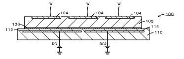
- a transfer Al 2 O 3 plate 102 including a plurality of wafer mounting portions 104 on which a wafer W is mounted is disposed on the upper surface of an AlN electrostatic chuck 110.
- a plating layer 106 of a conductive material (for example, Ni) is formed on the back surface of the transport Al 2 O 3 plate 102.
- the AlN electrostatic chuck 110 includes a pair of positive and negative electrodes 112 and 114.
- the plating layer 106 of the transfer Al 2 O 3 plate 102 and the AlN electrostatic chuck 110 are applied.
- a Johnson-Rahbek force JR force
- JR force is generated between the Al 2 O 3 plate 102 and the AlN electrostatic chuck 110.
- the surface of the wafer mounting portion 104 (the surface in contact with the wafer W) is a ground surface.
- an emboss (not shown) is formed on the surface of the AlN electrostatic chuck 110 that faces the plating layer 106, and the surface of the emboss (the surface that contacts the plating layer 106) is a mirror surface.
- the wafer W is only placed on the wafer placement portion 104 of the transfer Al 2 O 3 plate 102, so that the wafer W and the surface of the wafer placement portion 104 are not affected.
- High contact thermal resistance Therefore, when there is plasma heat input from the top, the temperature of the wafer W may become too high, or the temperature distribution of the wafer W (difference between the highest temperature and the lowest temperature) may become too large.
- the present invention has been made in view of the above-mentioned problems, and has as its main object to prevent the wafer from becoming too hot or the temperature distribution of the wafer from becoming too large.
- the wafer support structure of the present invention comprises: A ceramic tray plate having a plurality of wafer mounting portions for mounting a wafer is a wafer support structure arranged on the upper surface of a ceramic base plate,
- the base plate incorporates a base side electrode
- the tray plate contains a tray side electrode, By adjusting the voltage applied to the base side electrode and the tray side electrode in a state where the wafer is placed on the wafer placement unit, an electrostatic force that pulls the base plate and the tray plate together is generated. And generating an electrostatic force that pulls the tray plate and the wafer together, Is.
- the tray plate has a metal layer on a surface facing the base plate, and the base side electrode and the tray side electrode in a state where the wafer is placed on the wafer placement unit.
- the tray plate does not have a metal layer on the surface opposed to the base plate, and a voltage is applied to the tray side electrode in a state where the wafer is placed on the wafer placement portion, thereby the base plate and An electrostatic force that pulls the tray plate toward each other may be generated, and an electrostatic force that pulls the tray plate and the wafer toward each other may be generated.
- the surface of the wafer mounting portion that contacts the wafer may be a flat mirror surface.
- the tray plate may be made of Al 2 O 3 and the base plate may be made of AlN.
- the tray side electrode has a bipolar structure having a negative electrode and a positive electrode, and an area ratio of the negative electrode to the positive electrode in each wafer mounting portion is 0.7 to 1: 0. It may be 7 to 1 (preferably 0.9 to 1: 0.9 to 1). By doing this, it becomes difficult for the wafer to have a strong and weak adsorption force, and the temperature distribution of the wafer can be made smaller.
- FIG. 1 is a longitudinal sectional view of a wafer support structure 10 according to a first embodiment.
- the longitudinal cross-sectional view of the wafer support structure 40 of 3rd Embodiment. 1 is a longitudinal sectional view of a conventional wafer support structure 100.
- FIG. 1 is a longitudinal sectional view of a conventional wafer support structure 100.
- FIG. 1 is a longitudinal sectional view of a wafer support structure 10 according to the first embodiment
- FIG. 2 is a plan view of the wafer support structure 10.
- the wafer support structure 10 is used to support a wafer W for performing CVD, etching, and the like using plasma, and is attached inside a semiconductor process chamber (not shown).
- the wafer support structure 10 includes a ceramic (here, Al 2 O 3 ) tray plate 12 having a plurality of wafer placement portions 14 on which a wafer W is placed, and a ceramic (here, AlN) base plate 20. It is arranged on the upper surface.
- a ceramic (here, Al 2 O 3 ) tray plate 12 having a plurality of wafer placement portions 14 on which a wafer W is placed, and a ceramic (here, AlN) base plate 20. It is arranged on the upper surface.
- the tray plate 12 is a disk-shaped plate for carrying the wafer W, and has a plurality of wafer mounting portions 14 on the upper surface.
- the wafer mounting portion 14 is a hollow having a circular shape when viewed from above, and is formed to be slightly larger than the disk-shaped wafer W.
- a total of seven wafer mounting portions 14 are formed, one at the center when the tray plate 12 is viewed from above, and six at 60 ° on a concentric circle of the tray plate 12 (see FIG. 2).
- the surface of the wafer mounting portion 14, that is, the surface in contact with the wafer W is finished to be a flat mirror surface.
- the tray plate 12 incorporates a disk-shaped tray side electrode 18.
- the tray side electrode 18 is embedded at a position of 0.35 ⁇ 0.05 mm from the surface of the wafer mounting portion 14.
- the power supply pins 17 of the tray side electrode 18 reach the tray side electrode 18 through the base plate 20 from the lower surface of the base plate 20.
- the tip of the power supply pin 17 may be a flat surface or a curved surface (spherical surface).
- the base plate 20 is a disk-shaped plate and includes a base side electrode 22.
- the base-side electrode 22 is composed of a comb-teeth negative electrode 22a and a comb-teeth positive electrode 22b, and is arranged so that the mutual comb teeth enter alternately while maintaining a non-contact state.
- the area ratio of the comb-shaped negative electrode 22a and the comb-shaped positive electrode 22b is 0.7 to 1: 0.7 to 1.
- the base side electrode 22 is embedded at a position of 1 ⁇ 0.5 mm from the upper surface.
- a plurality of embosses are formed on the upper surface of the base plate 20, that is, the surface facing the tray plate 12. These embossed surfaces (surfaces in contact with the plating layer 16) are mirror-finished.
- the base plate 20 includes power supply pins 24a that reach the comb-shaped negative electrode 22a from the lower surface and power supply pins 24b that reach the comb-shaped positive electrode 22b from the lower surface.
- an insulating sleeve 26 is provided in the base plate 20 so as to penetrate in the vertical direction.
- the power supply pin 17 of the tray side electrode 18 is inserted through the insulating sleeve 26.
- the power supply pin 17 is adjusted by an elastic body (not shown) provided in the insulating sleeve 26 so that the contact load to the tray side electrode 18 is 200 g.
- the tray side electrode 18 and the base side electrode 22 may be formed by printing or may be formed by embedding a mesh.
- the wafer W is placed on each wafer placement unit 14. Then, the voltages of the DC power supplies DC1 and DC2 are applied to the power supply pins 24a and 24b, respectively, and the voltage of the DC power supply DC3 is applied to the power supply pin 17. Further, a high frequency voltage is applied to a parallel plate (not shown) to generate plasma above the wafer W. The plasma serves as a ground electrode for the wafer W. As a result, a JR force is generated between the base side electrode 22 and the plating layer 16 of the tray plate 12, and a Coulomb force is generated between the tray side electrode 18 and each wafer W. In this state, the wafer W is subjected to CVD film formation or etching using plasma.
- the contact thermal resistance between the wafer W and the wafer mounting unit 14 is such that no attracting force is generated between the wafer W and the wafer mounting unit 14. Smaller than For this reason, when the wafer W is heated from above, it is possible to prevent the wafer W from becoming too hot or the temperature distribution of the wafer W from becoming too large. Moreover, since the surface which contacts the wafer W among the wafer mounting parts 14 is a flat mirror surface, compared with the case where this surface is a grinding surface, the contact area of the wafer W and the wafer mounting part 14 becomes large, The effect of the present invention is remarkably obtained.
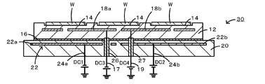
- the wafer support structure 30 of the second embodiment is the same as the wafer support structure 10 except that the configuration of the tray side electrode of the tray plate 12 is changed as shown in FIG. Specifically, the wafer support structure 30 is configured such that the tray-side electrode built in the tray plate 12 is composed of a zigzag negative electrode 18a and a positive electrode 18b, and these are alternately inserted while maintaining a non-contact state with each other. did. Further, the power supply pin 17 was connected to the negative electrode 18a, and the power supply pin 19 was connected to the positive electrode 18b. The power supply pin 19 is inserted through an insulating sleeve 27 that penetrates the base plate 20.
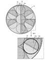
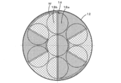
- FIGS. 4 and 5 and 6 show examples in which 7 4-inch wafers W are placed on the tray plate 12.
- the negative electrode 18a is shown with a fine mesh
- the positive electrode 18b is shown with a coarse mesh.
- the distance between the negative electrode 18a and the positive electrode 18b is not particularly limited, but may be 2 to 6 mm, for example.
- the distance between the electrode end (outer peripheral end) of the tray side electrode 18 and the tray plate 12 is not particularly limited, but is preferably 1 to 4 mm, for example. 4 to 6, when one wafer W is viewed, the area ratio of the negative electrode 18 a and the positive electrode 18 b is 0.7 to 1: 0.7 to 1 (1 to 1 in FIGS. 4 to 6).
- the wafer support structure 30 first, the wafer W is placed on each wafer placement unit 14. Then, the voltages of the DC power supplies DC1 and DC2 are applied to the power supply pins 24a and 24b, respectively, and the voltages of the DC power supplies DC3 and DC4 are applied to the power supply pins 17 and 19, respectively.
- a high frequency voltage is applied to a parallel plate (not shown) to generate plasma above the wafer W.
- a JR force is generated between the base-side electrode 22 and the plating layer 16 of the tray plate 12, and a Coulomb force is generated between the tray-side electrode (the negative electrode 18a and the positive electrode 18b) and each wafer W. Therefore, the same effect as the wafer support structure 10 can be obtained.
- the area ratio of the negative electrode 18a and the positive electrode 18b is 0.7 to 1: 0.7 to 1 when one wafer W is viewed, each wafer W is less likely to have a strong and weak adsorption force. Thus, the temperature distribution of the wafer W can be reduced.
- the wafer support structure 40 of the third embodiment supports the wafer except that the plating layer 16 of the tray plate 12 is not formed and the configuration of the base side electrode of the base plate 20 is changed.
- This is the same as the structure 10.
- the wafer support structure 40 was placed directly on the base plate 20 without forming the plating layer 16 on the lower surface of the tray plate 12.
- the base-side electrode 42 of the base plate 20 was a single disk-like electrode, and this was grounded by the earth pin 42a.
- the base side electrode 42 was disposed at 0.5 ⁇ 3 mm from the upper surface.
- the tray side electrode 18 was arranged at 0.35 ⁇ 0.05 mm from the surface of the wafer mounting surface 14 and the lower surface of the tray plate 12.
- the wafer W is mounted on each wafer mounting unit 14. Then, the voltage of the DC power supply DC1 is applied to each of the power supply pins 17. Further, a high frequency voltage is applied to a parallel plate (not shown) to generate plasma above the wafer W. The plasma serves as a ground electrode for the wafer W. Thereby, a Coulomb force is generated between the base-side electrode 42 and the tray-side electrode 18, and a Coulomb force is generated between the tray-side electrode 18 and each wafer W. Therefore, the same effect as the wafer support structure 10 can be obtained.
- the volume resistivity of the tray plate 12 at the use temperature is preferably 1 ⁇ 10 15 ⁇ cm or more.
- the temperature and temperature distribution of the wafer W when plasma heat input was generated were measured.
- ⁇ 500 V, +500 V, and ⁇ 2.5 kV were applied to DC power supplies DC1, DC2, and DC3, respectively.
- ⁇ 500 V, +500 V, ⁇ 2.5 kV, and +2.5 kV were applied to DC power supplies DC1, DC2, DC3, and DC4, respectively.
- Wafer support structure 40 applied ⁇ 2.5 kV to DC power supply DC1.
- ⁇ 500V and + 500V were applied to DC power supplies DC1 and DC2, respectively. With the voltage applied in this manner, the plasma heat input was set to 1 kW for each wafer support structure 10, 30, 40, 100, and the temperature of the base plate 20 was controlled to 40 ° C.
- the present invention can be used in a wafer processing apparatus that performs film formation, etching, and the like on a wafer.
Landscapes
- Container, Conveyance, Adherence, Positioning, Of Wafer (AREA)
Abstract
Description
ウエハを載置するウエハ載置部を複数備えたセラミック製のトレイプレートがセラミック製のベースプレートの上面に配置されたウエハ支持構造体であって、
前記ベースプレートは、ベース側電極を内蔵し、
前記トレイプレートは、トレイ側電極を内蔵し、
前記ウエハ載置部に前記ウエハを載置した状態で前記ベース側電極及び前記トレイ側電極に印加する電圧を調整することにより、前記ベースプレートと前記トレイプレートとを互いに引き寄せる静電気的な力を発生させると共に前記トレイプレートと前記ウエハとを互いに引き寄せる静電気的な力を発生させる、
ものである。
本発明のウエハ支持構造体の一例を図1及び図2を用いて以下に説明する。図1は、第1実施形態のウエハ支持構造体10の縦断面図、図2は、ウエハ支持構造体10の平面図である。
第2実施形態のウエハ支持構造体30は、図3に示すように、トレイプレート12のトレイ側電極の構成を変更したこと以外は、ウエハ支持構造体10と同様である。具体的には、ウエハ支持構造体30は、トレイプレート12に内蔵したトレイ側電極をジグザグ形状の負極18aと正極18bとで構成し、これらを互いに非接触状態を保ちつつ交互に入り込むように配置した。また、負極18aに給電ピン17を接続し、正極18bに給電ピン19を接続した。給電ピン19はベースプレート20を貫通する絶縁スリーブ27を挿通するようにした。更に、給電ピン17,19には、それぞれ直流電源DC3,DC4の電圧を印加するようにした。ここで、トレイプレート12を上方から見たときの透視図を図4~図6に示す。図4は2インチのウエハWをトレイプレート12に21個載置した例、図5及び図6は4インチのウエハWをトレイプレート12に7個載置した例である。各図において、負極18aを細かいメッシュ、正極18bを粗いメッシュで示した。負極18aと正極18bとの間隔は、特に限定するものではないが、例えば2~6mmにすればよい。また、トレイ側電極18の電極端(外周端)とトレイプレート12との距離も、特に限定するものではないが、例えば1~4mmとするのが好ましい。図4~図6のいずれも、1つのウエハWをみたときに負極18aと正極18bの面積比が0.7~1:0.7~1(図4~図6では1:1)となるように設定した。このウエハ支持構造体30を使用するにあたっては、まず、各ウエハ載置部14にウエハWを載置する。そして、給電ピン24a,24bにそれぞれ直流電源DC1,DC2の電圧を印加し、給電ピン17,19に直流電源DC3,DC4の電圧を印加する。また、図示しない平行平板に高周波電圧を印加してウエハWの上方にプラズマを発生させる。これにより、ベース側電極22とトレイプレート12のめっき層16との間でJR力が発生し、トレイ側電極(負極18aと正極18b)と各ウエハWとの間でクーロン力が発生する。したがって、ウエハ支持構造体10と同様の効果が得られる。また、1つのウエハWをみたときに負極18aと正極18bの面積比が0.7~1:0.7~1となるようにしたため、各ウエハWは吸着力の強いところと弱いところが生じにくくなり、ウエハWの温度分布を小さくすることができる。
第3実施形態のウエハ支持構造体40は、図7に示すように、トレイプレート12のめっき層16を形成しなかったこと、ベースプレート20のベース側電極の構成を変更したこと以外は、ウエハ支持構造体10と同様である。具体的には、ウエハ支持構造体40は、トレイプレート12の下面にめっき層16を形成せず直接ベースプレート20に載置した。また、ベースプレート20のベース側電極42は1枚の円盤状の電極とし、これをアースピン42aで接地した。ベース側電極42は、上面から0.5±3mmに配置した。また、トレイ側電極18は、ウエハ載置面14の表面及びトレイプレート12の下面から0.35±0.05mmに配置した。このウエハ支持構造体40を使用するにあたっては、まず、各ウエハ載置部14にウエハWを載置する。そして、給電ピン17にそれぞれ直流電源DC1の電圧を印加する。また、図示しない平行平板に高周波電圧を印加してウエハWの上方にプラズマを発生させる。プラズマは、ウエハWのグランド電極の役割を果たす。これにより、ベース側電極42とトレイ側電極18との間でクーロン力が発生し、トレイ側電極18と各ウエハWとの間でクーロン力が発生する。したがって、ウエハ支持構造体10と同様の効果が得られる。なお、トレイプレート12の使用温度における体積抵抗率は、1×1015Ωcm以上とするのが好ましい。

Claims (5)
- ウエハを載置するウエハ載置部を複数備えたセラミック製のトレイプレートがセラミック製のベースプレートの上面に配置されたウエハ支持構造体であって、
前記ベースプレートは、ベース側電極を内蔵し、
前記トレイプレートは、トレイ側電極を内蔵し、
前記ウエハ載置部に前記ウエハを載置した状態で前記ベース側電極及び前記トレイ側電極に印加する電圧を調整することにより、前記ベースプレートと前記トレイプレートとを互いに引き寄せる静電気的な力を発生させると共に前記トレイプレートと前記ウエハとを互いに引き寄せる静電気的な力を発生させる、
ウエハ支持構造体。 - 前記トレイプレートは、前記ベースプレートと対向する面に金属層を有し、
前記ウエハ載置部に前記ウエハを載置した状態で前記ベース側電極及び前記トレイ側電極の両方に電圧を印加することにより、前記ベースプレートと前記トレイプレートの前記金属層とを互いに引き寄せる静電気的な力を発生させると共に、前記トレイプレートと前記ウエハとを互いに引き寄せる静電気的な力を発生させる、
請求項1に記載のウエハ支持構造体。 - 前記トレイプレートは、前記ベースプレートと対向する面に金属層を有さず、
前記ウエハ載置部に前記ウエハを載置した状態で前記トレイ側電極に電圧を印加することにより、前記ベースプレートと前記トレイプレートとを互いに引き寄せる静電気的な力を発生させると共に、前記トレイプレートと前記ウエハとを互いに引き寄せる静電気的な力を発生させる、
請求項1に記載のウエハ支持構造体。 - 前記トレイプレートは、Al2O3製であり、
前記ベースプレートは、AlN製である、
請求項1~3のいずれか1項に記載のウエハ支持構造体。 - 前記トレイ側電極は、負極と正極とを有する双極構造であり、各ウエハ載置部における前記負極と前記正極との面積比は0.7~1:0.7~1である、
請求項1~4のいずれか1項に記載のウエハ支持構造体。
Priority Applications (4)
| Application Number | Priority Date | Filing Date | Title |
|---|---|---|---|
| JP2016520171A JP6010720B1 (ja) | 2015-01-20 | 2016-01-13 | ウエハ支持構造体 |
| KR1020167030451A KR101910727B1 (ko) | 2015-01-20 | 2016-01-13 | 웨이퍼 지지 구조체 |
| CN201680001162.4A CN106233450B (zh) | 2015-01-20 | 2016-01-13 | 晶片支承构造体 |
| US15/335,839 US10332774B2 (en) | 2015-01-20 | 2016-10-27 | Wafer support structure |
Applications Claiming Priority (2)
| Application Number | Priority Date | Filing Date | Title |
|---|---|---|---|
| US201562105371P | 2015-01-20 | 2015-01-20 | |
| US62/105371 | 2015-01-20 |
Related Child Applications (1)
| Application Number | Title | Priority Date | Filing Date |
|---|---|---|---|
| US15/335,839 Continuation US10332774B2 (en) | 2015-01-20 | 2016-10-27 | Wafer support structure |
Publications (1)
| Publication Number | Publication Date |
|---|---|
| WO2016117427A1 true WO2016117427A1 (ja) | 2016-07-28 |
Family
ID=56416974
Family Applications (1)
| Application Number | Title | Priority Date | Filing Date |
|---|---|---|---|
| PCT/JP2016/050817 Ceased WO2016117427A1 (ja) | 2015-01-20 | 2016-01-13 | ウエハ支持構造体 |
Country Status (6)
| Country | Link |
|---|---|
| US (1) | US10332774B2 (ja) |
| JP (1) | JP6010720B1 (ja) |
| KR (1) | KR101910727B1 (ja) |
| CN (1) | CN106233450B (ja) |
| TW (1) | TWI584407B (ja) |
| WO (1) | WO2016117427A1 (ja) |
Cited By (1)
| Publication number | Priority date | Publication date | Assignee | Title |
|---|---|---|---|---|
| JP2018010975A (ja) * | 2016-07-14 | 2018-01-18 | サムコ株式会社 | プラズマ処理装置用のトレイ |
Families Citing this family (4)
| Publication number | Priority date | Publication date | Assignee | Title |
|---|---|---|---|---|
| JP6714562B2 (ja) * | 2017-09-20 | 2020-06-24 | 株式会社Kokusai Electric | 基板処理装置、半導体装置の製造方法およびプログラム |
| KR102677251B1 (ko) * | 2021-10-28 | 2024-06-20 | 세메스 주식회사 | 기판 테스트 장치 및 이를 이용하는 디척킹 포스 측정 방법 |
| CN114141683A (zh) * | 2021-11-26 | 2022-03-04 | 北京北方华创微电子装备有限公司 | 静电托盘及基座 |
| CN114695243B (zh) * | 2022-03-02 | 2024-10-25 | 北京北方华创微电子装备有限公司 | 半导体腔室的承载装置及半导体腔室 |
Citations (3)
| Publication number | Priority date | Publication date | Assignee | Title |
|---|---|---|---|---|
| JP2004095665A (ja) * | 2002-08-29 | 2004-03-25 | Tokyo Electron Ltd | 静電吸着装置および処理装置 |
| WO2011151996A1 (ja) * | 2010-06-01 | 2011-12-08 | パナソニック株式会社 | プラズマ処理装置及びプラズマ処理方法 |
| JP2014534620A (ja) * | 2011-10-06 | 2014-12-18 | エーエスエムエル ネザーランズ ビー.ブイ. | チャック、リソグラフィ装置及びチャックを使用する方法 |
Family Cites Families (13)
| Publication number | Priority date | Publication date | Assignee | Title |
|---|---|---|---|---|
| JP4256503B2 (ja) | 1997-10-30 | 2009-04-22 | 東京エレクトロン株式会社 | 真空処理装置 |
| KR100404778B1 (ko) | 1998-10-29 | 2003-11-07 | 동경 엘렉트론 주식회사 | 진공 처리 장치 |
| JP2003124298A (ja) * | 2001-10-17 | 2003-04-25 | Anelva Corp | プラズマ支援ウェハー処理反応容器の二重静電チャックウェハーステージ |
| JP4482472B2 (ja) * | 2005-03-24 | 2010-06-16 | 日本碍子株式会社 | 静電チャック及びその製造方法 |
| KR100663749B1 (ko) | 2005-04-28 | 2007-01-03 | 에피밸리 주식회사 | 발광소자 기판용 서셉터 |
| US8961691B2 (en) | 2008-09-04 | 2015-02-24 | Tokyo Electron Limited | Film deposition apparatus, film deposition method, computer readable storage medium for storing a program causing the apparatus to perform the method |
| JP5173684B2 (ja) | 2008-09-04 | 2013-04-03 | 東京エレクトロン株式会社 | 成膜装置、成膜方法、並びにこの成膜方法を成膜装置に実施させるプログラム及びこれを記憶するコンピュータ可読記憶媒体 |
| KR101331372B1 (ko) * | 2009-02-18 | 2013-11-20 | 가부시키가이샤 알박 | 웨이퍼 반송용 트레이 및 이 트레이 상에 웨이퍼를 고정시키는 방법 |
| WO2010109848A1 (ja) * | 2009-03-26 | 2010-09-30 | パナソニック株式会社 | プラズマ処理装置及びプラズマ処理方法 |
| JP2011114178A (ja) * | 2009-11-27 | 2011-06-09 | Samco Inc | プラズマ処理装置及びプラズマ処理方法 |
| WO2013049586A1 (en) * | 2011-09-30 | 2013-04-04 | Applied Materials, Inc. | Electrostatic chuck |
| US10825708B2 (en) * | 2011-12-15 | 2020-11-03 | Applied Materials, Inc. | Process kit components for use with an extended and independent RF powered cathode substrate for extreme edge tunability |
| JP6377975B2 (ja) * | 2014-06-23 | 2018-08-22 | 新光電気工業株式会社 | 基板固定装置 |
-
2016
- 2016-01-13 KR KR1020167030451A patent/KR101910727B1/ko active Active
- 2016-01-13 JP JP2016520171A patent/JP6010720B1/ja active Active
- 2016-01-13 CN CN201680001162.4A patent/CN106233450B/zh active Active
- 2016-01-13 WO PCT/JP2016/050817 patent/WO2016117427A1/ja not_active Ceased
- 2016-01-18 TW TW105101347A patent/TWI584407B/zh active
- 2016-10-27 US US15/335,839 patent/US10332774B2/en active Active
Patent Citations (3)
| Publication number | Priority date | Publication date | Assignee | Title |
|---|---|---|---|---|
| JP2004095665A (ja) * | 2002-08-29 | 2004-03-25 | Tokyo Electron Ltd | 静電吸着装置および処理装置 |
| WO2011151996A1 (ja) * | 2010-06-01 | 2011-12-08 | パナソニック株式会社 | プラズマ処理装置及びプラズマ処理方法 |
| JP2014534620A (ja) * | 2011-10-06 | 2014-12-18 | エーエスエムエル ネザーランズ ビー.ブイ. | チャック、リソグラフィ装置及びチャックを使用する方法 |
Cited By (1)
| Publication number | Priority date | Publication date | Assignee | Title |
|---|---|---|---|---|
| JP2018010975A (ja) * | 2016-07-14 | 2018-01-18 | サムコ株式会社 | プラズマ処理装置用のトレイ |
Also Published As
| Publication number | Publication date |
|---|---|
| JPWO2016117427A1 (ja) | 2017-04-27 |
| US10332774B2 (en) | 2019-06-25 |
| TW201639071A (zh) | 2016-11-01 |
| CN106233450B (zh) | 2018-12-28 |
| CN106233450A (zh) | 2016-12-14 |
| US20170047239A1 (en) | 2017-02-16 |
| KR20160138285A (ko) | 2016-12-02 |
| TWI584407B (zh) | 2017-05-21 |
| JP6010720B1 (ja) | 2016-10-19 |
| KR101910727B1 (ko) | 2018-10-22 |
Similar Documents
| Publication | Publication Date | Title |
|---|---|---|
| JP6010720B1 (ja) | ウエハ支持構造体 | |
| JP6441927B2 (ja) | 局部的に加熱されるマルチゾーン式の基板支持体 | |
| US10373853B2 (en) | Electrostatic chuck and wafer processing apparatus | |
| TWI644393B (zh) | Electrostatic chuck | |
| US9837297B2 (en) | Tray and wafer holding apparatus | |
| TW527264B (en) | Ceramic electrostatic chuck assembly and method of making | |
| JP6251461B1 (ja) | 静電チャックヒータ | |
| CN104472010B (zh) | 陶瓷加热器加热丝的结构 | |
| TW201344841A (zh) | 具有減低能量損失的靜電夾盤 | |
| US20090041980A1 (en) | Electrostatic Chuck and Electrode Sheet for Electrostatic Chuck | |
| CN116264180B (zh) | 晶片载放台 | |
| JP2017212332A (ja) | 電極内蔵型載置台構造 | |
| US10679873B2 (en) | Ceramic heater | |
| JP4339306B2 (ja) | 吸着方法 | |
| TWI844329B (zh) | 靜電吸盤 | |
| JP2017034042A (ja) | ウエハ支持装置 | |
| JP2005116686A (ja) | 双極型静電チャック | |
| JP6704791B2 (ja) | 加熱装置 | |
| TW202601913A (zh) | 陶瓷基座 | |
| JP6695204B2 (ja) | 保持装置 | |
| TWI533397B (zh) | A placing table of the plasma processing apparatus, and a corresponding plasma processing apparatus | |
| JP2006054445A (ja) | 吸着装置 |
Legal Events
| Date | Code | Title | Description |
|---|---|---|---|
| ENP | Entry into the national phase |
Ref document number: 2016520171 Country of ref document: JP Kind code of ref document: A |
|
| 121 | Ep: the epo has been informed by wipo that ep was designated in this application |
Ref document number: 16740034 Country of ref document: EP Kind code of ref document: A1 |
|
| ENP | Entry into the national phase |
Ref document number: 20167030451 Country of ref document: KR Kind code of ref document: A |
|
| NENP | Non-entry into the national phase |
Ref country code: DE |
|
| 122 | Ep: pct application non-entry in european phase |
Ref document number: 16740034 Country of ref document: EP Kind code of ref document: A1 |