WO2016114170A1 - プローブカードおよびこのプローブカードが備える積層配線基板 - Google Patents
プローブカードおよびこのプローブカードが備える積層配線基板 Download PDFInfo
- Publication number
- WO2016114170A1 WO2016114170A1 PCT/JP2016/050100 JP2016050100W WO2016114170A1 WO 2016114170 A1 WO2016114170 A1 WO 2016114170A1 JP 2016050100 W JP2016050100 W JP 2016050100W WO 2016114170 A1 WO2016114170 A1 WO 2016114170A1
- Authority
- WO
- WIPO (PCT)
- Prior art keywords
- electrode
- wiring
- plane
- resin
- plane electrode
- Prior art date
- Legal status (The legal status is an assumption and is not a legal conclusion. Google has not performed a legal analysis and makes no representation as to the accuracy of the status listed.)
- Ceased
Links
Images




Classifications
-
- G—PHYSICS
- G01—MEASURING; TESTING
- G01R—MEASURING ELECTRIC VARIABLES; MEASURING MAGNETIC VARIABLES
- G01R1/00—Details of instruments or arrangements of the types included in groups G01R5/00 - G01R13/00 and G01R31/00
- G01R1/02—General constructional details
- G01R1/06—Measuring leads; Measuring probes
- G01R1/067—Measuring probes
- G01R1/073—Multiple probes
-
- H—ELECTRICITY
- H05—ELECTRIC TECHNIQUES NOT OTHERWISE PROVIDED FOR
- H05K—PRINTED CIRCUITS; CASINGS OR CONSTRUCTIONAL DETAILS OF ELECTRIC APPARATUS; MANUFACTURE OF ASSEMBLAGES OF ELECTRICAL COMPONENTS
- H05K3/00—Apparatus or processes for manufacturing printed circuits
- H05K3/46—Manufacturing multilayer circuits
Definitions
- the present invention relates to a probe card used for electrical inspection of an object to be inspected and a laminated wiring board provided in the probe card.
- a ceramic multilayer substrate is widely used as a substrate for forming a connection wiring between an external electrode of a mother substrate and a probe pin.
- the number of terminals and the pitch of terminals have been reduced, so that some layers of a ceramic multilayer substrate can be easily formed with polyimide or the like.
- a laminated wiring board replaced with a resin layer is used.
- a plurality of surface electrodes 103 connected to the probe pins are formed on the upper surface of the multilayer wiring substrate 100 at a narrow pitch.
- a plurality of back surface electrodes 104 are formed on the lower surface of the multilayer wiring substrate 100 so as to correspond to the front surface electrodes 103 and are respectively connected to the corresponding front surface electrodes 103.
- Each back electrode 104 is provided for connection with a mother substrate.
- a rewiring structure is formed inside the resin laminate 102 and the ceramic laminate 101 so that the pitch between the adjacent back surface electrodes 104 is wider than the pitch between the adjacent front surface electrodes 103.
- the resin laminate 102 closer to the surface electrode 103 it is necessary to make the wiring formed in the inside thin and to reduce the distance between adjacent wirings. It is composed of a resin layer 102a made of polyimide or the like that can form an appropriate wiring.
- the ceramic laminate 101 that has a relatively large space for wiring formation is composed of the ceramic layer 101a having higher rigidity than the resin layer 102a and having a linear expansion coefficient close to that of an inspection medium such as an IC wafer. Yes.
- the wiring pattern formed on the resin laminate 102 is fine, while the wiring resistance is high. Therefore, conventionally, in order to reduce the wiring resistance of a wiring pattern through which a large current flows, a plate-like electrode (so-called solid electrode) having a large area may be provided in a part of the wiring pattern.
- an electrode having a large area such as a solid electrode, is disposed directly below the surface electrode 103 connected to the probe pin, and both are connected to the via. If the connection is made via an interlayer connection conductor such as a conductor, the stress when the probe pin is pressed against the surface electrode 103 may act directly on the solid electrode, and the solid electrode may peel from the resin layer 102a.
- the present invention has been made in view of the above-described problems, and in a laminated wiring board for a probe card having a laminate of resin layers, a flat electrode having a large area (so-called solid electrode) provided to reduce wiring resistance. ) Is prevented from peeling from the resin layer.
- a laminated wiring board for a probe card includes a core substrate, a plurality of resin layers, and a plurality of wiring layers, and the resin layers and the wiring layers are alternately laminated.
- a resin laminate laminated on the core substrate, a probe pin connection pad electrode provided on the resin layer located on the outermost layer of the resin laminate, and an inner layer of the resin laminate A planar first in-plane electrode provided in a predetermined wiring layer, and a connection wiring for connecting the pad electrode and the first in-plane electrode, the pad electrode and the first in-plane electrode;
- a plurality of resin layers are arranged between the plurality of resin layers, and the connection wiring includes a plurality of through conductors for interlayer connection provided in each of the resin layers between the pad electrode and the first in-plane electrode.
- a plane in the line electrode provided on the layer, at least one of the plurality of through conductors is characterized in that it is arranged offset so as not to overlap with the pad electrode in plan view.
- connection wiring since at least one of the plurality of through conductors included in the connection wiring is arranged so as not to overlap the pad electrode in plan view, the first from the probe pin when inspecting the inspection object.
- the stress acting on the in-plane electrode can be reduced, and thereby the peeling of the first in-plane electrode from the resin layer can be reduced.
- connection wiring may include a branch wiring that branches in the middle of a path from the pad electrode to the first in-plane electrode, and the branch wiring may be connected to the first in-plane electrode. If it does in this way, since the wiring resistance as the whole connection wiring which connects a pad electrode and the 1st in-plane electrode can be lowered
- a flat plate-like second in-plane electrode may be provided on the wiring layer disposed between the pad electrode and the first in-plane electrode.
- the first in-plane electrode may be arranged so as to be shifted so as not to overlap the pad electrode in plan view.
- the region directly under the pad electrode is greatly affected by stress from the probe pin and heat generated when the probe card is used. Therefore, by shifting the first in-plane electrode from the pad electrode, it is possible to suppress these influences, and therefore it is possible to reduce peeling of the first in-plane electrode from the resin layer.
- the first in-plane electrode may be provided with a first through hole at a position overlapping the pad electrode in plan view.
- the first through hole As described above, by forming the electrode non-formation region by the first through hole directly under the pad electrode, the stress acting on the first in-plane electrode when the probe pin is pressed against the object to be inspected is relieved. Therefore, peeling of the first in-plane electrode from the resin layer can be reduced.
- the resin of the resin layer located in the upper and lower sides of the first in-plane electrode enters the first through hole, and the two are in close contact with each other. Since the adhesion strength between the resin layers is stronger than the adhesion strength between the first in-plane electrode and the resin layer, providing the first through hole can reinforce the adhesion between the first in-plane electrode and the resin layer. it can.
- first in-plane electrode may further be provided with a second through hole at a position different from the first through hole.
- the close contact between the first in-plane electrode and the resin layer is further reinforced by the second through-hole, peeling of the first in-plane electrode from the resin layer can be further reduced.
- the above-described multilayer wiring board for probe cards may be used for a probe card for performing an electrical inspection of an object to be inspected.
- the connection wiring since the pad electrode and the flat first in-plane electrode are connected by the connection wiring, the wiring resistance of the wiring line including the connection wiring and the first in-plane electrode can be reduced.
- the first in-plane electrode since at least one of the plurality of through conductors included in the connection wiring is arranged so as not to overlap the pad electrode in a plan view, the first in-plane electrode is removed from the probe pin when inspecting the inspection object. The stress acting on the first in-plane electrode can be reduced from the resin layer.
- FIGS. 1 is a cross-sectional view of the probe card 1
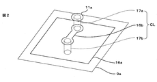
- FIG. 2 is a diagram for explaining the connection wiring CL of FIG. 1
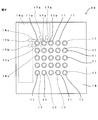
- FIG. 3 is a plan view of the multilayer wiring board 3a of FIG.
- a probe card 1 As shown in FIG. 1, a probe card 1 according to this embodiment includes a mother board 2, a multilayer wiring board 3a mounted on one main surface of the mother board 2, and a plurality of wiring boards connected to the multilayer wiring board 3a.
- the probe head 4 that supports the probe pins 5, 5 a, and 5 b and the cover body 21 that fixes the probe head 4 are used, for example, for electrical inspection of an inspection object 50 such as a semiconductor element.
- the mother substrate 2 has a plurality of mounting electrodes 6 for mounting the multilayer wiring board 3a on one main surface, and a plurality of external electrodes 7 for external connection formed on the other main surface.
- each mounting electrode 6 is connected to a predetermined external electrode 7 by a wiring electrode 30 or a via conductor 31 formed inside the mother substrate.
- the mother substrate 2 is made of, for example, glass epoxy resin.
- the probe head 4 that holds the probe pins 5, 5 a, 5 b is fixed to a cover body 21 that is fixed to the mother board 2.
- the laminated wiring board 3 a includes a core substrate 8 disposed on the mother substrate 2 side, and a resin laminate 9 laminated on the core substrate 8.
- the core substrate 8 includes a plurality (three layers in this embodiment) of ceramic layers 8a and a plurality of wiring layers 8b.
- the ceramic layers 8a and the wiring layers 8b are alternately stacked.
- Each ceramic layer 8a may be formed of various ceramics such as a low-temperature co-fired ceramic (LTCC) mainly composed of a ceramic (for example, alumina) containing borosilicate glass and a high-temperature fired ceramic (HTCC). it can.
- LTCC low-temperature co-fired ceramic
- HTCC high-temperature fired ceramic
- the resin laminate 9 has a plurality of resin layers 9a and a plurality of wiring layers 9b.
- the resin layers 9a and the wiring layers 9b are alternately laminated.
- Each resin layer 9a is formed of a resin such as polyimide, for example.
- Each ceramic layer 8a is formed with a plurality of via conductors 15 that connect the wiring electrodes 14 formed in different wiring layers 8b.
- Each via conductor 15 and each wiring electrode 14 are each formed of a metal such as Cu, Ag, or Al.
- the wiring electrode 14 formed on the wiring layer 8b can be formed by, for example, screen printing using a conductive paste containing the metal (Cu, Ag, Al, etc.).
- a plurality of external connection electrodes 10 for mounting on the mother substrate 2 are formed on the main surface of the core substrate 8 opposite to the resin laminate 9, and each of these external connection electrodes 10 is formed on the mother substrate 2. Each is connected to a predetermined mounting electrode 6 with solder.
- These external connection electrodes 10 are made of, for example, a metal such as Cu, Ag, or Al.
- Various wiring electrodes 16, 16 a and 16 b are formed on each wiring layer 9 b of the resin laminate 9.
- a plurality of pad electrodes 11, 11 a, 11 b connected to predetermined probe pins 5, 5 a, 5 b are formed on the resin layer 9 a located on the outermost layer of the resin laminate 9.
- wiring electrodes 16, 16a, 16b formed in different wiring layers 9b, each pad electrode 11, 11a, 11b and wiring electrodes 16, 16b in the resin laminate 9 are provided in each resin layer 9a.
- a plurality of via conductors 17, 17a, 17b to be connected are formed.
- an insulating coating film 18 for protecting the surface of the resin laminate 9 is laminated on the uppermost resin layer 9a.
- the insulating coating film 18 is laminated on the uppermost resin layer 9a with the pad electrodes 11, 11a, 11b exposed.
- the insulating coating film 18 is made of polyimide, like the resin layer 9a.
- each wiring electrode 16, 16a, 16b for example, a Ti film as a base electrode is formed on the main surface of a predetermined resin layer 9a by sputtering or the like, and a Cu film is similarly formed on the Ti film by sputtering or the like. . And it can form by forming a Cu film
- Each of the pad electrodes 11a to 11e is composed of, for example, a base electrode 12 formed of Cu or the like, and a surface electrode 13 formed by applying Ni / Au plating on the base electrode 12.
- each via conductor 17, 17a, 17b formed in the resin laminate 9 is formed simultaneously with each wiring electrode 16, 16a, 16b in the via hole after the via hole is formed. Is formed.
- each pad electrode 11, 11 a, 11 b is electrically connected to a predetermined external electrode 7 formed on the other main surface of the mother substrate 2.
- the pad electrodes 11, 11 a, 11 b are respectively connected to wiring electrodes 16, 16 a, 16 b and via conductors 17, 17 a, 17 b formed on the resin laminate 9, a core substrate.
- 8 is connected to a predetermined external electrode 7 via the wiring electrode 14 and the via conductor 15 formed in 8, and the wiring electrode 30 and the via conductor 31 formed in the mother substrate 2.
- each wiring electrode 14 formed on the core substrate 8 is formed by screen printing or the like, it becomes a thick film pattern.
- each wiring electrode 16, 16a, 16b formed on the resin laminate 9 is formed into a thin film pattern by sputtering or the like. Further, as the pad electrodes 11, 11a, 11b are narrowed, some of the wiring electrodes 16, 16b are thinned by photolithography. Therefore, the wiring electrodes 16 and 16 b formed thin and thin have higher wiring resistance than the wiring electrodes 14 formed on the core substrate 8.
- a flat plate-like first in-plane electrode 16a (so-called “so-called”) is provided in the wiring path in the resin laminate 9 connected to the power supply probe pins 5a and 5b through which a relatively large current flows.
- a solid electrode In the present embodiment, the first in-plane electrode 16a is a solid electrode for power supply wiring.
- the first in-plane electrode 16a is the lowermost wiring layer 9b (the wiring disposed between the second resin layer 9a and the third resin layer 9a from the top). Provided in layer 9b). Between these pad electrodes 11a and 11b and the first in-plane electrode 16a, two resin layers 9a and one wiring layer 9b are interposed, and a plurality of via conductors 17a provided in each of the resin layers 9a. , 17b and the wiring electrode 16b provided on the wiring layer 9b form two connection wirings CL for connecting the pad electrodes 11a, 11b and the first in-plane electrode 16a.
- the linear expansion coefficient is different between the wiring electrodes 16, 16a, 16b formed on the resin laminate 9 and the resin layer 9a, in particular, a solid electrode having a large area, such as the first in-plane electrode 16a. It is easy to peel off from the resin layer 9a due to heat generated when the probe card 1 is used. Further, since the probe pins 5a to 5e are frequently pressed against the object to be inspected when the probe card 1 is used, if the stress at this time acts on the first in-plane electrode 16a, the peeling from the resin layer 9a is promoted. There is a risk. Therefore, in this embodiment, the structure of the connection wiring CL is devised in order to reduce the peeling of the first in-plane electrode 16a from the resin layer 9a.
- the pad electrode 11a will be described as an example.
- the connection wiring CL is provided through the uppermost resin layer 9a, and the upper end surface is connected to the power supply pad electrode 11a.
- the wiring electrode 16b is formed on a wiring layer 9b sandwiched between resin layers 9a provided with both via conductors 17a and 17b.
- connection wiring CL connecting the other pad electrode 11b and the first in-plane electrode 16a has the same configuration. According to this configuration, the probe pins 5, 5 a, and 5 b are pressed against the inspection object 50 at the time of inspection, as compared with the configuration in which the pad electrode 11 a and the first in-plane electrode 16 a are linearly connected by the via conductor.
- each of the two via conductors 17a and 17b constituting the connection wiring CL corresponds to the “through conductor” of the present invention
- the wiring electrode 16b connecting both the via conductors 17a and 17b corresponds to the “in-plane line” of the present invention.
- the resin layer 9a interposed between the pad electrode 11a and the first in-plane electrode 16a may be two or more layers.
- the connection wiring CL is configured to have via conductors by the number of the resin layers 9a interposed therebetween.
- at least one of the via conductors is pad electrode 11a in plan view. It may be shifted so that it does not overlap.
- one via conductor 17b of the two via conductors 17a and 17b included in the connection wiring CL is disposed so as not to overlap the pad electrode 11a in plan view.
- the stress acting on the first in-plane electrode 16a from the probe pins 5, 5a, 5b can be reduced. Therefore, peeling of the first in-plane electrode 16a from the resin layer 9a can be reduced.
- the via conductor 17b which is a portion connected to the first in-plane electrode 16a of the connection wiring CL, is drawn out by the wiring electrode 16 and is disposed so as not to overlap the pad electrode 11a in plan view. The temperature rise at the connection portion between the first in-plane electrode 16a and the via conductor 17b can be reduced.
- FIGS. 4 is a cross-sectional view of the multilayer wiring board 3b
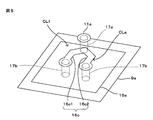
- FIG. 5 is a diagram for explaining the connection wiring CL1
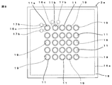
- FIG. 6 is a plan view of the multilayer wiring board 3b.
- the laminated wiring board 3b according to this embodiment differs from the laminated wiring board 3a of the first embodiment described with reference to FIGS. 1 to 3 in that two connection wirings are provided as shown in FIGS.
- Each CL1 has a branch line CLa branched in the middle of a path from the pad electrodes 11a and 11b to the first in-plane electrode 16a, and the branch line CLa is also connected to the first in-plane electrode 16a.
- description thereof is omitted by attaching the same reference numerals.
- the connection wiring CL1 includes a via conductor 17a provided in the uppermost resin layer 9a and a resin layer one layer below the via conductor 17a. 9a and two via conductors 17b respectively connected to the first in-plane electrode 16a, and a wiring electrode 16c connecting the upper layer via conductor 17a and the lower layer via conductor 17b.
- the wiring electrode 16c includes a wiring path 16c1 connecting one of the upper via conductor 17a and the lower via conductor 17b, and the upper via conductor 17a and the lower via conductor 17b. And a wiring path 16c2 connecting the other of the two.
- a branch wiring CLa is formed by the wiring path 16c2 and the other via conductor 17b.
- the lower via conductors 17b are arranged so as not to overlap the pad electrode 11a in plan view, like the multilayer wiring board 3a of the first embodiment.
- the connection wiring CL1 connected to the pad electrode 11b has the same configuration.
- the number of paths connecting the pad electrodes 11a and 11b and the first in-plane electrode 16a is increased, so that the wiring resistance of the connection wiring CL1 as a whole can be reduced.
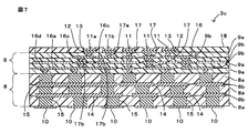
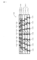
- FIG. 7 is a cross-sectional view of the multilayer wiring board 3b.
- the laminated wiring board 3c according to this embodiment differs from the laminated wiring board 3b of the second embodiment described with reference to FIGS. 4 to 6 in that each pad electrode 11, 11a, 11b and the first in-plane electrode 16a, the resin layer 9a and the wiring layer 9b are increased by one layer, and between each pad electrode 11, 11a, 11b and the first in-plane electrode 16a. This is that a flat ground electrode 16d is provided on the arranged wiring layer 9b. Since other configurations are the same as those of the multilayer wiring board 3b of the second embodiment, the description thereof is omitted by giving the same reference numerals.
- a ground electrode 16d (corresponding to the “second in-plane electrode” of the present invention) is provided as a ground wiring electrode for grounding on the wiring layer 9b one layer above the first in-plane electrode 16a.
- the heat generated when the probe card 1 is used heat transmitted from the probe pins 5, 5a, 5b
- the ground electrode 16d is also transmitted to the ground electrode 16d, thereby reducing the influence of heat on the first in-plane electrode 16a. Therefore, peeling of the first in-plane electrode 16a from the resin layer 9a can be reduced.
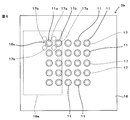
- FIG. 8 is a plan view of the laminated wiring board 3d.
- the laminated wiring board 3d according to this embodiment is different from the laminated wiring board 3b of the second embodiment described with reference to FIGS. 4 to 6, except that the first in-plane electrode 16a is as shown in FIG. In the plan view, the pad electrodes 11, 11a, 11b are arranged so as not to overlap each other. Since other configurations are the same as those of the multilayer wiring board 3b of the second embodiment, the description thereof is omitted by giving the same reference numerals.
- the first in-plane electrode 16a is arranged at the peripheral portion (in this embodiment, L-shaped) of the resin layer 9a, avoiding the central portion where the pad electrodes 11, 11a, 11b are formed. In the region immediately below the pad electrodes 11, 11a, 11b, it is easily affected by heat generated during inspection and stress from the probe pins 5, 5a, 5b. Therefore, by disposing the first in-plane electrode 16a in a plan view from the pad electrodes 11, 11a, 11b, the influence of the heat and stress described above can be suppressed, and therefore the resin layer of the first in-plane electrode 16a. Peeling from 9a can be further reduced.
- FIG. 9 is a plan view of the multilayer wiring board 3e. In FIG. 9, some via conductors 17 and 17a are not shown.
- the difference between the laminated wiring board 3e according to this embodiment and the laminated wiring board 3d of the fourth embodiment described with reference to FIG. 8 is that the shape of the first in-plane electrode 16a is different. Since other configurations are the same as those of the laminated wiring board 3d of the fourth embodiment, the description thereof is omitted by giving the same reference numerals.
- the first in-plane electrode 16a is formed over substantially the entire main surface of the resin layer 9a, but at the position overlapping the pad electrodes 11, 11a, and 11b in plan view, the through-hole 19 ( Corresponding to the “first through-hole” of the present invention).
- Each through hole 19 is formed slightly larger than the pad electrodes 11, 11a, 11b.
- FIG. 10 is a plan view of the multilayer wiring board 3e according to this example, and corresponds to FIG.
- a plurality of through holes 20 are further provided in the peripheral portion of the first in-plane electrode 16. If it does in this way, each resin of resin layer 9a located in the upper and lower sides of the 1st in-plane electrode 16a will enter into each through-hole 20, and will contact
- the present invention is not limited to the above-described embodiments, and various modifications other than those described above can be made without departing from the spirit of the invention.
- the configurations of the embodiments may be combined, such as providing the ground electrode 16d of the third embodiment between the pad electrodes 11a, 11b and the first in-plane electrode 16a.
- each via conductor 17, 17a, 17b formed in the resin laminate 9 is formed by a thin film process.
- the via hole is electrically conductive.
- the formation method can be appropriately changed, such as paste filling or via fill plating.
- the present invention can be widely applied to various probe cards used for electrical inspection of an object to be inspected.
Landscapes
- Engineering & Computer Science (AREA)
- Physics & Mathematics (AREA)
- General Physics & Mathematics (AREA)
- Manufacturing & Machinery (AREA)
- Microelectronics & Electronic Packaging (AREA)
- Production Of Multi-Layered Print Wiring Board (AREA)
- Testing Or Measuring Of Semiconductors Or The Like (AREA)
Abstract
樹脂層の積層体を有するプローブカード用積層配線基板において、配線抵抗を下げるために設けられる面積の大きい電極が、樹脂層から剥離するのを抑える。 積層配線基板3aは、コア基板8と、樹脂層9aと配線層9bとが交互に積層されて成りコア基板8に積層された樹脂積層体9と、樹脂積層体9の最表層に位置する樹脂層9a上に設けられたプローブピン接続用のパッド電極11a,11bと、樹脂積層体9の内層に位置する配線層9bに設けられた平板状の第1面内電極16aと、パッド電極11a,11bと第1面内電極16aとを接続する接続配線CLとを備え、接続配線CLは、パッド電極11a,11bと第1面内電極16aとの間の各樹脂層9aに設けられたビア導体17a,17bと、配線電極16bとを有し、ビア導体17bは、平面視でパッド電極11a,11bに重ならないようにずれて配置されている。
Description
本発明は、被検査物の電気検査に使用されるプローブカードおよびこのプローブカードが備える積層配線基板に関する。
LSIなどの半導体素子の電気検査に使用されるプローブカードでは、マザー基板の外部電極とプローブピンとの間の接続配線を形成する基板としてセラミック多層基板が広く採用されている。また、近年では、半導体素子の高集積化により、その端子数の増加や、端子の狭ピッチ化が進んでいるため、セラミック多層基板の一部の層を、微細な配線形成が容易なポリイミドなどの樹脂層に置き換えた積層配線基板が用いられるようになっている。
例えば、特許文献1に記載の積層配線基板100では、図11に示すように、複数のセラミック層101aが積層されて成るセラミック積層体101と、複数の樹脂層102aが積層されて成る樹脂積層体102とを備え、セラミック積層体101上に樹脂積層体102が積層された構造となっている。このとき、積層配線基板100の上面には、それぞれプローブピンに接続される複数の表面電極103が狭ピッチで形成される。また、積層配線基板100の下面には、各表面電極103に対応して設けられ、対応する表面電極103にそれぞれ接続された複数の裏面電極104が形成される。各裏面電極104は、マザー基板との接続用に設けられている。
また、樹脂積層体102およびセラミック積層体101の内部には、隣接する裏面電極104間のピッチが、隣接する表面電極103間のピッチよりも広くなるように、再配線構造が形成されている。
このような再配線構造を形成するに当たり、表面電極103に近い方の樹脂積層体102では、その内部に形成する配線の細線化や、隣接する配線間の距離を狭くする必要があるため、微細な配線形成が可能なポリイミド等から成る樹脂層102aで構成されている。また、比較的配線の形成スペースに余裕があるセラミック積層体101では、樹脂層102aよりも剛性が高く、線膨張係数がICウエハ等の検査媒体の線膨張係数に近いセラミック層101aで構成されている。積層配線基板100をこのように構成することで、端子数の増加や、端子間が狭ピッチ化された近年の半導体素子の電気検査を可能にしている。
ところで、この種のプローブカードは、樹脂積層体102に形成される配線パターンは微細である一方、配線抵抗が高い。そこで、従来では、大電流が流れる配線パターンの配線抵抗を下げるために、当該配線パターンの一部に面積が大きい平板状の電極(いわゆるベタ電極)を設ける場合がある。
しかしながら、電極と樹脂積層体102を形成する樹脂とは線膨張係数が異なるため、ベタ電極のように面積が大きい電極を、プローブピンに接続される表面電極103の直下に配置し、両者をビア導体などの層間接続導体を介して接続すると、プローブピンが表面電極103に押し当てられる時の応力が、ベタ電極にダイレクトに作用し、ベタ電極が樹脂層102aから剥離するおそれがある。
本発明は、上記した課題に鑑みてなされたものであり、樹脂層の積層体を有するプローブカード用積層配線基板において、配線抵抗を下げるために設けられる面積の大きい平板状の電極(いわゆるベタ電極)が、樹脂層から剥離するのを抑えることを目的とする。
上記した目的を達成するために、本発明のプローブカード用積層配線基板は、コア基板と、複数の樹脂層と複数の配線層とを有し、前記樹脂層と前記配線層とが交互に積層されて成り前記コア基板に積層された樹脂積層体と、前記樹脂積層体の最表層に位置する前記樹脂層上に設けられたプローブピン接続用のパッド電極と、前記樹脂積層体の内層に位置する所定の配線層に設けられた平板状の第1面内電極と、前記パッド電極と前記第1面内電極とを接続する接続配線とを備え、前記パッド電極と前記第1面内電極との間には、複数の樹脂層が配置され、前記接続配線は、前記パッド電極と前記第1面内電極との間の前記各樹脂層それぞれに設けられた層間接続用の複数の貫通導体と、前記パッド電極と前第1記面内電極との間の前記配線層に設けられた面内ライン電極とを有し、前記複数の貫通導体のうちの少なくとも1つは、平面視で前記パッド電極に重ならないようにずれて配置されていることを特徴としている。
この構成によると、接続配線が有する複数の貫通導体のうちの少なくとも1つは、平面視でパッド電極に重ならないようにずれて配置されるため、被検査物の検査時に、プローブピンから第1面内電極に作用する応力を低減することができ、これにより、第1面内電極の樹脂層からの剥離を低減することができる。
また、前記接続配線は、前記パッド電極から前記第1面内電極に至る経路の途中で分岐した分岐配線を有し、当該分岐配線も前記第1面内電極に接続されていてもよい。このようにすると、パッド電極と第1面内電極とを接続する接続配線全体としての配線抵抗を下げることができるため、プローブカードの使用時に接続配線に発生する熱を抑えることができる。また、接続配線での熱を抑えることで、樹脂層と接続配線の線膨張係数の違いに起因する接続配線の剥がれを低減することができる。
また、前記パッド電極と前記第1面内電極との間に配置された前記配線層に、平板状の第2面内電極が設けられていてもよい。この構成によると、プローブカードの使用時に発生する熱が、第2面内電極にも伝わることで、第1面内電極に対する熱の影響が緩和されるため、第1面内電極の樹脂層からの剥離を低減することができる。
また、前記第1面内電極は、平面視で前記パッド電極に重ならないようにずれて配置されていてもよい。パッド電極の真下の領域は、プローブピンからの応力や、プローブカード使用時の発生熱の影響が大きい。そこで、第1面内電極をパッド電極からずらすことで、これらの影響を抑えることができるため、第1面内電極の樹脂層からの剥離を低減することができる。
また、前記第1面内電極には、平面視で前記パッド電極に重なる位置に第1の透孔が設けられていてもよい。このように、パッド電極の真下に第1の透孔による電極非形成領域を形成することで、プローブピンを被検査物に押し当てたときの第1面内電極に作用する応力を緩和することができるため、第1面内電極の樹脂層からの剥離を低減することができる。また、第1の透孔には、第1面内電極の上下に位置する樹脂層の樹脂が入り込んで両者が密着する。樹脂層同士の密着強度は、第1面内電極と樹脂層との密着強度よりも強いため、第1の透孔を設けると、第1面内電極と樹脂層との密着を補強することができる。
また、前記第1面内電極には、前記第1の透孔とは異なる位置に第2の透孔がさらに設けられていてもよい。この場合、第2の透孔により、第1面内電極と樹脂層との密着がさらに補強されるため、第1面内電極の樹脂層からの剥離をさらに低減することができる。
また、上記のプローブカード用積層配線基板を、被検査物の電気検査を行うプローブカードに使用してもかまわない。この場合、第1面内電極の樹脂層からの剥離が低減されたプローブカードを提供することができる。
本発明によれば、パッド電極と平板状の第1面内電極とが接続配線により接続されるため、接続配線および第1面内電極を含む配線ラインの配線抵抗を下げることができる。また、接続配線が有する複数の貫通導体のうちの少なくとも1つは、平面視でパッド電極に重ならないようにずれて配置されるため、被検査物の検査時に、プローブピンから第1面内電極に作用する応力を低減することができ、これにより、第1面内電極の樹脂層からの剥離を低減することができる。
<第1実施形態>
本発明の第1実施形態にかかるプローブカード1について、図1~図3を参照して説明する。なお、図1はプローブカード1の断面図、図2は図1の接続配線CLを説明するための図、図3は図1の積層配線基板3aの平面図である。
本発明の第1実施形態にかかるプローブカード1について、図1~図3を参照して説明する。なお、図1はプローブカード1の断面図、図2は図1の接続配線CLを説明するための図、図3は図1の積層配線基板3aの平面図である。
この実施形態にかかるプローブカード1は、図1に示すように、マザー基板2と、該マザー基板2の一方主面に実装された積層配線基板3aと、それぞれ積層配線基板3aに接続される複数のプローブピン5,5a,5bを支持するプローブヘッド4と、プローブヘッド4を固定するカバー体21とを備え、例えば、半導体素子などの被検査物50の電気検査に使用される。
マザー基板2は、一方主面に積層配線基板3aを実装するための複数の実装電極6が形成されるとともに、他方主面に外部接続用の複数の外部電極7が形成される。ここで、各実装電極6は、マザー基板の内部に形成された配線電極30やビア導体31により所定の外部電極7に接続される。マザー基板2は、例えば、ガラスエポキシ樹脂などで形成されている。なお、各プローブピン5,5a,5bを保持するプローブヘッド4は、マザー基板2に固定されたカバー体21に固定される。
積層配線基板3aは、マザー基板2側に配置されたコア基板8と、該コア基板8に積層された樹脂積層体9とを備える。コア基板8は、複数(この実施形態では3層)のセラミック層8aと複数の配線層8bとを有し、この実施形態では、セラミック層8aと配線層8bとが交互に積層されて成る。各セラミック層8aは、例えば、ホウケイ酸系ガラスを含有するセラミック(例えば、アルミナ)を主成分とする低温同時焼成セラミック(LTCC)、高温焼成セラミック(HTCC)など、種々のセラミックで形成することができる。
樹脂積層体9は、複数の樹脂層9aと、複数の配線層9bとを有し、この実施形態では、樹脂層9aと配線層9bとが交互に積層されて成る。各樹脂層9aは、例えば、ポリイミドなどの樹脂で形成される。
コア基板8の各配線層8bには、各種配線電極14が形成されている。また、各セラミック層8aには、異なる配線層8bに形成された配線電極14同士を接続する複数のビア導体15が形成される。各ビア導体15および各配線電極14は、Cu、Ag、Al等の金属でそれぞれ形成される。配線層8bに形成される配線電極14は、例えば、上記金属(Cu、Ag、Al等)を含有する導電性ペーストを用いたスクリーン印刷などで形成することができる。
コア基板8の樹脂積層体9と反対側の主面には、マザー基板2に実装するための複数の外部接続電極10が形成され、これらの各外部接続電極10がマザー基板2に形成された所定の実装電極6にそれぞれ半田で接続される。これらの外部接続電極10は、例えば、Cu、Ag、Al等の金属で形成される。
樹脂積層体9の各配線層9bには、各種配線電極16,16a,16bが形成されている。また、樹脂積層体9の最表層に位置する樹脂層9a上には、それぞれ所定のプローブピン5,5a,5bに接続される複数のパッド電極11,11a,11bが形成される。ここで、各樹脂層9aには、異なる配線層9bに形成された配線電極16,16a,16b同士や、各パッド電極11,11a,11bと樹脂積層体9内部の配線電極16,16bとを接続する複数のビア導体17,17a,17bが形成される。
また、最上層の樹脂層9aには、樹脂積層体9の表面を保護するための絶縁被覆膜18が積層される。この絶縁被覆膜18は、各パッド電極11,11a,11bを露出させた状態で最上層の樹脂層9aに積層される。なお、この実施形態では、絶縁被覆膜18が、樹脂層9aと同様にポリイミドで形成されている。
各配線電極16,16a,16bは、例えば、所定の樹脂層9aの主面に、下地電極としてのTi膜をスパッタ等により成膜し、同じくスパッタ等によりTi膜上にCu膜を成膜する。そして、Cu膜上に、電解または無電解めっきにより、同じくCu膜を成膜することで形成することができる。また、これらの配線電極16,16a,16bは、フォトリソグラフィ加工により微細パターンに形成される。また、各パッド電極11a~11eは、例えば、Cu等で形成された下地電極12と、該下地電極12上にNi/Auめっきが施されて成る表面電極13とでそれぞれ構成されている。なお、この実施形態では、樹脂積層体9に形成される各ビア導体17,17a,17bは、ビア孔の形成後、該ビア孔内に各配線電極16,16a,16bと同時に成膜されることにより形成される。
また、各パッド電極11,11a,11bは、マザー基板2の他方主面に形成された所定の外部電極7にそれぞれ電気的に接続される。具体的には、図1に示すように、各パッド電極11,11a,11bは、それぞれ、樹脂積層体9に形成された配線電極16,16a,16bおよびビア導体17,17a,17b、コア基板8に形成された配線電極14およびビア導体15、マザー基板2に形成された配線電極30およびビア導体31を介して所定の外部電極7に接続される。
なお、コア基板8に形成された各配線電極14は、スクリーン印刷などで形成されるため、厚膜パターンとなる。一方、樹脂積層体9に形成された各配線電極16,16a,16bは、スパッタ等で成膜されるため、薄膜パターンとなる。さらに、各パッド電極11、11a、11bの狭ピッチ化にともなって、一部の配線電極16,16bでは、フォトリソグラフィ加工で細線化される。そのため、薄くかつ細く形成された配線電極16,16bは、コア基板8に形成された配線電極14よりも配線抵抗が高い。そこで、この実施形態では、比較的大電流が流れる電源供給用のプローブピン5a,5bに接続される樹脂積層体9内の配線経路に、面積が大きい平板状の第1面内電極16a(いわゆる、ベタ電極)が設けられている。なお、本実施形態において、この第1面内電極16aは、電源配線用のベタ電極である。
この実施形態では、第1面内電極16aは、図1に示すように、最下層の配線層9b(上から2番目の樹脂層9aと3番目の樹脂層9aとの間に配置された配線層9b)に設けられる。これらのパッド電極11a,11bと第1面内電極16aとの間には、2つの樹脂層9aと1つの配線層9bとが介在し、両樹脂層9aそれぞれに設けられた複数のビア導体17a,17bと、配線層9bに設けられた配線電極16bとにより、両パッド電極11a,11bと第1面内電極16aとを接続する2つの接続配線CLが形成されている。
ところで、樹脂積層体9に形成された配線電極16,16a,16bと、樹脂層9aとは線膨張係数が異なるため、特に、第1面内電極16aのように、面積の大きいベタ電極は、プローブカード1の使用時に発生する熱などにより樹脂層9aから剥離し易い。さらに、プローブカード1の使用時には、各プローブピン5a~5eが頻繁に被検査物に押し当てられるため、このときの応力が第1面内電極16aに作用すると、樹脂層9aからの剥離を助長するおそれがある。そこで、この実施形態では、第1面内電極16aの樹脂層9aからの剥離を低減するために、接続配線CLの構造が工夫されている。
パッド電極11aを例として具体的に説明すると、図2に示すように、接続配線CLは、最上層の樹脂層9aを貫通して設けられ、上端面が電源用のパッド電極11aに接続されたビア導体17aと、このビア導体17aの一つ下層の樹脂層9aを貫通して設けられて下端面が第1面内電極16aに接続されたビア導体17bと、これらのビア導体17aとビア導体17bとを接続する配線電極16bとを有する。この配線電極16bは、両ビア導体17a,17bが設けられた樹脂層9aに挟まれた配線層9bに形成される。
また、図3に示すように、一方のビア導体17aは、パッド電極11aに直接接続されるため、平面視で接続先のパッド電極11aに重なる位置に配置される。これに対して、他方のビア導体17bは、配線電極16bにより引き出されて、平面視でパッド電極11aに重ならないようにずれて配置される。なお、もう一つのパッド電極11bと第1面内電極16aとを接続する接続配線CLも同様の構成である。この構成によると、パッド電極11aと第1面内電極16aとをビア導体で直線的に接続する構成と比較して、検査時にプローブピン5,5a,5bが被検査物50に押し当てられることに起因する第1面内電極16aへの応力が緩和される。ここで、接続配線CLを構成する2つのビア導体17a,17bそれぞれが、本発明の「貫通導体」に相当し、両ビア導体17a,17bを接続する配線電極16bが本発明の「面内ライン電極」に相当する。
なお、パッド電極11aと第1面内電極16aとの間に介在する樹脂層9aは、2層以上であってもよい。この場合、接続配線CLは、間に介在する樹脂層9aの数の分だけ、ビア導体を有する構成となるが、この場合は、各ビア導体のうちの少なくとも1つを平面視でパッド電極11aと重ならないようにずらして配置すればよい。
したがって、上記した実施形態によれば、接続配線CLが有する2つのビア導体17a,17bのうちの一方のビア導体17bは、平面視でパッド電極11aに重ならないようにずれて配置されるため、被検査物50の検査時に、プローブピン5,5a,5bから第1面内電極16aに作用する応力を低減することができる。そのため、第1面内電極16aの樹脂層9aからの剥離を低減することができる。
また、プローブカード1の使用時には、プローブピン5a付近(例えば、プローブピン5aとパッド電極11aとの接続部)で発熱する。ここで、接続配線CLの第1面内電極16aに接続する部分であるビア導体17bは、配線電極16により引き出されて、平面視でパッド電極11aと重ならないようにずれて配置されているため、第1面内電極16aとビア導体17bとの接続部の温度上昇を低減することができる。
<第2実施形態>
本発明の第2実施形態にかかる積層配線基板3bについて、図4~6を参照して説明する。なお、図4は積層配線基板3bの断面図、図5は接続配線CL1を説明するための図、図6は積層配線基板3bの平面図である。
本発明の第2実施形態にかかる積層配線基板3bについて、図4~6を参照して説明する。なお、図4は積層配線基板3bの断面図、図5は接続配線CL1を説明するための図、図6は積層配線基板3bの平面図である。
この実施形態にかかる積層配線基板3bが、図1~図3を参照して説明した第1実施形態の積層配線基板3aと異なるところは、図4~図6に示すように、2つの接続配線CL1それぞれは、パッド電極11a,11bから第1面内電極16aに至る経路の途中で分岐した分岐配線CLaを有し、該分岐配線CLaも第1面内電極16aに接続されていることである。その他の構成は第1実施形態の積層配線基板3aと同じであるため、同一符号を付すことにより説明を省略する。
パッド電極11aを例として具体的に説明すると、接続配線CL1は、図5に示すように、最上層の樹脂層9aに設けられたビア導体17aと、このビア導体17aの一つ下層の樹脂層9aに設けられて第1面内電極16aにそれぞれ接続された2つのビア導体17bと、上層側のビア導体17aと下層側のビア導体17bとを接続する配線電極16cとを有する。配線電極16cは、上層側のビア導体17aと下層側の2つのビア導体17bのうちの一方とを接続する配線経路16c1と、上層側のビア導体17aと下層側の2つのビア導体17bのうちの他方とを接続する配線経路16c2とで構成される。そして、配線経路16c2と他方のビア導体17bとにより分岐配線CLaが形成される。
また、下層側の両ビア導体17bそれぞれは、図6に示すように、第1実施形態の積層配線基板3aと同様、平面視でパッド電極11aに重ならないようにずれて配置される。パッド電極11bに接続する接続配線CL1も同様の構成である。
この構成によると、パッド電極11a,11bと第1面内電極16aとを接続する経路が増えるため、接続配線CL1全体としての配線抵抗を下げることができる。
<第3実施形態>
本発明の第3実施形態にかかる積層配線基板3cについて、図7を参照して説明する。なお、図7は積層配線基板3bの断面図である。
本発明の第3実施形態にかかる積層配線基板3cについて、図7を参照して説明する。なお、図7は積層配線基板3bの断面図である。
この実施形態にかかる積層配線基板3cが、図4~図6を参照して説明した第2実施形態の積層配線基板3bと異なるところは、図7に示すように、各パッド電極11,11a,11bと第1面内電極16aとの間に配置される樹脂層9aと配線層9bとが1層ずつ多いことと、各パッド電極11,11a,11bと第1面内電極16aとの間に配置された配線層9bに、平板状のグランド電極16dが設けられていることである。その他の構成は、第2実施形態の積層配線基板3bと同じであるため、同一符号を付すことにより説明を省略する。
この場合、第1面内電極16aの一つ上層の配線層9bに、接地用のグランド配線電極として、グランド電極16d(本発明の「第2面内電極」に相当)が設けられる。この構成によると、プローブカード1の使用時に発生する熱(プローブピン5,5a,5b側から伝わる熱)が、グランド電極16dにも伝わることで、第1面内電極16aに対する熱の影響が緩和されるため、第1面内電極16aの樹脂層9aからの剥離を低減することができる。
<第4実施形態>
本発明の第4実施形態にかかる積層配線基板3dについて、図8を参照して説明する。なお、図8は積層配線基板3dの平面図である。
本発明の第4実施形態にかかる積層配線基板3dについて、図8を参照して説明する。なお、図8は積層配線基板3dの平面図である。
この実施形態にかかる積層配線基板3dが、図4~図6を参照して説明した第2実施形態の積層配線基板3bと異なるところは、図8に示すように、第1面内電極16aが、平面視で各パッド電極11,11a,11bに重ならないようにずれて配置されていることである。その他の構成は、第2実施形態の積層配線基板3bと同じであるため、同一符号を付すことにより説明を省略する。
この場合、第1面内電極16aは、各パッド電極11,11a,11bが形成される中央部を避けて、樹脂層9aの周縁部(この実施形態では、L字状)に配置される。パッド電極11,11a,11bの真下の領域では、検査時に発生する熱やプローブピン5,5a,5bからの応力の影響を受けやすい。そこで、第1面内電極16aをパッド電極11,11a,11bから平面視でずらして配置することで、上述の熱や応力の影響を抑えることができるため、第1面内電極16aの樹脂層9aからの剥離をさらに低減することができる。
<第5実施形態>
本発明の第5実施形態にかかる積層配線基板3eについて、図9を参照して説明する。なお、図9は積層配線基板3eの平面図である。また、図9では一部のビア導体17,17aを図示省略している。
本発明の第5実施形態にかかる積層配線基板3eについて、図9を参照して説明する。なお、図9は積層配線基板3eの平面図である。また、図9では一部のビア導体17,17aを図示省略している。
この実施形態にかかる積層配線基板3eが、図8を参照して説明した第4実施形態の積層配線基板3dと異なるところは、第1面内電極16aの形状が異なることである。その他の構成は、第4実施形態の積層配線基板3dと同じであるため、同一符号を付すことにより説明を省略する。
この場合、第1面内電極16aは、樹脂層9aの主面上の略全面に渡って形成されるが、各パッド電極11,11a,11bと平面視で重なる位置には、透孔19(本発明の「第1の透孔」に相当)が設けられる。各透孔19は、パッド電極11,11a,11bよりも若干大きく形成される。この構成によると、第1面内電極16aが大きくなるため、接続配線CL1および第1面内電極16aを含む電源供給用の配線ラインの配線抵抗をさらに下げることができる。また、第1面内電極16aの各パッド電極11,11a,11bの真下の領域には各透孔19が設けられるため、プローブピン5,5a、5b付近で発生する熱や、応力の影響を軽減することができる。
(第1面内電極の変形例)
次に、図10を参照して、第5実施形態の第1面内電極16aの変形例について説明する。なお、図10は、本例にかかる積層配線基板3eの平面図であり、図9に対応する図である。
次に、図10を参照して、第5実施形態の第1面内電極16aの変形例について説明する。なお、図10は、本例にかかる積層配線基板3eの平面図であり、図9に対応する図である。
この場合、第1面内電極16の周縁部に複数の透孔20(本発明の「第2の透孔」に相当)がさらに設けられる。このようにすると、第1面内電極16aの上下に位置する樹脂層9aそれぞれの樹脂が各透孔20に入り込んで密着する。樹脂同士の密着強度は、樹脂と第1面内電極16との密着強度よりも強いため、第1面内電極16aと樹脂層9aとの密着が補強される。したがって、第1面内電極16aの樹脂層9aからの剥離をさらに低減することができる。
なお、本発明は上記した各実施形態に限定されるものではなく、その趣旨を逸脱しない限りにおいて、上記したもの以外に種々の変更を行なうことが可能である。例えば、第4実施形態において、パッド電極11a,11bと第1面内電極16aとの間に、第3実施形態のグランド電極16dを設けるなど、各実施形態の構成を組合わせてもかまわない。
また、上記した各実施形態では、樹脂積層体9に形成される各ビア導体17,17a,17bが、薄膜プロセスで形成される場合について説明したが、例えば、ビア孔(貫通孔)に導電性ペースト充填したり、ビアフィルめっきするなど、その形成方法は適宜変更可能である。
本発明は、被検査物の電気検査に使用される種々のプローブカードに広く適用することができる。
1 プローブカード
3a~3e 積層配線基板
5,5a,5b プローブピン
8 コア基板
9 樹脂積層体
9a 樹脂層
9b 配線層
11,11a,11b パッド電極
16a 第1面内電極
16b,16c 配線電極(面内ライン電極)
16d グランド電極(第2面内電極)
17a,17b ビア導体(貫通導体)
19 透孔(第1の透孔)
20 透孔(第2の透孔)
CL,CL1 接続配線
CLa 分岐配線
3a~3e 積層配線基板
5,5a,5b プローブピン
8 コア基板
9 樹脂積層体
9a 樹脂層
9b 配線層
11,11a,11b パッド電極
16a 第1面内電極
16b,16c 配線電極(面内ライン電極)
16d グランド電極(第2面内電極)
17a,17b ビア導体(貫通導体)
19 透孔(第1の透孔)
20 透孔(第2の透孔)
CL,CL1 接続配線
CLa 分岐配線
Claims (7)
- コア基板と、
複数の樹脂層と複数の配線層とを有し、前記樹脂層と前記配線層とが交互に積層されて成り前記コア基板に積層された樹脂積層体と、
前記樹脂積層体の最表層に位置する前記樹脂層上に設けられたプローブピン接続用のパッド電極と、
前記樹脂積層体の内層に位置する所定の配線層に設けられた平板状の第1面内電極と、
前記パッド電極と前記第1面内電極とを接続する接続配線とを備え、
前記パッド電極と前記第1面内電極との間には、複数の樹脂層が配置され、
前記接続配線は、
前記パッド電極と前記第1面内電極との間の前記各樹脂層それぞれに設けられた層間接続用の複数の貫通導体と、前記パッド電極と前第1記面内電極との間の前記配線層に設けられた面内ライン電極とを有し、
前記複数の貫通導体のうちの少なくとも1つは、平面視で前記パッド電極に重ならないようにずれて配置されていることを特徴とするプローブカード用積層配線基板。 - 前記接続配線は、前記パッド電極から前記第1面内電極に至る経路の途中で分岐した分岐配線を有し、当該分岐配線も前記第1面内電極に接続されていることを特徴とする請求項1に記載のプローブカード用積層配線基板。
- 前記パッド電極と前記第1面内電極との間に配置された前記配線層に、平板状の第2面内電極が設けられていることを特徴とする請求項1または2に記載のプローブカード用積層配線基板。
- 前記第1面内電極は、平面視で前記パッド電極に重ならないようにずれて配置されていることを特徴とする請求項1ないし3のいずれかに記載のプローブカード用積層配線基板。
- 前記第1面内電極には、平面視で前記パッド電極に重なる位置に第1の透孔が設けられていることを特徴とする請求項1ないし3のいずれかに記載のプローブカード用積層配線基板。
- 前記第1面内電極には、前記第1の透孔とは異なる位置に第2の透孔がさらに設けられていることを特徴とする請求項5に記載のプローブカード用積層配線基板。
- 請求項1ないし6のいずれかに記載のプローブカード用積層配線基板を備え、被検査物の電気検査を行うことを特徴とするプローブカード。
Applications Claiming Priority (2)
| Application Number | Priority Date | Filing Date | Title |
|---|---|---|---|
| JP2015-005922 | 2015-01-15 | ||
| JP2015005922 | 2015-01-15 |
Publications (1)
| Publication Number | Publication Date |
|---|---|
| WO2016114170A1 true WO2016114170A1 (ja) | 2016-07-21 |
Family
ID=56405717
Family Applications (1)
| Application Number | Title | Priority Date | Filing Date |
|---|---|---|---|
| PCT/JP2016/050100 Ceased WO2016114170A1 (ja) | 2015-01-15 | 2016-01-05 | プローブカードおよびこのプローブカードが備える積層配線基板 |
Country Status (1)
| Country | Link |
|---|---|
| WO (1) | WO2016114170A1 (ja) |
Cited By (1)
| Publication number | Priority date | Publication date | Assignee | Title |
|---|---|---|---|---|
| TWI698648B (zh) * | 2019-08-29 | 2020-07-11 | 中華精測科技股份有限公司 | 高頻測試裝置及其信號傳輸模組 |
Citations (5)
| Publication number | Priority date | Publication date | Assignee | Title |
|---|---|---|---|---|
| JP2000101237A (ja) * | 1998-09-18 | 2000-04-07 | Fujitsu Ltd | ビルドアップ基板 |
| JP2002185141A (ja) * | 2000-12-15 | 2002-06-28 | Ibiden Co Ltd | 多層プリント配線板 |
| JP2008060208A (ja) * | 2006-08-30 | 2008-03-13 | Kyocera Corp | 多層配線基板およびそれを用いたプローブカード |
| JP2009092581A (ja) * | 2007-10-11 | 2009-04-30 | Ngk Spark Plug Co Ltd | 電子部品検査装置用配線基板 |
| JP2011228427A (ja) * | 2010-04-19 | 2011-11-10 | Kyocera Corp | プローブカードおよびプローブ装置 |
-
2016
- 2016-01-05 WO PCT/JP2016/050100 patent/WO2016114170A1/ja not_active Ceased
Patent Citations (5)
| Publication number | Priority date | Publication date | Assignee | Title |
|---|---|---|---|---|
| JP2000101237A (ja) * | 1998-09-18 | 2000-04-07 | Fujitsu Ltd | ビルドアップ基板 |
| JP2002185141A (ja) * | 2000-12-15 | 2002-06-28 | Ibiden Co Ltd | 多層プリント配線板 |
| JP2008060208A (ja) * | 2006-08-30 | 2008-03-13 | Kyocera Corp | 多層配線基板およびそれを用いたプローブカード |
| JP2009092581A (ja) * | 2007-10-11 | 2009-04-30 | Ngk Spark Plug Co Ltd | 電子部品検査装置用配線基板 |
| JP2011228427A (ja) * | 2010-04-19 | 2011-11-10 | Kyocera Corp | プローブカードおよびプローブ装置 |
Cited By (1)
| Publication number | Priority date | Publication date | Assignee | Title |
|---|---|---|---|---|
| TWI698648B (zh) * | 2019-08-29 | 2020-07-11 | 中華精測科技股份有限公司 | 高頻測試裝置及其信號傳輸模組 |
Similar Documents
| Publication | Publication Date | Title |
|---|---|---|
| JP6304263B2 (ja) | 積層配線基板およびこれを備える検査装置 | |
| CN108713354B (zh) | 探针卡用层叠布线基板以及具备它的探针卡 | |
| WO2016075863A1 (ja) | 配線回路基板、半導体装置、配線回路基板の製造方法、半導体装置の製造方法 | |
| US20160313393A1 (en) | Multilayer circuit board and tester including the same | |
| CN104902678B (zh) | 柔性印刷电路板及其制作方法 | |
| JP5445985B2 (ja) | プローブカード及びその製造方法 | |
| JP6226168B2 (ja) | 多層配線板 | |
| KR102229729B1 (ko) | 검사장치용 배선기판 | |
| JP6531845B2 (ja) | 多層配線基板およびこれを備えるプローブカード | |
| JPWO2016024534A1 (ja) | プローブカードおよびこのプローブカードが備える積層配線基板 | |
| JP6589990B2 (ja) | プローブカード用積層配線基板およびこれを備えるプローブカード | |
| JP2016219730A (ja) | 電子部品内蔵基板及びその製造方法と電子装置 | |
| JP2013083620A (ja) | プローブカード及びその製造方法 | |
| JP6847780B2 (ja) | 回路基板およびプローブカード | |
| KR102368837B1 (ko) | 배선기판 | |
| US20140116762A1 (en) | Wiring board and mounting structure using the same | |
| WO2016114170A1 (ja) | プローブカードおよびこのプローブカードが備える積層配線基板 | |
| JP2019049498A (ja) | 電子部品検査装置用配線基板 | |
| JP6683533B2 (ja) | 配線基板 | |
| JP2017175111A (ja) | 回路基板およびプローブカード | |
| TWI782100B (zh) | 貫通電極基板及使用有貫通電極基板之半導體裝置 | |
| JP6235955B2 (ja) | 多層セラミック配線基板 | |
| JP6225057B2 (ja) | 多層セラミック配線基板 | |
| JP2009122123A (ja) | コンタクトプローブ | |
| JPS61166198A (ja) | 多層配線基板 |
Legal Events
| Date | Code | Title | Description |
|---|---|---|---|
| 121 | Ep: the epo has been informed by wipo that ep was designated in this application |
Ref document number: 16737241 Country of ref document: EP Kind code of ref document: A1 |
|
| NENP | Non-entry into the national phase |
Ref country code: DE |
|
| NENP | Non-entry into the national phase |
Ref country code: JP |
|
| 122 | Ep: pct application non-entry in european phase |
Ref document number: 16737241 Country of ref document: EP Kind code of ref document: A1 |