WO2016110906A1 - 電子デバイス用エピタキシャル基板、電子デバイス、電子デバイス用エピタキシャル基板の製造方法、並びに電子デバイスの製造方法 - Google Patents
電子デバイス用エピタキシャル基板、電子デバイス、電子デバイス用エピタキシャル基板の製造方法、並びに電子デバイスの製造方法 Download PDFInfo
- Publication number
- WO2016110906A1 WO2016110906A1 PCT/JP2015/006313 JP2015006313W WO2016110906A1 WO 2016110906 A1 WO2016110906 A1 WO 2016110906A1 JP 2015006313 W JP2015006313 W JP 2015006313W WO 2016110906 A1 WO2016110906 A1 WO 2016110906A1
- Authority
- WO
- WIPO (PCT)
- Prior art keywords
- layer
- electronic device
- epitaxial substrate
- aln initial
- buffer layer
- Prior art date
- Legal status (The legal status is an assumption and is not a legal conclusion. Google has not performed a legal analysis and makes no representation as to the accuracy of the status listed.)
- Ceased
Links
Images



Classifications
-
- H—ELECTRICITY
- H10—SEMICONDUCTOR DEVICES; ELECTRIC SOLID-STATE DEVICES NOT OTHERWISE PROVIDED FOR
- H10P—GENERIC PROCESSES OR APPARATUS FOR THE MANUFACTURE OR TREATMENT OF DEVICES COVERED BY CLASS H10
- H10P14/00—Formation of materials, e.g. in the shape of layers or pillars
- H10P14/20—Formation of materials, e.g. in the shape of layers or pillars of semiconductor materials
- H10P14/32—Formation of materials, e.g. in the shape of layers or pillars of semiconductor materials characterised by intermediate layers between substrates and deposited layers
- H10P14/3242—Structure
- H10P14/3256—Microstructure
-
- H—ELECTRICITY
- H10—SEMICONDUCTOR DEVICES; ELECTRIC SOLID-STATE DEVICES NOT OTHERWISE PROVIDED FOR
- H10P—GENERIC PROCESSES OR APPARATUS FOR THE MANUFACTURE OR TREATMENT OF DEVICES COVERED BY CLASS H10
- H10P14/00—Formation of materials, e.g. in the shape of layers or pillars
- H10P14/60—Formation of materials, e.g. in the shape of layers or pillars of insulating materials
- H10P14/63—Formation of materials, e.g. in the shape of layers or pillars of insulating materials characterised by the formation processes
- H10P14/6326—Deposition processes
- H10P14/6349—Deposition of epitaxial materials
-
- C—CHEMISTRY; METALLURGY
- C30—CRYSTAL GROWTH
- C30B—SINGLE-CRYSTAL GROWTH; UNIDIRECTIONAL SOLIDIFICATION OF EUTECTIC MATERIAL OR UNIDIRECTIONAL DEMIXING OF EUTECTOID MATERIAL; REFINING BY ZONE-MELTING OF MATERIAL; PRODUCTION OF A HOMOGENEOUS POLYCRYSTALLINE MATERIAL WITH DEFINED STRUCTURE; SINGLE CRYSTALS OR HOMOGENEOUS POLYCRYSTALLINE MATERIAL WITH DEFINED STRUCTURE; AFTER-TREATMENT OF SINGLE CRYSTALS OR A HOMOGENEOUS POLYCRYSTALLINE MATERIAL WITH DEFINED STRUCTURE; APPARATUS THEREFOR
- C30B25/00—Single-crystal growth by chemical reaction of reactive gases, e.g. chemical vapour-deposition growth
- C30B25/02—Epitaxial-layer growth
- C30B25/18—Epitaxial-layer growth characterised by the substrate
- C30B25/183—Epitaxial-layer growth characterised by the substrate being provided with a buffer layer, e.g. a lattice matching layer
-
- C—CHEMISTRY; METALLURGY
- C30—CRYSTAL GROWTH
- C30B—SINGLE-CRYSTAL GROWTH; UNIDIRECTIONAL SOLIDIFICATION OF EUTECTIC MATERIAL OR UNIDIRECTIONAL DEMIXING OF EUTECTOID MATERIAL; REFINING BY ZONE-MELTING OF MATERIAL; PRODUCTION OF A HOMOGENEOUS POLYCRYSTALLINE MATERIAL WITH DEFINED STRUCTURE; SINGLE CRYSTALS OR HOMOGENEOUS POLYCRYSTALLINE MATERIAL WITH DEFINED STRUCTURE; AFTER-TREATMENT OF SINGLE CRYSTALS OR A HOMOGENEOUS POLYCRYSTALLINE MATERIAL WITH DEFINED STRUCTURE; APPARATUS THEREFOR
- C30B29/00—Single crystals or homogeneous polycrystalline material with defined structure characterised by the material or by their shape
- C30B29/10—Inorganic compounds or compositions
- C30B29/40—AIIIBV compounds wherein A is B, Al, Ga, In or Tl and B is N, P, As, Sb or Bi
- C30B29/403—AIII-nitrides
-
- H—ELECTRICITY
- H10—SEMICONDUCTOR DEVICES; ELECTRIC SOLID-STATE DEVICES NOT OTHERWISE PROVIDED FOR
- H10D—INORGANIC ELECTRIC SEMICONDUCTOR DEVICES
- H10D30/00—Field-effect transistors [FET]
- H10D30/40—FETs having zero-dimensional [0D], one-dimensional [1D] or two-dimensional [2D] charge carrier gas channels
- H10D30/47—FETs having zero-dimensional [0D], one-dimensional [1D] or two-dimensional [2D] charge carrier gas channels having two-dimensional [2D] charge carrier gas channels, e.g. nanoribbon FETs or high electron mobility transistors [HEMT]
-
- H—ELECTRICITY
- H10—SEMICONDUCTOR DEVICES; ELECTRIC SOLID-STATE DEVICES NOT OTHERWISE PROVIDED FOR
- H10D—INORGANIC ELECTRIC SEMICONDUCTOR DEVICES
- H10D30/00—Field-effect transistors [FET]
- H10D30/40—FETs having zero-dimensional [0D], one-dimensional [1D] or two-dimensional [2D] charge carrier gas channels
- H10D30/47—FETs having zero-dimensional [0D], one-dimensional [1D] or two-dimensional [2D] charge carrier gas channels having two-dimensional [2D] charge carrier gas channels, e.g. nanoribbon FETs or high electron mobility transistors [HEMT]
- H10D30/471—High electron mobility transistors [HEMT] or high hole mobility transistors [HHMT]
- H10D30/475—High electron mobility transistors [HEMT] or high hole mobility transistors [HHMT] having wider bandgap layer formed on top of lower bandgap active layer, e.g. undoped barrier HEMTs such as i-AlGaN/GaN HEMTs
-
- H—ELECTRICITY
- H10—SEMICONDUCTOR DEVICES; ELECTRIC SOLID-STATE DEVICES NOT OTHERWISE PROVIDED FOR
- H10D—INORGANIC ELECTRIC SEMICONDUCTOR DEVICES
- H10D30/00—Field-effect transistors [FET]
- H10D30/60—Insulated-gate field-effect transistors [IGFET]
-
- H—ELECTRICITY
- H10—SEMICONDUCTOR DEVICES; ELECTRIC SOLID-STATE DEVICES NOT OTHERWISE PROVIDED FOR
- H10D—INORGANIC ELECTRIC SEMICONDUCTOR DEVICES
- H10D30/00—Field-effect transistors [FET]
- H10D30/80—FETs having rectifying junction gate electrodes
- H10D30/87—FETs having Schottky gate electrodes, e.g. metal-semiconductor FETs [MESFET]
-
- H—ELECTRICITY
- H10—SEMICONDUCTOR DEVICES; ELECTRIC SOLID-STATE DEVICES NOT OTHERWISE PROVIDED FOR
- H10P—GENERIC PROCESSES OR APPARATUS FOR THE MANUFACTURE OR TREATMENT OF DEVICES COVERED BY CLASS H10
- H10P14/00—Formation of materials, e.g. in the shape of layers or pillars
- H10P14/20—Formation of materials, e.g. in the shape of layers or pillars of semiconductor materials
- H10P14/29—Formation of materials, e.g. in the shape of layers or pillars of semiconductor materials characterised by the substrates
- H10P14/2901—Materials
- H10P14/2902—Materials being Group IVA materials
- H10P14/2905—Silicon, silicon germanium or germanium
-
- H—ELECTRICITY
- H10—SEMICONDUCTOR DEVICES; ELECTRIC SOLID-STATE DEVICES NOT OTHERWISE PROVIDED FOR
- H10P—GENERIC PROCESSES OR APPARATUS FOR THE MANUFACTURE OR TREATMENT OF DEVICES COVERED BY CLASS H10
- H10P14/00—Formation of materials, e.g. in the shape of layers or pillars
- H10P14/20—Formation of materials, e.g. in the shape of layers or pillars of semiconductor materials
- H10P14/32—Formation of materials, e.g. in the shape of layers or pillars of semiconductor materials characterised by intermediate layers between substrates and deposited layers
- H10P14/3202—Materials thereof
- H10P14/3214—Materials thereof being Group IIIA-VA semiconductors
- H10P14/3216—Nitrides
-
- H—ELECTRICITY
- H10—SEMICONDUCTOR DEVICES; ELECTRIC SOLID-STATE DEVICES NOT OTHERWISE PROVIDED FOR
- H10P—GENERIC PROCESSES OR APPARATUS FOR THE MANUFACTURE OR TREATMENT OF DEVICES COVERED BY CLASS H10
- H10P14/00—Formation of materials, e.g. in the shape of layers or pillars
- H10P14/20—Formation of materials, e.g. in the shape of layers or pillars of semiconductor materials
- H10P14/32—Formation of materials, e.g. in the shape of layers or pillars of semiconductor materials characterised by intermediate layers between substrates and deposited layers
- H10P14/3242—Structure
- H10P14/3244—Layer structure
- H10P14/3251—Layer structure consisting of three or more layers
- H10P14/3252—Alternating layers, e.g. superlattice
-
- H—ELECTRICITY
- H10—SEMICONDUCTOR DEVICES; ELECTRIC SOLID-STATE DEVICES NOT OTHERWISE PROVIDED FOR
- H10P—GENERIC PROCESSES OR APPARATUS FOR THE MANUFACTURE OR TREATMENT OF DEVICES COVERED BY CLASS H10
- H10P14/00—Formation of materials, e.g. in the shape of layers or pillars
- H10P14/20—Formation of materials, e.g. in the shape of layers or pillars of semiconductor materials
- H10P14/34—Deposited materials, e.g. layers
- H10P14/3402—Deposited materials, e.g. layers characterised by the chemical composition
- H10P14/3414—Deposited materials, e.g. layers characterised by the chemical composition being group IIIA-VIA materials
- H10P14/3416—Nitrides
-
- H—ELECTRICITY
- H10—SEMICONDUCTOR DEVICES; ELECTRIC SOLID-STATE DEVICES NOT OTHERWISE PROVIDED FOR
- H10D—INORGANIC ELECTRIC SEMICONDUCTOR DEVICES
- H10D62/00—Semiconductor bodies, or regions thereof, of devices having potential barriers
- H10D62/80—Semiconductor bodies, or regions thereof, of devices having potential barriers characterised by the materials
- H10D62/85—Semiconductor bodies, or regions thereof, of devices having potential barriers characterised by the materials being Group III-V materials, e.g. GaAs
- H10D62/8503—Nitride Group III-V materials, e.g. AlN or GaN
Definitions
- the present invention relates to an electronic device epitaxial substrate, an electronic device, a method for manufacturing an electronic device epitaxial substrate, and a method for manufacturing an electronic device.
- Patent Document 1 touches the roughness of the AlN layer as an initial layer, and the surface roughness Ra of the silicon substrate in contact with the AlN layer is set to 0.2 to 1 nm, so that the group III nitride grown above the surface roughness Ra.
- the improvement of crystallinity of a physical semiconductor is disclosed.
- Patent Document 1 does not mention electrical characteristics.
- the present inventors have studied the electrical characteristics of the epitaxial wafer as described above, and there is a correlation between the V pits of the buffer layer structure and the longitudinal leakage current characteristics. It has been found that the directional leakage current decreases. However, there is room for study on how to suppress the V pits of the buffer layer structure.
- the present invention has been made in view of the above problems, and provides an epitaxial substrate for an electronic device that can suppress V pits in a buffer layer structure and improve current leakage characteristics when an electronic device is fabricated.
- the purpose is to do.
- the present invention provides an epitaxial substrate for an electronic device comprising a Si-based substrate, an AlN initial layer provided on the Si-based substrate, and a buffer layer provided on the AlN initial layer. And the roughness Sa of the surface by the side of the said buffer layer of the said AlN initial layer is 4 nm or more,
- the epitaxial substrate for electronic devices characterized by the above-mentioned is provided.
- the roughness Sa on the surface of the AlN initial layer on the buffer layer side is 4 nm or more, V pits in the buffer layer structure formed on the AlN initial layer are suppressed, and the vertical length when the electronic device is manufactured is reduced.
- Directional leakage current characteristics can be improved.
- the surface roughness Sa of the AlN initial layer on the buffer layer side is preferably 8 nm or less.
- the roughness Sa on the surface of the AlN initial layer on the buffer layer side is 8 nm or less, V pits of the buffer layer structure formed on the AlN initial layer can be reliably suppressed.
- the buffer layer includes an Al z Ga 1-z N (0 ⁇ z ⁇ 1) layer in contact with the AlN initial layer, and the Al z Ga 1-z N (0 ⁇ z ⁇ 1) layer It is preferable that the roughness Sa on the surface opposite to the AlN initial layer is 0.6 nm or less. Thus, if the roughness Sa of the surface of the Al z Ga 1-z N layer opposite to the AlN initial layer is 0.6 nm or less, the longitudinal leakage current characteristics when the electronic device is fabricated are effectively improved. can do.
- the buffer layer is in contact with the Al z Ga 1-z N (0 ⁇ z ⁇ 1) layer, and the Al x Ga 1-x N (0 ⁇ x ⁇ 1) layer and the Al y Ga 1 ⁇ a multilayer film in which y N (0 ⁇ y ⁇ x) layers are alternately stacked, and the roughness of the surface of the multilayer film on the side opposite to the Al z Ga 1-z N (0 ⁇ z ⁇ 1) layer It is preferable that Sa is 0.3 nm or less. Thus, if the roughness Sa on the surface opposite to the Al z Ga 1-z N (0 ⁇ z ⁇ 1) layer of the multilayer film is 0.3 nm or less, the longitudinal leakage current when the electronic device is manufactured The characteristics can be improved more effectively.
- a channel layer provided on the buffer layer it is preferable to further include a channel layer provided on the buffer layer, a barrier layer provided on the channel layer, and a cap layer provided on the barrier layer.
- a channel layer provided on the buffer layer a barrier layer provided on the channel layer, and a cap layer provided on the barrier layer.
- Such a configuration can be suitably used as an epitaxial substrate for electronic devices.
- an electronic device manufactured using the above-described epitaxial substrate for an electronic device, wherein an electrode is provided on the epitaxial substrate for an electronic device. provide.
- Such an electronic device can suppress the V pits of the buffer layer structure formed on the AlN initial layer and improve the vertical leakage current characteristics.
- the present invention also includes a step of forming an AlN initial layer on a Si-based substrate, a step of forming a buffer layer on the AlN initial layer, a step of forming a channel layer on the buffer layer, and the channel layer.
- a method for manufacturing an epitaxial substrate for an electronic device is provided.
- V pits in the buffer layer structure formed on the AlN initial layer are suppressed, and the longitudinal leakage current characteristics when the electronic device is manufactured are improved.
- An epitaxial substrate for electronic devices can be manufactured.
- the present invention also includes a step of forming an AlN initial layer on a Si-based substrate, a step of forming a buffer layer on the AlN initial layer, a step of forming a channel layer on the buffer layer, and the channel layer.
- roughness Sa is 4 nm or more.
- Such an electronic device manufacturing method can manufacture an electronic device in which the V pits of the buffer layer structure formed on the AlN initial layer are suppressed and the vertical leakage current characteristics are improved.
- the present invention it is possible to suppress the V pits of the buffer layer structure formed on the AlN initial layer and improve the vertical leakage current characteristics when an electronic device is manufactured.
- the present inventors examined the electrical characteristics of an epitaxial wafer obtained by epitaxially growing a GaN film on a Si substrate.
- the one with the poor vertical leakage current characteristics was selected arbitrarily, the one with the good one was divided, each wafer was divided into two, and the vertical leakage current characteristic evaluation was performed on one of the two divided wafers, and the other two divided wafers Failure analysis (cross-sectional observation) was performed.
- the failure analysis was performed by cleaving the epitaxial wafer and observing the V pits of the buffer layer structure with a cross-section of SEM magnification of 25k.
- the V pit of the buffer layer structure will be described.
- each layer of the buffer layer must be stacked parallel to the substrate.
- the “V pit” is a portion that is not parallel to the substrate but is partially recessed, and the multilayer film or Al z Ga 1-z N (0 ⁇ z ⁇ 1) insertion layer is not flat (see FIG. 13).
- arbitrary five points that are not adjacent to each other that is, five points slightly apart
- were observed were counted (see FIGS. 13 and 14).
- FIG. 13 and 14 For each wafer, arbitrary five points that are not adjacent to each other (that is, five points slightly apart) were observed, and the number of V pits in the buffer layer structure was counted (see FIGS. 13 and 14).
- FIG. 13 For each wafer, arbitrary five points that are not adjacent to each other (that is,
- the electronic device epitaxial substrate 100 includes a Si substrate 112, an AlN initial layer 113 provided on the Si substrate 112, and a buffer layer 114 provided on the AlN initial layer 113. is doing.
- the buffer layer 114 is formed by laminating a first layer 114a made of Al z Ga 1-z N and a first multilayer film 115 ′, and further Al ⁇ Ga 1- ⁇ on the first multilayer film 115 ′.
- the epitaxial substrate 100 for an electronic device includes a high resistance layer 116 provided on the buffer layer 114, a channel layer 117 provided on the high resistance layer 116, a barrier layer 118 provided on the channel layer 117, a barrier layer It further has a cap layer 119 provided on the layer 118.
- FIG. 15 shows the longitudinal leakage current characteristics of each wafer.
- FIG. 15 also shows the number of V pits on the surface of the buffer layer structure of each wafer.
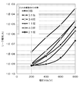
- FIG. 16 is a rewrite of FIG. 15 with respect to the relationship between the number of V pits on the surface of the buffer layer structure and the longitudinal leakage current. 15 and 16 that the leakage current increases as the number of V pits in the buffer structure increases. Therefore, in order to improve the vertical leakage current characteristics, it is necessary to suppress the V pit of the buffer layer structure.
- the present inventors have conducted intensive studies on an epitaxial substrate for electronic devices that can suppress the V pits of the buffer layer structure and improve the longitudinal leakage current characteristics when the electronic device is fabricated. If the surface roughness Sa on the buffer layer side is 4 nm or more, V pits of the buffer layer structure formed on the AlN initial layer are suppressed, and the vertical leakage current characteristics when an electronic device is fabricated is improved. As a result, the present inventors have found that it is possible to achieve the present invention.
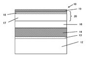
- the electronic device epitaxial substrate 10 of the present invention shown in FIG. 1 has a Si-based substrate 12, an AlN initial layer 13 provided on the Si-based substrate 12, and a buffer layer 14 provided on the AlN initial layer 13.
- the surface roughness Sa on the buffer layer 14 side of the AlN initial layer 13 is 4 nm or more.
- the roughness Sa is defined as a three-dimensional representation of the two-dimensional arithmetic average roughness Ra.
- the Si substrate is a Si substrate or a SiC substrate.
- the high resistance layer 16 can be, for example, a GaN layer containing C or Fe
- the channel layer 17 can be, for example, a GaN layer in which either C or Fe is less than the high resistance layer 16.
- the barrier layer 18 can be, for example, an AlGaN layer
- the cap layer 19 can be, for example, a GaN layer.
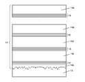
- the detailed configuration of the buffer layer 14 is shown in FIG. 2, and the detailed configuration including the AlN initial layer 13 and the surface roughness Sa of the buffer layer 14 is shown in FIG.
- the buffer layer 14 includes a first layer (Al z Ga 1-z N layer) 14a made of Al z Ga 1-z N (0 ⁇ z ⁇ 1) and a first multilayer film (multilayer film) 15 ′. It can be laminated.
- the first multilayer film 15 ′ is formed by alternately laminating Al x Ga 1-x N (0 ⁇ x ⁇ 1) layers 14b and Al y Ga 1-y N (0 ⁇ y ⁇ x) layers 14c. And a plurality of pairs can be alternately stacked. Further, as shown in FIG.
- a plurality of pairs or a single pair of insertion layers 14d and a second multilayer film 15 are alternately stacked on the first multilayer film 15 ′ (in FIG. 2, a plurality of pairs are stacked). May be a singular pair).
- the insertion layer 14d can be an Al ⁇ Ga 1- ⁇ N (0 ⁇ ⁇ ⁇ 1) layer
- the second multilayer film 15 can be an Al x Ga 1-x N (0 ⁇ x ⁇ 1) layer 14b.
- the Al y Ga 1-y N (0 ⁇ y ⁇ x) layers 14c may be alternately stacked.
- the roughness Sa on the surface of the AlN initial layer 13 on the buffer layer 14 side is set to 4 nm or more, so that V pits of the structure of the buffer layer 14 formed on the AlN initial layer 13 are formed. It is possible to suppress the vertical leakage current characteristics when the electronic device is manufactured.
- the surface roughness Sa of the AlN initial layer 13 is preferably 8 nm or less.
- the roughness Sa on the buffer layer 14 side of the AlN initial layer 13 is 4 nm or more and 8 nm or less, the V pits of the structure of the buffer layer 14 formed on the AlN initial layer 13 are surely suppressed. be able to.
- the roughness of the surface opposite to the AlN initial layer 13 of the first layer 14 a made of Al z Ga 1-z N (0 ⁇ z ⁇ 1) in contact with the AlN initial layer 13. Sa is preferably 0.6 nm or less.
- the roughness Sa of the surface of the first layer 14a opposite to the AlN initial layer 13 is 0.6 nm or less, the longitudinal leakage current characteristics when the electronic device is manufactured can be effectively improved. Can do.
- the roughness Sa of the surface opposite to the AlN initial layer 13 of the first multilayer film 15 ′ in contact with the first layer 14a is 0.3 nm or less.
- the longitudinal leakage current characteristic when the electronic device is manufactured is more effectively obtained. Can be improved.
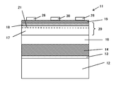
- FIG. 4 includes a source electrode 26, a drain electrode 28, and a gate electrode 30 on the cap layer 19 on the active layer 20 including the channel layer 17 and the barrier layer 18 of the epitaxial substrate 10 for the electronic device of FIG. It is provided.
- the source electrode 26 and the drain electrode 28 are arranged so that current flows from the source electrode 26 to the drain electrode 28 through the two-dimensional electron gas layer 21 formed in the channel layer 17. .
- the current flowing between the source electrode 26 and the drain electrode 28 can be controlled by the potential applied to the gate electrode 30.
- the source electrode 26 and the drain electrode 28 are only required to be connected to the two-dimensional electron gas layer 21 with a low resistance, and are arranged in a region where the cap layer 19 is removed or in a region where the cap layer 19 and the barrier layer 18 are removed. May be. With such an electronic device, it is possible to suppress the V pits of the buffer layer structure formed on the AlN initial layer and improve the vertical leakage current characteristics.
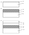
- an AlN initial layer 13 having a thickness of 20 to 200 nm is formed on a Si-based substrate 12 having a thickness of about 1 mm by, for example, MOVPE (organic metal vapor phase epitaxy). Epitaxially grow.
- MOVPE organic metal vapor phase epitaxy
- the surface roughness Sa of the AlN initial layer 13 is 4 nm or more, preferably 4 nm or more and 8 nm or less.
- the surface roughness can be adjusted by changing the growth temperature, the gas flow rate, and the group III element / group V element ratio.
- the buffer layer 14 is epitaxially grown on the AlN initial layer 13 by, for example, the MOVPE method.
- a first layer 14a made of Al z Ga 1-z N having a thickness of about 100 to 500 nm and an Al x Ga 1-x N layer having a thickness of about 3 to 7 nm.
- An insertion layer 14d made of Al ⁇ Ga 1- ⁇ N having a thickness of about 500 nm, an Al x Ga 1-x N layer 14b having a thickness of about 3 to 7 nm, and an Al y Ga 1-y N layer 14c having a thickness of about 2 to 5 nm.
- the first multilayer film 15 alternately stacked with each other to form the buffer layer 14.
- the first layer 14 a is formed to be thicker than each layer constituting the first multilayer film 15 ′ and the second multilayer film 15.
- the surface roughness Sa of the AlN initial layer 13 on the buffer layer 14 side is increased as described above, the lateral growth of the first layer 14a formed on the AlN initial layer 13 is promoted.
- the filling of the surface of the AlN initial layer 13 by the first layer 14a is promoted, and as a result, the surface after the growth of the first layer 14a becomes flat (see FIG. 3), and the first layer 14a on the first layer 14a becomes flat.
- the flatness of one multilayer film 15 ′ can also be improved (see FIG. 3), and the longitudinal leakage current characteristics when an electronic device is manufactured can be improved.
- the high resistance layer 16 for example, a GaN layer containing C or Fe
- the channel layer 17 for example, a GaN layer having less C or Fe than the high resistance layer 16.
- the epitaxial layer 10 for an electronic device shown in FIG. 1 can be manufactured by epitaxially growing a barrier layer 18 such as an AlGaN layer and a cap layer 19 such as a GaN layer thereon by MOVPE, for example.
- MOVPE MOVPE
- V pits in the buffer layer structure formed on the AlN initial layer are suppressed, and the vertical leakage current characteristics when the electronic device is manufactured are improved.
- An epitaxial substrate for an electronic device can be manufactured.
- the epitaxial substrate 10 for the electronic device of FIG. 1 is manufactured, and the source is formed on the cap layer 19 on the active layer 20 including the channel layer 17 and the barrier layer 18 of the epitaxial substrate 10 for the electronic device.
- An electrode 26, a drain electrode 28, and a gate electrode 30 are formed.
- the source electrode 26 and the drain electrode 28 can be formed of, for example, a laminated film of Ti / Al
- the gate electrode 30 can be formed of, for example, a lower layer film made of a metal oxide such as SiO or SiN, and Ni, Au, Mo, Pt. It can be formed of a laminated film of an upper film made of a metal such as.
- the electronic device 11 shown in FIG. 4 is obtained.
- the electronic device manufacturing method as described above it is possible to manufacture an electronic device in which the V pit of the buffer layer structure formed on the AlN initial layer is suppressed and the vertical leakage current characteristics are improved.
- the epitaxial substrate 10 for electronic devices as shown in FIG. 1 was manufactured by changing the roughness of the AlN initial layer surface in the range of 2 nm to 7.5 nm (preparation of 6 levels).
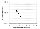
- FIG. 6 shows the relationship between the V pit density (location / cm 2 ) of the buffer layer structure and the roughness Sa of the AlN initial layer surface.
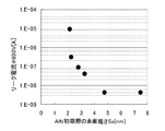
- FIG. 7 shows the relationship between the vertical leakage current and the roughness Sa of the AlN initial layer surface.
- the roughness of the surface of the AlN initial layer is 4 nm or more, there are no V pits (at 4 nm or more, there are almost no V pits and there is no plot on FIG. 6).
- the roughness of the upper surface is 4 nm or more, the vertical leakage current is also improved.
- An AlN initial layer 13 was grown to a thickness of 160 nm on a silicon substrate having a thickness of about 1 mm by the MOVPE method.
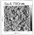
- the AlN initial layer was formed at a growth temperature of 1100 ° C. to 1200 ° C., for example, 1130 ° C., and the surface roughness Sa of the AlN initial layer 13 was 4.79 nm.
- the buffer layer 14 was grown.
- the buffer layer 14 is formed by laminating a first layer 14a made of GaN having a thickness of 300 nm and a first multilayer film 15 ′. Further, an insertion layer 14d made of GaN having a thickness of 300 nm is further formed on the first multilayer film 15 ′.
- the second multilayer film 15 were alternately laminated.
- the first multilayer film 15 ′ and the second multilayer film 15 are formed by alternately stacking AlN layers 14b having a thickness of 5 nm and GaN layers 14c having a thickness of 3 nm.
- a high carbon concentration layer (high resistance layer 16) made of GaN and then a low carbon concentration layer (channel layer 17) also made of GaN were grown.
- a barrier layer 18 made of AlGaN and a GaN layer (cap layer 19) were grown on the barrier layer 18, whereby the epitaxial substrate 10 for electronic devices of FIG. 1 was manufactured.
- FIG. 8 shows a photograph of the surface of the AlN initial layer 13.
- FIG. 3 shows a cross section of the buffer layer 14 after epitaxial growth.
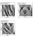
- FIG. 9 shows a photograph of the surface of the first layer 14a.
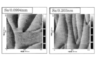
- the roughness Sa of the surface of the first layer 14a was 0.6 nm or less.
- FIG. 10 shows a photograph of the surface of the first multilayer film 15 ′.
- the roughness Sa of the surface of the first multilayer film 15 ′ was 0.3 nm or less. Note that the two photographs in FIG. 10 are photographs of two different wafers.
- Electrodes are formed on this epitaxial substrate for electronic devices, and the electronic device 11 shown in FIG. 4 is manufactured.
- a longitudinal (thickness direction) leakage current is measured by applying a voltage of 600 V, 4 ⁇ 10 ⁇ 9 (A)
- the longitudinal leakage current can be greatly suppressed as compared with the comparative example described later.
- the electronic device epitaxial substrate 10 was manufactured in the same manner as in the example. However, the AlN initial layer 13 was formed at a growth temperature of 1240 ° C., the surface roughness Sa of the AlN initial layer was 2.16 nm, and the others were the same as in the example.
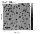
- FIG. 11 shows a photograph of the surface of the AlN initial layer 13.
- FIG. 12 shows a cross section of the AlN initial layer 13 and the buffer layer 14 after epitaxial growth. Thus, it can be seen that the surface of the AlN initial layer 13 is flat, but the surface of the first layer 14a and the surface of the first multilayer film 15 ′ thereon are uneven.
- An electrode was formed on this semiconductor epitaxial wafer, and the electronic device 11 shown in FIG. 4 was manufactured. When a longitudinal leakage current was measured by applying a voltage of 600 V, it was 8.6 ⁇ 10 ⁇ 6 (A).
- the present invention is not limited to the above embodiment.
- the above-described embodiment is an exemplification, and the present invention has substantially the same configuration as the technical idea described in the claims of the present invention, and any device that exhibits the same function and effect is the present invention. It is included in the technical scope of the invention.
- the first multilayer film 15 ′ and the second multilayer film 15 may be a single layer having an Al composition gradient. Further, the second multilayer film 15 or the insertion layer 14 may not be provided.
Landscapes
- Chemical & Material Sciences (AREA)
- Crystallography & Structural Chemistry (AREA)
- Engineering & Computer Science (AREA)
- Materials Engineering (AREA)
- Metallurgy (AREA)
- Organic Chemistry (AREA)
- Chemical Kinetics & Catalysis (AREA)
- General Chemical & Material Sciences (AREA)
- Inorganic Chemistry (AREA)
- Insulated Gate Type Field-Effect Transistor (AREA)
- Junction Field-Effect Transistors (AREA)
- Recrystallisation Techniques (AREA)
Abstract
Description
このような検討において、半導体エピタキシャルウェーハ製造後は、半導体エピタキシャルウェーハ表面にデバイスを作製し、電気特性評価を行っている。
例えば、特許文献1は初期層のAlN層の粗さに触れるものであり、AlN層に接するシリコン基板の表面粗さRaを0.2~1nmとすることで、その上方に成長するIII族窒化物半導体の結晶性を向上させることを開示している。しかしながら、特許文献1には電気特性に関しての言及はない。
しかしながら、バッファ層構造のVピットをどのようにして抑制するかについては、検討の余地があった。
このようにAlN初期層のバッファ層側の表面の粗さSaが8nm以下であれば、AlN初期層の上に形成されるバッファ層構造のVピットを確実に抑制することができる。
このようにAlzGa1-zN層のAlN初期層と反対側の表面の粗さSaが0.6nm以下であれば、電子デバイスを作製したときの縦方向リーク電流特性を効果的に改善することができる。
このように多層膜のAlzGa1-zN(0≦z<1)層と反対側の表面の粗さSaが0.3nm以下であれば、電子デバイスを作製したときの縦方向リーク電流特性をより効果的に改善することができる。
このような構成であれば、電子デバイス用エピタキシャル基板として、好適に用いることができる。
前述のように、本発明者らは、Si基板上にGaN膜をエピタキシャル成長させたエピタキシャルウェーハの電気的特性について検討を行った。その検討において、縦方向リーク電流特性の悪いものから、良いものまでを任意に選び、それぞれのウェーハを2分割し、一方の2分割ウェーハで縦方向リーク電流特性評価を行い、他方の2分割ウェーハで故障解析(断面観察)を行った。
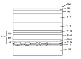
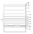
ここで、バッファ層構造のVピットについて説明する。本来、バッファ層の各層は、基板に対して平行に積層されなければならない。「Vピット」とは、基板に対して平行ではなく一部に窪みができて、多層膜やAlzGa1-zN(0≦z<1)挿入層が平らになっていない部分(図13の楕円で囲んだ部分)をいう。
各ウェーハについて、隣り合わない任意の5点(すなわち、少し離した5箇所)を観察して、バッファ層構造のVピットの数を数えた(図13、図14参照)。
ここで、図13はバッファ層構造のVピットを説明するための断面図であり、図14はバッファ層構造のVピットが生じている電子デバイス用エピタキシャル基板を示す断面図である。また、図13、図14において、電子デバイス用エピタキシャル基板100は、Si基板112と、Si基板112上に設けられたAlN初期層113と、AlN初期層113上に設けられたバッファ層114を有している。バッファ層114は、AlzGa1-zNからなる第1の層114aと、第1の多層膜115’とが積層され、第1の多層膜115’上にさらに、AlαGa1-αN(0≦α<1)挿入層114dと、第2の多層膜115とが交互に積層されることにより形成されている。電子デバイス用エピタキシャル基板100は、バッファ層114上に設けられた高抵抗層116と、高抵抗層116上に設けられたチャネル層117と、チャネル層117上に設けられたバリア層118と、バリア層118上に設けられたキャップ層119をさらに有している。
図15、図16からバッファ構造のVピットの数が増加するに従いリーク電流が増加することがわかる。
従って、縦方向リーク電流特性を改善するには、バッファ層構造のVピットを抑制する必要がある。
図1に示す本発明の電子デバイス用エピタキシャル基板10は、Si系基板12と、Si系基板12上に設けられたAlN初期層13と、AlN初期層13上に設けられたバッファ層14を有しており、AlN初期層13のバッファ層14側の表面の粗さSaは4nm以上である。ここで、粗さSaは2次元の算術的平均粗さRaを3次元化したものとして定義されるものである。また、Si系基板とは、Si基板又はSiC基板である。
図1の電子デバイス用エピタキシャル基板10は、バッファ層14上に設けられた高抵抗層16と、高抵抗層16上に設けられたチャネル層17と、チャネル層17上に設けられたバリア層18と、バリア層18上に設けられたキャップ層19をさらに有することができる。ここで、チャネル層17とバリア層18は、能動層20を形成している。
高抵抗層16は、例えば、C又はFeを含むGaN層とすることができ、チャネル層17は、例えば、C又はFeのいずれかが高抵抗層16よりも少ないGaN層とすることができ、バリア層18は、例えば、AlGaN層とすることができ、キャップ層19は、例えば、GaN層とすることができる。
挿入層14dは、AlαGa1-αN(0≦α<1)層とすることができ、第2の多層膜15はAlxGa1-xN(0<x≦1)層14bとAlyGa1-yN(0≦y<x)層14cとが交互に積層されたものとすることができる。
このようにAlN初期層13のバッファ層14側の表面の粗さSaが4nm以上8nm以下であれば、AlN初期層13の上に形成されるバッファ層14の構造のVピットを確実に抑制することができる。
このように第1の層14aのAlN初期層13と反対側の表面の粗さSaが0.6nm以下であれば、電子デバイスを作製したときの縦方向リーク電流特性を効果的に改善することができる。
このように第1多層膜15’の第1の層14aと反対側の表面の粗さSaが0.3nm以下であれば、電子デバイスを作製したときの縦方向リーク電流特性をより効果的に改善することができる。
図4の電子デバイス11は、図1の電子デバイス用エピタキシャル基板10のチャネル層17とバリア層18からなる能動層20上のキャップ層19上に、ソース電極26、ドレイン電極28、ゲート電極30を設けたものである。電子デバイス11において、ソース電極26及びドレイン電極28は、ソース電極26から、チャネル層17内に形成された二次元電子ガス層21を介して、ドレイン電極28に電流が流れるように配置されている。ソース電極26とドレイン電極28との間に流れる電流は、ゲート電極30に印加される電位によってコントロールすることができる。なお、ソース電極26、ドレイン電極28は二次元電子ガス層21と低抵抗接続されていればよく、キャップ層19を除去した領域、又は、キャップ層19及びバリア層18を除去した領域に配置してもよい。
このような電子デバイスであれば、AlN初期層の上に形成されるバッファ層構造のVピットを抑制し、縦方向リーク電流特性を改善することができる。
まず、図5(a)に示すように、厚さ1mm程度のSi系基板12上に、例えば、MOVPE法(有機金属気相成長法)により、AlN初期層13を20~200nmの厚さでエピタキシャル成長させる。
ここでAlN初期層13の表面の粗さSaを4nm以上、好ましくは4nm以上8nm以下にする。なお、AlN初期層13の表面を粗くするには、成長温度、ガス流量、III族元素/V族元素比を変更することで表面の粗さを調整することができる。
具体的には、図2に示すように、厚さ100~500nm程度のAlzGa1-zNからなる第1の層14aと、厚さ3~7nm程度のAlxGa1-xN層14bと厚さ2~5nm程度のAlyGa1-yN層14cとが交互に積層された第1多層膜15’とを積層し、第1多層膜15’上にさらに、厚さ100~500nm程度のAlαGa1-αNからなる挿入層14dと、厚さ3~7nm程度のAlxGa1-xN層14bと厚さ2~5nm程度のAlyGa1-yN層14cとが交互に積層された第1多層膜15と、を交互に積層して、バッファ層14を形成する。ここで、第1の層14aは、第1多層膜15’、第2多層膜15を構成する各層よりも厚く形成する。
このとき、AlN初期層13のバッファ層14側の表面の粗さSaを上記のように大きくしているので、AlN初期層13上に形成される第1の層14aの横方向成長が促進され、第1の層14aによるAlN初期層13の表面の穴埋めが促進され、その結果、第1の層14a成長後の表面が平坦になり(図3を参照)、第1の層14a上の第1多層膜15’の平坦性も向上させることができ(図3を参照)、電子デバイスを作製したときの縦方向リーク電流特性を改善することができる。
上記のような電子デバイス用エピタキシャル基板の製造方法であれば、AlN初期層の上に形成されるバッファ層構造のVピットが抑制され、電子デバイスを作製したときの縦方向リーク電流特性が改善される電子デバイス用エピタキシャル基板を製造することができる。
上記で説明したように、図1の電子デバイス用エピタキシャル基板10を製造し、さらに、電子デバイス用エピタキシャル基板10のチャネル層17とバリア層18からなる能動層20上のキャップ層19上に、ソース電極26、ドレイン電極28、ゲート電極30を形成する。ソース電極26及びドレイン電極28は例えば、Ti/Alの積層膜で形成することができ、ゲート電極30は例えば、SiO、SiN等の金属酸化物からなる下層膜と、Ni、Au、Mo、Pt等の金属からなる上層膜の積層膜で形成することができる。このようにして、図4に示す電子デバイス11が得られる。
上記のような電子デバイスの製造方法であれば、AlN初期層の上に形成されるバッファ層構造のVピットが抑制され、縦方向リーク電流特性が改善される電子デバイスを製造することができる。
AlN初期層表面の粗さを2nm~7.5nmの範囲で変えて(6水準作成)、図1に示すような電子デバイス用エピタキシャル基板10を製造した。バッファ層構造のVピット密度(箇所/cm2)とAlN初期層表面の粗さSaとの関係を図6に示す。また、縦方向リーク電流とAlN初期層表面の粗さSaとの関係を図7に示す。図6からわかるようにAlN初期層表面の粗さが4nm以上でVピットは無くなり(4nm以上ではVピットはほとんどなくなり、図6上にはプロットがない)、図7からわかるようにAlN初期層上面の粗さが4nm以上で縦方向リーク電流も改善されている。
厚さ1mm程度のシリコン基板上にMOVPE法によりAlN初期層13を160nmの厚さで成長させた。ここで、AlN初期層を成長温度1100℃~1200℃、例えば、1130℃で形成し、AlN初期層13の表面の粗さSaを4.79nmとした。
次にバッファ層14を成長させた。バッファ層14は厚さ300nmのGaNからなる第1の層14aと、第1多層膜15’とを積層させ、第一多層膜15’上にさらに、厚さ300nmのGaNからなる挿入層14dと、第2多層膜15とを交互に積層させた。第1多層膜15’、第2多層膜15は、厚さ5nmのAlN層14bと厚さ3nmのGaN層14cとを交互に積層した。
次にGaNからなる高炭素濃度層(高抵抗層16)、続いて、同じくGaNからなる低炭素濃度層(チャネル層17)を成長させた。続いて、AlGaNからなるバリア層18、その上にGaN層(キャップ層19)を成長させることで、図1の電子デバイス用エピタキシャル基板10を製造した。
図9に第1の層14a表面の写真を示す。第1の層14a表面の粗さSaは、0.6nm以下になっていた。なお、図9の3つの写真は、異なる3枚のウェーハの写真である。
図10に第1多層膜15’表面の写真を示す。第1多層膜15’表面の粗さSaは、0.3nm以下になっていた。なお、図10の2つの写真は、異なる2枚のウェーハの写真である。
この電子デバイス用エピタキシャル基板に電極を形成し、図4に示す電子デバイス11を製造し、600Vの電圧をかけて縦方向(厚み方向)リーク電流を測定したところ、4×10⁻⁹(A)となり、後述する比較例に比べて大幅に縦方向リーク電流を抑制することができた。
実施例と同様にして、電子デバイス用エピタキシャル基板10を製造した。ただし、AlN初期層13を成長温度1240℃で形成し、AlN初期層の表面の粗さSaを2.16nmとし、その他は実施例と同じとした。
図11にAlN初期層13表面の写真を示す。また、図12にエピタキシャル成長後のAlN初期層13及びバッファ層14の断面を示す。このようにAlN初期層13の表面は平らであるが、その上の第1の層14a表面、及び、第1多層膜15’表面は凸凹形状になっているのがわかる。この半導体エピタキシャルウェーハに電極を形成し、図4に示す電子デバイス11を製造し、600Vの電圧をかけて縦方向リーク電流を測定したところ、8.6×10⁻⁶(A)となった。
Claims (8)
- Si系基板と、該Si系基板上に設けられたAlN初期層と、該AlN初期層上に設けられたバッファ層とを有する電子デバイス用エピタキシャル基板であって、
前記AlN初期層の前記バッファ層側の表面の粗さSaが4nm以上であることを特徴とする電子デバイス用エピタキシャル基板。 - 前記AlN初期層表面の前記バッファ層側の粗さSaが8nm以下であることを特徴とする請求項1に記載の電子デバイス用エピタキシャル基板。
- 前記バッファ層は、前記AlN初期層に接しているAlzGa1-zN(0≦z<1)層を含み、
前記AlzGa1-zN(0≦z<1)層の前記AlN初期層と反対側の表面の粗さSaが0.6nm以下であることを特徴とする請求項1又は請求項2に記載の電子デバイス用エピタキシャル基板。 - 前記バッファ層は、前記AlzGa1-zN(0≦z<1)層に接し、かつ、AlxGa1-xN(0<x≦1)層とAlyGa1-yN(0≦y<x)層とが交互に積層された多層膜を含み、
前記多層膜の前記AlzGa1-zN(0≦z<1)層と反対側の表面の粗さSaが0.3nm以下であることを特徴とする請求項3に記載の電子デバイス用エピタキシャル基板。 - 前記バッファ層上に設けられたチャネル層と、
該チャネル層上に設けられたバリア層と、
該バリア層上に設けられたキャップ層と
をさらに有することを特徴とする請求項1から請求項4のいずれか一項に記載の電子デバイス用エピタキシャル基板。 - 請求項1から請求項5のいずれか一項に記載の電子デバイス用エピタキシャル基板を用いて作製された電子デバイスであって、前記電子デバイス用エピタキシャル基板上に電極が設けられているものであることを特徴とする電子デバイス。
- Si系基板上にAlN初期層を形成する工程と、
前記AlN初期層上にバッファ層を形成する工程と、
前記バッファ層上にチャネル層を形成する工程と、
前記チャネル層上にバリア層を形成する工程と、
前記バリア層上にキャップ層を形成する工程と
を有し、
前記AlN初期層の前記バッファ層側の表面の粗さSaを4nm以上とすることを特徴とする電子デバイス用エピタキシャル基板の製造方法。 - Si系基板上にAlN初期層を形成する工程と、
前記AlN初期層上にバッファ層を形成する工程と、
前記バッファ層上にチャネル層を形成する工程と、
前記チャネル層上にバリア層を形成する工程と、
前記バリア層上にキャップ層を形成する工程と、
前記キャップ層上に電極を形成する工程と
を有し、
前記AlN初期層の前記バッファ層側の表面の粗さSaを4nm以上とすることを特徴とする電子デバイスの製造方法。
Priority Applications (3)
| Application Number | Priority Date | Filing Date | Title |
|---|---|---|---|
| US15/538,500 US10115589B2 (en) | 2015-01-08 | 2015-12-18 | Epitaxial substrate for electronic devices, electronic device, method for producing the epitaxial substrate for electronic devices, and method for producing the electronic device |
| KR1020177018664A KR20170101932A (ko) | 2015-01-08 | 2015-12-18 | 전자 디바이스용 에피택셜 기판, 전자 디바이스, 전자 디바이스용 에피택셜 기판의 제조 방법, 그리고 전자 디바이스의 제조 방법 |
| CN201580072647.8A CN107112242B (zh) | 2015-01-08 | 2015-12-18 | 电子器件用外延基板、电子器件、电子器件用外延基板的制造方法及电子器件的制造方法 |
Applications Claiming Priority (2)
| Application Number | Priority Date | Filing Date | Title |
|---|---|---|---|
| JP2015002047A JP6261523B2 (ja) | 2015-01-08 | 2015-01-08 | 電子デバイス用エピタキシャル基板の製造方法、並びに電子デバイスの製造方法 |
| JP2015-002047 | 2015-01-08 |
Publications (1)
| Publication Number | Publication Date |
|---|---|
| WO2016110906A1 true WO2016110906A1 (ja) | 2016-07-14 |
Family
ID=56355636
Family Applications (1)
| Application Number | Title | Priority Date | Filing Date |
|---|---|---|---|
| PCT/JP2015/006313 Ceased WO2016110906A1 (ja) | 2015-01-08 | 2015-12-18 | 電子デバイス用エピタキシャル基板、電子デバイス、電子デバイス用エピタキシャル基板の製造方法、並びに電子デバイスの製造方法 |
Country Status (6)
| Country | Link |
|---|---|
| US (1) | US10115589B2 (ja) |
| JP (1) | JP6261523B2 (ja) |
| KR (1) | KR20170101932A (ja) |
| CN (1) | CN107112242B (ja) |
| TW (1) | TWI624879B (ja) |
| WO (1) | WO2016110906A1 (ja) |
Cited By (1)
| Publication number | Priority date | Publication date | Assignee | Title |
|---|---|---|---|---|
| US12119398B2 (en) | 2017-11-20 | 2024-10-15 | Rohm Co., Ltd. | Semiconductor device |
Families Citing this family (6)
| Publication number | Priority date | Publication date | Assignee | Title |
|---|---|---|---|---|
| JP6239017B2 (ja) * | 2015-03-31 | 2017-11-29 | クアーズテック株式会社 | 窒化物半導体基板 |
| US10388518B2 (en) | 2017-03-31 | 2019-08-20 | Globalwafers Co., Ltd. | Epitaxial substrate and method of manufacturing the same |
| JP2019125737A (ja) * | 2018-01-18 | 2019-07-25 | 株式会社サイオクス | 窒化物半導体エピタキシャル基板 |
| US11515408B2 (en) | 2020-03-02 | 2022-11-29 | Taiwan Semiconductor Manufacturing Company, Ltd. | Rough buffer layer for group III-V devices on silicon |
| US20220122838A1 (en) * | 2020-10-21 | 2022-04-21 | University Of South Carolina | Approaches for Fabricating N-Polar AlxGa1-xN Templates for Electronic and Optoelectronic Devices |
| US20230031662A1 (en) * | 2021-04-02 | 2023-02-02 | Innoscience (Suzhou) Technology Co., Ltd. | Iii nitride semiconductor wafers |
Citations (3)
| Publication number | Priority date | Publication date | Assignee | Title |
|---|---|---|---|---|
| WO2011016304A1 (ja) * | 2009-08-07 | 2011-02-10 | 日本碍子株式会社 | 半導体素子用エピタキシャル基板、半導体素子用エピタキシャル基板の製造方法、および半導体素子 |
| JP2011114267A (ja) * | 2009-11-30 | 2011-06-09 | Sanken Electric Co Ltd | 半導体装置 |
| JP2013042032A (ja) * | 2011-08-18 | 2013-02-28 | Fujitsu Ltd | 化合物半導体装置及びその製造方法 |
Family Cites Families (12)
| Publication number | Priority date | Publication date | Assignee | Title |
|---|---|---|---|---|
| JP2008078613A (ja) * | 2006-08-24 | 2008-04-03 | Rohm Co Ltd | 窒化物半導体の製造方法及び窒化物半導体素子 |
| JP4677499B2 (ja) * | 2008-12-15 | 2011-04-27 | Dowaエレクトロニクス株式会社 | 電子デバイス用エピタキシャル基板およびその製造方法 |
| JP2011023677A (ja) * | 2009-07-21 | 2011-02-03 | Hitachi Cable Ltd | 化合物半導体エピタキシャルウェハおよびその製造方法 |
| JP5378128B2 (ja) | 2009-09-18 | 2013-12-25 | Dowaエレクトロニクス株式会社 | 電子デバイス用エピタキシャル基板およびiii族窒化物電子デバイス用エピタキシャル基板 |
| US9006865B2 (en) * | 2010-06-25 | 2015-04-14 | Dowa Electronics Materials Co., Ltd. | Epitaxial growth substrate, semiconductor device, and epitaxial growth method |
| KR101820327B1 (ko) * | 2010-08-07 | 2018-01-19 | 티피케이 홀딩 컴퍼니 리미티드 | 표면 매립 첨가제를 가진 디바이스 콤포넌트 및 이와 관련된 제조 방법 |
| JP6035721B2 (ja) * | 2011-09-27 | 2016-11-30 | 住友電気工業株式会社 | 半導体装置の製造方法 |
| JP6130995B2 (ja) * | 2012-02-20 | 2017-05-17 | サンケン電気株式会社 | エピタキシャル基板及び半導体装置 |
| JP6152700B2 (ja) * | 2013-05-23 | 2017-06-28 | 住友電気工業株式会社 | 半導体装置の製造方法 |
| TWI523222B (zh) * | 2013-10-14 | 2016-02-21 | 國立交通大學 | 含氮化鎵之半導體結構 |
| KR102145205B1 (ko) * | 2014-04-25 | 2020-08-19 | 삼성전자주식회사 | 반도체 소자 제조방법 및 증착 장치의 유지보수방법 |
| US9337023B1 (en) * | 2014-12-15 | 2016-05-10 | Texas Instruments Incorporated | Buffer stack for group IIIA-N devices |
-
2015
- 2015-01-08 JP JP2015002047A patent/JP6261523B2/ja active Active
- 2015-12-18 CN CN201580072647.8A patent/CN107112242B/zh active Active
- 2015-12-18 US US15/538,500 patent/US10115589B2/en active Active
- 2015-12-18 WO PCT/JP2015/006313 patent/WO2016110906A1/ja not_active Ceased
- 2015-12-18 KR KR1020177018664A patent/KR20170101932A/ko not_active Ceased
- 2015-12-28 TW TW104144060A patent/TWI624879B/zh active
Patent Citations (3)
| Publication number | Priority date | Publication date | Assignee | Title |
|---|---|---|---|---|
| WO2011016304A1 (ja) * | 2009-08-07 | 2011-02-10 | 日本碍子株式会社 | 半導体素子用エピタキシャル基板、半導体素子用エピタキシャル基板の製造方法、および半導体素子 |
| JP2011114267A (ja) * | 2009-11-30 | 2011-06-09 | Sanken Electric Co Ltd | 半導体装置 |
| JP2013042032A (ja) * | 2011-08-18 | 2013-02-28 | Fujitsu Ltd | 化合物半導体装置及びその製造方法 |
Non-Patent Citations (1)
| Title |
|---|
| A. ABLE ET AL.: "Growth of crack-free GaN on Si(1 1 1) with graded AlGaN buffer layers", JOURNAL OF CRYSTAL GROWTH, vol. 276, no. 3-4, pages 415 - 418, XP004806888, DOI: doi:10.1016/j.jcrysgro.2004.12.003 * |
Cited By (1)
| Publication number | Priority date | Publication date | Assignee | Title |
|---|---|---|---|---|
| US12119398B2 (en) | 2017-11-20 | 2024-10-15 | Rohm Co., Ltd. | Semiconductor device |
Also Published As
| Publication number | Publication date |
|---|---|
| JP6261523B2 (ja) | 2018-01-17 |
| CN107112242A (zh) | 2017-08-29 |
| JP2016127223A (ja) | 2016-07-11 |
| TWI624879B (zh) | 2018-05-21 |
| US20170352537A1 (en) | 2017-12-07 |
| CN107112242B (zh) | 2020-11-13 |
| US10115589B2 (en) | 2018-10-30 |
| KR20170101932A (ko) | 2017-09-06 |
| TW201635394A (zh) | 2016-10-01 |
Similar Documents
| Publication | Publication Date | Title |
|---|---|---|
| JP6261523B2 (ja) | 電子デバイス用エピタキシャル基板の製造方法、並びに電子デバイスの製造方法 | |
| JP6473017B2 (ja) | 化合物半導体基板 | |
| JP6170893B2 (ja) | 半導体素子用エピタキシャル基板の作製方法 | |
| JP2022136128A (ja) | 半導体装置及びその製造方法 | |
| JP5252813B2 (ja) | 半導体装置の製造方法 | |
| JP5665171B2 (ja) | Iii族窒化物半導体電子デバイス、iii族窒化物半導体電子デバイスを作製する方法 | |
| JP3960957B2 (ja) | 半導体電子デバイス | |
| KR102211209B1 (ko) | 질화알루미늄 기반 트랜지스터의 제조 방법 | |
| JP4276135B2 (ja) | 窒化物半導体成長用基板 | |
| CN105247658B (zh) | 半导体基板、半导体装置及半导体装置的制造方法 | |
| US8633514B2 (en) | Group III nitride semiconductor wafer and group III nitride semiconductor device | |
| JP5134265B2 (ja) | 半導体装置とその製造方法 | |
| JP6239017B2 (ja) | 窒化物半導体基板 | |
| CN106024588A (zh) | 一种选择区域外延生长界面改善方法 | |
| JP4933513B2 (ja) | 窒化物半導体成長用基板 | |
| JP6029538B2 (ja) | 半導体装置 | |
| JP2009231302A (ja) | 窒化物半導体結晶薄膜およびその作製方法、半導体装置およびその製造方法 | |
| JP2016157801A (ja) | 半導体装置およびその製造方法 | |
| JP6174253B2 (ja) | 窒化物系化合物半導体 | |
| JP2012064977A (ja) | Iii族窒化物半導体積層ウェハ及びiii族窒化物半導体デバイス | |
| CN103348479A (zh) | 半导体器件 | |
| JP2016157875A (ja) | 半導体積層構造体及びその製造方法、並びに半導体素子及びその製造方法 | |
| JP2016039314A (ja) | 化合物半導体基板 |
Legal Events
| Date | Code | Title | Description |
|---|---|---|---|
| 121 | Ep: the epo has been informed by wipo that ep was designated in this application |
Ref document number: 15876786 Country of ref document: EP Kind code of ref document: A1 |
|
| WWE | Wipo information: entry into national phase |
Ref document number: 15538500 Country of ref document: US |
|
| ENP | Entry into the national phase |
Ref document number: 20177018664 Country of ref document: KR Kind code of ref document: A |
|
| NENP | Non-entry into the national phase |
Ref country code: DE |
|
| 122 | Ep: pct application non-entry in european phase |
Ref document number: 15876786 Country of ref document: EP Kind code of ref document: A1 |