WO2016067748A1 - 電子部品の実装構造 - Google Patents
電子部品の実装構造 Download PDFInfo
- Publication number
- WO2016067748A1 WO2016067748A1 PCT/JP2015/075194 JP2015075194W WO2016067748A1 WO 2016067748 A1 WO2016067748 A1 WO 2016067748A1 JP 2015075194 W JP2015075194 W JP 2015075194W WO 2016067748 A1 WO2016067748 A1 WO 2016067748A1
- Authority
- WO
- WIPO (PCT)
- Prior art keywords
- electronic component
- component package
- metal pattern
- heat dissipation
- pattern
- Prior art date
- Legal status (The legal status is an assumption and is not a legal conclusion. Google has not performed a legal analysis and makes no representation as to the accuracy of the status listed.)
- Ceased
Links
Images


Classifications
-
- H—ELECTRICITY
- H10—SEMICONDUCTOR DEVICES; ELECTRIC SOLID-STATE DEVICES NOT OTHERWISE PROVIDED FOR
- H10W—GENERIC PACKAGES, INTERCONNECTIONS, CONNECTORS OR OTHER CONSTRUCTIONAL DETAILS OF DEVICES COVERED BY CLASS H10
- H10W40/00—Arrangements for thermal protection or thermal control
- H10W40/20—Arrangements for cooling
- H10W40/22—Arrangements for cooling characterised by their shape, e.g. having conical or cylindrical projections
-
- H—ELECTRICITY
- H05—ELECTRIC TECHNIQUES NOT OTHERWISE PROVIDED FOR
- H05K—PRINTED CIRCUITS; CASINGS OR CONSTRUCTIONAL DETAILS OF ELECTRIC APPARATUS; MANUFACTURE OF ASSEMBLAGES OF ELECTRICAL COMPONENTS
- H05K1/00—Printed circuits
- H05K1/02—Details
- H05K1/0201—Thermal arrangements, e.g. for cooling, heating or preventing overheating
- H05K1/0203—Cooling of mounted components
-
- H—ELECTRICITY
- H05—ELECTRIC TECHNIQUES NOT OTHERWISE PROVIDED FOR
- H05K—PRINTED CIRCUITS; CASINGS OR CONSTRUCTIONAL DETAILS OF ELECTRIC APPARATUS; MANUFACTURE OF ASSEMBLAGES OF ELECTRICAL COMPONENTS
- H05K1/00—Printed circuits
- H05K1/18—Printed circuits structurally associated with non-printed electric components
- H05K1/181—Printed circuits structurally associated with non-printed electric components associated with surface mounted components
-
- H—ELECTRICITY
- H05—ELECTRIC TECHNIQUES NOT OTHERWISE PROVIDED FOR
- H05K—PRINTED CIRCUITS; CASINGS OR CONSTRUCTIONAL DETAILS OF ELECTRIC APPARATUS; MANUFACTURE OF ASSEMBLAGES OF ELECTRICAL COMPONENTS
- H05K3/00—Apparatus or processes for manufacturing printed circuits
- H05K3/30—Assembling printed circuits with electric components, e.g. with resistors
- H05K3/32—Assembling printed circuits with electric components, e.g. with resistors electrically connecting electric components or wires to printed circuits
- H05K3/34—Assembling printed circuits with electric components, e.g. with resistors electrically connecting electric components or wires to printed circuits by soldering
- H05K3/3494—Heating processes for reflow soldering
-
- H—ELECTRICITY
- H05—ELECTRIC TECHNIQUES NOT OTHERWISE PROVIDED FOR
- H05K—PRINTED CIRCUITS; CASINGS OR CONSTRUCTIONAL DETAILS OF ELECTRIC APPARATUS; MANUFACTURE OF ASSEMBLAGES OF ELECTRICAL COMPONENTS
- H05K7/00—Constructional details common to different types of electric apparatus
- H05K7/20—Modifications to facilitate cooling, ventilating, or heating
-
- H—ELECTRICITY
- H10—SEMICONDUCTOR DEVICES; ELECTRIC SOLID-STATE DEVICES NOT OTHERWISE PROVIDED FOR
- H10W—GENERIC PACKAGES, INTERCONNECTIONS, CONNECTORS OR OTHER CONSTRUCTIONAL DETAILS OF DEVICES COVERED BY CLASS H10
- H10W40/00—Arrangements for thermal protection or thermal control
- H10W40/20—Arrangements for cooling
- H10W40/22—Arrangements for cooling characterised by their shape, e.g. having conical or cylindrical projections
- H10W40/226—Arrangements for cooling characterised by their shape, e.g. having conical or cylindrical projections characterised by projecting parts, e.g. fins to increase surface area
- H10W40/228—Arrangements for cooling characterised by their shape, e.g. having conical or cylindrical projections characterised by projecting parts, e.g. fins to increase surface area the projecting parts being wire-shaped or pin-shaped
-
- H—ELECTRICITY
- H10—SEMICONDUCTOR DEVICES; ELECTRIC SOLID-STATE DEVICES NOT OTHERWISE PROVIDED FOR
- H10W—GENERIC PACKAGES, INTERCONNECTIONS, CONNECTORS OR OTHER CONSTRUCTIONAL DETAILS OF DEVICES COVERED BY CLASS H10
- H10W70/00—Package substrates; Interposers; Redistribution layers [RDL]
- H10W70/40—Leadframes
- H10W70/421—Shapes or dispositions
-
- H—ELECTRICITY
- H10—SEMICONDUCTOR DEVICES; ELECTRIC SOLID-STATE DEVICES NOT OTHERWISE PROVIDED FOR
- H10W—GENERIC PACKAGES, INTERCONNECTIONS, CONNECTORS OR OTHER CONSTRUCTIONAL DETAILS OF DEVICES COVERED BY CLASS H10
- H10W74/00—Encapsulations, e.g. protective coatings
- H10W74/10—Encapsulations, e.g. protective coatings characterised by their shape or disposition
- H10W74/111—Encapsulations, e.g. protective coatings characterised by their shape or disposition the semiconductor body being completely enclosed
- H10W74/129—Encapsulations, e.g. protective coatings characterised by their shape or disposition the semiconductor body being completely enclosed forming a chip-scale package [CSP]
-
- H—ELECTRICITY
- H10—SEMICONDUCTOR DEVICES; ELECTRIC SOLID-STATE DEVICES NOT OTHERWISE PROVIDED FOR
- H10W—GENERIC PACKAGES, INTERCONNECTIONS, CONNECTORS OR OTHER CONSTRUCTIONAL DETAILS OF DEVICES COVERED BY CLASS H10
- H10W74/00—Encapsulations, e.g. protective coatings
- H10W74/40—Encapsulations, e.g. protective coatings characterised by their materials
- H10W74/47—Encapsulations, e.g. protective coatings characterised by their materials comprising organic materials, e.g. plastics or resins
-
- H—ELECTRICITY
- H05—ELECTRIC TECHNIQUES NOT OTHERWISE PROVIDED FOR
- H05K—PRINTED CIRCUITS; CASINGS OR CONSTRUCTIONAL DETAILS OF ELECTRIC APPARATUS; MANUFACTURE OF ASSEMBLAGES OF ELECTRICAL COMPONENTS
- H05K2201/00—Indexing scheme relating to printed circuits covered by H05K1/00
- H05K2201/10—Details of components or other objects attached to or integrated in a printed circuit board
- H05K2201/10613—Details of electrical connections of non-printed components, e.g. special leads
- H05K2201/10621—Components characterised by their electrical contacts
- H05K2201/10628—Leaded surface mounted device
-
- H—ELECTRICITY
- H05—ELECTRIC TECHNIQUES NOT OTHERWISE PROVIDED FOR
- H05K—PRINTED CIRCUITS; CASINGS OR CONSTRUCTIONAL DETAILS OF ELECTRIC APPARATUS; MANUFACTURE OF ASSEMBLAGES OF ELECTRICAL COMPONENTS
- H05K2201/00—Indexing scheme relating to printed circuits covered by H05K1/00
- H05K2201/20—Details of printed circuits not provided for in H05K2201/01 - H05K2201/10
- H05K2201/2081—Compound repelling a metal, e.g. solder
-
- H—ELECTRICITY
- H10—SEMICONDUCTOR DEVICES; ELECTRIC SOLID-STATE DEVICES NOT OTHERWISE PROVIDED FOR
- H10W—GENERIC PACKAGES, INTERCONNECTIONS, CONNECTORS OR OTHER CONSTRUCTIONAL DETAILS OF DEVICES COVERED BY CLASS H10
- H10W70/00—Package substrates; Interposers; Redistribution layers [RDL]
- H10W70/40—Leadframes
- H10W70/421—Shapes or dispositions
- H10W70/424—Cross-sectional shapes
-
- H—ELECTRICITY
- H10—SEMICONDUCTOR DEVICES; ELECTRIC SOLID-STATE DEVICES NOT OTHERWISE PROVIDED FOR
- H10W—GENERIC PACKAGES, INTERCONNECTIONS, CONNECTORS OR OTHER CONSTRUCTIONAL DETAILS OF DEVICES COVERED BY CLASS H10
- H10W70/00—Package substrates; Interposers; Redistribution layers [RDL]
- H10W70/60—Insulating or insulated package substrates; Interposers; Redistribution layers
- H10W70/67—Insulating or insulated package substrates; Interposers; Redistribution layers characterised by their insulating layers or insulating parts
- H10W70/68—Shapes or dispositions thereof
- H10W70/685—Shapes or dispositions thereof comprising multiple insulating layers
-
- H—ELECTRICITY
- H10—SEMICONDUCTOR DEVICES; ELECTRIC SOLID-STATE DEVICES NOT OTHERWISE PROVIDED FOR
- H10W—GENERIC PACKAGES, INTERCONNECTIONS, CONNECTORS OR OTHER CONSTRUCTIONAL DETAILS OF DEVICES COVERED BY CLASS H10
- H10W74/00—Encapsulations, e.g. protective coatings
Definitions
- This case relates to the mounting structure of electronic parts.
- Such an electronic component is installed in an electronic device in a state of being mounted on an electronic substrate or the like (see, for example, Patent Document 1).
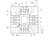
- terminals 2 protruding from (one of) the side portions 1 a to 1 d of the electronic component package 1 are provided on the electronic substrate 3. There are some which are superposed on the provided land 4 and soldered by a reflow method.
- the chip heat radiating member 5 provided on the bottom surface of the electronic component package 1 is superposed on the heat radiating metal pattern 6 provided on the electronic substrate 3 and soldered by a reflow method.
- the electronic component mounting structure has the following problems. That is, for example, when the amount of solder that joins the chip heat radiating member 5 and the heat radiating metal pattern 6 is too large, surplus solder that sticks out from the electronic component package 1 is random from the side portion of the electronic component package 1. Jumps out to become solder balls 13 or the like, and may come into contact with the terminal 2 or the land 4 to cause a short circuit.
- the main purpose of this case is to solve the above-mentioned problems.
- a terminal projecting from a side portion of the electronic component package is soldered by a reflow method over a land provided on an electronic substrate, and a chip heat dissipation member provided on the bottom surface of the electronic component package
- the chip heat dissipation member is formed in a size that is surrounded on all sides by a package resin that constitutes the electronic component package,
- the heat dissipating metal pattern extends so as to protrude from the electronic component package continuously with the heat dissipating metal pattern so that at least a part of the heat dissipating metal pattern is larger than the electronic component package, and guides excess solder to the outside of the electronic component package. It has the pattern extension part integrally.
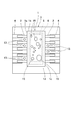
- FIG. 1 It is a top view of the mounting structure of the electronic component concerning this Embodiment. It is a top view of the mounting structure of the electronic component concerning the modification of FIG. It is sectional drawing of the mounting structure of an electronic component which shows the state before installing an electronic component package with respect to an electronic substrate. It is sectional drawing of the mounting structure of the electronic component which shows a state when an electronic component package is installed with respect to the electronic substrate. It is sectional drawing of the mounting structure of the electronic component which shows the state after soldering the electronic component package with respect to the electronic substrate. It is a top view of the heat radiating metal pattern which has a slit part extended in the whole extending direction, and a pattern extension part.
- Such an electronic component is installed in an electronic device in a state of being mounted on an electronic substrate or the like.
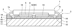
- the terminal 2 projecting from at least one of the side portions 1a to 1d of the electronic component package 1 is provided as an electronic substrate mounting structure on the electronic substrate. 3 is soldered by a reflow method over the land 4 provided on the surface 3. Further, the chip heat radiating member 5 provided on the bottom surface of the electronic component package 1 is superposed on the heat radiating metal pattern 6 provided on the electronic substrate 3 and soldered by a reflow method.
- the electronic component package 1 is obtained by wrapping a semiconductor chip or the like constituting an integrated circuit such as an IC or LSI with a resin for packaging.
- the electronic component package 1 is generally substantially rectangular in plan view.
- the terminals 2 project from a pair of opposing side portions 1a and 1c (see FIG. 1) and two pairs of side portions 1a to 1d (see FIG. 2) in the rectangular electronic component package 1. .
- the electronic substrate 3 has a wiring pattern provided on the surface of the base material 11 with an insulating layer 10 interposed therebetween.
- the land 4 indicates a portion of the wiring pattern that performs solder bonding to the terminal 2.
- the heat dissipation metal pattern 6 indicates a portion of the wiring pattern that performs solder bonding to the chip heat dissipation member 5.
- the land 4 and the heat dissipation metal pattern 6 have an affinity for the molten solder. Therefore, when the solder melts, the solder rises on the land 4 and the heat radiating metal pattern 6 due to surface tension.
- An insulating protective film such as a resist 12 is formed on the surface of the base material 11 other than the wiring pattern.
- This resist 12 has a property of repelling molten solder. Therefore, when excess solder sticks out of the electronic component package 1, the solder balls 13 as shown in FIG. 5 are formed by being repelled by the resist 12.
- the terminals 2 of the electronic component package 1 are placed on the lands 4 and the heat dissipating metal patterns 6 of the electronic substrate 3 coated with the solder paste 14 using a mask (not shown) as shown in FIGS. 3A and 3B in this order.
- solder bonding is performed by installing the chip heat dissipation member 5 so as to be placed thereon, and then melting the solder paste 14 with heat.
- the electronic component package 1 is placed in a slightly floating state on the solder paste 14, and when the solder paste 14 is melted, the electronic component package 1 sinks by its own weight, so that the solder paste pressed by the electronic component package 1 14 is about to overflow to the outside of the electronic component package 1.
- the solder paste 14 is melted by, for example, heating the entire electronic substrate 3 while passing the electronic substrate 3 on which the electronic component package 1 is installed through a reflow furnace using a conveyor or the like. In addition to heating in a reflow furnace, the solder paste 14 can be melted using warm air, heating steam, infrared rays, laser, or the like.
- Solder paste 14 is a mixture of fine solder powder in a paste. When the solder paste 14 is melted, the solder powder contained therein is bonded and grown, whereby solder bonding is performed. In addition, since the paste contains air, the air gathers in the portion where the solder bonding is performed, bubbles are formed, or the bubbles grow and voids 15 such as solder voids as shown in FIG. There is a tendency to become. In addition, although the cause of the void 15 is not completely clarified, in addition to the above, the solder paste is not evenly dispersed in the solder paste 14 and is used as an auxiliary agent for solder bonding. It is also considered that the gas generated by evaporation of the flux does not completely escape. The gap 15 is also formed, for example, when the solder melts in a ring shape and air bubbles are trapped inside.
- the chip heat radiating member 5 is a metal pad called a bottom pad or a heat spreader.
- the chip heat radiating member 5 is flush with or slightly below the bottom surface of the package resin in the electronic component package 1.
- this embodiment has the following configuration.
- the chip heat dissipation member 5 is formed in a size that is surrounded on all sides by the package resin that constitutes the electronic component package 1.
- the heat dissipating metal pattern 6 extends so as to be removed from the electronic component package 1 continuously with the heat dissipating metal pattern 6 so that at least a part of the heat dissipating metal pattern 6 is larger than the electronic component package 1.
- a pattern extension 22 that leads to the outside of the electronic component package 1 is integrally formed.
- the chip heat radiating member 5 is a square heat sink plate in plan view that is installed on the bottom surface of the electronic component package 1 having a square shape in plan view so as to be substantially similar to the electronic component package 1.
- the heat dissipation metal pattern 6 is formed on the circuit pattern of the electronic board 3 for heat dissipation, and is smaller than the electronic component package 1 and larger than the chip heat dissipation member 5 by about one time. It is formed.
- the solder paste 14 is preferably applied in a range smaller than the heat radiating metal pattern 6.
- the pattern extension 22 is intended to guide the excess solder 21 to the outside of the electronic component package 1, and has a width narrower than one side, for example, a short side, of the heat dissipation metal pattern 6.
- the heat radiation metal pattern 6 extends straight.
- the pattern extension portion 22 is extended toward a portion without the land 4.
- the pattern extension 22 extends in a flagpole shape or a handle shape.
- the pattern extension 22 is provided on different side portions 1 b and 1 d different from the side portions 1 a and 1 c provided with the terminals 2 of the electronic component package 1.
- the pattern extension portion 22 is provided at the positions of the corner portions 31a to 31d between the side portions 1a to 1d on which the terminals 2 of the electronic component package 1 are provided.
- the other side portions 1b and 1d in the case of FIG. 1 are, for example, the remaining side portions of the rectangular electronic component package 1 in which the terminals 2 are provided on the pair of opposing side portions 1a and 1c. It is at least one of the pair of side portions 1b and 1d. In this case, the side portion 1d is used, but both the side portion 1b and both the side portions 1b and 1d may be used.
- the corner portions 31a to 31d are, for example, the four corner portions 31a in the rectangular electronic component package 1 in which the terminals 2 are provided on the two opposing side portions 1a to 1d. At least one of ⁇ 31d. In this case, the corner portion 31d is formed.
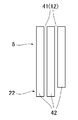
- the heat dissipation metal pattern 6 and the pattern extension portion 22 are provided with a slit portion 41 for suppressing a gap portion.
- the slit portion 41 extends in the extending direction of the pattern extending portion 22 with respect to the heat radiating metal pattern 6 (or in a direction not toward the terminal 2 side).
- the slit part 41 divides the heat radiating metal pattern 6 and the pattern extension part 22 into a plurality of small small areas 42.
- an insulating protective film such as a resist 12 having a property of flipping molten solder is formed on the slit portion 41.
- the melted solder is repelled from the slit portion 41 by the resist 12 in the slit portion 41 and rises on the small regions 42 divided by the slit portion 41 by the surface tension.
- the width of the slit portion 41 is formed at a marginal interval at which molten solder does not move to the adjacent small region 42 via the slit portion 41.
- the width of the slit portion 41 may be slightly narrower than the above, but in this case, the solder on each small region 42 is connected to each other, and the air layer is located at the position of the slit portion 41 in the connected solder. The tunnel will be formed.
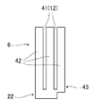
- the shape of the slit portion 41 is formed so as to extend over the entire extending direction of the heat dissipating metal pattern 6 and the pattern extending portion 22, and the heat dissipating metal pattern 6 and the pattern extending portion 22 are formed. Further, it may be completely divided into a plurality of narrow small regions 42 having a substantially strip shape.
- the slit portion 41 is formed so as to extend with respect to part of the extending direction of the radiating metal pattern 6 and the pattern extending portion 22, and the radiating metal pattern 6 and The pattern extension part 22 may be configured to define a plurality of narrow small areas 42 partially connected by the connecting part 43.
- the slit portion 41 has a portion extending in a slightly inclined manner with respect to the extending direction in addition to the extending portion in the extending direction of the heat radiating metal pattern 6 and the pattern extending portion 22.
- the heat radiating metal pattern 6 and the pattern extension 22 may be defined in a plurality of narrow triangular regions 42 having a narrow width that spread toward the outside of the electronic component package 1.
- the mounting structure of the electronic component package 1 is such that the terminals 2 protruding from any one of the side portions 1a to 1d of the electronic component package 1 are overlapped on the lands 4 provided on the electronic substrate 3 and soldered by a reflow method.
- the chip heat radiating member 5 provided on the bottom surface of the electronic component package 1 is superposed on the heat radiating metal pattern 6 provided on the electronic substrate 3 and soldered by the reflow method.
- the heat generated in the electronic component package 1 can be efficiently released to the electronic substrate 3 by soldering the chip heat radiating member 5 to the heat radiating metal pattern 6.
- the pattern extending portion 22 is provided on the heat radiating metal pattern 6.
- the pattern extension portion 22 is provided on the side portions 1b and 1d different from the side portions 1a and 1c provided with the terminals 2 of the electronic component package 1 (FIG. 1).
- the pattern extension portion 22 is provided at the positions of the corner portions 31a to 31d between the side portions 1a to 1d where the terminals 2 of the electronic component package 1 are provided (FIG. 2).
- the pattern extension 22 can be formed on the electronic substrate 3 without interfering with the land 4. Therefore, the excessive solder 21 guided to the pattern extension 22 can be reliably avoided from the land 4.
- a slit portion 41 for suppressing a gap is provided in the heat dissipation metal pattern 6 and the pattern extension portion 22.
- the slit portion 41 divides the heat radiating metal pattern 6 and the pattern extension 22 into a plurality of narrow small regions 42, or the total area of the heat radiating metal pattern 6 and the pattern extension 22 is reduced by the amount of the slit portion 41. It becomes. Therefore, even when the amount of the applied solder paste 14 is small, the melted solder easily spreads over the heat radiating metal pattern 6, so that it is difficult to form the void 15 in the solder. Moreover, since the above-mentioned space
- the gap 15 can be easily driven out along the small area 42 and the slit 41 toward the pattern extension 22. Therefore, it is possible to prevent a decrease in heat dissipation performance (or increase in heat dissipation resistance) due to the presence of the large gap portion 15 and to prevent a temperature rise of the electronic component package 1.
- the small region 42 has an acute triangular shape by providing the slit portion 41 with a slanting extension, the gap 15 is guided from the narrow portion of the small region 42 toward the wide portion. Can do.
- solder balls 13 around the terminals 2 when the amount of the applied solder paste 14 is large by guiding the excessive solder 21 toward the pattern extension portion 22 by the small region 42 and the slit portion 41. Can be more effectively suppressed.
Landscapes
- Engineering & Computer Science (AREA)
- Microelectronics & Electronic Packaging (AREA)
- Manufacturing & Machinery (AREA)
- Physics & Mathematics (AREA)
- Thermal Sciences (AREA)
- Electric Connection Of Electric Components To Printed Circuits (AREA)
- Structures For Mounting Electric Components On Printed Circuit Boards (AREA)
- Structure Of Printed Boards (AREA)
- Cooling Or The Like Of Semiconductors Or Solid State Devices (AREA)
- Structures Or Materials For Encapsulating Or Coating Semiconductor Devices Or Solid State Devices (AREA)
- Cooling Or The Like Of Electrical Apparatus (AREA)
Priority Applications (2)
| Application Number | Priority Date | Filing Date | Title |
|---|---|---|---|
| US15/518,942 US10224261B2 (en) | 2014-10-31 | 2015-09-04 | Electronic component mounting structure |
| CN201580054489.3A CN108029199B (zh) | 2014-10-31 | 2015-09-04 | 电子部件的贴装结构 |
Applications Claiming Priority (2)
| Application Number | Priority Date | Filing Date | Title |
|---|---|---|---|
| JP2014223380A JP6352149B2 (ja) | 2014-10-31 | 2014-10-31 | 電子部品の実装構造 |
| JP2014-223380 | 2014-10-31 |
Publications (1)
| Publication Number | Publication Date |
|---|---|
| WO2016067748A1 true WO2016067748A1 (ja) | 2016-05-06 |
Family
ID=55857094
Family Applications (1)
| Application Number | Title | Priority Date | Filing Date |
|---|---|---|---|
| PCT/JP2015/075194 Ceased WO2016067748A1 (ja) | 2014-10-31 | 2015-09-04 | 電子部品の実装構造 |
Country Status (4)
| Country | Link |
|---|---|
| US (1) | US10224261B2 (https=) |
| JP (1) | JP6352149B2 (https=) |
| CN (1) | CN108029199B (https=) |
| WO (1) | WO2016067748A1 (https=) |
Families Citing this family (6)
| Publication number | Priority date | Publication date | Assignee | Title |
|---|---|---|---|---|
| JP6569610B2 (ja) * | 2016-07-06 | 2019-09-04 | 株式会社デンソー | 電子装置 |
| CN110856338B (zh) * | 2019-10-22 | 2021-03-23 | Tcl华星光电技术有限公司 | 电路板组件及电子设备 |
| CN116491231A (zh) * | 2021-10-29 | 2023-07-25 | 京东方科技集团股份有限公司 | 印刷电路板、其维修方法及显示装置 |
| CN118400989A (zh) * | 2024-05-22 | 2024-07-26 | 深圳宝创电子设备有限公司 | 一种全自动高兼容性精密预烧结贴片设备 |
| WO2026018365A1 (ja) * | 2024-07-17 | 2026-01-22 | Astemo株式会社 | 電力変換装置 |
| WO2026018366A1 (ja) * | 2024-07-17 | 2026-01-22 | Astemo株式会社 | 電力変換装置 |
Citations (6)
| Publication number | Priority date | Publication date | Assignee | Title |
|---|---|---|---|---|
| JPH044779U (https=) * | 1990-04-26 | 1992-01-16 | ||
| JP2004146476A (ja) * | 2002-10-23 | 2004-05-20 | Toyo Commun Equip Co Ltd | 印刷配線基板の構造及びその基板を用いた圧電発振器 |
| JP2005044968A (ja) * | 2003-07-28 | 2005-02-17 | Taiyo Yuden Co Ltd | 回路基板 |
| JP2006303392A (ja) * | 2005-04-25 | 2006-11-02 | Matsushita Electric Ind Co Ltd | プリント配線板と電子回路基板及びその製造方法 |
| JP2008205101A (ja) * | 2007-02-19 | 2008-09-04 | Victor Co Of Japan Ltd | 電子部品実装基板の製造方法及び電子部品実装基板 |
| JP2014075573A (ja) * | 2012-09-14 | 2014-04-24 | Canon Inc | 配線基板およびそれを用いた電子機器 |
Family Cites Families (19)
| Publication number | Priority date | Publication date | Assignee | Title |
|---|---|---|---|---|
| JPH044779A (ja) | 1990-04-20 | 1992-01-09 | Brother Ind Ltd | 画像形成装置 |
| JPH06252285A (ja) * | 1993-02-24 | 1994-09-09 | Fuji Xerox Co Ltd | 回路基板 |
| JP3009176U (ja) * | 1994-09-19 | 1995-03-28 | 船井電機株式会社 | プリント回路基板 |
| JP3308807B2 (ja) * | 1996-04-05 | 2002-07-29 | 電気化学工業株式会社 | 回路基板及びその製造方法 |
| JPH09283567A (ja) * | 1996-04-15 | 1997-10-31 | Nec Corp | Tab式半導体装置及びそのリード位置合わせ方法 |
| US6467972B2 (en) * | 2000-02-29 | 2002-10-22 | Kyocera Corporation | Optical interconnection module |
| JP3639505B2 (ja) * | 2000-06-30 | 2005-04-20 | インターナショナル・ビジネス・マシーンズ・コーポレーション | プリント配線基板及び半導体装置 |
| JP3849573B2 (ja) * | 2001-05-22 | 2006-11-22 | 株式会社日立製作所 | 電子装置 |
| JP4254248B2 (ja) * | 2002-04-05 | 2009-04-15 | 株式会社村田製作所 | 電子装置 |
| US6750538B2 (en) * | 2002-10-24 | 2004-06-15 | Spectra Physics Semiconductor Lasers, Inc. | Heat transfer of solid-state devices |
| JP2005108387A (ja) * | 2003-10-02 | 2005-04-21 | Sankyo Seiki Mfg Co Ltd | 光ヘッド装置、実装用fpc、放熱方法、fpcの製造方法 |
| US20050085007A1 (en) * | 2003-10-20 | 2005-04-21 | Chuong Vu | Joining material stencil and method of use |
| JP4265578B2 (ja) * | 2005-06-30 | 2009-05-20 | オムロン株式会社 | 回路基板 |
| US20080107867A1 (en) * | 2006-11-06 | 2008-05-08 | Fred Miekka | Thermally Conductive Low Profile Bonding Surfaces |
| JP2009105212A (ja) * | 2007-10-23 | 2009-05-14 | Toshiba Corp | プリント配線板および電子機器 |
| WO2009084127A1 (ja) * | 2007-12-28 | 2009-07-09 | Onamba Co., Ltd. | 端子板回路 |
| US8411442B2 (en) * | 2010-09-09 | 2013-04-02 | Texas Instruments Incorporated | Vias in substrate between IC seat and peripheral thermal cage |
| JP2012195546A (ja) | 2011-03-18 | 2012-10-11 | Panasonic Corp | 半導体装置と、その実装体及び製造方法 |
| JP5618419B2 (ja) * | 2011-06-13 | 2014-11-05 | 株式会社日立製作所 | 沸騰冷却システム |
-
2014
- 2014-10-31 JP JP2014223380A patent/JP6352149B2/ja not_active Expired - Fee Related
-
2015
- 2015-09-04 WO PCT/JP2015/075194 patent/WO2016067748A1/ja not_active Ceased
- 2015-09-04 US US15/518,942 patent/US10224261B2/en active Active
- 2015-09-04 CN CN201580054489.3A patent/CN108029199B/zh not_active Expired - Fee Related
Patent Citations (6)
| Publication number | Priority date | Publication date | Assignee | Title |
|---|---|---|---|---|
| JPH044779U (https=) * | 1990-04-26 | 1992-01-16 | ||
| JP2004146476A (ja) * | 2002-10-23 | 2004-05-20 | Toyo Commun Equip Co Ltd | 印刷配線基板の構造及びその基板を用いた圧電発振器 |
| JP2005044968A (ja) * | 2003-07-28 | 2005-02-17 | Taiyo Yuden Co Ltd | 回路基板 |
| JP2006303392A (ja) * | 2005-04-25 | 2006-11-02 | Matsushita Electric Ind Co Ltd | プリント配線板と電子回路基板及びその製造方法 |
| JP2008205101A (ja) * | 2007-02-19 | 2008-09-04 | Victor Co Of Japan Ltd | 電子部品実装基板の製造方法及び電子部品実装基板 |
| JP2014075573A (ja) * | 2012-09-14 | 2014-04-24 | Canon Inc | 配線基板およびそれを用いた電子機器 |
Also Published As
| Publication number | Publication date |
|---|---|
| CN108029199B (zh) | 2020-02-21 |
| JP6352149B2 (ja) | 2018-07-04 |
| CN108029199A (zh) | 2018-05-11 |
| JP2016092138A (ja) | 2016-05-23 |
| US10224261B2 (en) | 2019-03-05 |
| US20170243801A1 (en) | 2017-08-24 |
Similar Documents
| Publication | Publication Date | Title |
|---|---|---|
| JP6352149B2 (ja) | 電子部品の実装構造 | |
| TWI241675B (en) | Chip carrier for semiconductor chip | |
| US10314161B2 (en) | Circuit board and on-board structure of semiconductor integrated circuit | |
| US9237644B2 (en) | Manufacturing of a heat sink by wave soldering | |
| KR102600022B1 (ko) | 전자 소자 모듈 및 그 제조 방법 | |
| TWI390685B (zh) | 半導體元件封裝基板及半導體元件封裝結構 | |
| JP2008147458A (ja) | プリント配線板およびその製造方法 | |
| JP2016092138A5 (https=) | ||
| JP2017175018A (ja) | 半導体装置 | |
| JP6477105B2 (ja) | 半導体装置 | |
| TWI601251B (zh) | 包含不同佈線圖案的覆晶薄膜、包含其之可撓性顯示裝置以及可撓性顯示裝置之製造方法 | |
| JP4821710B2 (ja) | プリント配線板 | |
| JP6907749B2 (ja) | Bgaパッケージ基板、及びbgaパッケージ基板の製造方法 | |
| JP6430894B2 (ja) | 半導体装置及びその製造方法 | |
| JP4312616B2 (ja) | 半導体装置 | |
| JP5062376B1 (ja) | 電子部品実装基板の製造方法 | |
| JP7172663B2 (ja) | 半導体装置 | |
| KR102408126B1 (ko) | 솔더 브릿지를 억제할 수 있는 전기적 패턴을 갖는 전기적 장치 | |
| CN105990300A (zh) | 半导体装置 | |
| JP2007005607A (ja) | 半導体装置 | |
| KR102395374B1 (ko) | Led 실장용 기판, led | |
| JP4114488B2 (ja) | 半導体パッケージの実装構造 | |
| JP2016162813A (ja) | プリント基板及びハンダ付け方法 | |
| JP6488669B2 (ja) | 基板 | |
| JP2009266949A (ja) | プリント配線板 |
Legal Events
| Date | Code | Title | Description |
|---|---|---|---|
| 121 | Ep: the epo has been informed by wipo that ep was designated in this application |
Ref document number: 15854369 Country of ref document: EP Kind code of ref document: A1 |
|
| WWE | Wipo information: entry into national phase |
Ref document number: 15518942 Country of ref document: US |
|
| NENP | Non-entry into the national phase |
Ref country code: DE |
|
| 122 | Ep: pct application non-entry in european phase |
Ref document number: 15854369 Country of ref document: EP Kind code of ref document: A1 |