WO2016056136A1 - 電流検出方法、電流検出装置、電流検出装置の信号補正方法、及び電流検出装置の信号補正装置 - Google Patents
電流検出方法、電流検出装置、電流検出装置の信号補正方法、及び電流検出装置の信号補正装置 Download PDFInfo
- Publication number
- WO2016056136A1 WO2016056136A1 PCT/JP2014/077246 JP2014077246W WO2016056136A1 WO 2016056136 A1 WO2016056136 A1 WO 2016056136A1 JP 2014077246 W JP2014077246 W JP 2014077246W WO 2016056136 A1 WO2016056136 A1 WO 2016056136A1
- Authority
- WO
- WIPO (PCT)
- Prior art keywords
- coefficient
- current detection
- output voltage
- voltage signal
- magnetic field
- Prior art date
- Legal status (The legal status is an assumption and is not a legal conclusion. Google has not performed a legal analysis and makes no representation as to the accuracy of the status listed.)
- Ceased
Links
Images


Classifications
-
- G—PHYSICS
- G01—MEASURING; TESTING
- G01R—MEASURING ELECTRIC VARIABLES; MEASURING MAGNETIC VARIABLES
- G01R15/00—Details of measuring arrangements of the types provided for in groups G01R17/00 - G01R29/00, G01R33/00 - G01R33/26 or G01R35/00
- G01R15/14—Adaptations providing voltage or current isolation, e.g. for high-voltage or high-current networks
- G01R15/20—Adaptations providing voltage or current isolation, e.g. for high-voltage or high-current networks using galvano-magnetic devices, e.g. Hall-effect devices, i.e. measuring a magnetic field via the interaction between a current and a magnetic field, e.g. magneto resistive or Hall effect devices
-
- G—PHYSICS
- G01—MEASURING; TESTING
- G01R—MEASURING ELECTRIC VARIABLES; MEASURING MAGNETIC VARIABLES
- G01R33/00—Arrangements or instruments for measuring magnetic variables
- G01R33/02—Measuring direction or magnitude of magnetic fields or magnetic flux
- G01R33/06—Measuring direction or magnitude of magnetic fields or magnetic flux using galvano-magnetic devices
- G01R33/09—Magnetoresistive devices
-
- G—PHYSICS
- G01—MEASURING; TESTING
- G01R—MEASURING ELECTRIC VARIABLES; MEASURING MAGNETIC VARIABLES
- G01R33/00—Arrangements or instruments for measuring magnetic variables
- G01R33/02—Measuring direction or magnitude of magnetic fields or magnetic flux
- G01R33/06—Measuring direction or magnitude of magnetic fields or magnetic flux using galvano-magnetic devices
- G01R33/09—Magnetoresistive devices
- G01R33/093—Magnetoresistive devices using multilayer structures, e.g. giant magnetoresistance sensors
Definitions
- the present invention relates to a current detection method for detecting a current value by measuring a magnetic field generated by a current flowing through a conductor, a current detection device, a signal correction method for the current detection device, and a signal correction device for the current detection device.
- a magnetic field in a region where the resistance value is relatively linearly changed is selected as a bias magnetic field, and this bias magnetic field is applied to the magnetoresistive effect element to center the bias magnetic field.
- the method of measuring the magnetic field to be measured is adopted within the magnetic field area, but the area where the resistance value changes linearly is narrow, so there is a problem that the range of the magnetic field that can be measured becomes very narrow. ing.
- bias magnetic field applying means for applying a bias magnetic field including a plurality of values to the magnetoresistive effect element is provided.
- the current detection device described in Patent Document 1 merely improves the linearity of the relationship between the magnetic field and the output, that is, the detected magnetic flux density and the output voltage, by changing the bias magnetic field.
- the relationship between the magnetic flux density and the output voltage of the magnetoresistive effect element is still non-linear, and the range in which the magnetic flux density and the output voltage are linearly related (the relationship between the magnetic flux density and the output voltage is linear) Only a range that can be regarded as). Therefore, the range of the magnetic flux density that can be effectively detected using the magnetoresistive effect element becomes narrow, and the degree of freedom when arranging the magnetoresistive effect element may be relatively low.
- the present invention provides a current detection method, a current detection device, a signal correction method for the current detection device, and a signal correction device for the current detection device that can make the relationship of the output voltage to the magnetic flux density substantially linear with high linearity.
- the purpose is to provide.
- the present invention detects a magnetic flux density and detects the magnetic flux density with respect to a current detection device including a magnetic detection element that outputs a voltage signal corresponding to the magnetic flux density.
- the plurality of coefficient groups are calculated by performing arithmetic processing so that an expression indicating the output voltage of the magnetic detection element configured to include each other is fitted to each other, and the magnetic detection element is calculated according to the calculated coefficient groups
- a current detection method is provided that corrects the output voltage signal from the magnetic flux density so as to be substantially linear with respect to the magnetic flux density, and outputs a corrected correction voltage signal.
- the present invention detects a magnetic flux density, outputs a voltage signal corresponding to the magnetic flux density, and supplies the magnetic flux density to the magnetic detection element. Obtained by performing arithmetic processing so that the measured value data indicating the relationship between the obtained magnetic flux density and the output voltage signal and the expression indicating the output voltage of the magnetic detection element including a plurality of coefficient groups are fitted to each other. Signal correction means for correcting the output voltage signal from the magnetic detection element so as to be substantially linear with respect to the magnetic flux density according to the plurality of coefficient groups, and outputting the corrected voltage signal.
- a current detection device is provided.
- the present invention includes a magnetic detection element that detects a magnetic flux density and outputs a voltage signal corresponding to the magnetic flux density, and a storage unit that stores a plurality of coefficient groups.
- a magnetic detection element that detects a magnetic flux density and outputs a voltage signal corresponding to the magnetic flux density
- a storage unit that stores a plurality of coefficient groups.
- the output voltage signal from the magnetic detection element is output as it is, and when the plurality of coefficient groups are stored in the storage unit.
- the present invention provides a magnetic detection device for a current detection device including a magnetic detection element that detects a magnetic flux density and outputs a voltage signal corresponding to the magnetic flux density.
- the plurality of coefficient groups are calculated by performing an arithmetic processing so that an expression indicating the output voltage of the magnetic detection element configured to include the coefficient group is mutually fitted, and from the magnetic detection element according to the plurality of coefficient groups
- the output voltage signal is corrected so as to be substantially linear with respect to the magnetic flux density, and the calculated correction voltage signal is output to the storage unit of the signal correction unit.
- the present invention is connected to a current detection device including a magnetic detection element that detects a magnetic flux density and outputs a voltage signal corresponding to the magnetic flux density, and outputs the output voltage.
- a signal correction device for a current detection device that corrects and outputs a signal, the measurement value data indicating a relationship between a magnetic flux density obtained by supplying a magnetic flux density to the magnetic detection element and an output voltage signal, and a plurality of measurement value data According to the plurality of coefficient groups obtained by performing arithmetic processing so that an expression indicating the output voltage of the magnetic detection element including the coefficient group is fitted to each other, the output voltage signal from the magnetic detection element is Provided is a signal correction device for a current detection device that corrects the magnetic flux density so as to be substantially linear and outputs a corrected correction voltage signal.
- the relationship between the output voltage and the magnetic flux density can be made substantially linear with high linearity.
- FIG. 2 it is a figure which shows schematic structure of the magnetic field generator which applies a to-be-measured magnetic field to an electric current detection apparatus.
- the horizontal axis to be measured magnetic field B and a diagram showing an example of measurement results of the vertical axis the output voltage signal V 1.
- It is a diagram illustrating an example of the output voltage signal V 1 which is substantially linearized the correction signal correcting unit of FIG. 2 is a result of the execution signal correction process.
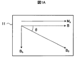
- FIG. 1A is a diagram illustrating a magnetic detection principle of a magnetic detection element used in a current detection method, a current detection device, and a signal correction method of the current detection device according to the first embodiment of the present invention.
- the magnetic detection element 11 is composed of a GMR element.
- Magnetic detection element 11 includes a fixed fixed layer magnetization direction M p, a free layer changes in the magnetization direction ⁇ by the magnetization direction M p and the bias magnetic field is applied in a direction substantially perpendicular to B b and the measured magnetic field B
- the fixed layer and the nonmagnetic layer that separates the free layer are laminated.
- the magnetic field B to be measured is a magnetic field generated by the current to be measured, and ⁇ is the angle of the magnetization direction of the free layer with respect to the magnetization direction M p of the fixed layer.
- the size of the magnitude of the measured magnetic field B is the bias magnetic field B b of the measured magnetic field B
- the angle ⁇ formed by the combined magnetic field B 0 of the bias magnetic field B b and the magnetic field B to be measured and the magnetization direction M p of the fixed layer becomes smaller, and accordingly, the current density in the stacking direction of the fixed layer, the nonmagnetic layer, and the free layer The distribution becomes wider and the resistance value R also becomes lower.
- the application direction of the measured magnetic field B is substantially parallel with the magnetization direction M p opposite direction of the fixed layer, and sufficiently large relative to the size of the magnitude of the bias magnetic field B b of the measured magnetic field B, synthesis
- the angle ⁇ formed by the magnetic field B 0 and the magnetization direction M p of the fixed layer is increased, and accordingly, the current density distribution in the stacking direction of the fixed layer, the nonmagnetic layer, and the free layer is narrowed, and the resistance value R is also increased.
- the magnetization direction of the free layer rotates according to the direction of the combined magnetic field B 0 of the bias magnetic field B b and the measured magnetic field B, and the resistance value of the magnetic detection element 11 changes according to the amount of rotation of the magnetization direction of the free layer.
- the bias magnetic field B b there is a function to suppress the hysteresis of the magnetic sensor 11. Reduces the sensitivity by strong bias magnetic field B b, it can also be expanded linear range as a result.
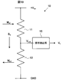
- FIG. 1B is a diagram showing a schematic structure of the current detection device according to the first embodiment of the present invention.
- a current detection device 10 includes a magnetic detection element 11 shown in FIG. 1A and a magnetic detection element 12 having the same structure in series so that the magnetization directions M p1 and M p2 of the fixed layer are opposite to each other. It has a connected half-bridge structure.
- the magnetization direction M p1 of the fixed layer of the magnetic detection element 11 is rightward as indicated by the arrow, and the magnetization direction M p2 of the fixed layer of the magnetic detection element 12 is leftward as indicated by the opposite arrow.
- the directions of these arrows have no relation to the circuit configuration and indicate that the fixed layer magnetization directions of the magnetic detection element 11 and the magnetic detection element 12 are formed in opposite directions for convenience.
- a power supply voltage + V cc (for example, about 5.0 V) is applied to the first electrode of the magnetic detection element 11 of the current detection device 10, and the second electrode of the magnetic detection element 12 is grounded.
- An output voltage signal V out is output from the second electrode of the magnetic detection element 11 and the first electrode of the magnetic detection element 12, which are connection portions between the magnetic detection element 11 and the magnetic detection element 12.
- the signal correction unit 15 performs correction such that the output voltage signal Vout output from the connection portion between the magnetic detection element 11 and the magnetic detection element 12 changes substantially linearly, and outputs a corrected output voltage signal VL .
- a bias magnetic field B b is applied to the magnetic detection elements 11 and 12 in the same direction substantially orthogonal to the magnetization directions M p1 and M p2 , respectively.
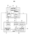
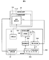
- FIG. 2 is a diagram showing a schematic configuration of a current detection method, a current detection device, and a signal correction method for the current detection device according to the first embodiment of the present invention.
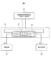
- FIG. 3 is a diagram showing a schematic configuration of the magnetic field generator 20 that applies the measured magnetic field B to the current detector 10 in FIG.
- the input signal correction unit 15 outputs a corrected output voltage signal VL that changes substantially linearly based on a predetermined coefficient.
- the control unit 30 is configured by a control computer having a basic configuration of a personal computer (PC) including a monitor.
- the control unit 30 includes a measured magnetic field constant current source 31, a constant voltage source 32, a voltage measurement unit 34, a fitting coefficient calculation unit 35, and a coefficient control unit 36.
- the magnetic field generator 20 generates the magnetic field B to be measured by the solenoid coil 22 installed in the magnetic shield box 21 and supplies the magnetic field B to be measured to the current detection device 10 installed in the solenoid coil 22. That is, the magnetic field generator 20 may have other configurations as long as it is configured to apply the measured magnetic field B using the current detector 10 as a workpiece.
- the current detection device 10 is configured by storing both the magnetic detection elements 11 and 12 and the signal correction unit 15 in one chip.
- the current detection device 10 is conveyed and installed in the solenoid coil 22 of the magnetic field generator 20 by a handling robot (not shown). At this time, it is installed such that the magnetization directions M p1 and M p2 of the fixed layer of the current detection device 10 and the direction of the magnetic field B to be measured in the solenoid coil 22 are parallel to each other.
- the constant current source 31 for the magnetic field to be measured supplies a predetermined current, for example, a current of about ⁇ 1000 mA to the solenoid coil 22.
- a measured magnetic field B of ⁇ 10 mT is generated in the solenoid coil 22 by the current supplied from the measured magnetic field constant current source 31.
- the controller 30 gradually increases the measured magnetic field B, for example, from ⁇ 10 mT through 0 mT to +10 mT, and gradually from +10 mT through 0 mT to ⁇ 10 mT.
- the current supplied to the solenoid coil 22 from the constant current source for measured magnetic field 31 is controlled so that the measured measured magnetic field B is generated.
- the constant voltage source 32 supplies a power supply voltage of ⁇ V cc (for example, about 5.0 V) to the current detection device 10 mounted in the solenoid coil 22 of the magnetic field generator 20.
- the signal correction unit 15 includes each coefficient (output offset coefficient V off , saturation output coefficient V sat , bias magnetic field strength coefficient B b , angle deviation coefficient ⁇ in the measured magnetic field direction, bias magnetic field direction stored in the storage unit 16. Based on the angle deviation coefficient ⁇ ), the output voltage signal V out from the current detection device 10 is corrected and output as an output voltage signal V 1 .
- the storage unit 16 is provided with a signal correction flag. When the signal correction flag is “0”, it indicates that a predetermined coefficient is not stored, and when the signal correction flag is “1”. Indicates that a predetermined coefficient is stored.
- Signal correcting unit 15 when the signal correction flag is "0", and outputs the output voltage signal V out as it is as the output voltage signal V 1. On the other hand, when the signal correction flag is “1”, the signal correction unit 15 corrects the output voltage signal V out and outputs it as the output voltage signal V 1 . Details of the coefficients stored in the storage unit 16 will be described later.
- the voltage measurement unit 34 outputs the output voltage signal V 1 output from the signal correction unit 15 when the gradually increasing measured magnetic field B is applied, and the signal correction unit 15 outputs the gradually decreasing measured magnetic field B.
- the output voltage signal V 1 is measured, and the average value of the output voltage signals is output to the fitting coefficient calculator 35 as the output voltage signal V 1 .
- a digital multimeter or the like may be provided so that the measured voltage is supplied to the fitting coefficient calculation unit 35 in the control unit 30.
- the fitting coefficient calculation unit 35 uses the current to be measured supplied to the solenoid coil 22 by the constant current source 31 for the magnetic field to be measured, that is, the magnetic field to be measured B applied to the current detection device 10 in the solenoid coil 22 as the horizontal axis.
- the output voltage signal V 1 of the from the current detecting device 10 measured by the measuring unit 34 and the vertical axis to the measurement result (measurement data) by fitting the equation (1) below, the coefficients (output offset coefficient V off , saturation output coefficient V sat , bias magnetic field strength coefficient B b , angle deviation coefficient ⁇ in the measured magnetic field direction, and angle deviation coefficient ⁇ in the bias magnetic field direction are calculated.
- the coefficient control unit 36 includes coefficients (output offset coefficient V off , saturation output coefficient V sat , bias magnetic field strength coefficient B b , angle deviation coefficient ⁇ in the measured magnetic field direction, bias magnetic field direction calculated by the fitting coefficient calculation unit 35. Is written in the storage unit 16 of the signal correction unit 15 and “1” is set in the signal correction flag of the storage unit 16 to indicate the coefficient writing state.
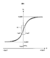
- Figure 4 is a diagram showing an example of a horizontal axis to be measured magnetic field B, the output voltage signal V 1 the vertical axis to the measurement result (measurement data).
- the magnetic field B to be measured varies in the range of ⁇ 10 to +10 mT, for example.
- the output voltage signal V 1 becomes a curve that changes in a range where the lower limit value is about +2.36 V and the upper limit value is about +2.56 V as the measured magnetic field B changes, for example. .
- the range of measured magnetic field B is surrounded by a dotted line rectangle 41 in FIG near about ⁇ 0.5 mT is, the output voltage signal V 1 is a linear range that can be regarded as substantially linearly changed.
- the range of magnetic flux density that can be effectively detected using the magnetoresistive effect element is very narrow, such as ⁇ 1 to +1 mT. Met.
- the range of the output voltage signal V 1 also e.g., narrow as about ⁇ 30 mV.
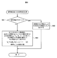
- FIG. 5 is a diagram illustrating an example of signal correction processing executed by the control unit 30 in FIG.
- FIG. 6 is a diagram illustrating an example of signal correction processing executed by the signal correction unit 15 of FIG.
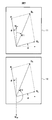
- FIG. 7 is a diagram illustrating the relationship between the magnetic field detection element 11 and the magnetic field detection element 12 in the current detection device 10, the bias magnetic field B b , the magnetic field B to be measured, and the combined magnetic field B 0 .
- Figure 8 is a diagram showing an example of the output voltage signal V 1 which is substantially linearized correction is the result of the signal correction processing signal correcting unit 15 of FIG. 2 is executed.
- step S51 of the signal correction process of the control unit 30 in FIG. 5 the control unit 30 determines that the magnetic field in the solenoid coil 22 of the magnetic field generator 20 from the constant current source 31 for the magnetic field to be measured is the magnetic detection element of the current detection device 10.
- the current increases in the range of about ⁇ 1000 mA so that the magnetic flux density in the range of 11 and 12 can be detected, the current is continuously supplied in the case of the decrease, and as shown in FIG.
- the output voltage signal V 1 from the current detection device 10 with respect to the measurement magnetic field B is measured.
- the signal correction unit 15 since the coefficient has not yet been stored in the storage unit 16 of the signal correction unit 15 and the signal correction flag is “0”, the signal correction unit 15 has a nonlinear function as shown in FIG. and it outputs an output voltage signal V out as it is as the output voltage signal V 1.
- step S52 of the signal correction processing of the control unit 30 of FIG. 5 the fitting coefficient calculation unit 35 in the controller 30, the output voltage signal V 1 of the waveform obtained in step S51, V f of the following formula (1) are applied to the coefficients (output offset coefficient V off , saturation output coefficient V sat , bias magnetic field strength coefficient B b , angle deviation coefficient ⁇ in the direction of the magnetic field to be measured, and angle deviation coefficient ⁇ in the direction of the bias magnetic field) by the least square method.
- the coefficients output offset coefficient V off , saturation output coefficient V sat , bias magnetic field strength coefficient B b , angle deviation coefficient ⁇ in the direction of the magnetic field to be measured, and angle deviation coefficient ⁇ in the direction of the bias magnetic field
- the output offset coefficient V off is an output voltage value at which the nonlinear output voltage signal V 1 as shown in FIG. In the case of FIG. 4, since the lower limit value is about + 2.36V and the upper limit value is about + 2.56V, the output offset coefficient Voff is about + 2.46V.
- the saturation output coefficient V sat is an output voltage value at which the nonlinear output voltage signal V 1 as shown in FIG. 4 indicates an upper limit value and a lower limit value.
- the saturation output coefficient V sat is about 100 mV.
- the magnetization direction M p1 in the fixed layer of the magnetic detection element 11 is upward in the drawing
- the magnetization direction M p2 in the fixed layer of the magnetic detection element 12 is downward in the drawing.
- the bias magnetic field B b is a direction substantially orthogonal to the magnetization directions M p1 and M p2 and is rightward in the drawing.
- the bias magnetic field Bb is generated by providing a magnet for the bias magnetic field in the vicinity of the magnetic detection elements 11 and 12.
- a bias coil (not shown) provided in the current detection device 10 is used in place of the bias magnet, it can be generated by supplying a constant current to the bias coil.
- the bias magnetic field strength coefficient Bb is a bias strength magnetic field generated by the bias magnetic field magnet or the bias coil.
- the current detector 10 is installed in the magnetic field generator 20 so that the magnetization directions M p1 and M p2 of the fixed layer and the direction of the magnetic field B to be measured in the solenoid coil 22 are parallel to each other. May be installed with an angle shift by an angle ⁇ .
- the angle ⁇ formed by the magnetic field to be measured B with respect to the magnetization directions M p1 and M p2 at this time is defined as an angle deviation coefficient ⁇ in the direction of the magnetic field to be measured.
- the angular deviation coefficient ⁇ in the direction of the magnetic field to be measured has a positive value in the counterclockwise direction with reference to the directions of the magnetization directions M p1 and M p2 .
- a bias magnetic field B b is applied to the magnetic detection elements 11 and 12 in the current detection device 10 in a direction substantially orthogonal to the magnetization directions M p1 and M p2 of the fixed layer.
- the angle deviation is caused by the angle ⁇ due to an error or an error (individual difference) in manufacturing the bias coil.
- the angle ⁇ formed by the bias magnetic field B b with respect to the perpendicular line to the magnetization directions M p1 and M p2 at this time is defined as an angle deviation coefficient ⁇ in the baice magnetic field direction.
- the angle deviation coefficient ⁇ in the baice magnetic field direction has a positive value in the counterclockwise direction with reference to a direction perpendicular to the magnetization directions M p1 and M p2 .
- the synthetic magnetic field B 0 obtained by synthesizing the measured magnetic field B and the bias magnetic field B b is the angle ⁇ 1 displaced in the clockwise direction with respect to the magnetization direction M p1
- the current detecting device 10 the combined magnetic field B 0 obtained by combining the magnetic field B to be measured and the bias magnetic field B b is offset by an angle ⁇ 2 in the counterclockwise direction with respect to the magnetization direction M p2 .
- the direction and the magnitude of the combined magnetic field B 0 of the magnetic detection elements 11 and 12 are the same.
- the fitting coefficient calculation unit 35 in the control unit 30 performs, for example, the fitting process over the entire measurement range of ⁇ 10 to +10 mT, thereby performing each coefficient (output offset coefficient V off , saturation output coefficient) of the following equation (1).
- V sat , bias magnetic field strength coefficient B b , angle deviation coefficient ⁇ in the direction of the magnetic field to be measured, and angle deviation coefficient ⁇ in the direction of the bias magnetic field are obtained.
- step S53 of the signal correction process of the control unit 30 in FIG. 5 the coefficient control unit 36 calculates each coefficient (output offset coefficient V off , saturation output coefficient V sat , bias magnetic field strength coefficient B obtained by the fitting coefficient calculation unit 35. b , the angle deviation coefficient ⁇ in the direction of the magnetic field to be measured, and the angle deviation coefficient ⁇ in the direction of the bias magnetic field are written in the storage unit 16 of the signal correction unit 15, and the signal correction flag in the storage unit 16 is set to “1”.
- a current of ⁇ 1000 mA is supplied, and the output voltage signal V 1 output from the current detector 10 for the magnetic field B to be measured is measured.
- the signal correction unit 15 In the storage unit 16 of the signal correction unit 15, “1” is set in the signal correction flag of the storage unit 16 by the above-described step S 53, and each coefficient (output offset coefficient V off , saturation output coefficient V sat , Since the bias magnetic field strength coefficient B b , the angle deviation coefficient ⁇ in the direction of the magnetic field to be measured, and the angle deviation coefficient ⁇ in the direction of the magnetic field to be measured are stored, the signal correction unit 15 outputs a nonlinear output voltage signal as shown in FIG. against V out, it performs signal correction processing of the signal correcting unit 15 of FIG. 6, and outputs an output voltage signal V 1 which is substantially linearized correction as shown in FIG.
- step S55 in the signal correction processing of the control unit 30 of FIG. 5 whether or not the output voltage signal V 1 which is substantially linearized correction is output from the signal correcting unit 15 is changed substantially linearly, i.e. either substantially linear It is determined whether or not it is substantially linear (yes), the process proceeds to step S56, and if it is not substantially linear (no), the process proceeds to step S57.
- the output voltage signal V 1 that has been substantially linearized and corrected by the signal correction unit 15 is substantially linear in a wide range surrounded by a dotted rectangle 42 in which the range of the magnetic field B to be measured is about ⁇ 5 mT. Linearly changing.
- the range of the output voltage signal V 1 can be for example, understood that in the enlarged view of ⁇ 3.7V.
- step S56 of the signal correction process of the control unit 30 in FIG. 5 since it was determined to be linear (yes) in the previous step S55, the range of the measured magnetic field ⁇ B that can be considered to change substantially linearly, For example, about ⁇ 5 mT is written in the storage unit 16, and a series of signal correction processing is completed.
- step S57 of the signal correction process of the control unit 30 in FIG. 5 since it was determined that the signal was not linear (no) in the previous step S55, the measurement range was limited to perform the fitting process again. The process returns to S52.
- the fitting coefficient calculation unit 35 in the control unit 30 performs the fitting process over the entire measurement range of ⁇ 10 to +10 mT, but if it is determined that it is not linear (no) in the process of step S55.
- the measurement range is limited to, for example, ⁇ 8 to +8 mT, and each coefficient (output offset coefficient V off , saturation output coefficient V sat , bias magnetic field strength coefficient B b , measured field) of equation (1)
- the angle deviation coefficient ⁇ in the direction and the angle deviation coefficient ⁇ in the bias magnetic field direction are obtained again.
- the linearity of the measured magnetic field B in the vicinity of about ⁇ 5 mT is improved. Therefore, for example, when the entire measurement range is ⁇ 10 to +10 mT, the next measurement range is ⁇ 9 to +9 mT, the next limited range is ⁇ 8 to +8 mT, and the measurement range is limited at a predetermined ratio. Is desirable.
- the control unit 30 extracts a measurement range that can be regarded as linear, and uses the extracted measurement range as a current detection device. Ten measurable ranges may be written in the storage unit 16 and a series of signal correction processes may be terminated. By reading the measurement range stored in the storage unit 16, the measurable range of the current detection device 10 can be easily recognized.
- the signal correction unit 15 replaces the V f of formula (1) to V 1, the following formula in the case of the synthetic magnetic field B 0 as a function of V 1 (B 0 (V 1)) and (2) pre I remember it.
- V L m ⁇ B 0 (V 1 ) + n (2)
- the signal correction processing executed by the signal correction unit 15 is performed using the equations (2) and the coefficients stored in the storage unit 16 (output offset coefficient V off , saturation output coefficient V sat , bias magnetic field strength coefficient B b , Based on the angle deviation coefficient ⁇ in the measurement magnetic field direction and the angle deviation coefficient ⁇ in the bias magnetic field direction, the output voltage signal Vout is substantially linearly corrected, and the corrected correction voltage signal V L as shown in FIG. as the output voltage signal V 1.
- FIG. 9 is a diagram showing a schematic configuration of a current detection method, a signal correction method of the current detection device, and a signal correction device of the current detection device according to the second embodiment of the present invention, and corresponds to FIG.
- the configurations of the current detection device 10A and the control unit 30A are different from those of the current detection device 10 and the control unit 30 according to the first embodiment, and other configurations are the same as those of the first embodiment. It is common.
- the configuration of the current detection device 10A and the control unit 30A which are the differences, will be described with emphasis, and the components common to those described in the first embodiment will be denoted by common reference numerals. The description is omitted.
- a current detection device 10A is configured by housing magnetic detection elements 11 and 12 having a half bridge structure on one chip.
- the current detection device 10A directly outputs the output voltage signal Vout from the connection part of the half bridge structure. Since the current detection device 10A does not include the signal correction unit 15 as shown in FIG. 2, in the second embodiment, a signal correction device 15A corresponding to the current detection device 10A is created and is used as the current detection device. Connect to 10A.
- the signal correction device 15A has the same configuration as that of the signal correction unit 15 of the first embodiment, receives the output voltage signal Vout output from the current detection device 10A, and is substantially based on a predetermined coefficient. A corrected output voltage signal V L that changes linearly is output.
- the signal correction device of the current detection device changes the output voltage signal Vout output from the current detection device 10A substantially linearly based on a predetermined coefficient.
- This is a signal correction device dedicated to the current detection device 10A that outputs the corrected output voltage signal VL , and is configured by a single element housed on a chip different from the current detection device 10A.
- control unit 30A includes a measured magnetic field constant current source 31, a constant voltage source 32, a voltage measurement unit 34A, a fitting coefficient calculation unit 35A, and a coefficient control unit 36A.
- the configurations of the constant current source 31 for the magnetic field to be measured and the constant voltage source 32 are the same as those in the first embodiment.
- Voltage measuring unit 34A outputs the output voltage signal V out output from the current detection device 10A directly to the input end of the signal correction device 15A, inputs the corrected output signal V 1 that is output along with it from the signal compensation unit 15A and obtains the horizontal axis the measured magnetic field B as shown in FIG. 4, the output voltage signal V 1 the vertical axis to the measurement result (measurement value data).
- the voltage measurement unit 34A outputs the output voltage signal V out output from the current detection device 10A when the gradually increasing measured magnetic field B is applied, and the current detection device 10A when the gradually decreasing measured magnetic field B is applied. measuring the output voltage signal V out output from the outputs to the fitting coefficient calculator 35A and the average value of the output voltage signal V out as an output voltage signal V 1.
- the signal correction device 15A is connected to the voltage measurement unit 34A, the coefficient control unit 36A, and the like in the control unit 30A through chip connection means provided in the control unit 30A.
- Signal correction unit 15A based on the coefficients (A1 ⁇ A5) stored in the storage unit 16A, the correction is added to the output voltage signal V out from the current detection device 10A, it outputs it as an output voltage signal V 1 To do.
- the storage unit 16A is provided with a signal correction flag. When this signal correction flag is “0”, it indicates that a predetermined coefficient is not stored, and when the signal correction flag is “1”. Indicates that a predetermined coefficient is stored.
- Signal correction unit 15A a signal correction flag is a case of "0”, and outputs the output voltage signal V out from the voltage measuring unit 34A as it is as the output voltage signal V 1 to the voltage measuring unit 34A.
- the signal correction unit 15A if the signal correction flag is "1", correction is added to the output voltage signal V out from the voltage measuring unit 34A, and outputs the voltage measuring unit 34A it as an output voltage signal V 1 . Details of the coefficients (A1 to A5) stored in the storage unit 16A will be described later.
- the fitting coefficient calculator 35A uses the current to be measured supplied to the solenoid coil 22 by the constant current source 31 for the magnetic field to be measured, that is, the magnetic field B to be measured applied to the current detection device 10 in the solenoid coil 22 as the horizontal axis. the measurement results of the output voltage signal V 1 of the the measured current detector 10A by the measuring unit 34A and the vertical axis, and the arithmetic processing so as to fit to the following equation (3), the coefficients (A1 ⁇ A5) calculate.
- the coefficient A1 is V off in the equation (1)
- the coefficient A2 is 2 ⁇ B b ⁇ sin ( ⁇ ) which is a coefficient of the combined magnetic field B 0 in the route of the equation (1).
- the coefficient A3 is the square of B b in the route of the expression (1)
- the coefficient A4 is V sat ⁇ cos ⁇ that is the coefficient of the combined magnetic field B 0 on the upper side of the expression (1)
- the coefficient A5 is the expression (1) corresponds to B b ⁇ V sat ⁇ sin ⁇ on the upper side.
- the coefficients A1 to A5 are respectively the output offset coefficient V off , the saturated output coefficient V sat , the bias magnetic field strength coefficient B b , the angle deviation coefficient ⁇ in the measured magnetic field direction, and the angle deviation coefficient ⁇ in the bias magnetic field direction.
- the equations (1) and (3) are substantially the same.
- the fitting coefficient calculation unit 35A fits V f in Expression (3) to the waveform of the output voltage signal V 1 over the entire measurement range of, for example, ⁇ 10 to +10 mT.
- the coefficients A1 to A5 are obtained by the method of least squares.
- the fitting coefficient calculation unit 35A only needs to simply obtain the coefficients, so that the calculation process can be simplified and speeded up.
- the coefficient control unit 36A writes the coefficients A1 to A5 of the equation (3) obtained by the fitting coefficient calculation unit 35A to the storage unit 16A of the signal correction device 15A and sets “1” to the signal correction flag of the storage unit 16A. To do.
- the coefficient control unit 36A specifies the chip of the current detection device 10A whose signal has been corrected.
- the ID number to be stored may be stored in the storage unit 16A. As a result, the current detection device 10A and the signal correction device 15A can be associated one to one.
- the signal correction process executed by the control unit 30A of FIG. 9 and the signal correction process executed by the signal correction device 15A of FIG. 9 according to the second embodiment are performed by the coefficients A1 to A5 obtained by the fitting coefficient calculation unit 35A. Except for the difference, since it is common to the above-described FIG. 5 and FIG. 6, description thereof is omitted.
- a current that does not have a current detection device or a signal correction unit that is already installed on the measurement object can be applied to a detection device.
- the signal correction device 15A can be connected to an existing current detection device or the like in a motor drive unit or a solar battery of a hybrid vehicle or an electric vehicle, and the output signal can be corrected as appropriate.
- the magnetic detection elements 11 and 12 having the half bridge structure have been described as an example.
- the present invention is not limited to this, and a full bridge structure in which four magnetic detection elements are connected in a bridge shape. It may be configured by one magnetic detection element.
- control units 30 and 30A are control computers having a personal computer (PC) as a basic configuration
- PC personal computer
- the control units 30 and 30A are one-chip microcomputers. It may be configured.
- the magnetic field generator 20 provided with the solenoid coil 22 has been described as an example.
- a magnetic flux density for measurement can be generated by passing a predetermined current through the object to be measured.
- the control units 30 and 30A can cope with this by outputting a signal for current control to the object to be measured.
- the signal correction unit 15 / signal correction device 15A includes coefficients (output offset coefficient V off , saturation output coefficient V sat , bias magnetic field strength coefficient B b , measured magnetic field direction, and the like stored in the storage unit 16 / 16A. angular deviation coefficient of phi, based on the angle displacement coefficient ⁇ / A1 ⁇ A5) of the bias magnetic field direction, the correction is added to the output voltage signal V out from the current detection unit 10, and outputs it as an output voltage signal V 1.
- Fitting coefficient calculation unit 35 / 35A of the control section 30 / the 30A since V f of formula (1) to the output voltage signal V 1 of the waveform is seeking the coefficients to fit by a least square method , the signal correction section 15 / signal correcting device 15A correction voltage signal V 1 output from the relationship of the output voltage to the magnetic flux density becomes as very exhibit high approximately linear linearity, further correction voltage range of the signal V 1 Can also be enlarged.
- the output offset coefficient V off is an output voltage value at which the nonlinear output voltage signal V 1 as shown in FIG. 4 is point-symmetric, and the saturation output coefficient V sat is shown in FIG. nonlinear output voltage signal V 1 is the upper limit value and the lower limit output voltage value indicating shown
- the bias magnetic field intensity coefficient B b is the bias intensity magnetic field generated by the bias field magnet or bias coil, of the measured magnetic field direction
- the angle deviation coefficient ⁇ is the angle formed by the magnetic field to be measured B with respect to the magnetization directions M p1 and M p2
- the angle deviation coefficient ⁇ in the bias magnetic field direction is the bias magnetic field B with respect to the orthogonal line with respect to the magnetization directions M p1 and M p2 .
- the signal correction processing executed by the signal correction unit 15 / signal correction device 15A is performed by the equation (2) and the coefficients stored in the storage unit 16 / 16A (output offset coefficient V off , saturation output coefficient V sat , bias magnetic field intensity coefficient B b, the angular deviation coefficient of the measured magnetic field direction phi, based on the angle deviation coefficient alpha) of the bias magnetic field direction, the output voltage signal V out is substantially linearized correction, the corrected voltage signal V L and outputs as an output voltage signal V 1.
- the formula (2) replacing the V f of the equation (1) to V 1, since the synthetic magnetic field B 0 is using a function of V 1 (B 0 (V 1)), the signal correction correction voltage signal V 1 output from the section 15, as an output close to substantially linearly exhibit higher linearity.
- the signal correction processing executed by the signal correction unit 15A is performed by linearly correcting the output voltage signal Vout based on the equation (3) and the coefficients (A1 to A5) stored in the storage unit 16.
- the corrected voltage signal V L is output as the output voltage signal V 1 .
- the coefficient A1 constituting the expression (3) is V out of the expression (1)
- the coefficient A2 is 2 ⁇ B b ⁇ sin (the coefficient of the combined magnetic field B 0 in the route of the expression (1). ⁇ )
- the coefficient A3 is the square of B b in the route of Equation (1)
- the coefficient A4 is the coefficient of V sat ⁇ cos ⁇ that is the coefficient of the combined magnetic field B 0 on the upper side of Equation (1). Since A5 corresponds to B b ⁇ V sat ⁇ sin ⁇ on the upper side of the expression (1), the correction voltage signal V 1 output from the signal correction unit 15A is almost linear indicating higher linearity. Output.
- Unit 15 / signal correction device 15A includes each coefficient (output offset coefficient V off , saturation output coefficient V sat , bias magnetic field strength coefficient B b , angle deviation coefficient ⁇ in the measured magnetic field direction) stored in the storage unit 16 / 16A.
- the correction is added to the output voltage signal V out from the current detection unit 10 / 10A, are output as the correction voltage signal V 1 Since, the correction voltage signal V 1 was, as an output close to substantially linearly exhibit higher linearity.
- the output voltage signal Vout output from the current detection device 10A is set to a predetermined coefficient by using a signal correction device 15A housed on a chip different from the current detection device 10A.
- a signal correction device 15A housed on a chip different from the current detection device 10A.
- the measurement range of the current detection device 10 / 10A can be easily confirmed. be able to.
- the magnetic flux density (B) and the output voltage of the current detection device (10 / 10A) obtained by supplying the magnetic flux density (B) in a range that can be detected by the magnetic detection elements (11, 12).
- Measured value data indicating the relationship with the signal (V 1 ) is acquired, and the acquired measured value data and a plurality of coefficient groups (V off , V sat , B b , ⁇ , ⁇ / A1 to A5) are included.
- the plurality of coefficient groups (V off , V sat , B b , ⁇ , ⁇ / A1 ⁇ ) are obtained by performing arithmetic processing so that the expression indicating the output voltage of the magnetic detection element (11, 12) is fitted to each other. A5) is calculated and before calculated A plurality of coefficient groups (V off, V sat, B b, ⁇ , ⁇ / A1 ⁇ A5) according to the output voltage signal from the magnetic sensing element (11, 12) to (V 1) to the magnetic flux density (B)
- a current detection method that corrects the signal to be substantially linear and outputs a corrected voltage signal (V L ).
- both the magnetic detection elements (11, 12) and the signal correction unit (15) are housed in one chip, or the current detection device (10) or the magnetic detection elements (11, 11) are configured.
- a predetermined magnetic flux density (B) is supplied to the current detection device (10A) configured by storing only 12) on one chip, and the magnetic flux density (B) and the output of the current detection device (10 / 10A)
- the measurement value data indicating the relationship with the voltage signal (V 1 ) is acquired, and using the acquired measurement value data, calculation processing is performed so that the predetermined equation (1) or equation (3) is fitted to each other, and the coefficient A group (V off , V sat , B b , ⁇ , ⁇ / A1 to A5) is calculated, and according to the calculated coefficient group, the magnetic detection element (11) is used using the signal correction unit (15) or the signal correction device (15A).
- magnetic output voltage signal from 12) (V 1) It is obtained as corrected so as to be substantially linear, and outputs the correction voltage signal (V L) relative density (B).
- V L correction voltage signal
- the relationship of the output voltage (V 1 ) to the detected magnetic flux density (B) can be made substantially linear with high linearity.
- An expression indicating the output voltage of the magnetic detection element (11, 12) including a plurality of coefficient groups (V off , V sat , B b , ⁇ , ⁇ / A1 to A5) is The current detection method according to [1], wherein the coefficients A1 to A5 are calculated such that an output voltage expressed by the equation is fitted to the measured value data.
- This current detection method uses equation (3) when performing arithmetic processing so as to fit to measured value data.
- each coefficient is modified so that the expression (1) becomes a function of the combined magnetic field B 0 , and expressed as coefficients A1 to A5 in the expression (3).
- coefficients A1 to A5 depend on the coefficient group (V off , V sat , B b , ⁇ , ⁇ ) of the equation (1), show the same result, and are purely as coefficients (A1 to A5) Since the calculation can be performed, the coefficient can be easily calculated using existing spreadsheet software or the like.
- the coefficient A1 constituting the above equation is the output offset coefficient V off , the coefficient A2 is 2 ⁇ B b ⁇ sin ( ⁇ ), the coefficient A3 is the square of B b , the coefficient A4 is V sat ⁇ cos ⁇ , and the coefficient A5 Is Bb ⁇ Vsat ⁇ sin ⁇ , and in the coefficients A2 to A5, V sat is the saturation output coefficient, B b is the bias magnetic field strength coefficient, ⁇ is the angle deviation coefficient in the measured magnetic field direction, and ⁇ is the angle deviation in the bias magnetic field direction.
- the current detection method according to [2] wherein the current detection method is a coefficient.
- each coefficient (V off , V sat , B b , ⁇ , ⁇ ) constituting the equation (1) corresponds to the actual structure of the magnetic detection element (11, 12), it is fitted to the measured value data.
- the signal correcting section (15) / signal correction apparatus correcting voltage signal V 1 output from the (15A) becomes the output close to substantially linearly exhibit higher linearity.
- the signal correction unit (15 / 15A) outputs from the magnetic detection elements (11, 12) based on the coefficient groups (V off , V sat , B b , ⁇ , ⁇ / A1 to A5).
- An arithmetic expression for correcting the voltage signal (V 1 ) is specifically shown as Expression (2).
- This expression (2) replaces the output voltage signal V f of the expression (1) or (3) with the output voltage signal V 1 , and the combined magnetic field B 0 is a function (B 0 (V 1 ) of the output voltage signal V 1. ).
- a magnetic detection element (11, 12) that detects a magnetic flux density (B) and outputs a voltage signal (V out ) corresponding to the magnetic flux density (B), and the magnetic detection element (11, 12).
- Measurement value data indicating the relationship between the magnetic flux density (B) obtained by supplying the magnetic flux density (B) and the output voltage signal (V 1 ), and a plurality of coefficient groups (V off , V sat , B b , ⁇ ) , ⁇ / A1 to A5) including the plurality of coefficient groups (V off) obtained by performing arithmetic processing so that the equations indicating the output voltages of the magnetic detection elements (11, 12) are fitted to each other.
- the output voltage signal (V 1 ) from the magnetic detection element (11, 12) is substantially linear with respect to the magnetic flux density (B).
- a (10 / 10A) To the corrected correction voltage signal ( Current detecting device provided with signal correcting means for outputting a L) and (15 / 15A), a (10 / 10A). This current detection device (10 / 10A) corresponds to the current detection method described in [1].
- the coefficient A1 constituting the above equation is the output offset coefficient V off , the coefficient A2 is 2 ⁇ B b ⁇ sin ( ⁇ ), the coefficient A3 is the square of B b , the coefficient A4 is V sat ⁇ cos ⁇ , and the coefficient A5 Is Bb ⁇ Vsat ⁇ sin ⁇ , and in the coefficients A2 to A5, V sat is the saturation output coefficient, B b is the bias magnetic field strength coefficient, ⁇ is the angle deviation coefficient in the measured magnetic field direction, and ⁇ is the angle deviation in the bias magnetic field direction.
- the current detection device (10 / 10A) according to [6], which is a coefficient. This current detection device (10 / 10A) corresponds to the current detection method described in [3] above.
- the correction voltage signal (V L ) is output in accordance with the plurality of coefficient groups (V off , V sat , B b , ⁇ , ⁇ / A1 to A5) obtained by the current according to [6] Detection device (10 / 10A). This current detection device (10 / 10A) corresponds to the current detection method described in [4].
- a magnetic detection element (11, 12) that detects a magnetic flux density (B) and outputs a voltage signal (V out ) corresponding to the magnetic flux density (B), and a plurality of coefficient groups (V off , V sat).
- B b , ⁇ , ⁇ / A1 to A5) are stored, and the plurality of coefficient groups (V off , V sat , B b , ⁇ , ⁇ ) are stored in the storage unit (16).
- / A1 to A5) are not stored, the output voltage signal (V 1 ) from the magnetic detection element (11, 12) is output as it is, and the plurality of coefficient groups (16) are stored in the storage unit (16).
- V off , V sat , B b , ⁇ , ⁇ / A1 to A5) are stored, according to the plurality of coefficient groups (V off , V sat , B b , ⁇ , ⁇ / A1 to A5)
- the output voltage signal (V 1 ) from the magnetic detection element (11, 12) is converted into the magnetic flux.
- a current detection device (10) comprising signal correction means (15) for correcting the density (B) so as to be substantially linear and outputting a corrected voltage signal (V L ),
- the plurality of coefficient groups (V off , V sat , B b , ⁇ , ⁇ / A1 to A5) are not stored in the storage unit (16) of the signal correction unit (15)
- the magnetic detection element (11, 12) supplies a magnetic flux density (B) within a detectable range, and the magnetic flux density (B) obtained thereby and the output voltage signal (V) of the current detection device (10).
- the measurement value data indicating the relationship with the above is acquired, and includes the acquired measurement value data and a plurality of coefficient groups (V off , V sat , B b , ⁇ , ⁇ / A1 to A5).
- the expression indicating the output voltage of the magnetic detection elements (11, 12) is mutually Wherein by performing arithmetic processing as potting a plurality of coefficient groups (V off, V sat, B b, ⁇ , ⁇ / A1 ⁇ A5) is calculated, the calculated plurality of coefficient groups (V off, V sat , B b , ⁇ , ⁇ / A1 to A5) are stored in the storage unit (16) of the signal correction means (15), the signal correction method of the current detection device (10).
- the signal detection method of the current detection device (10) includes a current detection device (10) configured such that both the magnetic detection elements (11, 12) and the signal correction unit (15) are housed in one chip. , Supplying a predetermined magnetic flux density (B), obtaining measurement value data indicating the relationship between the magnetic flux density (B) and the output voltage signal (V 1 ) of the current detection device (10), and obtaining the obtained measurement value data. To calculate the coefficient group (V off , V sat , B b , ⁇ , ⁇ / A1 to A5) by performing arithmetic processing so that the predetermined formula (1) or formula (3) is fitted to each other.
- the signal correction unit (15) is used to correct the output voltage signal (V 1 ) from the magnetic detection elements (11, 12) so as to be substantially linear with respect to the magnetic flux density (B).
- a correction voltage signal (V L ) is output.
- the current detection device After storing the plurality of coefficient groups (V off , V sat , B b , ⁇ , ⁇ / A1 to A5) in the storage unit (16) of the signal correction unit (15), the current detection device The correction voltage signal (V L ) obtained by supplying the magnetic flux density (B) in a range that can be detected by the magnetic detection element (11, 12) to (10) and measuring the correction It is determined whether or not the voltage signal (V L ) is substantially linear. When the voltage signal (V L ) is substantially linear, the measurement range based on the magnetic field to be measured is stored in the storage unit (16).
- the calculation process is executed again by limiting the range of the magnetic field to be measured to calculate the plurality of coefficient groups (V off , V sat , B b , ⁇ , ⁇ / A1 to A5), and the calculated plurality Coefficient group (V off , V sat , B b , ⁇ , ⁇ / A1 to A5)
- the signal correction method of the current detection device (10) according to [9], wherein the limited range of the magnetic field to be measured is stored in the storage unit (16) of the signal correction unit (15).
- Signal correcting method of the current detecting device (10) is whether or not the output voltage signal V 1 which is substantially linearized correction is output from the signal correction section (15) changes substantially linearly, i.e.
- the measured magnetic field range ⁇ B that can be considered to change substantially linearly is written in the storage unit (16), and is not linear (no) ), The measurement range is limited and the fitting process is performed again. Thereby, the correction voltage signal V 1 was, as an output close to substantially linearly exhibit higher linearity.
- the measurement range of the current detection device (10) can be easily confirmed. be able to.
- a current detection device (10A) including a magnetic detection element (11, 12) that detects a magnetic flux density (B) and outputs a voltage signal ( Vout ) corresponding to the magnetic flux density (B).
- the magnetic flux density (B) and the output voltage signal (V 1 ) of the current detection device (10A) obtained by supplying the magnetic flux density (B) in a range that can be detected by the magnetic detection elements (11, 12).
- Is obtained, and the obtained measurement value data and a magnetic field including a plurality of coefficient groups (V off , V sat , B b , ⁇ , ⁇ / A1 to A5) are acquired.
- the plurality of coefficient groups (V off , V sat , B b , ⁇ , ⁇ / A1 to A5) are calculated by performing arithmetic processing so that the expressions indicating the output voltages of the detection elements (11, 12) are fitted to each other. And the plurality of coefficient groups (V o ff , V sat , B b , ⁇ , ⁇ / A1 to A5) so that the output voltage signal (V 1 ) from the magnetic detection element (11, 12) is substantially linear with respect to the magnetic flux density (B).
- the signal correction means (15A) that outputs the corrected voltage signal (V L ) to the calculated coefficient group (V off , V sat , B b , ⁇ , ⁇ / A1 to A5), and the signal correcting means (V off , V sat , B b , ⁇ , ⁇ / A1 to A5) are stored in the storage unit (16A).
- 15A) is used as a signal correction device (15A) of the current detection device (10A), the signal correction method of the current detection device (10A).
- This signal correction method of the current detection device (10A) uses a signal correction device 15A housed on a chip different from the current detection device 10A, and outputs an output voltage signal V out output from the current detection device 10A to a predetermined value. Is output as a corrected output voltage signal VL that changes substantially linearly based on the coefficient of the signal.
- the signal correction method is the same as the method described in [9]. As a result, the output voltage (V 1 ) with respect to the detected magnetic flux density (B) can be detected even for the current detection device (10A) that has already been installed on the object to be measured and the current detection device (10A) that does not have a signal correction unit. It becomes possible to make the relationship substantially linear with high linearity.
- the current detection device After storing the plurality of coefficient groups (V off , V sat , B b , ⁇ , ⁇ / A1 to A5) in the storage unit (16A) of the signal correction unit (15A), the current detection device The correction voltage signal (V L ) obtained by supplying the magnetic flux density (B) in a range detectable by the magnetic detection element (11, 12) to (10A) and measuring the correction It is determined whether or not the voltage signal (V L ) is substantially linear. When the voltage signal (V L ) is substantially linear, the measurement range based on the magnetic field to be measured is stored in the storage unit (16A).
- the calculation process is executed again by limiting the range of the magnetic field to be measured to calculate the plurality of coefficient groups (V off , V sat , B b , ⁇ , ⁇ / A1 to A5), and the calculated plurality Coefficient group (V off , V sat , B b , ⁇ , ⁇ / A1 To A5) and the limited range of the magnetic field to be measured are stored in the storage unit (16A) of the signal correction means (15A), and the plurality of coefficient groups (V off , V sat , B b , ⁇ , ⁇ / A1 to A5) and the signal correction means (15A) in which the limited range of the magnetic field to be measured is stored in the storage unit (16A) are used as the signal correction device (15A) of the current detection device (10A).
- the signal correction method for the current detection device (10A) according to [11]. This signal correction method of the current detection device (10A) corresponds to the signal correction method of the current detection device (10) described in [10].
- An equation indicating the output voltage of the magnetic detection element configured to include a plurality of coefficient groups is: The current detection device according to any one of [9] to [13], wherein the coefficients A1 to A5 are calculated such that the output voltage Vf of this equation is fitted to the measured value data. 10 / 10A) signal correction method.
- the signal correction method of the current detection device (10 / 10A) corresponds to the current detection method described in [2].
- the coefficient A1 constituting the above equation is the output offset coefficient V off , the coefficient A2 is 2 ⁇ B b ⁇ sin ( ⁇ ), the coefficient A3 is the square of B b , the coefficient A4 is V sat ⁇ cos ⁇ , and the coefficient A5 Is Bb ⁇ Vsat ⁇ sin ⁇ , and in the coefficients A2 to A5, V sat is the saturation output coefficient, B b is the bias magnetic field strength coefficient, ⁇ is the angle deviation coefficient in the measured magnetic field direction, and ⁇ is the angle deviation in the bias magnetic field direction.
- the signal correction method of the current detection device (10 / 10A) according to [13], which is a coefficient.
- the signal correction means of the current detection device (10 / 10A) (15 / 15A) is replaced by the output voltage V f in the formula (1) to the output voltage V 1, the output voltage of the synthesized magnetic field B 0
- V f the output voltage of the synthesized magnetic field B 0
- V L m ⁇ B 0 (V 1 ) + n (where m is an arbitrary value other than 0, and n is an arbitrary value)
- the correction voltage signal (V L ) is output in accordance with the plurality of coefficient groups (V off , V sat , B b , ⁇ , ⁇ / A1 to A5) calculated by the arithmetic processing.
- the signal correction method of the current detection device (10 / 10A) according to [13] or [14].
- the signal correction method of the current detection device (10 / 10A) corresponds to the current detection method described in [3].
- a current detection device (10 / 10A) including a magnetic detection element (11, 12) that detects a magnetic flux density (B) and outputs a voltage signal ( Vout ) corresponding to the magnetic flux density (B).
- a signal correction device (15A) of a current detection device (10A) that is connected and corrects and outputs the output voltage signal (V 1 ), and applies a magnetic flux density (B) to the magnetic detection elements (11, 12).
- Measured value data indicating the relationship between the magnetic flux density (B) obtained by the supply and the output voltage signal (V 1 ), and a plurality of coefficient groups (V off , V sat , B b , ⁇ , ⁇ / A1 to A5) ) Including the plurality of coefficient groups (V off , V sat , B b) obtained by performing arithmetic processing so as to fit the expression indicating the output voltage of the magnetic detection element (11, 12) including each other.
- the output voltage signal (V 1) from the magnetic sensing element (11, 12) is corrected so as to be substantially linear with respect to the magnetic flux density (B), the corrected correction voltage signal (V L) A signal correction device (15A) of the current detection device (10A) for outputting.
- the signal correction device (15A) of the current detection device (10A) corresponds to the signal correction method of the current detection device (10A) described in [11].
- An expression indicating the output voltage of the magnetic detection element including a plurality of coefficient groups is The signal correction device (15A) of the current detection device (10A) according to [16], wherein the coefficients A1 to A5 are calculated so that the output voltage Vf of this equation is fitted to the measurement value data. .
- the signal correction device (15A) of the current detection device (10A) corresponds to the current detection method described in [3] and the signal correction method of the current detection device (10A) described in [13]. is there.
- the coefficient A1 constituting the above equation is the output offset coefficient V off , the coefficient A2 is 2 ⁇ B b ⁇ sin ( ⁇ ), the coefficient A3 is the square of B b , the coefficient A4 is V sat ⁇ cos ⁇ , and the coefficient A5 Is Bb ⁇ Vsat ⁇ sin ⁇ , and in the coefficients A2 to A5, V sat is the saturation output coefficient, B b is the bias magnetic field strength coefficient, ⁇ is the angle deviation coefficient in the measured magnetic field direction, and ⁇ is the angle deviation in the bias magnetic field direction.
- Signal correction device (15A) The signal correction device (15A) of the current detection device (10A) corresponds to the current detection method described in [4] and the signal correction method of the current detection device (10A) described in [14
- V off ... Output offset coefficient V sat ... Saturation output coefficient B b ... Bias magnetic field strength coefficient ⁇ ... Angle deviation coefficient ⁇ in measured magnetic field direction ... Angle deviation coefficients A1 to A5 in bias magnetic field direction ... Factors 10, 10A ... Current detection device DESCRIPTION OF SYMBOLS 11, 12 ... Magnetic detection element 15 ... Signal correction
Landscapes
- Physics & Mathematics (AREA)
- General Physics & Mathematics (AREA)
- Condensed Matter Physics & Semiconductors (AREA)
- Measuring Instrument Details And Bridges, And Automatic Balancing Devices (AREA)
- Measuring Magnetic Variables (AREA)
Abstract
Description
以下、本発明の第1の実施の形態について、図1A乃至図8を参照して説明する。

VL=m×B0(V1)+n ・・・(2)
(式(2)において、係数mは0以外の任意の値,nは任意の値とする)、
従って、信号補正部15が実行する信号補正処理は、式(2)及び記憶部16に記憶されている各係数(出力オフセット係数Voff,飽和出力係数Vsat,バイアス磁界強度係数Bb,被測定磁界方向の角度ずれ係数φ,バイアス磁界方向の角度ずれ係数α)に基づいて、出力電圧信号Voutを略直線化補正し、図8に示すような、補正された補正電圧信号VLを出力電圧信号V1として出力する。
次に、本発明の第2の実施の形態について、図9を参照して説明する。図9は、本発明の第2の実施の形態に係る電流検出方法、電流検出装置の信号補正方法及び電流検出装置の信号補正装置の概略構成を示す図であり、図2に対応する。この第2の実施の形態では、電流検出装置10A及び制御部30Aの構成が第1の実施の形態に係る電流検出装置10及び制御部30と異なり、その他の構成は第1の実施の形態と共通である。以下、この違いの部分である電流検出装置10A及び制御部30Aの構成について重点的に説明し、第1の実施の形態について説明したものと共通する構成要素については、共通する符号を付して、その説明を省略する。

以上説明した第1及び第2の実施の形態によれば、以下のような作用及び効果が得られる。
次に、以上説明した実施の形態から把握される技術思想について、実施の形態における符号等を援用して記載する。ただし、以下の記載における各符号は、特許請求の範囲における構成要素を実施の形態に具体的に示した部材等に限定するものではない。
この電流検出方法は、磁気検出素子(11,12)と信号補正部(15)とを共に1つのチップ内に収納して構成してある電流検出装置(10)、又は磁気検出素子(11,12)のみを1つのチップ上に収納して構成される電流検出装置(10A)に、所定の磁束密度(B)を供給し、磁束密度(B)と電流検出装置(10/10A)の出力電圧信号(V1)との関係を示す測定値データを取得し、取得した測定値データを用いて所定の式(1)又は式(3)とが互いにフィッティングするように演算処理を施し、係数群(Voff,Vsat,Bb,φ,α/A1~A5)を算出し、算出した係数群に従って、信号補正部(15)又は信号補正装置(15A)を用いて磁気検出素子(11,12)からの出力電圧信号(V1)を磁束密度(B)に対して略線形となるように補正し、その補正電圧信号(VL)を出力するようにしたものである。これによって、検出される磁束密度(B)に対する出力電圧(V1)の関係を直線性の高い略線形とすることが可能となる。

で表され、この式によって得られる出力電圧が前記測定値データにフィッティングするように各係数A1~A5を算出する、前記[1]に記載の電流検出方法。
この電流検出方法は、測定値データにフィッティングするように演算処理を実行する際に式(3)を用いるようにしたものである。この電流検出方法は、式(1)を合成磁界B0の関数となるように、各係数を変形し、式(3)の係数A1~A5で表記したものである。これらの各係数A1~A5は、式(1)の係数群(Voff,Vsat,Bb,φ,α)に依存しており、同じ結果を示し、純粋に係数(A1~A5)として演算することができるので、既存の表計算ソフトなどを利用して、係数を簡単に算出することが可能となる。
式(1)を構成する各係数(Voff,Vsat,Bb,φ,α)は、磁気検出素子(11,12)の実際の構造に対応しているので、測定値データにフィッティングするように求められた各係数を用いることによって、信号補正部(15)/信号補正装置(15A)から出力される補正電圧信号V1は、より高い直線性を示す略線形に近い出力となる。
この電流検出方法は、信号補正部(15/15A)が係数群(Voff,Vsat,Bb,φ,α/A1~A5)に基づいて、磁気検出素子(11,12)からの出力電圧信号(V1)を補正する際の演算式を式(2)として具体的に示したものである。この式(2)は、式(1)又は式(3)の出力電圧信号Vfを出力電圧信号V1に置き換え、合成磁界B0を出力電圧信号V1の関数(B0(V1))とすることによって得られるものである。
この電流検出装置(10/10A)は、前記[1]に記載の電流検出方法に対応するものである。
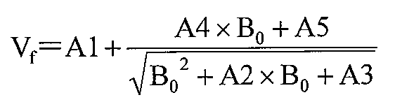
で表され、この式によって得られる出力電圧が前記測定値データにフィッティングするように各係数A1~A5を算出する、前記[5]に記載の電流検出装置(10/10A)。
この電流検出装置(10/10A)は、前記[2]に記載の電流検出方法に対応するものである。
この電流検出装置(10/10A)は、前記[3]に記載の電流検出方法に対応するものである。
この電流検出装置(10/10A)は、前記[4]に記載の電流検出方法に対応するものである。
この電流検出装置(10)の信号補正方法は、磁気検出素子(11,12)と信号補正部(15)とを共に1つのチップ内に収納して構成してある電流検出装置(10)に、所定の磁束密度(B)を供給し、磁束密度(B)と電流検出装置(10)の出力電圧信号(V1)との関係を示す測定値データを取得し、取得した測定値データを用いて所定の式(1)又は式(3)とが互いにフィッティングするように演算処理を施し、係数群(Voff,Vsat,Bb,φ,α/A1~A5)を算出し、算出した係数群に従って、信号補正部(15)を用いて磁気検出素子(11,12)からの出力電圧信号(V1)を磁束密度(B)に対して略線形となるように補正し、その補正電圧信号(VL)を出力するようにしたものである。これによって、検出される磁束密度(B)に対する出力電圧(V1)の関係を直線性の高い略線形とすることが可能となる。
この電流検出装置(10)の信号補正方法は、信号補正部(15)から出力される略直線化補正された出力電圧信号V1が略直線的に変化しているか否か、すなわち略線形か否かの判定を行い、線形である(yes)と判定される場合は、略直線的に変化しているとみなせる被測定磁場の範囲±Bを記憶部(16)に書き込み、線形でない(no)と判定された場合は、測定範囲を限定して、再度フィッティング処理を行うようにしたものである。これによって、補正電圧信号V1は、より高い直線性を示す略線形に近い出力となる。また、被測定磁場の範囲±Bを記憶部(16)に書き込むことによって、記憶部(16)からその範囲±Bを読みだすことで、電流検出装置(10)の測定範囲を容易に確認することができる。
この電流検出装置(10A)の信号補正方法は、電流検出装置10Aとは別のチップ上に収納された信号補正装置15Aを用いて、電流検出装置10Aから出力される出力電圧信号Voutを所定の係数に基づいて略直線的に変化するような補正出力電圧信号VLとして出力するようにしたものであり、その信号補正方法は、前記[9]に記載の方法と同様である。これによって、既に被測定対象物に設置済の電流検出装置や信号補正部を有さない電流検出装置(10A)に対しても、検出される磁束密度(B)に対する出力電圧(V1)の関係を直線性の高い略線形とすることが可能となる。
この電流検出装置(10A)の信号補正方法は、前記[10]に記載の電流検出装置(10)の信号補正方法に対応するものである。

で表され、この式の出力電圧Vfが前記測定値データにフィッティングするように各係数A1~A5を算出する、前記[9]乃至[13]の何れか1項に記載の電流検出装置(10/10A)の信号補正方法。
この電流検出装置(10/10A)の信号補正方法は、前記[2]に記載の電流検出方法に対応するものである。
この電流検出装置(10/10A)の信号補正方法は、前記[3]に記載の電流検出方法に対応するものである。
この電流検出装置(10A)の信号補正装置(15A)は、前記[11]に記載の電流検出装置(10A)の信号補正方法に対応するものである。
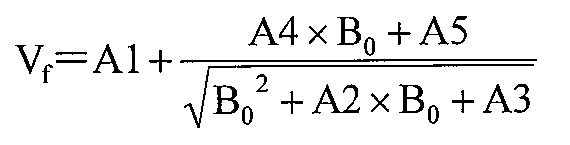
で表され、この式の出力電圧Vfが前記測定値データにフィッティングするように各係数A1~A5を算出する、前記[16]に記載の電流検出装置(10A)の信号補正装置(15A)。
この電流検出装置(10A)の信号補正装置(15A)は、前記[3]に記載の電流検出方法、及び前記[13]に記載の電流検出装置(10A)の信号補正方法に対応するものである。
[19]前記式(1)の出力電圧信号Vfを出力電圧信号V1に置き換え、合成磁界B0を前記出力電圧信号V1の関数(B0(V1))とした場合の次式と、VL=m×B0(V1)+n(この式において、係数mは0以外の任意の値,nは任意の値とする)、前記演算処理によって得られた前記複数の係数群(Voff,Vsat,Bb,φ,α/A1~A5)とに従って、前記補正電圧信号(VL)を出力する、前記[17]又は[18]に記載の電流検出装置(10A)の信号補正装置(15A)。
この電流検出装置(10A)の信号補正装置(15A)は、前記[4]に記載の電流検出方法、及び前記[14]に記載の電流検出装置(10A)の信号補正方法に対応するものである。
Vsat…飽和出力係数
Bb…バイアス磁界強度係数
φ…被測定磁界方向の角度ずれ係数
α…バイアス磁界方向の角度ずれ係数
A1~A5…係数
10,10A…電流検出装置
11,12…磁気検出素子
15…信号補正部
15A…信号補正装置
16,16A…記憶部
20…磁界発生装置
21…磁気シールドボックス
22…ソレノイドコイル
30,30A…制御部
31…被測定磁界用定電流源
32…定電圧源
34,34A…電圧測定部
35,35A…フィッティング係数演算部
36,36A…係数制御部
Claims (19)
- 磁束密度を検出し、前記磁束密度に対応した電圧信号を出力する磁気検出素子を備えた電流検出装置に対して、
前記磁気検出素子が検出可能な範囲の磁束密度を供給することによって得られる、前記磁束密度と前記電流検出装置の出力電圧信号との関係を示す測定値データを取得し、
取得した前記測定値データと、複数の係数群を含んで構成される磁気検出素子の出力電圧を示す式とが互いにフィッティングするように演算処理することによって前記複数の係数群を算出し、
算出された前記複数の係数群に従って、前記磁気検出素子からの出力電圧信号を前記磁束密度に対して略線形となるように補正し、補正された補正電圧信号を出力する、
電流検出方法。 - 複数の係数群を含んで構成される磁気検出素子の出力電圧を示す式は、
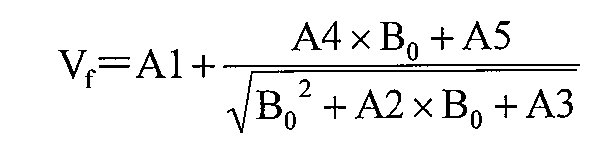
で表され、
この式によって得られる出力電圧が前記測定値データにフィッティングするように各係数A1~A5を算出する、
請求項1に記載の電流検出方法。 - 前記式を構成する係数A1は出力オフセット係数Voff、係数A2は2・Bb・sin(α-φ)、係数A3はBbの二乗、係数A4はVsat・cosφ、係数A5はBb・Vsat・sinαであり、
前記係数A2~A5において、Vsatは飽和出力係数、Bbはバイアス磁界強度係数、φは被測定磁界方向の角度ずれ係数、αはバイアス磁界方向の角度ずれ係数である、
請求項2に記載の電流検出方法。 - 前記式の出力電圧信号Vfを出力電圧信号V1に置き換え、合成磁界B0を前記出力電圧信号V1の関数(B0(V1))とした場合の次式と、
VL=m×B0(V1)+n
(この式において、係数mは0以外の任意の値,nは任意の値とする)、
前記演算処理によって得られた前記複数の係数群とに従って、
前記補正電圧信号を出力する、
請求項2又は3に記載の電流検出方法。 - 磁束密度を検出し、前記磁束密度に対応した電圧信号を出力する磁気検出素子と、
前記磁気検出素子に磁束密度を供給することによって得られる磁束密度と出力電圧信号との関係を示す測定値データと、複数の係数群を含んで構成される磁気検出素子の出力電圧を示す式とが互いにフィッティングするように演算処理することによって得られた前記複数の係数群に従って、前記磁気検出素子からの出力電圧信号を前記磁束密度に対して略線形となるように補正し、補正された補正電圧信号を出力する信号補正手段と、
を備えた電流検出装置。 - 複数の係数群を含んで構成される磁気検出素子の出力電圧を示す式は、
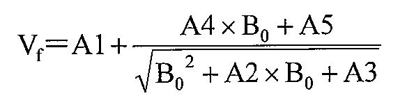
で表され、
この式の出力電圧Vfが前記測定値データにフィッティングするように各係数A1~A5を算出する、
請求項5に記載の電流検出装置。 - 前記式を構成する係数A1は出力オフセット係数Voff、係数A2は2・Bb・sin(α-φ)、係数A3はBbの二乗、係数A4をVsat・cosφ、係数A5はBb・Vsat・sinαであり、
前記係数A2~A5において、Vsatは飽和出力係数、Bbはバイアス磁界強度係数、φは被測定磁界方向の角度ずれ係数、αはバイアス磁界方向の角度ずれ係数である、
請求項6に記載の電流検出装置。 - 前記信号補正手段は、
前記式(1)の出力電圧信号Vfを出力電圧信号V1に置き換え、合成磁界B0を前記出力電圧信号V1の関数(B0(V1))とした場合の次式と、
VL=m×B0(V1)+n・・・(2)
(この式において、係数mは0以外の任意の値,nは任意の値である)、
前記演算処理によって得られた前記複数の係数群とに従って、
前記補正電圧信号を出力する、
請求項6又は7に記載の電流検出装置。 - 磁束密度を検出し、前記磁束密度に対応した電圧信号を出力する磁気検出素子と、複数の係数群を記憶する記憶部を備えており、前記記憶部に前記複数の係数群が記憶されていない場合には、前記磁気検出素子からの出力電圧信号をそのまま出力し、前記記憶部に前記複数の係数群が記憶されている場合には、前記複数の係数群に従って、前記磁気検出素子からの出力電圧信号を前記磁束密度に対して略線形となるように補正し、補正された補正電圧信号を出力する信号補正手段とを備えた電流検出装置であって、前記信号補正手段の前記記憶部に前記複数の係数群が記憶されていない電流検出装置に対して、
前記磁気検出素子が検出可能な範囲の磁束密度を供給し、
それによって得られる前記磁束密度と前記電流検出装置の出力電圧信号との関係を示す測定値データを取得し、
取得した前記測定値データと、複数の係数群を含んで構成される磁気検出素子の出力電圧を示す式とが互いにフィッティングするように演算処理することによって前記複数の係数群を算出し、
算出された前記複数の係数群を前記信号補正手段の前記記憶部に記憶する、
電流検出装置の信号補正方法。 - 前記信号補正手段の前記記憶部に前記複数の係数群を記憶した後に、
前記電流検出装置に対して、前記磁気検出素子が検出可能な範囲の磁束密度を供給することによって得られる前記補正電圧信号を測定し、
測定した前記補正電圧信号が略線形を示すか否かを判定し、
略線形を示す場合は、被測定磁場による測定範囲を前記記憶部に記憶し、
略線形を示さない場合は、被測定磁場の範囲を限定して、前記演算処理を再度実行して前記複数の係数群を算出し、
算出された前記複数の係数群及び前記限定した被測定磁場の範囲を前記信号補正手段の前記記憶部に記憶する、
請求項9に記載の電流検出装置の信号補正方法。 - 磁束密度を検出し、前記磁束密度に対応した電圧信号を出力する磁気検出素子を備えた電流検出装置に対して、
前記磁気検出素子が検出可能な範囲の磁束密度を供給することによって得られる、前記磁束密度と前記電流検出装置の出力電圧信号との関係を示す測定値データを取得し、
取得した前記測定値データと、複数の係数群を含んで構成される磁気検出素子の出力電圧を示す式とが互いにフィッティングするように演算処理することによって前記複数の係数群を算出し、
前記複数の係数群に従って前記磁気検出素子からの出力電圧信号を前記磁束密度に対して略線形となるように補正し、補正された補正電圧信号を出力する信号補正手段の前記記憶部に、算出された前記複数の係数群を記憶し、
前記複数の係数群を前記記憶部に記憶した前記信号補正手段を、前記電流検出装置の信号補正装置として使用する、
電流検出装置の信号補正方法。 - 前記信号補正手段の前記記憶部に前記複数の係数群を記憶した後に、
前記電流検出装置に対して、前記磁気検出素子が検出可能な範囲の磁束密度を供給することによって得られる前記補正電圧信号を測定し、
測定した前記補正電圧信号が略線形を示すか否かを判定し、
略線形を示す場合は、被測定磁場による測定範囲を前記記憶部に記憶し、
略線形を示さない場合は、被測定磁場の範囲を限定して、前記演算処理を再度実行して前記複数の係数群を算出し、
算出された前記複数の係数群及び前記限定した被測定磁場の範囲を前記信号補正手段の前記記憶部に記憶し、
前記複数の係数群及び前記限定した被測定磁場の範囲を前記記憶部に記憶した前記信号補正手段を、前記電流検出装置の信号補正装置として使用する、
請求項11に記載の電流検出装置の信号補正方法。 - 複数の係数群を含んで構成される磁気検出素子の出力電圧を示す式は、

で表され、
この式の出力電圧Vfが前記測定値データにフィッティングするように各係数A1~A5を算出する、
請求項9乃至12の何れか1項に記載の電流検出装置の信号補正方法。 - 前記式を構成する係数A1は出力オフセット係数Voff、係数A2は2・Bb・sin(α-φ)、係数A3はBbの二乗、係数A4をVsat・cosφ、係数A5はBb・Vsat・sinαであり、
前記係数A2~A5において、Vsatは飽和出力係数、Bbはバイアス磁界強度係数、φは被測定磁界方向の角度ずれ係数、αはバイアス磁界方向の角度ずれ係数である、
請求項13に記載の電流検出装置の信号補正方法。 - 前記電流検出装置の前記信号補正手段は、
前記式の出力電圧Vfを出力電圧V1に置き換え、合成磁界B0を前記出力電圧V1の関数(B0(V1))とした場合の次式と、
VL=m×B0(V1)+n
(この式において、係数mは0以外の任意の値、nは任意の値とする)、
前記演算処理によって算出された前記複数の係数群とに従って、
前記補正電圧信号を出力する、
請求項13又は14に記載の電流検出装置の信号補正方法。 - 磁束密度を検出し、前記磁束密度に対応した電圧信号を出力する磁気検出素子を備えた電流検出装置に接続され、前記出力電圧信号を補正して出力する電流検出装置の信号補正装置であって、
前記磁気検出素子に磁束密度を供給することによって得られる磁束密度と出力電圧信号との関係を示す測定値データと、複数の係数群を含んで構成される磁気検出素子の出力電圧を示す式とが互いにフィッティングするように演算処理することによって得られた前記複数の係数群に従って、前記磁気検出素子からの出力電圧信号を前記磁束密度に対して略線形となるように補正し、補正された補正電圧信号を出力する、
電流検出装置の信号補正装置。 - 複数の係数群を含んで構成される磁気検出素子の出力電圧を示す式は、
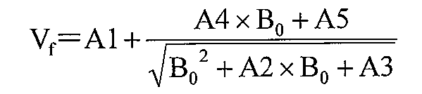
で表され、
この式の出力電圧Vfが前記測定値データにフィッティングするように各係数A1~A5を算出する、
請求項16に記載の電流検出装置の信号補正装置。 - 前記式を構成する係数A1は出力オフセット係数Voff、係数A2は2・Bb・sin(α-φ)、係数A3はBbの二乗、係数A4はVsat・cosφ、係数A5はBb・Vsat・sinαであり、
前記係数A2~A5において、Vsatは飽和出力係数、Bbはバイアス磁界強度係数、φは被測定磁界方向の角度ずれ係数、αはバイアス磁界方向の角度ずれ係数である、
請求項17に記載の電流検出装置の信号補正装置。 - 前記電流検出装置の前記信号補正手段は、
前記式の出力電圧Vfを出力電圧V1に置き換え、合成磁界B0を前記出力電圧V1の関数(B0(V1))とした場合の次式と、
VL=m×B0(V1)+n
(この式において、係数mは0以外の任意の値、nは任意の値とする)、
前記演算処理によって算出された前記複数の係数群とに従って、
前記補正電圧信号を出力する、
請求項17又は18に記載の電流検出装置の信号補正装置。
Priority Applications (4)
| Application Number | Priority Date | Filing Date | Title |
|---|---|---|---|
| CN201480082608.1A CN107076783B (zh) | 2014-10-10 | 2014-10-10 | 电流检测方法、电流检测装置、电流检测装置的信号修正方法、以及电流检测装置的信号修正装置 |
| JP2016552792A JP6477718B2 (ja) | 2014-10-10 | 2014-10-10 | 電流検出方法、電流検出装置、電流検出装置の信号補正方法、及び電流検出装置の信号補正装置 |
| PCT/JP2014/077246 WO2016056136A1 (ja) | 2014-10-10 | 2014-10-10 | 電流検出方法、電流検出装置、電流検出装置の信号補正方法、及び電流検出装置の信号補正装置 |
| US15/517,614 US10996246B2 (en) | 2014-10-10 | 2014-10-10 | Current detection method, current detection device, signal correction method for current detection device, and signal correction device for current detection device |
Applications Claiming Priority (1)
| Application Number | Priority Date | Filing Date | Title |
|---|---|---|---|
| PCT/JP2014/077246 WO2016056136A1 (ja) | 2014-10-10 | 2014-10-10 | 電流検出方法、電流検出装置、電流検出装置の信号補正方法、及び電流検出装置の信号補正装置 |
Publications (1)
| Publication Number | Publication Date |
|---|---|
| WO2016056136A1 true WO2016056136A1 (ja) | 2016-04-14 |
Family
ID=55652788
Family Applications (1)
| Application Number | Title | Priority Date | Filing Date |
|---|---|---|---|
| PCT/JP2014/077246 Ceased WO2016056136A1 (ja) | 2014-10-10 | 2014-10-10 | 電流検出方法、電流検出装置、電流検出装置の信号補正方法、及び電流検出装置の信号補正装置 |
Country Status (4)
| Country | Link |
|---|---|
| US (1) | US10996246B2 (ja) |
| JP (1) | JP6477718B2 (ja) |
| CN (1) | CN107076783B (ja) |
| WO (1) | WO2016056136A1 (ja) |
Cited By (4)
| Publication number | Priority date | Publication date | Assignee | Title |
|---|---|---|---|---|
| JP2018115928A (ja) * | 2017-01-17 | 2018-07-26 | 日立金属株式会社 | 電流センサの信号補正方法、及び電流センサ |
| JP2018115929A (ja) * | 2017-01-17 | 2018-07-26 | 日立金属株式会社 | 電流センサの信号補正方法、及び電流センサ |
| KR20230170901A (ko) * | 2020-12-30 | 2023-12-19 | 크로커스 테크놀로지 인코포레이티드 | 고차 전압 출력 부품의 연속 보정에 기반한 자기 센서출력의 선형화 |
| JP2025144347A (ja) * | 2024-03-19 | 2025-10-02 | Tdk株式会社 | 磁気センサ装置、磁気センサシステムおよび補正方法 |
Families Citing this family (2)
| Publication number | Priority date | Publication date | Assignee | Title |
|---|---|---|---|---|
| CN113809972B (zh) * | 2021-10-25 | 2023-12-15 | 国华(青岛)智能装备有限公司 | 一种机器人用电机的位置传感器误差矫正系统及控制方法 |
| WO2024062401A1 (en) * | 2022-09-21 | 2024-03-28 | Basis NZ Limited | Current detection device and related devices, systems and methods thereof |
Citations (2)
| Publication number | Priority date | Publication date | Assignee | Title |
|---|---|---|---|---|
| JP2001343439A (ja) * | 2000-06-05 | 2001-12-14 | Tokin Corp | 高周波キャリア型磁気センサ |
| JP2008203238A (ja) * | 2007-02-21 | 2008-09-04 | Koshin Denki Kk | 電流検知デバイス |
Family Cites Families (12)
| Publication number | Priority date | Publication date | Assignee | Title |
|---|---|---|---|---|
| JPS599865B2 (ja) * | 1975-04-07 | 1984-03-05 | 株式会社リコー | 磁界測定方法 |
| JPH09329628A (ja) * | 1996-06-06 | 1997-12-22 | Toyo Commun Equip Co Ltd | ホール素子式電流検出器 |
| JP2000055997A (ja) | 1998-08-05 | 2000-02-25 | Tdk Corp | 磁気センサ装置および電流センサ装置 |
| US6633462B2 (en) * | 2000-07-13 | 2003-10-14 | Koninklijke Philips Electronics N.V. | Magnetoresistive angle sensor having several sensing elements |
| JP2002156390A (ja) * | 2000-11-21 | 2002-05-31 | Na:Kk | 電流センサ |
| JP4049125B2 (ja) * | 2004-05-20 | 2008-02-20 | コニカミノルタオプト株式会社 | 位置検出装置、手振れ補正機構、および撮像装置 |
| CN101065682A (zh) * | 2004-11-25 | 2007-10-31 | 皇家飞利浦电子股份有限公司 | 具有并联的磁传感器条的磁传感器 |
| HUE027441T2 (en) * | 2004-12-17 | 2016-10-28 | Hitachi Metals Ltd | Magnetic core for power transformer, current transformer and watt meter |
| JP2006266909A (ja) * | 2005-03-24 | 2006-10-05 | Alps Electric Co Ltd | 磁気検出装置及びそれを用いた電子方位計 |
| JP4165589B2 (ja) * | 2006-08-09 | 2008-10-15 | ソニー株式会社 | 検出装置およびその検出方法 |
| CN101634666B (zh) * | 2009-06-26 | 2011-09-07 | 祝波 | 一种超大电流霍尔检测方法及装置 |
| CN103575960B (zh) * | 2013-10-29 | 2016-03-02 | 河北工业大学 | 巨磁阻效应电流传感器 |
-
2014
- 2014-10-10 WO PCT/JP2014/077246 patent/WO2016056136A1/ja not_active Ceased
- 2014-10-10 US US15/517,614 patent/US10996246B2/en not_active Expired - Fee Related
- 2014-10-10 CN CN201480082608.1A patent/CN107076783B/zh not_active Expired - Fee Related
- 2014-10-10 JP JP2016552792A patent/JP6477718B2/ja not_active Expired - Fee Related
Patent Citations (2)
| Publication number | Priority date | Publication date | Assignee | Title |
|---|---|---|---|---|
| JP2001343439A (ja) * | 2000-06-05 | 2001-12-14 | Tokin Corp | 高周波キャリア型磁気センサ |
| JP2008203238A (ja) * | 2007-02-21 | 2008-09-04 | Koshin Denki Kk | 電流検知デバイス |
Cited By (7)
| Publication number | Priority date | Publication date | Assignee | Title |
|---|---|---|---|---|
| JP2018115928A (ja) * | 2017-01-17 | 2018-07-26 | 日立金属株式会社 | 電流センサの信号補正方法、及び電流センサ |
| JP2018115929A (ja) * | 2017-01-17 | 2018-07-26 | 日立金属株式会社 | 電流センサの信号補正方法、及び電流センサ |
| KR20230170901A (ko) * | 2020-12-30 | 2023-12-19 | 크로커스 테크놀로지 인코포레이티드 | 고차 전압 출력 부품의 연속 보정에 기반한 자기 센서출력의 선형화 |
| JP2024503359A (ja) * | 2020-12-30 | 2024-01-25 | クロッカス・テクノロジー・インコーポレイティド | 高次電圧出力成分の連続補正に基づく磁気センサ出力の線形化 |
| KR102945513B1 (ko) | 2020-12-30 | 2026-03-30 | 알레그로 마이크로시스템스, 엘엘씨 | 고차 전압 출력 부품의 연속 보정에 기반한 자기 센서 출력의 선형화 |
| JP2025144347A (ja) * | 2024-03-19 | 2025-10-02 | Tdk株式会社 | 磁気センサ装置、磁気センサシステムおよび補正方法 |
| JP7813309B2 (ja) | 2024-03-19 | 2026-02-12 | Tdk株式会社 | 磁気センサ装置、磁気センサシステムおよび補正方法 |
Also Published As
| Publication number | Publication date |
|---|---|
| US20170307663A1 (en) | 2017-10-26 |
| CN107076783B (zh) | 2019-11-05 |
| JP6477718B2 (ja) | 2019-03-06 |
| JPWO2016056136A1 (ja) | 2017-07-20 |
| CN107076783A (zh) | 2017-08-18 |
| US10996246B2 (en) | 2021-05-04 |
Similar Documents
| Publication | Publication Date | Title |
|---|---|---|
| US11199424B2 (en) | Reducing angle error in a magnetic field angle sensor | |
| JP7006633B2 (ja) | 磁気センサシステム | |
| JP6477718B2 (ja) | 電流検出方法、電流検出装置、電流検出装置の信号補正方法、及び電流検出装置の信号補正装置 | |
| US10648787B2 (en) | Rotating field sensor | |
| US9429632B2 (en) | Magnetic position detection device | |
| EP2284555B1 (en) | Magnetic sensor including a bridge circuit | |
| JP6323699B1 (ja) | 角度センサおよび角度センサシステム | |
| US10557726B2 (en) | Systems and methods for reducing angle error for magnetic field angle sensors | |
| US20160169707A1 (en) | Rotating field sensor | |
| JP2016166741A (ja) | 磁気センサ | |
| CN105629023A (zh) | 电流检测装置 | |
| JP2018115929A (ja) | 電流センサの信号補正方法、及び電流センサ | |
| US11313666B2 (en) | Angle sensor and angle sensor system | |
| JP6947194B2 (ja) | 信号処理回路および磁気センサシステム | |
| JP7156249B2 (ja) | 位置検出装置 | |
| JP6897106B2 (ja) | 電流センサの信号補正方法、及び電流センサ | |
| US20260056267A1 (en) | Magnetic sensor, electric control device, and correction method | |
| US20200025551A1 (en) | Correction apparatus for angle sensor, and angle sensor | |
| US20200333408A1 (en) | Magnetoresistive Magnetic Field Sensor Bridge with Compensated Cross-Axis Effect | |
| JP6378338B2 (ja) | 磁気センサ | |
| CN108469594A (zh) | 一种高精度、闭环式梯度磁阻传感器 |
Legal Events
| Date | Code | Title | Description |
|---|---|---|---|
| 121 | Ep: the epo has been informed by wipo that ep was designated in this application |
Ref document number: 14903711 Country of ref document: EP Kind code of ref document: A1 |
|
| ENP | Entry into the national phase |
Ref document number: 2016552792 Country of ref document: JP Kind code of ref document: A |
|
| WWE | Wipo information: entry into national phase |
Ref document number: 15517614 Country of ref document: US |
|
| NENP | Non-entry into the national phase |
Ref country code: DE |
|
| 122 | Ep: pct application non-entry in european phase |
Ref document number: 14903711 Country of ref document: EP Kind code of ref document: A1 |