WO2016017352A1 - Led実装用基板、led - Google Patents
Led実装用基板、led Download PDFInfo
- Publication number
- WO2016017352A1 WO2016017352A1 PCT/JP2015/068945 JP2015068945W WO2016017352A1 WO 2016017352 A1 WO2016017352 A1 WO 2016017352A1 JP 2015068945 W JP2015068945 W JP 2015068945W WO 2016017352 A1 WO2016017352 A1 WO 2016017352A1
- Authority
- WO
- WIPO (PCT)
- Prior art keywords
- pad
- led
- terminal
- irregularly shaped
- shape
- Prior art date
Links
Images


Classifications
-
- H—ELECTRICITY
- H01—ELECTRIC ELEMENTS
- H01L—SEMICONDUCTOR DEVICES NOT COVERED BY CLASS H10
- H01L33/00—Semiconductor devices with at least one potential-jump barrier or surface barrier specially adapted for light emission; Processes or apparatus specially adapted for the manufacture or treatment thereof or of parts thereof; Details thereof
- H01L33/48—Semiconductor devices with at least one potential-jump barrier or surface barrier specially adapted for light emission; Processes or apparatus specially adapted for the manufacture or treatment thereof or of parts thereof; Details thereof characterised by the semiconductor body packages
- H01L33/62—Arrangements for conducting electric current to or from the semiconductor body, e.g. lead-frames, wire-bonds or solder balls
-
- H—ELECTRICITY
- H01—ELECTRIC ELEMENTS
- H01L—SEMICONDUCTOR DEVICES NOT COVERED BY CLASS H10
- H01L33/00—Semiconductor devices with at least one potential-jump barrier or surface barrier specially adapted for light emission; Processes or apparatus specially adapted for the manufacture or treatment thereof or of parts thereof; Details thereof
- H01L33/48—Semiconductor devices with at least one potential-jump barrier or surface barrier specially adapted for light emission; Processes or apparatus specially adapted for the manufacture or treatment thereof or of parts thereof; Details thereof characterised by the semiconductor body packages
- H01L33/483—Containers
- H01L33/486—Containers adapted for surface mounting
-
- H—ELECTRICITY
- H05—ELECTRIC TECHNIQUES NOT OTHERWISE PROVIDED FOR
- H05K—PRINTED CIRCUITS; CASINGS OR CONSTRUCTIONAL DETAILS OF ELECTRIC APPARATUS; MANUFACTURE OF ASSEMBLAGES OF ELECTRICAL COMPONENTS
- H05K1/00—Printed circuits
- H05K1/02—Details
- H05K1/11—Printed elements for providing electric connections to or between printed circuits
- H05K1/111—Pads for surface mounting, e.g. lay-out
-
- H—ELECTRICITY
- H05—ELECTRIC TECHNIQUES NOT OTHERWISE PROVIDED FOR
- H05K—PRINTED CIRCUITS; CASINGS OR CONSTRUCTIONAL DETAILS OF ELECTRIC APPARATUS; MANUFACTURE OF ASSEMBLAGES OF ELECTRICAL COMPONENTS
- H05K3/00—Apparatus or processes for manufacturing printed circuits
- H05K3/30—Assembling printed circuits with electric components, e.g. with resistor
- H05K3/32—Assembling printed circuits with electric components, e.g. with resistor electrically connecting electric components or wires to printed circuits
- H05K3/34—Assembling printed circuits with electric components, e.g. with resistor electrically connecting electric components or wires to printed circuits by soldering
- H05K3/341—Surface mounted components
- H05K3/3431—Leadless components
-
- H—ELECTRICITY
- H01—ELECTRIC ELEMENTS
- H01L—SEMICONDUCTOR DEVICES NOT COVERED BY CLASS H10
- H01L33/00—Semiconductor devices with at least one potential-jump barrier or surface barrier specially adapted for light emission; Processes or apparatus specially adapted for the manufacture or treatment thereof or of parts thereof; Details thereof
- H01L33/48—Semiconductor devices with at least one potential-jump barrier or surface barrier specially adapted for light emission; Processes or apparatus specially adapted for the manufacture or treatment thereof or of parts thereof; Details thereof characterised by the semiconductor body packages
- H01L33/64—Heat extraction or cooling elements
-
- H—ELECTRICITY
- H05—ELECTRIC TECHNIQUES NOT OTHERWISE PROVIDED FOR
- H05K—PRINTED CIRCUITS; CASINGS OR CONSTRUCTIONAL DETAILS OF ELECTRIC APPARATUS; MANUFACTURE OF ASSEMBLAGES OF ELECTRICAL COMPONENTS
- H05K2201/00—Indexing scheme relating to printed circuits covered by H05K1/00
- H05K2201/09—Shape and layout
- H05K2201/09209—Shape and layout details of conductors
- H05K2201/09372—Pads and lands
- H05K2201/09381—Shape of non-curved single flat metallic pad, land or exposed part thereof; Shape of electrode of leadless component
-
- H—ELECTRICITY
- H05—ELECTRIC TECHNIQUES NOT OTHERWISE PROVIDED FOR
- H05K—PRINTED CIRCUITS; CASINGS OR CONSTRUCTIONAL DETAILS OF ELECTRIC APPARATUS; MANUFACTURE OF ASSEMBLAGES OF ELECTRICAL COMPONENTS
- H05K2201/00—Indexing scheme relating to printed circuits covered by H05K1/00
- H05K2201/10—Details of components or other objects attached to or integrated in a printed circuit board
- H05K2201/10007—Types of components
- H05K2201/10106—Light emitting diode [LED]
-
- H—ELECTRICITY
- H05—ELECTRIC TECHNIQUES NOT OTHERWISE PROVIDED FOR
- H05K—PRINTED CIRCUITS; CASINGS OR CONSTRUCTIONAL DETAILS OF ELECTRIC APPARATUS; MANUFACTURE OF ASSEMBLAGES OF ELECTRICAL COMPONENTS
- H05K2201/00—Indexing scheme relating to printed circuits covered by H05K1/00
- H05K2201/10—Details of components or other objects attached to or integrated in a printed circuit board
- H05K2201/10613—Details of electrical connections of non-printed components, e.g. special leads
- H05K2201/10954—Other details of electrical connections
- H05K2201/10969—Metallic case or integral heatsink of component electrically connected to a pad on PCB
-
- H—ELECTRICITY
- H05—ELECTRIC TECHNIQUES NOT OTHERWISE PROVIDED FOR
- H05K—PRINTED CIRCUITS; CASINGS OR CONSTRUCTIONAL DETAILS OF ELECTRIC APPARATUS; MANUFACTURE OF ASSEMBLAGES OF ELECTRICAL COMPONENTS
- H05K2203/00—Indexing scheme relating to apparatus or processes for manufacturing printed circuits covered by H05K3/00
- H05K2203/04—Soldering or other types of metallurgic bonding
- H05K2203/048—Self-alignment during soldering; Terminals, pads or shape of solder adapted therefor
-
- Y—GENERAL TAGGING OF NEW TECHNOLOGICAL DEVELOPMENTS; GENERAL TAGGING OF CROSS-SECTIONAL TECHNOLOGIES SPANNING OVER SEVERAL SECTIONS OF THE IPC; TECHNICAL SUBJECTS COVERED BY FORMER USPC CROSS-REFERENCE ART COLLECTIONS [XRACs] AND DIGESTS
- Y02—TECHNOLOGIES OR APPLICATIONS FOR MITIGATION OR ADAPTATION AGAINST CLIMATE CHANGE
- Y02P—CLIMATE CHANGE MITIGATION TECHNOLOGIES IN THE PRODUCTION OR PROCESSING OF GOODS
- Y02P70/00—Climate change mitigation technologies in the production process for final industrial or consumer products
- Y02P70/50—Manufacturing or production processes characterised by the final manufactured product
Definitions
- the present invention relates to an LED mounting substrate and an LED on which the mounting type LED is mounted.
- the surface-mount type electronic component is placed on a pad to which cream solder or the like is applied in advance, and is mounted on the substrate by soldering by reflow, for example.
- the pad and the terminal joint surface of the electronic component are slightly different in size (in the specification, it is recommended to design the pad larger than the terminal joint surface of the electronic component), and as a result, In the reflow process, when the solder is melted, the electronic component may move on the pad, resulting in unexpected displacement.
- the shape of the pad (metallized layer) is different from the terminal shape, so that only a part of the pad and the terminal joint surface of the electronic component are superposed. With this configuration, the electronic component is prevented from being displaced using the surface tension of the solder.
- such a misregistration prevention mechanism has an advantage that the optical axes are accurately aligned when the electronic component is an LED, but may have a problem in terms of heat dissipation. That is, in the case of an LED in which heat dissipation is particularly important, there may be a problem that the pad's heat dissipation function cannot be sufficiently exerted if the pad and the terminal joint surface are partially overlapped.
- the present invention has been made in view of such problems, and is intended to easily prevent misalignment during soldering of a surface-mounted LED without impairing the heat dissipation function.
- the LED mounting substrate according to the present invention is mounted with a surface-mounted LED having a plurality of terminals, and includes a plurality of pads to which the terminals are soldered, and has a heat dissipation function.
- At least one pad hereinafter referred to as “unshaped pad”) excluding the highest pad (hereinafter referred to as “heat dissipating pad”) has a shape different from the shape of the corresponding terminal, and the LED is mounted.
- a terminal corresponding to the irregularly shaped pad and the irregularly shaped pad have a non-polymerized part, and the non-polymerized part is a surface of the molten solder only in a regular position where the LED is mounted. It is characterized in that the resultant force of the force acting on the boundary between the portions where the pad and the terminal overlap is balanced by tension.
- the LED can be surely arranged at a normal position through a soldering process, and positional deviation can be prevented.
- pads other than the heat dissipating pads are provided in different shapes, it is possible to prevent the formation of non-polymerized portions between the heat dissipating pads and the corresponding terminals, and to prevent the heat dissipation from being impaired. it can.
- the “unshaped pad” includes a terminal having a shape different from that of the terminal and a similar shape having the same shape as the terminal but having a different size.
- the LED when the LED is mounted at a predetermined regular position, if it is configured so that substantially the entire terminal joint surface corresponding to the heat dissipating pad is placed on the heat dissipating pad, the heat dissipating at the normal position is provided. Since almost the entire joining surface of the terminal is superposed on the heat dissipating pad, an important heat dissipating function can be secured when the LED is mounted.
- this type of surface-mount type LED has a bottomed groove that is cut off from the back surface on the side end surface of the package.
- the bottomed groove is configured such that a part of the terminal attached to the back surface of the package extends, and the solder goes up to the side peripheral surface of the package through the extended portion.
- the present invention is applied to an LED including an LED chip, a package on which the LED chip is mounted, and a plurality of rectangular terminals formed on the back surface of the package,
- the pad has a generally rectangular shape arranged side by side corresponding to the terminal, and the irregularly shaped pad has a shape in which a notch is provided in a corner or side on the adjacent pad side. Can be mentioned.
- Specific embodiments capable of maintaining good solderability include an LED chip, a package on which the LED chip is mounted, and a plurality of rectangular terminals formed on the back surface of the package, and a part of the terminals Is applied to an LED configured to form a stretched portion extending to the side end surface of the package, and the pad has a substantially rectangular shape arranged side by side corresponding to the terminal, Among them, the irregularly shaped pad has a shape in which a notch is provided at one corner or side, and the notch is provided so as to avoid the extending portion.
- the corner angle of the irregularly shaped pad can be avoided. Are all set to 90 degrees or more.
- the LED according to the present invention is a surface-mounted LED mounted on an LED mounting substrate having a plurality of pads including a pad having the highest heat dissipation function (hereinafter referred to as “heat dissipation pad”). And at least one terminal excluding the terminal corresponding to the heat dissipating pad (hereinafter referred to as “unshaped terminal”) has a shape different from the shape of the corresponding pad.
- the pad corresponding to the irregularly shaped terminal and the irregularly shaped terminal do not overlap with each other at the regular position where the LED is mounted, and the nonpolymerized part is a regular where the LED is mounted. Only at the position, it is provided so that the resultant force of the force acting on the boundary between the portions where the pad and the terminal overlap is balanced by the surface tension of the molten solder. And wherein the door.
- the terminal side rather than the pad side
- the pad side is configured to have a different shape
- the LED when the LED is placed on the substrate with a certain degree of deviation from the normal position, for example, the differential force is balanced only at the normal position. Since the shape terminal is provided, when the solder is melted in the reflow process, the LED moves toward the normal position due to the surface tension of the molten solder, and the LED stops moving at the normal position where the resultant force is balanced. Therefore, the LED can be surely arranged at the normal position, and positional deviation can be prevented.
- terminals other than the terminals corresponding to the heat dissipating pads are provided in different shapes, the formation of non-polymerized portions between the heat dissipating pads and the corresponding terminals is prevented, and heat dissipation is impaired. Can be prevented.
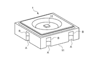
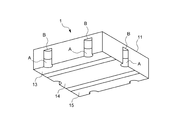
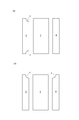
- the perspective view seen from the upper part of LED in one embodiment of the present invention The perspective view seen from the downward direction of LED in the embodiment.
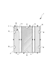
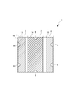
- the top view which shows balance of force when it positions in FIG. The top view which shows the pad in other embodiment of this invention.
- the positioning process figure of LED which shows a movement until LED is positioned in other embodiment of this invention.
- An LED mounting substrate 100 (hereinafter also referred to as “substrate 100”) according to the present embodiment is a pad 2 for soldering terminals 13, 14, and 15 of a surface-mounted LED 1 (hereinafter also referred to as “LED1”).
- Reference numerals 3, 4 denote printed wiring boards formed on the surface thereof. Prior to the description of the substrate 100, the outline of the LED 1 mounted on the substrate 100 will be described first.
- the LED 1 is a surface-mounted type having a flat plate rectangular shape (here, a square shape), and a package 11 having a flat plate square shape and an opening on the surface side of the package 11.
- the LED chip 12 is bonded to the center of the bottomed circular hole, and a plurality (here, three) of terminals 13, 14, and 15 are formed on the back surface of the package 11 by gold plating.
- Terminals 13, 14, and 15 are arranged in a horizontal line with a gap of a constant width, and have a substantially rectangular shape with the same vertical dimension but different horizontal dimensions.
- the direction in which the terminals 13, 14, and 15 are arranged is referred to as a horizontal direction, and the direction orthogonal thereto is referred to as a vertical direction.
- terminals 13 and 15 at both ends having a narrow width (lateral dimension) are electrode (anode and cathode) terminals, respectively, and a central terminal 14 having a wide width and the largest area is a heat sink.
- Terminal Each of these terminals 13, 14, 15 is extended not only to the back surface but also to each side end face of the package 11.
- the extending portion A in which the terminals 13, 14, 15 are extended to the side end surface in this way is that the solder goes up to the side end surface of the package 11 through the extending portion A, so that a so-called fillet is formed. In this way, the holding power is increased.
- a bottomed groove B extending from the back surface to the front surface is provided on each side end surface of the package 11, and the extending portion A by gold plating is formed on the bottom surface of the bottomed groove B.
- the bottomed groove B is used for the purpose of allowing excess solder to escape into the bottomed groove B.
- Two bottomed grooves B are provided on each side end surface parallel to the longitudinal direction of the package 11, and extending portions A of the electrode terminals 13 and 15 are formed there.
- one bottomed groove B is provided on each side end surface parallel to the lateral direction of the package 11, and an extending portion A of the heat radiation terminal 14 is formed.
- the substrate 100 is provided with pads 2, 3, 4 at positions corresponding to the terminals 13, 14, 15 of the LED 1 (see FIG. 3).
- Pads 2 and 4 (hereinafter also referred to as electrode pads 2 and 4) corresponding to the electrode terminals 13 and 15 on both sides have a narrow rectangular shape, respectively, and the lateral dimension X1 thereof is
- the vertical dimension Y1 is substantially the same or larger than the maximum allowable lateral dimension
- the vertical dimension Y1 is substantially the same or larger than the maximum allowable vertical dimension of the electrode terminals 13 and 15.
- the pad 3 (hereinafter also referred to as the heat dissipating pad 3) corresponding to the center heat dissipating terminal 14 has a wide rectangular shape, and both the horizontal dimension X3 and the vertical dimension Y3 are the maximum allowable of the heat dissipating terminal 14.
- one electrode pad 2 (hereinafter also referred to as the irregularly shaped pad 2) is cut out obliquely by cutting one corner out of the two inner corners, thereby forming a notch C.
- the irregularly shaped pad 2 is formed into a pentagonal shape.
- the resultant force of these LEDs causes the LED 1 to move in the corner direction (downward on the page) facing the notch C, and the LED 1 moves at a position where the resultant force balances. Stops.
- the position where the resultant force is balanced is the normal position.
- FIG. 5 is an enlarged view of the irregularly shaped pad 2 and the terminal 13 shown in FIG.
- the side of the terminal 13 corresponding to the side in the lateral direction where the notch C of the irregularly shaped pad 2 is provided is Z1
- the side in the lateral direction opposite to the side Z1 is Z2
- the side of the terminal 13 corresponding to the vertical side where the notch C of the pad 2 is provided is Z3, the vertical side opposite to the side Z3 is Z4, and the vertical direction of the pad 2 having the notch C of the irregularly shaped pad 2 is provided.
- the portion of the terminal 13 that overlaps the side is designated as Z11.
- a force due to the surface tension of the molten solder also acts on the portion of the terminal 13 that overlaps the oblique side forming the notch C of the irregularly shaped pad 2, and this force is perpendicular to the side forming the notch C.
- LED1 moves toward the position where the force mentioned above balances, ie, a normal position.
- the portion forming the notch C becomes a non-polymerized portion 16 where the terminal 13 and the irregularly shaped pad 2 do not overlap, and the terminal 13 protrudes from the irregularly shaped pad 2.
- the LED 1 is positioned in the normal position.
- the regular position in the present embodiment is a position where the sides Z2 and Z4 of the terminal 13 and the corresponding sides of the irregularly shaped pad 2 are exactly overlapped or slightly protruded. At this position, since the surface tension is weakened, the force acting on the side is also weakened.
- the LED 1 is placed in the normal position by the mechanism in which the terminal 13 and the irregularly shaped pad 2 do not overlap at the normal position and the non-polymerized portion 16 provided so as to balance the resultant force due to the surface tension of the molten solder is provided.
- the LED 1 can be positioned by being moved to the position, and the resultant force is balanced at the normal position, so that the positional deviation of the LED 1 can be prevented.
- the notch C for preventing misalignment or positioning is provided only in the electrode pad 2 and not in the heat dissipating pad 3, so that the heat dissipating pad 3 is substantially the joining surface of the heat dissipating terminal 14. The entire surface comes into contact with the solder, and the heat dissipation performance can be reliably ensured.
- the notch C is provided at the inner corner of the irregularly shaped pad 2, that is, the adjacent heat dissipating pad 3 side, the extending portion provided in the bottomed groove B without interfering with the bottomed groove B The formation of fillet by A and the function of sucking off excess solder are not hindered.
- the irregularly shaped pad 2 has an acute angle portion, it is easy for the solder to accumulate therein, and the molten solder overflows from there, for example, reaches the adjacent heat dissipating pad 3 and may cause a short circuit. Since the corner angles of the irregularly shaped pads 2 are all 90 degrees or more and there are no sharp corners, it is possible to prevent problems such as a short circuit due to solder overflow.
- the present invention is not limited to the above embodiment.
- a notch C may be provided at the outer corner of the electrode pad 2. In this case, it is more preferable that the notch C does not reach the extending portion A of the bottomed groove B.
- the shape of the notch C is not limited to a triangle, and may be a partial arc shape, a partial ellipse shape, or an indefinite shape including a plurality of curves and straight lines.
- the corners of the irregularly shaped pad 2 and the terminal 13 are positioned so as to coincide with each other.
- the center lines of the pad 2 and the terminal 13 are aligned with each other. May be.
- FIG. 8A if the notches C are provided symmetrically at both inner corners of the pad 2 and the shape of the notches C is made to be a partial circle, positioning is performed with respect to the center in the vertical direction. Is possible.
- the number of irregularly shaped pads is not limited to one and may be two.
- the electrode pads 2 and 4 may be provided with notches C symmetrically, and these may be formed into irregularly shaped pads. In this way, it is possible to position with reference to the center in the horizontal direction.
- the irregularly shaped pads 2, 4 form a substantially triangular shape arranged so as to be symmetric with respect to the heat radiating pad 3, and specifically, one interior angle of three vertices.
- Forms an obtuse angle isosceles triangle in which the obtuse angle of 90 degrees or more and the two sides sandwiching the apex forming the obtuse angle have the same length.
- the apexes forming the obtuse angles of the irregularly shaped pads 2 and 4 are both directed in the direction in which the heat dissipating pads 3 are arranged.
- the non-polymerized portions 16A where the irregularly shaped pads 2, 4 and the terminals 13, 15 do not overlap each other fix the lateral movement of the LED 1.
- the semicircular bottomed groove B portion fixes the movement of the LED 1 in the vertical direction, so that the LED 1 can be positioned with respect to the vertical center and the horizontal center.
- the present invention is also applicable to a two-terminal LED having only electrode terminals.
- the notch is a terminal having a lower heat dissipation function, that is, a joint surface. It is preferable to provide a small terminal.
- the notch may be provided in the heat-radiating pad.
- the irregularly shaped pad may have a shape that is not generally called a shape with a notch.
- the non-polymerized part where the terminal and the pad do not overlap at the regular position is provided, and the LED is fixed at the regular position. What is necessary is just to be comprised so that it may be made. As a result, the position of the LED is uniquely determined when the solder is melted, and an unexpected position shift can be prevented.
- the pad side is provided in an irregular shape, but the terminal side may be provided in an irregular shape.
- the surface-mounted LED mounted on the surface-mounting substrate having a plurality of pads has a plurality of terminals soldered to the respective pads and has the highest heat radiation function (hereinafter referred to as “heat radiation performance”).
- heat radiation performance the highest heat radiation function
- at least one terminal hereinafter referred to as “different shape terminal” excluding the terminal corresponding to “pad” has a shape different from the shape of the corresponding pad.
- the main problem is to provide an LED mounting substrate that can easily prevent misalignment during soldering of a surface-mounted LED without impairing the heat dissipation function.
Abstract
Description
また、放熱性パッド以外のパッドを異形状に設けたので、放熱性パッドとこれに対応する端子との間に非重合部分が形成されることを防ぎ、放熱性が損なわれることを防ぐことができる。
なお、本発明における「異形状パッド」とは、端子と形状そのものが異なるものや、端子と形状は同じであるがその大きさが異なる相似形のものも含む。
また、放熱性パッドに対応する端子以外の端子を異形状に設けたので、放熱性パッドとこれに対応する端子との間に非重合部分が形成されることを防ぎ、放熱性が損なわれることを防ぐことができる。
2・・・異形状パッド
3・・・放熱性パッド
4・・・電極用パッド
16・・・非重合部分
この基板100の説明に先立って、まずは本基板100に実装されるLED1の概要を説明する。
一方、中央の放熱用端子14に対応するパッド3(以下、放熱性パッド3ともいう。)は広幅矩形状をなし、横方向寸法X3及び縦方向寸法Y3のいずれも放熱用端子14の最大許容寸法と略同一又それよりも大きめに形成してある。
このようにして、LED1ごとの端子13、14、15の寸法誤差のばらつきを吸収できるようにした電極用パッド2、4及び放熱性パッド3に例えばクリーム半田を塗布し、その上に前記LED1の各端子13、14、15を載置してリフローすることによって、LED1は基板100に半田付けされる。
次に、このように構成した基板100にLED1を載置してリフローによる半田付けを行ったときのLED1の挙動について、図4を参照して説明する。
これら上述した力は、全て異形状パッド2と端子13とが重合する部分の境界の辺に対して垂直な方向に働くとともに、この辺の長さに比例するものである。
なお、図示しないが、放熱性パッド3と端子14との間、及び、電極用パッド4と端子15との間でも、溶融半田の表面張力によって、同様の力が働いている。
なお、本発明は前記実施形態に限られるものではない。
放熱性パッド3の両端に配置するパッド2、4をともに異形状パッドとするものが挙げられる。
また、延伸部を避けた位置に切欠を設けることを再優先課題とするならば、切欠を放熱性パッドに設けても構わない。
この場合は、複数のパッドを有する表面実装用基板に実装される表面実装型LEDにおいて、各パッドにそれぞれ半田付けされる複数の端子を具備するとともに、放熱機能の最も高いパッド(以下「放熱性パッド」という。)に対応する端子を除く少なくとも1の端子(以下「異形状端子」という。)が、それに対応するパッドの形状とは異なる形状をなすものを挙げることができる。
Claims (7)
- 複数の端子を有する表面実装型LEDが実装されるLED実装用基板において、
前記各端子がそれぞれ半田付けされる複数のパッドを具備するとともに、放熱機能の最も高いパッド(以下「放熱性パッド」という。)を除く少なくとも1のパッド(以下「異形状パッド」という。)が、それに対応する端子の形状とは異なる形状をなし、
前記LEDが実装される正規位置において、前記異形状パッドに対応する端子と前記異形状パッドとが重ならない非重合部分を有し、
前記非重合部分は、前記LEDが実装される正規位置においてのみ、溶融した半田の表面張力によって前記パッドと前記端子とが重合する部分の境界に働く力の合力が釣り合うように設けられていることを特徴とするLED実装用基板。 - 前記LEDを所定の正規位置に実装した場合に、前記放熱性パッドに対応する端子接合面の略全面が当該放熱性パッド上に載ることを特徴とする請求項1記載のLED実装用基板。
- 前記正規位置において、異形状パッドとそれに対応する端子の接合面との非重合部分のうち、異形状パッドからその隣のパッド側に向かって、対応する端子の接合面がはみ出すように該異形状パッドの形状を設定してある請求項1記載のLED実装用基板。
- LEDチップと、該LEDチップを搭載したパッケージと、該パッケージの裏面に形成された複数の矩形状端子とを具備したLEDに適用されるものであって、
前記パッドが、前記端子に対応して並び設けられた概略矩形状をなすものであり、そのうちの異形状パッドが、その隣のパッド側の隅部または辺に切欠を設けた形状にしてある請求項1記載のLED実装用基板。 - LEDチップと、該LEDチップを搭載したパッケージと、該パッケージの裏面に形成された複数の矩形状端子とを具備し、前記端子の一部がパッケージの側端面にまで延伸した延伸部を形成するようにしたLEDに適用されるものであって、
前記パッドが、前記端子に対応して並び設けられた概略矩形状をなすものであり、そのうちの異形状パッドが、1つの隅部または辺に切欠を設けた形状にしてあり、該切欠が前記延伸部を避けるように設けてある請求項1記載のLED実装用基板。 - 前記異形状パッドのコーナ角度が全て90度以上に設定してある請求項1記載のLED実装用基板。
- 放熱機能の最も高いパッド(以下「放熱性パッド」という。)を含む複数のパッドを具備するLED実装用基板に実装される表面実装型LEDにおいて、
前記各パッドにそれぞれ半田付けされる複数の端子を具備するとともに、前記放熱性パッドと対応する端子を除く少なくとも1の端子(以下「異形状端子」という。)が、それに対応するパッドの形状とは異なる形状をなし、
前記LEDが実装される正規位置において、前記異形状端子に対応するパッドと前記異形状端子とが重ならない非重合部分を有し、
前記非重合部分は、前記LEDが実装される正規位置においてのみ、溶融した半田の表面張力によって前記パッドと前記端子とが重合する部分の境界に働く力の合力が釣り合うように設けられていることを特徴とするLED。
Priority Applications (3)
| Application Number | Priority Date | Filing Date | Title |
|---|---|---|---|
| KR1020177002293A KR102395374B1 (ko) | 2014-07-31 | 2015-07-01 | Led 실장용 기판, led |
| EP15826449.9A EP3196949B1 (en) | 2014-07-31 | 2015-07-01 | Led package mounting board mounted with a surface mount led package |
| CN201580041480.9A CN106575686B (zh) | 2014-07-31 | 2015-07-01 | Led安装用基板、led |
Applications Claiming Priority (2)
| Application Number | Priority Date | Filing Date | Title |
|---|---|---|---|
| JP2014155817A JP6410083B2 (ja) | 2014-07-31 | 2014-07-31 | Led実装用基板、led |
| JP2014-155817 | 2014-07-31 |
Publications (1)
| Publication Number | Publication Date |
|---|---|
| WO2016017352A1 true WO2016017352A1 (ja) | 2016-02-04 |
Family
ID=55217256
Family Applications (1)
| Application Number | Title | Priority Date | Filing Date |
|---|---|---|---|
| PCT/JP2015/068945 WO2016017352A1 (ja) | 2014-07-31 | 2015-07-01 | Led実装用基板、led |
Country Status (5)
| Country | Link |
|---|---|
| EP (1) | EP3196949B1 (ja) |
| JP (1) | JP6410083B2 (ja) |
| KR (1) | KR102395374B1 (ja) |
| CN (1) | CN106575686B (ja) |
| WO (1) | WO2016017352A1 (ja) |
Families Citing this family (2)
| Publication number | Priority date | Publication date | Assignee | Title |
|---|---|---|---|---|
| JP6834762B2 (ja) * | 2016-09-29 | 2021-02-24 | 豊田合成株式会社 | 発光装置及び電子部品 |
| CN213662042U (zh) * | 2018-05-10 | 2021-07-09 | 株式会社村田制作所 | 树脂多层基板、电子部件用封装件及光学部件用封装件 |
Citations (5)
| Publication number | Priority date | Publication date | Assignee | Title |
|---|---|---|---|---|
| JP2006186000A (ja) * | 2004-12-27 | 2006-07-13 | Kyoei Opto Japan Kk | 高出力半導体装置及びその製造方法 |
| JP2009141006A (ja) * | 2007-12-04 | 2009-06-25 | Toshiba Corp | 発光モジュール及びその製造方法 |
| JP2010021426A (ja) * | 2008-07-11 | 2010-01-28 | Sanyo Electric Co Ltd | 発光装置 |
| JP2013140938A (ja) * | 2011-12-05 | 2013-07-18 | Nikon Corp | 表示素子の製造方法、表示素子及び表示装置 |
| JP2013153004A (ja) * | 2012-01-24 | 2013-08-08 | Toshiba Corp | テレビジョン受像機、及び電子機器 |
Family Cites Families (9)
| Publication number | Priority date | Publication date | Assignee | Title |
|---|---|---|---|---|
| JP3877642B2 (ja) * | 2002-05-21 | 2007-02-07 | ローム株式会社 | 半導体チップを使用した半導体装置 |
| JP2005286099A (ja) * | 2004-03-30 | 2005-10-13 | Hitachi Kokusai Electric Inc | プリント基板 |
| TWI337055B (en) * | 2007-06-22 | 2011-02-01 | Delta Electronics Inc | Universal solder pad structure |
| JP2010056399A (ja) | 2008-08-29 | 2010-03-11 | Mitsubishi Materials Corp | 位置合わせ性に優れたはんだペーストを用いた基板と被搭載物の接合方法 |
| JP5217800B2 (ja) * | 2008-09-03 | 2013-06-19 | 日亜化学工業株式会社 | 発光装置、樹脂パッケージ、樹脂成形体並びにこれらの製造方法 |
| JP5585013B2 (ja) * | 2009-07-14 | 2014-09-10 | 日亜化学工業株式会社 | 発光装置 |
| US8487328B2 (en) * | 2009-10-01 | 2013-07-16 | Nichia Corporation | Light emitting device |
| JP2012033855A (ja) * | 2010-07-01 | 2012-02-16 | Hitachi Cable Ltd | Ledモジュール、ledパッケージ、並びに配線基板およびその製造方法 |
| JP2012227446A (ja) * | 2011-04-21 | 2012-11-15 | Toshiba Corp | 発光装置 |
-
2014
- 2014-07-31 JP JP2014155817A patent/JP6410083B2/ja active Active
-
2015
- 2015-07-01 KR KR1020177002293A patent/KR102395374B1/ko active IP Right Grant
- 2015-07-01 CN CN201580041480.9A patent/CN106575686B/zh active Active
- 2015-07-01 EP EP15826449.9A patent/EP3196949B1/en active Active
- 2015-07-01 WO PCT/JP2015/068945 patent/WO2016017352A1/ja active Application Filing
Patent Citations (5)
| Publication number | Priority date | Publication date | Assignee | Title |
|---|---|---|---|---|
| JP2006186000A (ja) * | 2004-12-27 | 2006-07-13 | Kyoei Opto Japan Kk | 高出力半導体装置及びその製造方法 |
| JP2009141006A (ja) * | 2007-12-04 | 2009-06-25 | Toshiba Corp | 発光モジュール及びその製造方法 |
| JP2010021426A (ja) * | 2008-07-11 | 2010-01-28 | Sanyo Electric Co Ltd | 発光装置 |
| JP2013140938A (ja) * | 2011-12-05 | 2013-07-18 | Nikon Corp | 表示素子の製造方法、表示素子及び表示装置 |
| JP2013153004A (ja) * | 2012-01-24 | 2013-08-08 | Toshiba Corp | テレビジョン受像機、及び電子機器 |
Non-Patent Citations (1)
| Title |
|---|
| See also references of EP3196949A4 * |
Also Published As
| Publication number | Publication date |
|---|---|
| CN106575686A (zh) | 2017-04-19 |
| EP3196949A1 (en) | 2017-07-26 |
| KR20170037959A (ko) | 2017-04-05 |
| JP6410083B2 (ja) | 2018-10-24 |
| CN106575686B (zh) | 2019-06-04 |
| EP3196949A4 (en) | 2018-01-24 |
| JP2016033939A (ja) | 2016-03-10 |
| KR102395374B1 (ko) | 2022-05-09 |
| EP3196949B1 (en) | 2021-03-31 |
Similar Documents
| Publication | Publication Date | Title |
|---|---|---|
| US8039758B2 (en) | Mounting structure for electronic component | |
| US7916495B2 (en) | Universal solder pad | |
| US9277648B2 (en) | Printed wiring board and information processing apparatus | |
| JP2004335657A (ja) | 底面電極チップ部品の表面実装用ランドパターン、表面実装方法、緩衝基板及び電子部品 | |
| WO2016017352A1 (ja) | Led実装用基板、led | |
| US20090184405A1 (en) | Package structure | |
| JP4852111B2 (ja) | プリント配線基板 | |
| WO2019012849A1 (ja) | 電子回路基板 | |
| JP2016092138A5 (ja) | ||
| WO2015098503A1 (ja) | 電子部品 | |
| JP2007201356A (ja) | シールドの実装方法 | |
| JP2006294932A (ja) | 回路実装基板のランドおよび表面実装部品が搭載された回路実装基板 | |
| TW201806456A (zh) | 電子裝置 | |
| JP2006332492A (ja) | プリント基板 | |
| JP4783052B2 (ja) | チップ型発光ダイオード | |
| JP2008263030A (ja) | 実装基板及び実装基板の製造方法 | |
| JP6504019B2 (ja) | 発光装置 | |
| JP2003031935A (ja) | プリント基板の電極ランド | |
| JP6694311B2 (ja) | プリント配線基板 | |
| JP2020057647A (ja) | 半導体モジュール | |
| JP2011187709A (ja) | 表面実装用基板 | |
| JP2020013807A (ja) | 表面実装部品が配置された基板及び同基板の製造方法 | |
| JP2011086684A (ja) | 回路パターン | |
| JP2014123690A (ja) | 回路基板 | |
| JP5226829B2 (ja) | チップ型発光ダイオード |
Legal Events
| Date | Code | Title | Description |
|---|---|---|---|
| 121 | Ep: the epo has been informed by wipo that ep was designated in this application |
Ref document number: 15826449 Country of ref document: EP Kind code of ref document: A1 |
|
| ENP | Entry into the national phase |
Ref document number: 20177002293 Country of ref document: KR Kind code of ref document: A |
|
| NENP | Non-entry into the national phase |
Ref country code: DE |
|
| REEP | Request for entry into the european phase |
Ref document number: 2015826449 Country of ref document: EP |
|
| WWE | Wipo information: entry into national phase |
Ref document number: 2015826449 Country of ref document: EP |