WO2016017108A1 - 膜厚センサの診断方法および膜厚モニタ - Google Patents
膜厚センサの診断方法および膜厚モニタ Download PDFInfo
- Publication number
- WO2016017108A1 WO2016017108A1 PCT/JP2015/003643 JP2015003643W WO2016017108A1 WO 2016017108 A1 WO2016017108 A1 WO 2016017108A1 JP 2015003643 W JP2015003643 W JP 2015003643W WO 2016017108 A1 WO2016017108 A1 WO 2016017108A1
- Authority
- WO
- WIPO (PCT)
- Prior art keywords
- film thickness
- crystal
- crystal resonator
- film
- fluctuation range
- Prior art date
- Legal status (The legal status is an assumption and is not a legal conclusion. Google has not performed a legal analysis and makes no representation as to the accuracy of the status listed.)
- Ceased
Links
Images




Classifications
-
- C—CHEMISTRY; METALLURGY
- C23—COATING METALLIC MATERIAL; COATING MATERIAL WITH METALLIC MATERIAL; CHEMICAL SURFACE TREATMENT; DIFFUSION TREATMENT OF METALLIC MATERIAL; COATING BY VACUUM EVAPORATION, BY SPUTTERING, BY ION IMPLANTATION OR BY CHEMICAL VAPOUR DEPOSITION, IN GENERAL; INHIBITING CORROSION OF METALLIC MATERIAL OR INCRUSTATION IN GENERAL
- C23C—COATING METALLIC MATERIAL; COATING MATERIAL WITH METALLIC MATERIAL; SURFACE TREATMENT OF METALLIC MATERIAL BY DIFFUSION INTO THE SURFACE, BY CHEMICAL CONVERSION OR SUBSTITUTION; COATING BY VACUUM EVAPORATION, BY SPUTTERING, BY ION IMPLANTATION OR BY CHEMICAL VAPOUR DEPOSITION, IN GENERAL
- C23C14/00—Coating by vacuum evaporation, by sputtering or by ion implantation of the coating forming material
- C23C14/22—Coating by vacuum evaporation, by sputtering or by ion implantation of the coating forming material characterised by the process of coating
- C23C14/24—Vacuum evaporation
-
- G—PHYSICS
- G01—MEASURING; TESTING
- G01B—MEASURING LENGTH, THICKNESS OR SIMILAR LINEAR DIMENSIONS; MEASURING ANGLES; MEASURING AREAS; MEASURING IRREGULARITIES OF SURFACES OR CONTOURS
- G01B17/00—Measuring arrangements characterised by the use of infrasonic, sonic or ultrasonic vibrations
- G01B17/02—Measuring arrangements characterised by the use of infrasonic, sonic or ultrasonic vibrations for measuring thickness
-
- C—CHEMISTRY; METALLURGY
- C23—COATING METALLIC MATERIAL; COATING MATERIAL WITH METALLIC MATERIAL; CHEMICAL SURFACE TREATMENT; DIFFUSION TREATMENT OF METALLIC MATERIAL; COATING BY VACUUM EVAPORATION, BY SPUTTERING, BY ION IMPLANTATION OR BY CHEMICAL VAPOUR DEPOSITION, IN GENERAL; INHIBITING CORROSION OF METALLIC MATERIAL OR INCRUSTATION IN GENERAL
- C23C—COATING METALLIC MATERIAL; COATING MATERIAL WITH METALLIC MATERIAL; SURFACE TREATMENT OF METALLIC MATERIAL BY DIFFUSION INTO THE SURFACE, BY CHEMICAL CONVERSION OR SUBSTITUTION; COATING BY VACUUM EVAPORATION, BY SPUTTERING, BY ION IMPLANTATION OR BY CHEMICAL VAPOUR DEPOSITION, IN GENERAL
- C23C14/00—Coating by vacuum evaporation, by sputtering or by ion implantation of the coating forming material
- C23C14/22—Coating by vacuum evaporation, by sputtering or by ion implantation of the coating forming material characterised by the process of coating
- C23C14/54—Controlling or regulating the coating process
-
- G—PHYSICS
- G01—MEASURING; TESTING
- G01N—INVESTIGATING OR ANALYSING MATERIALS BY DETERMINING THEIR CHEMICAL OR PHYSICAL PROPERTIES
- G01N5/00—Analysing materials by weighing, e.g. weighing small particles separated from a gas or liquid
- G01N5/02—Analysing materials by weighing, e.g. weighing small particles separated from a gas or liquid by absorbing or adsorbing components of a material and determining change of weight of the adsorbent, e.g. determining moisture content
Definitions
- the present invention relates to a method for diagnosing a film thickness sensor having a vibrator and a film thickness monitor.
- a method of measuring a small amount of mass change using a quartz resonator (QCM: Quartz Crystal Microbalance) is used.
- QCM Quartz Crystal Microbalance
- Patent Document 1 when a holder that supports a plurality of crystal resonators is rotatably accommodated and the oscillation frequency of the crystal resonators deviates from a predetermined fluctuation allowable range, the crystal resonator has reached the end of its life.
- a sensor head configured to judge and rotate the holder to switch to a new crystal resonator is described (Patent Document 1, paragraph [0023]).
- the change in the oscillation frequency of the crystal resonator differs significantly depending on whether the film forming material is a metal material or an organic material.
- the oscillation frequency of the crystal resonator gradually decreases as the deposition amount increases, and suddenly changes greatly when the frequency reaches a predetermined frequency. Therefore, since the film thickness can be measured relatively stably until the sudden change in the oscillation frequency is confirmed, it is determined that the crystal unit cannot be used (ie, the life) when the sudden change in the oscillation frequency occurs. be able to.
- an object of the present invention is to provide a film thickness sensor diagnostic method and film thickness monitor capable of performing an appropriate life determination of a crystal resonator.
- a method for diagnosing a film thickness sensor is a method for diagnosing a film thickness sensor having a crystal resonator, and includes oscillating a crystal resonator mounted on a sensor head. The fluctuation range of the change rate of the oscillation frequency of the crystal resonator is measured. When the fluctuation range exceeds a predetermined value, it is determined that the crystal unit cannot be used.
- Film thickness and deposition rate are proportional to the rate of change of the oscillation frequency of the crystal resonator. Therefore, the stable transition of the film formation rate means that the rate of change of the oscillation frequency of the crystal resonator is stable.
- the fluctuation range of the change rate of the oscillation frequency of the crystal unit increases. Therefore, in the above diagnostic method, by determining whether or not the lifetime of the crystal resonator is based on the fluctuation range of the change rate of the oscillation frequency of the crystal resonator (that is, the difference for each sampling of the oscillation frequency), Appropriate life judgment can be performed. As a result, the life of the crystal unit can be detected quickly, and deterioration of film thickness control due to the life of the crystal unit can be prevented.
- the predetermined value of the fluctuation range corresponds to a reference value for determining the life of the crystal resonator (determining whether it can be used), and can be set as appropriate according to the purpose.
- the predetermined value may be, for example, a size that is considered to have reached the end of the life, or may be a predetermined size before it is considered that the end of the life has been reached.
- a plurality of the predetermined values may be set stepwise according to the magnitude of the fluctuation range.
- an alarm for example, display on the screen, ringing of buzzer, light emission of lamp
- control for automatically switching to a new crystal resonator may be executed.
- the measurement of the fluctuation range may be performed during film formation or may be performed during non-film formation.
- the fluctuation range of the change rate of the oscillation frequency of a normal crystal resonator (a resonator that has not reached the end of life, the same applies hereinafter) is stable both during film formation and during non-film formation. For this reason, it is possible to determine the lifetime of the crystal resonator based on the fluctuation range measured during film formation or non-film formation.
- the standard deviation of the fluctuation range of the change rate of the oscillation frequency in a certain period is measured. Thereby, while being able to reduce calculation load, a determination result can be acquired rapidly.
- the sample point is not particularly limited and can be set arbitrarily.
- a film thickness monitor includes a sensor head and a measurement unit.
- the sensor head includes a holder that supports the first and second crystal units and a casing that rotatably accommodates the holder.
- the measurement unit is configured to measure each variation width of the change rate of the oscillation frequency of the first and second crystal resonators and determine that a crystal resonator having the variation width exceeding a predetermined value cannot be used.
- the casing typically has a window.
- the window portion is formed to face the first crystal unit and is configured to allow the vapor deposition material to pass therethrough.
- the measurement unit is configured to rotate the holder to a position where the second crystal resonator faces the window when the life of the first crystal resonator is determined. Thereby, the vibrator for measuring the film thickness can be automatically switched from the first crystal oscillator to the second crystal oscillator.
- FIG. 5 is a partially enlarged view of measurement data when no film is formed in FIG. 4.
- FIG. 5 is a partially enlarged view of measurement data at the time of film formation in FIG. 4.
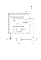
- FIG. 1 is a schematic sectional view showing a film forming apparatus according to an embodiment of the present invention.
- the film forming apparatus 10 of this embodiment is configured as a vacuum vapor deposition apparatus.
- the film forming apparatus 10 includes a vacuum chamber 11, a vapor deposition source 12 disposed inside the vacuum chamber 11, a stage 13 facing the vapor deposition source 12, and a film thickness sensor 14 disposed inside the vacuum chamber 11. Have.
- the vacuum chamber 11 is connected to an evacuation system 15 and is configured so that the inside can be maintained in a predetermined reduced pressure atmosphere.
- the vapor deposition source 12 is configured to be able to generate vapor (particles) of vapor deposition material.
- the vapor deposition source 12 is electrically connected to the power supply unit 18, and is an evaporation source that heats and evaporates the organic material (Alq3 (tris (8-quinolinolato) aluminum)) to release organic material particles. Constitute.
- the type of the evaporation source is not particularly limited, and various methods such as a resistance heating method, an induction heating method, and an electron beam heating method can be applied.
- the evaporation material may be an organic material other than those described above, or may be a metal material, a metal compound material, or the like.
- the stage 13 is configured to be able to hold a substrate W, which is a film formation target such as a semiconductor wafer or a glass substrate, toward the vapor deposition source 12.
- a substrate W which is a film formation target such as a semiconductor wafer or a glass substrate
- the film thickness sensor 14 (sensor head) incorporates a crystal resonator having a predetermined fundamental frequency (natural frequency), and measures the film thickness and film formation rate of the organic film deposited on the substrate W, as will be described later.
- the sensor head for this is comprised.
- the crystal resonator for example, an AT-cut crystal resonator having relatively excellent temperature characteristics is used, and the predetermined fundamental frequency is typically 5 to 6 MHz, and in this embodiment, 5 MHz. .
- the film thickness sensor 14 is disposed inside the vacuum chamber 11 and at a position facing the vapor deposition source 12. The film thickness sensor 14 is typically disposed in the vicinity of the stage 13.
- the output of the film thickness sensor 14 is supplied to the measurement unit 17 (film thickness control device).
- the measurement unit 17 measures the film thickness and the film formation rate based on the change in the oscillation frequency of the crystal resonator, and controls the vapor deposition source 12 so that the film formation rate becomes a predetermined value.
- the film thickness sensor 14 and the measurement unit 17 constitute a “film thickness monitor” according to the present invention.
- Equation (1) ⁇ Fs is the amount of frequency change, ⁇ m is the amount of mass change, f 0 is the fundamental frequency, ⁇ Q is the density of the crystal, ⁇ Q is the shear stress of the crystal, A is the electrode area, and N is a constant. ing.
- the film forming apparatus 10 further includes a shutter 16.
- the shutter 16 is disposed between the vapor deposition source 12 and the stage 13, and is configured to be able to open or shield the incident path of vapor deposition particles from the vapor deposition source 12 to the stage 13 and the film thickness sensor 14.
- the opening and closing of the shutter 16 is controlled by a control unit (not shown).
- the shutter 16 is closed at the start of vapor deposition until the release of vapor deposition particles at the vapor deposition source 12 is stable. And when discharge
- the vapor deposition particles from the vapor deposition source 12 reach the substrate W on the stage 13, and the film forming process of the substrate W is started.
- the vapor deposition particles from the vapor deposition source 12 reach the film thickness sensor 14, and the measurement unit 17 monitors the film thickness of the vapor deposition film on the substrate W and its film formation rate.
- FIG. 2 is a schematic block diagram illustrating a configuration example of the measurement unit 17.
- the measurement unit 17 includes an oscillation circuit 41, a measurement circuit 42, and a controller 43.
- the oscillation circuit 41 oscillates the crystal resonator 20 of the film thickness sensor 14.
- the measurement circuit 42 is for measuring the oscillation frequency of the crystal resonator 20 output from the oscillation circuit 41.
- the controller 43 obtains the oscillation frequency of the crystal unit 20 through the measurement circuit 42 every unit time, and calculates the deposition rate of the deposition material particles on the substrate W and the thickness of the deposition film deposited on the substrate W. To do.
- the controller 43 further controls the vapor deposition source 12 so that the film formation rate becomes a predetermined value.
- the measurement circuit 42 includes a mixer circuit 51, a low-pass filter 52, a low-frequency counter 53, a high-frequency counter 54, and a reference signal generation circuit 55.
- the signal output from the oscillation circuit 41 is input to the high frequency counter 54, and first, the approximate value of the oscillation frequency of the oscillation circuit 41 is measured.
- the approximate value of the oscillation frequency of the oscillation circuit 41 measured by the high frequency counter 54 is output to the controller 43.
- the controller 43 oscillates the reference signal generation circuit 55 at a reference frequency (for example, 5 MHz) that is close to the measured approximate value.
- a signal having a frequency oscillated at the reference frequency and a signal output from the oscillation circuit 41 are input to the mixer circuit 51.
- the mixer circuit 51 mixes the two types of input signals and outputs them to the low frequency counter 53 via the low pass filter 52.
- the signal input from the oscillation circuit 41 is cos (( ⁇ + ⁇ ) t) and the signal input from the reference signal generation circuit is cos ( ⁇ t)
- cos ( ⁇ t) ⁇ cos
- An AC signal expressed by the equation ( ⁇ + ⁇ ) t) is generated. This equation is in the form of multiplying cos ( ⁇ t) and cos (( ⁇ + ⁇ ) t), and the AC signal represented by this equation is a high frequency component represented by cos ((2 ⁇ ⁇ + ⁇ ) t). And a low frequency component signal represented by cos ( ⁇ t).
- the signal generated by the mixer circuit 51 is input to the low-pass filter 52, the high-frequency component signal cos ((2 ⁇ ⁇ + ⁇ ) t) is removed, and only the low-frequency component signal cos ( ⁇ t) is input to the low-frequency counter 53. Entered. That is, the low frequency counter 53 has a low frequency component that is an absolute value
- the low frequency counter 53 measures the frequency of the low frequency component signal and outputs the measured value to the controller 43.
- the controller 43 calculates the frequency of the signal output from the oscillation circuit 41 from the frequency measured by the low frequency counter 53 and the frequency of the output signal of the reference signal generation circuit 55. Specifically, when the frequency of the output signal of the reference signal generation circuit 55 is smaller than the frequency of the output signal of the oscillation circuit 41, the frequency of the low frequency component signal is added to the output signal of the oscillation circuit 41, In the opposite case, subtract.
- the oscillation frequency of the reference signal generation circuit 55 is It becomes lower than the actual oscillation frequency of the circuit 41. Therefore, in order to obtain the actual oscillation frequency of the oscillation circuit 41, the frequency
- the resolution of the low-frequency counter 53 has an upper limit, the resolution can be assigned to measure the difference frequency
- the oscillation frequency of the reference signal generation circuit 55 is controlled by the controller 43, and the oscillation frequency can be set so that the difference frequency
- the obtained frequency value is stored in the controller 43.
- the controller 43 calculates the film thickness and film formation rate of the vapor deposition material deposited on the substrate W from the obtained frequency value using the arithmetic expression shown by the above expression (1).
- the controller 43 can typically be realized by hardware elements used in a computer such as a CPU (Central Processing Unit), a RAM (Random Access Memory), and a ROM (Read Only Memory) and necessary software.
- a CPU Central Processing Unit
- RAM Random Access Memory
- ROM Read Only Memory
- PLD Programmable Logic Device
- FPGA Field Programmable Gate Array
- DSP Digital Signal Processor
- a method for determining the lifetime (replacement time) of the crystal resonator a method of measuring the equivalent resistance of the crystal resonator is known.
- the equivalent resistance exceeds a predetermined value, the crystal resonator is considered to have reached the end of life.
- the predetermined value in a crystal resonator having a fundamental frequency of 5 MHz is set to 20 ⁇ .
- a method of measuring the current flowing through the crystal resonator is also known, but this method is synonymous with measuring the equivalent resistance of the crystal resonator because the voltage applied to the crystal resonator is constant.
- FIG. 3 shows an example of measurement data when the film formation rate fluctuates greatly after the start of film formation and monitoring is no longer possible.
- the equivalent resistance of the quartz resonator at this time was measured and found to be 15.2 ⁇ , which was within the range considered normal (20 ⁇ or less).
- the film thickness sensor diagnosis method when determining the lifetime (replacement time) of the crystal resonator, the variation width of the change rate of the oscillation frequency is used as a reference, not the equivalent resistance of the crystal resonator.
- the film thickness sensor diagnosis method oscillates the crystal resonator 20 and measures the variation width of the change rate of the oscillation frequency of the crystal resonator 20, and when the variation width exceeds a predetermined value, The crystal unit 20 is determined to have a lifetime (cannot be used).
- the film thickness and the film formation rate are proportional to the rate of change of the oscillation frequency of the crystal unit 20. Therefore, the stable transition of the deposition rate means that the rate of change of the oscillation frequency of the crystal resonator 20 is stable.
- the crystal oscillation is determined by determining whether or not the lifetime of the crystal resonator 20 is based on the fluctuation range of the change rate of the oscillation frequency of the crystal resonator 20 (that is, the difference for each sampling of the oscillation frequency). An appropriate life determination of the child 20 can be performed. As a result, the life of the crystal unit 20 can be detected quickly, and deterioration of the film thickness control due to the life of the crystal unit 20 can be prevented.
- the lifetime determination of the crystal unit 20 described above is performed by the controller 43 in the measurement unit 17.
- the controller 43 calculates the fluctuation range ( ⁇ 2F) of the change rate ( ⁇ F) of the oscillation frequency (F) of the crystal resonator 20 measured in the measurement circuit 42, and whether or not the fluctuation range ( ⁇ 2F) exceeds a predetermined value.
- the crystal unit 20 is configured to be determined to have a lifetime.
- the predetermined value corresponds to a reference value for determining the life of the crystal unit 20, and can be set as appropriate according to the purpose.
- the predetermined value is set to 0.1 Hz, for example.
- the predetermined value may be, for example, a size that is considered to have reached the end of the life, or may be a predetermined size before it is considered that the end of the life has been reached.
- a plurality of the predetermined values may be set stepwise according to the magnitude of the fluctuation range.
- the standard deviation of the change rate of the oscillation frequency in a certain period may be measured. Thereby, while being able to reduce calculation load, a determination result can be acquired rapidly.
- the sample point is not particularly limited and can be set arbitrarily. In this case, when the standard deviation exceeds a predetermined value, it is determined that the lifetime of the crystal unit 20 is reached.
- the predetermined value of the standard deviation is, for example, 0.1 Hz.
- the controller 43 is configured to, for example, issue an alarm (for example, display on a screen, sound of a buzzer, light emission of a lamp) that prompts the user to replace the crystal unit 20. Is done.
- the controller 43 may be configured to automatically perform control to switch to a new crystal resonator, as will be described later.
- the measurement of the fluctuation range of the oscillation frequency of the crystal resonator 20 may be performed during film formation or may be performed during non-film formation.
- FIG. 4 is an experimental result showing an example of a change rate ( ⁇ F) of the oscillation frequency of the crystal resonator 20 during film formation and during non-film formation (during replacement of the substrate W).
- Alq3 tris (8-quinolinolato) aluminum was used as the vapor deposition material.
- the frequency change rate ( ⁇ F) in the normal crystal unit 20 is stable at an almost constant value regardless of whether the film is formed or not. Therefore, it is possible to determine the life of the crystal unit 20 based on the fluctuation width ( ⁇ 2F) of the frequency change rate during film formation or during non-film formation.
- FIG. 5 is a partially enlarged view of measurement data at the time of non-deposition in FIG. 4
- FIG. 6 is a partially enlarged view of measurement data at the time of film formation in FIG.
- the fluctuation width ( ⁇ 2F) of the change rate of the oscillation frequency is kept within 0.03 Hz during non-film formation and during film formation.
- the standard deviation of the fluctuation range ( ⁇ 2F) was 0.005 Hz for both the non-film formation and the film formation.
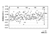
- FIG. 7 shows one measurement data indicating the rate of change ( ⁇ F) of the oscillation frequency of the crystal unit 20 determined to have reached the end of its life.
- the fluctuation range ( ⁇ 2F) at this time was 2 Hz, and the standard deviation was 0.5 Hz.
- the crystal resonator 20 has a defect or life ( ⁇ F2) of the oscillation frequency change rate or its standard deviation before or during film formation.
- the replacement time can be determined appropriately and easily.
- the lifetime of the crystal unit 20 can be quickly determined when forming an organic film that reaches the end of its life relatively early.
- the life of the crystal unit 20 can also be determined from the fluctuation range of the film formation rate.
- the film formation rate is converted to the film thickness from the frequency change and the density of the vapor deposition material, and more often multiplied by a correction coefficient related to the sensor position with respect to the substrate, from the viewpoint of determining the lifetime of the crystal unit, It is more essential to look at the fluctuation of the frequency change rate of the crystal unit itself.
- FIG. 8 is a schematic configuration diagram showing the film thickness monitor 100 according to the present embodiment.
- the film thickness monitor 100 includes a film thickness sensor 140 (sensor head) and a measurement unit 17.
- the film thickness sensor 140 includes a holder 141 that can support a plurality of crystal resonators (12 in this example) 201 to 212, and a casing 142 that rotatably accommodates the holder 141.
- the holder 141 has a disk shape, and the plurality of crystal resonators 201 to 212 are mounted near the periphery of the holder 141 at equal angular intervals.
- the holder 141 is configured to be able to rotate intermittently at the same angular interval in the direction of the arrow in the figure inside the casing 142.
- the casing 142 includes a rotating shaft 142a that rotatably supports the holder 141, and a drive mechanism (not shown) that rotates the holder 141 around the rotating shaft 142a.
- the drive mechanism is configured to rotate the holder 141 by a predetermined angle in the direction of the arrow in the figure in accordance with a control signal input from the measurement unit 17.
- the casing 142 has a window portion 143 that exposes only one crystal resonator of the plurality of crystal resonators 201 to 212 attached to the holder 141 to the outside (deposition source 12). In the illustrated example, the crystal unit 201 is exposed through the window portion 143.
- the casing 142 is provided with an electrode unit 144 for electrically connecting the crystal resonator at the rotational position of the window 143 to the measurement unit 17.
- the electrode unit 144 is disposed in the vicinity of the window portion 143 and is configured to come into contact with the crystal resonator that has been moved to a position facing the window portion 143 by the rotation of the holder 141.
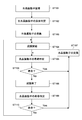
- FIG. 9 shows an operation procedure of the film forming apparatus including an operation example of the film thickness monitor 100.
- the crystal resonators 201 to 212 are mounted on the holder 141 of the film thickness sensor 140 (step 101).
- the crystal resonators 201 to 212 are the same type of crystal resonator.
- the quality of the oscillation operation is determined for all the crystal resonators 201 to 212 (step 102).
- the holder 141 is intermittently rotated to connect all the crystal oscillators 201 to 212 to the electrode unit 144 in sequence, and the measurement unit 17 causes each oscillator to oscillate at a predetermined drive voltage for a predetermined time.
- the measurement unit 17 measures the fluctuation range of the change rate of the oscillation frequency of the crystal resonator, and determines that the crystal resonator that exceeds a predetermined value is defective.
- the crystal resonator determined to be defective is replaced with another new crystal resonator (step 103).
- the quality determination of the crystal resonators 201 to 212 is a preliminary one for confirming the characteristics of the crystal resonators 201 to 212, and can be omitted as necessary. According to the present embodiment, as described in the first embodiment, the fact that the rate of change of the oscillation frequency of the crystal resonator during non-film formation is stable is utilized. Based on the standard deviation, the quality of the oscillation operation of each of the crystal resonators 201 to 212 is determined.
- the substrate W is placed on the stage 13, and the vapor deposition material is supplied to the vapor deposition source 12, and then the vacuum chamber 11 is evacuated to a predetermined reduced pressure atmosphere by the vacuum exhaust system 15. Then, the shutter 16 is opened, and deposition of a vapor deposition material on the substrate W is started (step 104).
- the film thickness monitor 100 monitors the film thickness and film formation rate of the vapor deposition material deposited on the surface of the substrate W using the crystal unit 201.
- the controller 43 of the measurement unit 17 measures the fluctuation range of the change rate of the oscillation frequency of the crystal resonator 201 during film formation, so that the crystal resonator can reach the end of its life in the same manner as in the first embodiment. It is determined whether or not it has been reached (step 105). When the controller 43 determines that the crystal resonator 201 has not reached the end of its life, the controller 43 continues oscillation.
- the controller 43 outputs a control signal to the film thickness sensor 140 in order to replace the crystal resonator 201 with a new crystal resonator 202 (step 106, 107).
- the holder 141 rotates by a predetermined angle in the direction of the arrow in FIG. 8, so that the crystal unit 202 is disposed at a position facing the window 143 instead of the crystal unit 201 and is connected to the electrode unit 144. The Thereafter, rate measurement and film thickness measurement using the crystal resonator 202 are performed.
- the replacement from the crystal unit 201 to the crystal unit 202 is typically performed without interrupting film formation on the substrate W.
- the measurement data of the crystal unit 201 immediately before the replacement and the measurement data of the crystal unit 202 immediately after the replacement are used in combination for the measurement of the film thickness and the film formation rate during the replacement.
- step 108 When film formation with a predetermined thickness on the substrate W is completed (step 108), the shutter 16 is closed as shown in FIG. At this time, the measurement unit 17 continues the oscillation operation of the crystal resonator 202 of the film thickness sensor 140, and determines the life of the crystal resonator 202 based on the fluctuation range of the frequency change rate at this time (step 109).
- the holder 141 is rotated as described above to switch the crystal unit 202 to the next crystal unit 203 (steps 110 and 107).
- film formation using the crystal resonator 202 is subsequently started (step 110, 104).
- the film forming process is performed on the plurality of substrates W by repeating the above-described operation.
- the film thickness sensor 140 is continuously used until all the crystal resonators 201 to 212 reach the end of their lives. Thereby, the throughput of the film forming apparatus 10 is improved, and productivity can be improved.
- the crystal resonators 201 to 212 are defective.
- the lifetime (replacement time) can be determined.
- the life of the crystal resonator is determined both during film formation and during non-film formation, but the life determination of the crystal resonator is performed during film formation and during non-deposition. It may be performed only at any one of the time of filming.
- the crystal resonator determined to be defective was replaced with a non-defective product, but instead of this, the crystal determined to be defective was replaced.
- the vibrator may be mounted as it is, and only the crystal vibrator that is determined to be a non-defective product by the controller 43 may be selected and switched.
- the vacuum deposition apparatus has been described as an example of the film forming apparatus.
- the present invention is not limited to this, and the present invention can be applied to other film forming apparatuses such as a sputtering apparatus.
- the vapor deposition source is composed of a sputtering cathode including a target.
Landscapes
- Chemical & Material Sciences (AREA)
- Chemical Kinetics & Catalysis (AREA)
- Engineering & Computer Science (AREA)
- Materials Engineering (AREA)
- Mechanical Engineering (AREA)
- Metallurgy (AREA)
- Organic Chemistry (AREA)
- Physics & Mathematics (AREA)
- General Physics & Mathematics (AREA)
- Health & Medical Sciences (AREA)
- Life Sciences & Earth Sciences (AREA)
- Analytical Chemistry (AREA)
- Biochemistry (AREA)
- General Health & Medical Sciences (AREA)
- Immunology (AREA)
- Pathology (AREA)
- Length Measuring Devices Characterised By Use Of Acoustic Means (AREA)
Abstract
Description
例えば、金属膜の場合では、着膜量の増加に伴って、水晶振動子の発振周波数が徐々に低下し、所定の周波数に達すると突然、発振周波数が大きく変化する。したがって発振周波数の急変を確認するまでは比較的安定に膜厚を測定することができるため、発振周波数の急変が生じた段階で当該水晶振動子を使用できない状態(すなわち寿命)であると判断することができる。
これに対して有機膜の場合には、着膜量の増加に伴って、水晶振動子の発振周波数が低下すると同時に、もはや安定した膜厚測定を行うことができないほどに周波数の変動が大きくなる。したがって有機膜を成膜する場合は、金属膜を成膜する場合と比較して、測定可能な膜厚量が非常に少ない。このため、安定した成膜処理を実施する上では、水晶振動子の適正な寿命判定が不可欠となる。
上記水晶振動子の発振周波数の変化率の変動幅が測定される。
上記変動幅が所定値を超えるときは、上記水晶振動子は使用できないと判定される。
上記センサヘッドは、第1および第2の水晶振動子を支持するホルダと、上記ホルダを回転可能に収容するケーシングとを有する。
上記測定ユニットは、上記第1および第2の水晶振動子の発振周波数の変化率の変動幅を各々測定し、前記変動幅が所定値を超える水晶振動子を使用できないと判定するように構成される。
これにより、膜厚測定用の振動子を、第1の水晶振動子から第2の水晶振動子へ自動的に切り替えることができる。
図1は、本発明の一実施形態に係る成膜装置を示す概略断面図である。本実施形態の成膜装置10は、真空蒸着装置として構成される。

図2は、測定ユニット17の一構成例を示す概略ブロック図である。測定ユニット17は、発振回路41と、測定回路42と、コントローラ43とを有する。
ところで、この種の膜厚センサは、有機膜を成膜する場合、着膜量の増加に伴って、水晶振動子の発振周波数が徐々に低下すると同時に、もはや安定した膜厚測定を行うことができないほどに周波数の変動が大きくなる。したがって有機膜を成膜する場合は、金属膜を成膜する場合と比較して、測定可能な膜厚量が非常に少ない。このため、安定した成膜処理を実施する上では、水晶振動子の適正な寿命判定が不可欠となる。
続いて、本発明の他の実施形態について説明する。以下、第1の実施形態と異なる構成について主に説明し、上述の実施形態と同様の構成については同様の符号を付しその説明を省略または簡略化する。
11…真空チャンバ
12…蒸着源
13…ステージ
14,140…膜厚センサ
17…測定ユニット
18…電源ユニット
20,201~212…水晶振動子
43…コントローラ
100…膜厚モニタ
141…ホルダ
142…ケーシング
143…窓部
144…電極ユニット
Claims (8)
- 水晶振動子を有する膜厚センサの診断方法であって、
センサヘッドに装着された水晶振動子を発振させ、
前記水晶振動子の発振周波数の変化率の変動幅を測定し、
前記変動幅が所定値を超えるときは、前記水晶振動子を使用できないと判定する
膜厚センサの診断方法。 - 請求項1に記載の膜厚センサの診断方法であって、
前記変動幅を、成膜時に測定する
膜厚センサの診断方法。 - 請求項1に記載の膜厚センサの診断方法であって、
前記変動幅を、非成膜時に測定する
膜厚センサの診断方法。 - 請求項1から3のいずれか1つに記載の膜厚センサの診断方法であって、
前記変動幅を測定する工程では、一定期間における前記発振周波数の変化率の変動幅の標準偏差が測定される
膜厚センサの診断方法。 - 請求項1~4のいずれか1つに記載の膜厚センサの診断方法であって、
前記水晶振動子の使用可否の判定を、有機膜の成膜のときに実行する
膜厚センサの診断方法。 - 第1および第2の水晶振動子を支持するホルダと、前記ホルダを回転可能に収容するケーシングとを有するセンサヘッドと、
前記第1および第2の水晶振動子の発振周波数の変化率の変動幅を各々測定し、前記変動幅が所定値を超える水晶振動子を使用できないと判定する測定ユニットと
を具備する膜厚モニタ。 - 請求項6に記載の膜厚モニタであって、
前記ケーシングは、前記第1の水晶振動子に対向して形成され蒸着物質が通過可能な窓部をさらに有し、
前記測定ユニットは、前記第1の水晶振動子を使用できないと判定したときは、前記第2の水晶振動子が前記窓部に対向する位置に前記ホルダを回転させる
膜厚モニタ。 - 請求項6または7に記載の膜厚モニタであって、
前記測定ユニットは、前記変動幅を成膜時または非成膜時に測定する
膜厚モニタ。
Priority Applications (3)
| Application Number | Priority Date | Filing Date | Title |
|---|---|---|---|
| JP2016537739A JP6333386B2 (ja) | 2014-07-31 | 2015-07-21 | 水晶振動子の交換方法および膜厚モニタ |
| KR1020177000979A KR101890540B1 (ko) | 2014-07-31 | 2015-07-21 | 수정 진동자의 교환 방법 및 막후 모니터 |
| CN201580041086.5A CN106574833B (zh) | 2014-07-31 | 2015-07-21 | 膜厚传感器的诊断方法以及膜厚监视器 |
Applications Claiming Priority (2)
| Application Number | Priority Date | Filing Date | Title |
|---|---|---|---|
| JP2014156220 | 2014-07-31 | ||
| JP2014-156220 | 2014-07-31 |
Publications (1)
| Publication Number | Publication Date |
|---|---|
| WO2016017108A1 true WO2016017108A1 (ja) | 2016-02-04 |
Family
ID=55217029
Family Applications (1)
| Application Number | Title | Priority Date | Filing Date |
|---|---|---|---|
| PCT/JP2015/003643 Ceased WO2016017108A1 (ja) | 2014-07-31 | 2015-07-21 | 膜厚センサの診断方法および膜厚モニタ |
Country Status (4)
| Country | Link |
|---|---|
| JP (1) | JP6333386B2 (ja) |
| KR (1) | KR101890540B1 (ja) |
| CN (1) | CN106574833B (ja) |
| WO (1) | WO2016017108A1 (ja) |
Cited By (3)
| Publication number | Priority date | Publication date | Assignee | Title |
|---|---|---|---|---|
| TWI683089B (zh) * | 2016-09-06 | 2020-01-21 | 日商愛發科股份有限公司 | 膜厚感測器 |
| JP2020033620A (ja) * | 2018-08-31 | 2020-03-05 | キヤノントッキ株式会社 | 成膜装置及び成膜装置の制御方法 |
| JP2022090053A (ja) * | 2018-08-31 | 2022-06-16 | キヤノントッキ株式会社 | 成膜装置及び成膜装置の制御方法 |
Families Citing this family (6)
| Publication number | Priority date | Publication date | Assignee | Title |
|---|---|---|---|---|
| US10767987B2 (en) * | 2017-06-28 | 2020-09-08 | Ulvac, Inc. | Sensor head for crystal oscillator type of film thickness monitor |
| CN107565062B (zh) * | 2017-07-20 | 2019-10-11 | 武汉华星光电半导体显示技术有限公司 | 膜厚监控仪与蒸镀机 |
| KR101870581B1 (ko) * | 2017-09-29 | 2018-06-22 | 캐논 톡키 가부시키가이샤 | 수정진동자의 수명 판정방법, 막두께 측정장치, 성막방법, 성막장치, 및 전자 디바이스 제조방법 |
| JP7144232B2 (ja) * | 2018-08-08 | 2022-09-29 | キヤノントッキ株式会社 | 成膜レートモニタ装置及び成膜装置 |
| CN110257775A (zh) * | 2019-06-17 | 2019-09-20 | 深圳市华星光电技术有限公司 | 蒸镀装置及蒸镀方法 |
| CN121409162A (zh) * | 2025-12-30 | 2026-01-27 | 浙江同越光学科技有限公司 | 一种多晶片石英晶体膜厚监测装置及其使用方法 |
Citations (6)
| Publication number | Priority date | Publication date | Assignee | Title |
|---|---|---|---|---|
| JPH05162562A (ja) * | 1991-12-12 | 1993-06-29 | Toyota Motor Corp | 居眠り運転検出装置 |
| JPH07183049A (ja) * | 1993-12-24 | 1995-07-21 | Shin Kobe Electric Mach Co Ltd | 蓄電池の劣化状態推定方法及び装置 |
| JPH11160057A (ja) * | 1997-11-28 | 1999-06-18 | Ulvac Corp | 圧電結晶発振式膜厚計 |
| JP2005515438A (ja) * | 2002-01-09 | 2005-05-26 | フィッシャー コントロールズ インターナショナル リミテッド ライアビリティー カンパニー | 化学検出システムを診断する装置および方法 |
| JP2008276998A (ja) * | 2007-04-26 | 2008-11-13 | Sony Corp | 膜厚センサ、薄膜形成装置、有機el表示装置の製造装置、及び有機el表示装置の製造方法 |
| JP2014070969A (ja) * | 2012-09-28 | 2014-04-21 | Hitachi High-Technologies Corp | レートセンサ及びリニアソース並びに蒸着装置 |
Family Cites Families (3)
| Publication number | Priority date | Publication date | Assignee | Title |
|---|---|---|---|---|
| JP3953301B2 (ja) * | 2001-11-05 | 2007-08-08 | 株式会社アルバック | 水晶発振式膜厚モニタ用センサヘッド |
| KR101283161B1 (ko) * | 2007-09-21 | 2013-07-05 | 가부시키가이샤 알박 | 박막 형성 장치, 막두께 측정 방법, 막두께 센서 |
| JP5888919B2 (ja) * | 2010-11-04 | 2016-03-22 | キヤノン株式会社 | 成膜装置及び成膜方法 |
-
2015
- 2015-07-21 CN CN201580041086.5A patent/CN106574833B/zh active Active
- 2015-07-21 KR KR1020177000979A patent/KR101890540B1/ko active Active
- 2015-07-21 JP JP2016537739A patent/JP6333386B2/ja active Active
- 2015-07-21 WO PCT/JP2015/003643 patent/WO2016017108A1/ja not_active Ceased
Patent Citations (6)
| Publication number | Priority date | Publication date | Assignee | Title |
|---|---|---|---|---|
| JPH05162562A (ja) * | 1991-12-12 | 1993-06-29 | Toyota Motor Corp | 居眠り運転検出装置 |
| JPH07183049A (ja) * | 1993-12-24 | 1995-07-21 | Shin Kobe Electric Mach Co Ltd | 蓄電池の劣化状態推定方法及び装置 |
| JPH11160057A (ja) * | 1997-11-28 | 1999-06-18 | Ulvac Corp | 圧電結晶発振式膜厚計 |
| JP2005515438A (ja) * | 2002-01-09 | 2005-05-26 | フィッシャー コントロールズ インターナショナル リミテッド ライアビリティー カンパニー | 化学検出システムを診断する装置および方法 |
| JP2008276998A (ja) * | 2007-04-26 | 2008-11-13 | Sony Corp | 膜厚センサ、薄膜形成装置、有機el表示装置の製造装置、及び有機el表示装置の製造方法 |
| JP2014070969A (ja) * | 2012-09-28 | 2014-04-21 | Hitachi High-Technologies Corp | レートセンサ及びリニアソース並びに蒸着装置 |
Cited By (5)
| Publication number | Priority date | Publication date | Assignee | Title |
|---|---|---|---|---|
| TWI683089B (zh) * | 2016-09-06 | 2020-01-21 | 日商愛發科股份有限公司 | 膜厚感測器 |
| JP2020033620A (ja) * | 2018-08-31 | 2020-03-05 | キヤノントッキ株式会社 | 成膜装置及び成膜装置の制御方法 |
| JP7064407B2 (ja) | 2018-08-31 | 2022-05-10 | キヤノントッキ株式会社 | 成膜装置及び成膜装置の制御方法 |
| JP2022090053A (ja) * | 2018-08-31 | 2022-06-16 | キヤノントッキ株式会社 | 成膜装置及び成膜装置の制御方法 |
| JP7262647B2 (ja) | 2018-08-31 | 2023-04-21 | キヤノントッキ株式会社 | 成膜装置及び成膜装置の制御方法 |
Also Published As
| Publication number | Publication date |
|---|---|
| KR20170018418A (ko) | 2017-02-17 |
| JPWO2016017108A1 (ja) | 2017-04-27 |
| CN106574833A (zh) | 2017-04-19 |
| JP6333386B2 (ja) | 2018-05-30 |
| CN106574833B (zh) | 2019-12-31 |
| KR101890540B1 (ko) | 2018-08-21 |
Similar Documents
| Publication | Publication Date | Title |
|---|---|---|
| JP6333386B2 (ja) | 水晶振動子の交換方法および膜厚モニタ | |
| CN111829428B (zh) | 一种双石英晶振膜厚控制仪及误差校正方法 | |
| JP6078694B2 (ja) | 成膜装置、有機膜の膜厚測定方法および有機膜用膜厚センサ | |
| JP6328253B2 (ja) | 膜厚モニタおよび膜厚測定方法 | |
| JP6564745B2 (ja) | 膜厚センサ | |
| KR20150135082A (ko) | 수정 발진식 막두께 모니터에 의한 막두께 제어 방법 | |
| JPWO2016140321A1 (ja) | 膜厚監視装置用センサ、それを備えた膜厚監視装置、および膜厚監視装置用センサの製造方法 | |
| JP6060319B2 (ja) | 膜厚制御装置、膜厚制御方法および成膜装置 | |
| JP7217822B1 (ja) | 膜厚監視方法および膜厚監視装置 | |
| JP6412384B2 (ja) | 水晶振動子、この水晶振動子を有するセンサヘッド、成膜制御装置、および成膜制御装置の製造方法 | |
| JP2019099870A (ja) | 蒸着装置及び蒸着方法 | |
| JP7509926B2 (ja) | イオンミリング装置 | |
| JPH1123245A (ja) | 水晶振動子法蒸着膜厚測定装置 | |
| JP5839868B2 (ja) | 膜厚測定方法および膜厚測定システム | |
| JP2023006990A (ja) | センサ装置 | |
| JP2016042643A (ja) | 膜厚モニタ用発振回路 | |
| JP2007059659A (ja) | 半導体製造装置 | |
| JP2022022859A (ja) | 測定装置、膜厚センサ、成膜装置および異常判定方法 |
Legal Events
| Date | Code | Title | Description |
|---|---|---|---|
| 121 | Ep: the epo has been informed by wipo that ep was designated in this application |
Ref document number: 15827294 Country of ref document: EP Kind code of ref document: A1 |
|
| ENP | Entry into the national phase |
Ref document number: 2016537739 Country of ref document: JP Kind code of ref document: A |
|
| ENP | Entry into the national phase |
Ref document number: 20177000979 Country of ref document: KR Kind code of ref document: A |
|
| NENP | Non-entry into the national phase |
Ref country code: DE |
|
| 122 | Ep: pct application non-entry in european phase |
Ref document number: 15827294 Country of ref document: EP Kind code of ref document: A1 |