WO2016010061A1 - 自己組織化膜形成材料として有用なトリプチセン誘導体、その製造方法、それを用いた膜、当該膜の製造方法、及びそれを用いた電子デバイス - Google Patents
自己組織化膜形成材料として有用なトリプチセン誘導体、その製造方法、それを用いた膜、当該膜の製造方法、及びそれを用いた電子デバイス Download PDFInfo
- Publication number
- WO2016010061A1 WO2016010061A1 PCT/JP2015/070220 JP2015070220W WO2016010061A1 WO 2016010061 A1 WO2016010061 A1 WO 2016010061A1 JP 2015070220 W JP2015070220 W JP 2015070220W WO 2016010061 A1 WO2016010061 A1 WO 2016010061A1
- Authority
- WO
- WIPO (PCT)
- Prior art keywords
- group
- film
- carbon atoms
- atom
- compound
- Prior art date
- Legal status (The legal status is an assumption and is not a legal conclusion. Google has not performed a legal analysis and makes no representation as to the accuracy of the status listed.)
- Ceased
Links
Images




Classifications
-
- H—ELECTRICITY
- H10—SEMICONDUCTOR DEVICES; ELECTRIC SOLID-STATE DEVICES NOT OTHERWISE PROVIDED FOR
- H10K—ORGANIC ELECTRIC SOLID-STATE DEVICES
- H10K10/00—Organic devices specially adapted for rectifying, amplifying, oscillating or switching; Organic capacitors or resistors having potential barriers
- H10K10/40—Organic transistors
- H10K10/46—Field-effect transistors, e.g. organic thin-film transistors [OTFT]
- H10K10/462—Insulated gate field-effect transistors [IGFETs]
- H10K10/468—Insulated gate field-effect transistors [IGFETs] characterised by the gate dielectrics
- H10K10/471—Insulated gate field-effect transistors [IGFETs] characterised by the gate dielectrics the gate dielectric comprising only organic materials
-
- C—CHEMISTRY; METALLURGY
- C07—ORGANIC CHEMISTRY
- C07C—ACYCLIC OR CARBOCYCLIC COMPOUNDS
- C07C43/00—Ethers; Compounds having groups, groups or groups
- C07C43/02—Ethers
- C07C43/20—Ethers having an ether-oxygen atom bound to a carbon atom of a six-membered aromatic ring
- C07C43/21—Ethers having an ether-oxygen atom bound to a carbon atom of a six-membered aromatic ring containing rings other than six-membered aromatic rings
-
- C—CHEMISTRY; METALLURGY
- C07—ORGANIC CHEMISTRY
- C07C—ACYCLIC OR CARBOCYCLIC COMPOUNDS
- C07C43/00—Ethers; Compounds having groups, groups or groups
- C07C43/02—Ethers
- C07C43/20—Ethers having an ether-oxygen atom bound to a carbon atom of a six-membered aromatic ring
- C07C43/215—Ethers having an ether-oxygen atom bound to a carbon atom of a six-membered aromatic ring having unsaturation outside the six-membered aromatic rings
-
- C—CHEMISTRY; METALLURGY
- C07—ORGANIC CHEMISTRY
- C07C—ACYCLIC OR CARBOCYCLIC COMPOUNDS
- C07C43/00—Ethers; Compounds having groups, groups or groups
- C07C43/02—Ethers
- C07C43/20—Ethers having an ether-oxygen atom bound to a carbon atom of a six-membered aromatic ring
- C07C43/225—Ethers having an ether-oxygen atom bound to a carbon atom of a six-membered aromatic ring containing halogen
-
- H—ELECTRICITY
- H01—ELECTRIC ELEMENTS
- H01B—CABLES; CONDUCTORS; INSULATORS; SELECTION OF MATERIALS FOR THEIR CONDUCTIVE, INSULATING OR DIELECTRIC PROPERTIES
- H01B1/00—Conductors or conductive bodies characterised by the conductive materials; Selection of materials as conductors
- H01B1/06—Conductors or conductive bodies characterised by the conductive materials; Selection of materials as conductors mainly consisting of other non-metallic substances
- H01B1/12—Conductors or conductive bodies characterised by the conductive materials; Selection of materials as conductors mainly consisting of other non-metallic substances organic substances
- H01B1/121—Charge-transfer complexes
-
- H—ELECTRICITY
- H10—SEMICONDUCTOR DEVICES; ELECTRIC SOLID-STATE DEVICES NOT OTHERWISE PROVIDED FOR
- H10D—INORGANIC ELECTRIC SEMICONDUCTOR DEVICES
- H10D30/00—Field-effect transistors [FET]
- H10D30/60—Insulated-gate field-effect transistors [IGFET]
- H10D30/67—Thin-film transistors [TFT]
-
- H—ELECTRICITY
- H10—SEMICONDUCTOR DEVICES; ELECTRIC SOLID-STATE DEVICES NOT OTHERWISE PROVIDED FOR
- H10K—ORGANIC ELECTRIC SOLID-STATE DEVICES
- H10K10/00—Organic devices specially adapted for rectifying, amplifying, oscillating or switching; Organic capacitors or resistors having potential barriers
- H10K10/40—Organic transistors
- H10K10/46—Field-effect transistors, e.g. organic thin-film transistors [OTFT]
- H10K10/462—Insulated gate field-effect transistors [IGFETs]
- H10K10/466—Lateral bottom-gate IGFETs comprising only a single gate
-
- H—ELECTRICITY
- H10—SEMICONDUCTOR DEVICES; ELECTRIC SOLID-STATE DEVICES NOT OTHERWISE PROVIDED FOR
- H10K—ORGANIC ELECTRIC SOLID-STATE DEVICES
- H10K10/00—Organic devices specially adapted for rectifying, amplifying, oscillating or switching; Organic capacitors or resistors having potential barriers
- H10K10/40—Organic transistors
- H10K10/46—Field-effect transistors, e.g. organic thin-film transistors [OTFT]
- H10K10/462—Insulated gate field-effect transistors [IGFETs]
- H10K10/468—Insulated gate field-effect transistors [IGFETs] characterised by the gate dielectrics
- H10K10/474—Insulated gate field-effect transistors [IGFETs] characterised by the gate dielectrics the gate dielectric comprising a multilayered structure
-
- C—CHEMISTRY; METALLURGY
- C07—ORGANIC CHEMISTRY
- C07C—ACYCLIC OR CARBOCYCLIC COMPOUNDS
- C07C2603/00—Systems containing at least three condensed rings
- C07C2603/56—Ring systems containing bridged rings
- C07C2603/90—Ring systems containing bridged rings containing more than four rings
Definitions
- the present invention relates to a triptycene derivative useful as a material for forming a self-assembled monolayer (SAM), a manufacturing method thereof, a film using the same, and a manufacturing method thereof.
- SAM self-assembled monolayer
- the self-assembled monomolecular film is adsorbed or chemically bonded to the surface of a solid substrate, and is formed as a monomolecular layer (film) with high orientation by interaction between molecules.
- the self-assembled monomolecular film is referred to as a self-assembled monomolecular film or a self-assembled monomolecular film, but is referred to as a self-assembled monomolecular film or simply a SAM film in this specification. It was reported that the SAM film was formed on a glass substrate using an organosilane compound (see Non-Patent Document 1), and that it was formed on a gold substrate using an organic sulfur compound ( From Non-Patent Document 2), it has developed rapidly.
- the SAM film is more stable than an LB (Langmuir-Blodgett) film, and can be formed by a gas phase reaction, and its application range has been widened.
- the film thickness of the SAM film is determined by the molecular size (length) and the tilt angle with the substrate, and a film of a molecular level of about 1 nm can be precisely and easily manufactured.
- the film thickness is generally about 0.2 nm due to one methylene unit of the alkyl chain, and a monomolecular film with a desired film thickness can be accurately produced by adjusting the length of the alkyl chain. .
- the characteristics of the surface of the solid substrate can be modified.
- organic field effect transistor silicon oxide is often used as an insulating layer, but a SAM film made of an organic silane compound such as octadecyltrichlorosilane (OTS) is formed on the surface of the silicon oxide.
- OTS octadecyltrichlorosilane
- a specific function can be imparted to the surface of the solid substrate by bonding a functional functional group to one of the molecules forming the SAM film.
- various functions such as electron transfer / redox reaction, catalysis, photoinduced electron transfer, electrochemical luminescence, ion / molecule recognition, biosensor, biomolecular device, solar power generation, etc. can be achieved by forming a SAM film. It can be applied to the surface of a solid substrate and is expected to be applied in these fields.
- Non-Patent Document 3 it has been reported that triptycene derivatives substituted with 1, 2, 5, or 6 long-chain alkoxy groups are regularly aligned to form a smectic liquid crystal. It is not disclosed until the three substituents are regularly aligned in the same direction, nor is it disclosed that it is suitable as a SAM film forming material.
- triptycene derivatives in which three identical substituents are regularly aligned in the same direction accumulate these aligned substituents in the same direction to form a film. It has been reported that the film thus formed is self-organized and can be processed into a self-assembled monolayer by further processing (see Patent Document 16).
- JP 2002-363154 A International Publication No. 2003-055853 JP 2004-33824 A JP 2004-315461 A JP 2007-277171 A JP2012-111716A Special Table 2002-539286 JP 2004-359599 A JP-T-2004-506791 JP 2006-1968 A JP-T-2006-512472 JP 2006-187225 A JP 2008-75047 A JP 2008-308433 A JP 2010-248467 A PCT / JP2013 / 004952
- the present invention provides a novel Janus-type triptycene derivative represented by the following general formula [I], which is useful as a material material of a self-assembled film, particularly a self-assembled monolayer, and a method for producing the same.
- the present invention also provides a film forming material containing a Janus type triptycene derivative represented by the following general formula [I], and a self-organization using the Janus type triptycene derivative represented by the following general formula [I].
- Provided are a chemical film, a solid substrate having the film on the surface, and a method for producing the film.
- the present invention provides a highly efficient, highly homogeneous, and highly stable electronic device by forming a very uniform interface between an insulator and an organic semiconductor.
- the electronic device of the present invention realizes an electronic device with a low noise level because the interface between the insulator and the organic semiconductor is extremely uniform, thereby detecting a weak signal, for example, a signal emitted by a living body with high sensitivity. enable.
- the film forming the interface of the present invention can be flexible and have a large area, and a large area and flexible electronic device can be provided.
- the present inventors have examined the introduction of a plurality of functional groups into triptycene in a position-specific and surface-specific manner. Then, the inventors of the present invention have found that triptycene derivatives having three identical substituents on one side of triptycene are surface-specifically accumulated in a triple benzene ring arranged in triptycene, and It has been found that when three identical substituents have relatively long carbon chains, these substituents are aligned and accumulated in the same direction to form a film (see Patent Document 16).
- R 1 represents a saturated or unsaturated divalent hydrocarbon group having 2 to 60 carbon atoms, and the hydrocarbon group may have one or two or more substituents; , One or more carbon atoms in the hydrocarbon group are an oxygen atom, a sulfur atom, a silicon atom, or —NR 5 — (wherein R 5 is a hydrogen atom, an alkyl having 1 to 10 carbon atoms) Or an aryl group having 6 to 30 carbon atoms).
- R 2 represents a hydrogen atom or a saturated or unsaturated hydrocarbon group having 1 to 4 carbon atoms
- R 3 represents a group —R 1 —Z, a hydrogen atom, or a saturated or unsaturated hydrocarbon group having 1 to 4 carbon atoms
- Three R 4 s may be the same or different and each independently has a hydrogen atom, a halogen atom, a hydroxyl group, a nitro group, a cyano group, an amino group, a monoalkyl-substituted amino group, a dialkyl-substituted amino group, or a substituent.
- the present invention also relates to a film forming material composition comprising a Janus triptycene derivative represented by the above general formula [I]. Furthermore, the present invention has a film in which the Janus-type triptycene derivative represented by the above general formula [I] is self-organized, particularly a self-assembled monomolecular film, and the film on the surface of a solid substrate. Regarding the structure.
- the Janus triptycene derivative represented by the general formula [I] is dissolved in a solvent to form a solution, and the solution is applied to the surface of the solid substrate or the solid substrate is immersed in the solution,
- the present invention relates to a method for producing a Janus triptycene derivative film represented by the above general formula [I] on the surface of a solid substrate, which is dried and further annealed as necessary.
- the Janus triptycene derivative represented by the general formula [I] is dissolved in a solvent to form a solution, and the solution is applied to the surface of the solid substrate or the solid substrate is immersed in the solution,
- the present invention relates to a method for producing a structure in which a film of a Janus triptycene derivative represented by the above general formula [I] is formed on the surface of a solid substrate, which is dried and further annealed as necessary.
- the present invention relates to an electronic device comprising as a constituent element a film comprising a Janus type triptycene derivative represented by the above general formula [I].
- X in the general formula [I] is —CH 2 —, —CH ⁇ CH—, —O—, or —NR 6 — (wherein R 6 is a hydrogen atom or having 1 to 4 carbon atoms)
- R 1 in the general formula [I] represents an alkylene group having 2 to 30 carbon atoms, an alkenylene group having 2 to 30 carbon atoms, an alkynylene group having 2 to 30 carbon atoms, or an aryl ring having 6 to 30 carbon atoms.
- R 1 in the general formula [I] is an alkylene group having 2 to 30 carbon atoms or a divalent arylene group having 6 to 60 carbon atoms containing an aryl ring having 6 to 30 carbon atoms, The Janus type triptycene derivative according to the above (6).
- Z in the general formula [I] is a hydrogen atom, a haloalkyl group having 1 to 10 carbon atoms, an alkenyl group having 2 to 10 carbon atoms, an alkynyl group having 2 to 10 carbon atoms, a hydroxyl group, —COOR 7 (where , R 7 represents a hydrogen atom or an optionally substituted alkyl group having 1 to 5 carbon atoms), —N (R 8 ) 2 (wherein R 8 may be the same or different, and Or a hydrogen atom, an optionally substituted alkyl group having 1 to 5 carbon atoms, or an optionally substituted aryl group having 6 to 30 carbon atoms), or —P ( ⁇ O) (OR 15 ) 2 (wherein R 15 independently represents a hydrogen atom, an alkyl group having 1 to 10 carbon atoms, or an aryl group having 6 to 12 carbon atoms).
- Z in the general formula [I] is a hydrogen atom, —CF 3 , —CH ⁇ CH 2 , —C ⁇ CH, —COOR 7 (where R 7 has a hydrogen atom or a substituent) Represents an optionally substituted alkyl group having 1 to 5 carbon atoms), —NH 2 , or —N (Ar 1 ) 2 (wherein Ar 1 may be the same or different and each independently represents a substituent; Represents an aryl group having 6 to 30 carbon atoms which may have a phenotype of the Janus type triptycene derivative according to (8).
- R 4 in the general formula [I] may have a hydrogen atom, a halogen atom, a hydroxyl group, a nitro group, an optionally substituted alkoxy group having 1 to 10 carbon atoms, or a substituent.
- the membrane has three pentyl rings of triptycene skeleton arranged in a nested manner, and three identical substituents bonded in the same direction of the benzene rings of the triptycene skeleton are aligned in the same direction.
- a layer structure in which the film is composed of a portion where benzene rings arranged in a three-blade shape of a triptycene skeleton are nested and a portion where substituents —XR 1 —Z in the general formula [I] are accumulated The film according to (15) or (16), wherein (18) The film according to any one of (15) to (17), wherein Z in the general formula [I] is a polar functional group. (19) The film according to (18), wherein the polar functional group is a hydroxyl group, an amino group, a carboxyl group or an ester thereof. (20) The film according to any one of (15) to (19), wherein the film is a multilayer film.
- a layer structure in which the film is composed of a part where benzene rings arranged in a triple-blade shape of a triptycene skeleton are nested and a part where substituents —XR 1 —Z in the general formula [I] are accumulated The manufacturing method according to any one of (30) to (43), wherein: (45) The manufacturing method according to any one of (30) to (44), wherein the film is a multilayer film. (46) The production method according to (45), wherein the film is a two-layer film. (47) The production method according to (46), wherein the two-layer film has a structure in which the Z groups in the general formula [I] face each other between molecules.
- the Janus type triptycene derivative according to any one of (1) to (14) above is dissolved in a solvent, and the solution is applied to the surface of the solid substrate, or the solid substrate is immersed in the solution, A method for producing a structure in which a film of a Janus type triptycene derivative represented by the above general formula [I] is formed on the surface of a solid substrate, which is then dried.
- a layer structure in which a film is composed of a part where benzene rings arranged in a triple-blade shape of a triptycene skeleton are nested and a part where substituents —XR 1 —Z in the general formula [I] are accumulated The manufacturing method according to any one of (51) to (63), wherein: (65) The manufacturing method according to any one of (51) to (64), wherein the film is a multilayer film. (66) The manufacturing method according to (65), wherein the film is a two-layer film. (67) The production method according to (66), wherein the two-layer film has a structure in which the Z groups in the general formula [I] face each other between molecules.
- An electronic device comprising, as a constituent element, a film in which the Janus type triptycene derivative according to any one of (1) to (14) is self-organized.
- the electronic device according to (71), wherein the film is the film according to any one of (15) to (25).
- the electronic device according to (71) or (72), wherein the electronic device is a transistor, a capacitor, a diode, a thyristor, an electroluminescent element, a sensor, or a memory.
- the thin film transistor is an organic thin film transistor including a gate electrode, a source electrode, a drain electrode, and a gate insulating layer on a substrate.
- the gate insulating layer is formed of a film containing an insulating material and a Janus type triptycene derivative represented by the general formula [I].
- the gate insulating layer is made of a laminate of an insulating material and the organic thin film.
- the insulating material of the gate insulating layer is an organic insulating material.
- the organic thin film containing the Janus triptycene derivative represented by the general formula [I] contains a group having a function of an organic semiconductor
- the electronic device according to any one of (77) to (81), wherein the thin film transistor further includes a channel layer made of a semiconductor.
- the electronic device according to (82), wherein the semiconductor is an organic semiconductor.
- the source electrode and / or the drain electrode of the thin film transistor are formed between the organic thin film and the channel layer, according to any one of (75) to (88), Electronic devices.
- circuit board comprising the electronic device according to any one of (71) to (95) in an electronic circuit.
- circuit board is a thin film circuit board.
- circuit board includes a thin film circuit board provided with a thin film transistor.
- circuit board is a pixel driving circuit of a display device (so-called flat panel display) such as a liquid crystal display device or an organic EL display device. substrate.
- An electronic device comprising the electronic device according to any one of (71) to (95) in an electronic device.
- the electronic device is a television, viewfinder type or monitor direct-view type video tape recorder, car navigation device, pager, electronic notebook, calculator, electronic newspaper, word processor, personal computer, workstation, videophone, POS terminal, or
- a composition for forming an organic thin film comprising the Janus type triptycene derivative represented by the general formula [I] according to any one of (1) to (14) above and a support for forming an organic thin film .
- DMF dimethylformamide
- THF tetrahydrofuran
- the present invention provides a novel film-forming material for forming a self-assembled film, particularly a self-assembled monolayer.
- the film forming material is integrated by being bonded or adsorbed on the surface of the substrate, and it is necessary to be bonded or adsorbed on the surface of the substrate. It has an accumulation capability in itself and does not necessarily have a functional group for binding or adsorbing to the surface of the substrate.
- triptycene itself has a rigid structure and has a regular arrangement in which triple benzene rings arranged in a triptycene skeleton are accumulated in a nested manner.
- the groups are regularly arranged with respect to the triptycene skeleton, and a regular and rigid film can be formed regardless of the chemical and / or physical conditions of the substrate surface.
- the interaction with the solid substrate surface can be strengthened or the interaction can be weakened.
- a film having a two-layer structure similar to a biological membrane can be obtained by selecting one having an affinity between the groups Z or the groups R 4 .
- a film formed using the novel film forming material of the present invention can have extremely unique characteristics different from those of conventional self-assembled films, and can be used for electronic devices such as thin film transistors.
- a nano-unit thin film having a very wide application range can be provided as a protective film, a biological film-like film, or the like.
- the triptycene derivative of the present invention has two surfaces, a plane having a group —X—R 1 —Z in the general formula [I] and a plane R 4 in the general formula [I] above and below the rigid triptycene skeleton. Therefore, various functions can be added simultaneously with the film forming ability. For example, by introducing an appropriate hydrophilic group or hydrophobic group into R 4 in the general formula [I], it becomes possible to appropriately adjust the hydrophilicity or hydrophobicity of one surface of the membrane. Further, by introducing a group such as an electron acceptor into R 4 in the general formula [I], it is possible to give a semiconductor-like property to one surface of the film.
- the present invention provides a novel triptycene derivative for a novel film-forming material.
- the triptycene derivative of the present invention has at least one group —X—R 1 —Z in the general formula [I] on only one side of a rigid triptycene skeleton, and other relatively small groups such as a lower alkyl group. It has the feature that the steric hindrance is eliminated.
- the group —X—R 1 —Z consists of three parts having respective functions, and the group R 1 is a long-chain group for obtaining an interaction necessary for film formation, It is the hydrophobic group of the chain and characterizes the properties of the film formed.
- the group X is a linker group for linking the R 1 group and the triptycene skeleton
- the group Z is a terminal group of the chain portion
- the group Z is a functional group that requires interaction with a substrate or the like. It is a group that can also function as a group. At least one of the three substituents is a relatively small group such as a lower alkyl group.
- the triptycene derivative of the present invention not only can form a regular and stable thin film, but also eliminates the steric hindrance of the surface having a rigid triptycene skeleton group —XR 1 —Z. Therefore, not only is it easy to form a stable thin film, but also modification according to the purpose of the thin film becomes extremely easy, and a film forming material with a wide application range can be provided.
- the interface between the organic semiconductor layer and the insulator layer can be formed extremely uniformly and cleanly, so that the performance, homogenization, and stabilization of electronic devices, particularly organic thin film transistors, can be obtained. Furthermore, when realizing a large-area flexible electronic device, a uniform electronic device, particularly a transistor, can be formed over a large area.
- a molecular part that functions as a semiconductor and a molecular part that functions as an insulator are incorporated into one molecule, and the molecule forms a monomolecular film.
- a laminated structure in which one side of the monomolecular film has semiconducting properties and the other side has an insulator layer can be formed.
- the structure of the monomolecular film of the present invention is defined by the geometric shape of the triptycene skeleton, the obtained monomolecular film is not affected by the surface state of the lower layer or the upper layer. Thereby, a high-performance electronic device combined with various base materials can be realized.
- the electronic device of the present invention can realize an extremely high performance and flexible organic semiconductor device, and the large area and flexible organic electronics can be applied to various displays, electronic papers, etc. It can be applied not only to home appliances but also to the medical field.
- FIG. 1 schematically shows a state in which the Janus triptycene derivative of the present invention is accumulated.
- FIG. 2 schematically shows a single-layer structure of Compound 1.
- FIG. 3 schematically shows the crystal structure of 1,8,13-trimethoxytriptycene. The oxygen atom of the methoxy group is shown in red.
- FIG. 4 is a photograph showing a result of measuring a DNTT (dinaphthothienothiophene) film formed on a parylene (registered trademark, paraxylylene resin) film with an atomic force microscope (AFM).
- DNTT dinaphthothienothiophene
- parylene registered trademark, paraxylylene resin
- FIG. 5 shows that a film of compound 3 is formed on a parylene (registered trademark, paraxylylene resin) film, and the DNTT (dinaphthothienothiophene) film formed on the film is measured with an atomic force microscope (AFM). It is a photograph which shows the measurement result.
- FIG. 6 shows that a film of compound 4 is formed on a parylene (registered trademark, paraxylylene resin) film, and the DNTT (dinaphthothienothiophene) film formed on the film is measured with an atomic force microscope (AFM). It is a photograph which shows the measurement result.
- FIG. 7 shows a cross-sectional structure of a transistor manufactured using the compound 4 film of the present invention.
- FIG. 8 is a graph showing the results of measuring the DC bias stress resistance of the transistor of Example 5 and the transistor of Comparative Example 5 using the compound 4 of the present invention.
- FIG. 9 is a graph obtained by measuring the characteristics of the transistor of Example 5 using the compound 4 of the present invention.
- Triptycene itself is a known compound, which is a compound having benzene rings arranged in a unique three-blade shape.
- the position number of triptycene is as follows according to the CAS nomenclature.
- the “Janus type triptycene derivative” in the present invention has two different planes, ie, the 1,8,13 position planes and the 4,5,16 position planes of triptycene, and the respective planes have different characteristics. It is a triptycene derivative having Janus is the name of a god that appears in Roman mythology with different faces around the head. The triptycene derivative of the present invention is based on the name of the Roman mythology because it has two different faces on the 1,8,13 position plane and the 4,5,16 position faces of triptycene. It is named “Janus type”.
- the Janus-type triptycene derivative of the present invention is a triptycene derivative having different characteristics on two sides of triptycene.
- the Janus-type triptycene derivative of the present invention is characterized by having two surfaces, a surface on which a film is formed and a surface on which no film is formed. More specifically, the Janus-type triptycene derivative of the present invention is characterized in that it has the same substituent for forming a film on only one of the faces, for example, the faces of 1, 8, and 13 positions. It is a triptycene derivative.
- a more preferable embodiment includes an embodiment in which the three substituents of R 4 in the general formula [I] of the Janus-type triptycene derivative of the present invention are the same substituent and function as a surface having common characteristics.
- the surface substituents need not necessarily be the same.
- the present inventors have already provided a Janus type triptycene derivative (hereinafter referred to as Compound 1) represented by the following formula (see Patent Document 16).
- the three benzene rings arranged in the form of three feathers of the triptycene skeleton accumulated in a nested manner means that the three benzene rings of the triptycene skeleton each form a face angle of 120 °. This is a state in which the benzene rings of adjacent triptycene are nested, and such a state is schematically shown in FIG. 1 when viewed from above.
- the benzene rings of the adjacent triptycene skeleton enter between each of the benzene rings arranged in a three-blade shape of the triptycene skeleton, and are in a state of regular accumulation.
- the distance between the triptycene bridgehead and the adjacent triptycene bridgehead was about 0.81 nm.
- “three identical substituents bonded in the same direction of the benzene ring of the triptycene skeleton are aligned and accumulated in the same direction” means that Janus type triptycene represented by the general formula [I] of the present invention
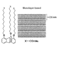
- the substituent —X—R 1 —Z present on one side of the derivative extends in the same direction of the triptycene skeleton aggregate in which the benzene rings are nested, and they are aligned. Shows the state of being accumulated. If the state which the compound 1 illustrated above accumulated is shown typically, it will become as shown in FIG. The left side of FIG. 2 shows the compound 1, and the right side schematically shows the state in which the compound 1 is accumulated in layers.
- FIG. 2 shows a state of four layers.
- the lower triptycene layer in each layer shows a triptycene skeleton aggregate in which the benzene rings are nested.
- an alkylene layer in which three same substituents are aligned and accumulated in the same direction on the upper side and an ester group is bonded to the terminal portion. Is forming.
- triptycene skeletons are accumulated, if they are randomly arranged in different directions, they do not form an orderly film as shown in FIG.
- the present inventors are the first to show that when the Janus-type triptycene derivative of the present invention is integrated, these substituents are not random, but are orderly integrated in the same direction to form a stable film.
- the headline succeeded in forming a regular and stable nano-unit film.
- a film formed by applying a solution obtained by dissolving Compound 1 exemplified above in THF (1 mg / 200 mL, about 5.3 ⁇ M) onto a glass substrate and drying the film has a single-layer structure, a two-layer structure, or a three-layer structure. It can be a structure.
- the film thickness in the case of a single layer structure was about 2.46 nm.
- the film thickness in the case of the two-layer structure was about 5.4 nm.
- the film thickness in the case of the three-layer structure was about 7.84 nm.
- a film formed by applying the same solution to a mica substrate and drying can have a single-layer structure or a double-layer structure, and the film thickness in the case of the single-layer structure is about 3.27 nm.
- the film thickness in the case of the structure was about 6.45 nm.
- the film formed by applying the same solution to the mica substrate and drying, followed by annealing at 180 ° C. had a single layer structure, and the film thickness was about 2.04 nm.
- the “functional film” in the present invention refers to a film in which functional groups having various functions are bonded to the above-described film of the present invention.
- a film such as a SAM film has a portion for binding or adsorbing to the surface of a solid substrate, a portion for obtaining van der Waals force between alkyl chains such as an alkyl chain to form a stable film, and Divided into three parts, the terminal part of the molecule.
- various functions can be imparted to the formed film by introducing a functional group having any of electrochemical, optical and biological functions into the terminal portion of the molecule.
- various functions can be imparted to the membrane of the present invention by using the terminal portion of the molecule.
- the Janus-type triptycene derivative of the present invention includes a “plane having the group —X—R 1 —Z in the general formula [I]” and a “plane of R 4 in the general formula [I]”. It is possible to introduce functional groups having various functions in the same manner as the conventional membrane on the R 4 side. Further, in the conventional film, it was essential to have a portion for binding or adsorbing to the surface of the solid substrate.
- an inter-alkyl chain such as an alkyl chain is between Since not only van der Waals force but also a toptycene skeleton portion has a film forming ability, a portion for binding or adsorbing on a solid surface is not necessarily required. Therefore, functional groups having various functions can be introduced into the group Z moiety of the Janus-type triptycene derivative represented by the general formula [I] of the present invention.
- the “solid substrate” in the present invention is a glass conventionally used as a solid substrate such as a SAM film; quartz; sapphire; nonmetal such as silicon and germanium; nonmetal oxide such as silicon oxide; gold and platinum.
- Metals such as silver and copper; metal oxides such as indium oxide and ITO (Indium Tin Oxide); GaAs; solid substrates such as CdS; organic polymer materials such as polyolefin, polyacryl, polyethersulfone, polyimide, and polyethylene terephthalate Organic substrates; not only solid substrates such as biological materials derived from animals and plants derived from collagen, starch, cellulose, etc., but also solids that are difficult to bind to and adsorb to solid substrates can be used as substrates.
- the solid shape is not particularly limited, and may be a thin film.
- the film using the Janus-type triptycene derivative of the present invention has a film-forming ability not only in the van der Waals force due to an alkyl chain but also in the triptycene skeleton portion, and therefore is necessarily bound or adsorbed on the surface of the solid substrate. This part is not essential. Therefore, it is not necessary to consider the binding property and adsorption capacity with the solid substrate, and the solid substrate is not particularly limited. However, in order to ensure the positional stability of the formed film, it is preferable to select a Janus type triptycene derivative containing a moiety that can be bound and / or adsorbed to a solid substrate.
- the “electronic device” in the present invention is a general term for electronic elements that apply the function of electrons and perform functional tasks such as amplification, data processing, and data transfer.
- Typical “electronic devices” include active elements such as transistors, diodes, thyristors, organic ELs, biosensors, and other active elements, but in some cases, passive elements such as resistors and capacitors are also included.
- the electronic device in a preferred embodiment of the present invention includes a transistor, particularly a thin film transistor, more preferably an organic field effect transistor (OFET).
- OFET organic field effect transistor
- the organic field effect transistor may be a bottom contact / top gate type, a bottom contact / bottom gate type, or a top contact / bottom gate type, but a top contact / bottom gate type is preferable.
- the “electronic element” in the present invention is a general term for electronic components using conduction of electrons in a solid, and includes an active element and a passive element. In the present invention, either an active element or a passive element is used. Usually, active elements are preferred. When the electronic device is a single electronic element, “electronic device” and “electronic element” of the present invention are used as synonyms.
- the “circuit board” in the present invention refers to a substrate in which an electronic circuit is formed on the surface of the solid substrate.
- An electronic circuit is an electrical circuit that connects electronic components with electrical conductors to create a path for current and to perform the desired operation. It amplifies the target signal and performs data processing such as calculation and control. Data can be transferred.
- the “circuit board” can be various sizes depending on the purpose. For example, it may be a circuit that performs all of data input, processing, control, output, etc., or a circuit that performs only a single purpose.
- the “electronic device” in the present invention refers to various electronic products containing at least one of the above-described electronic devices, electronic elements, or circuit boards, such as televisions; viewfinder type or monitor direct view type video tape recorders.
- the “electronic device” of the present invention may be various devices constituting the electronic product described above, and examples of such devices include display devices such as electronic paper, organic EL display, and liquid crystal display, Examples of the sensor device include various sensors.
- the “component” in the present invention refers to a portion formed of the same material, which is necessary for constituting the electronic device or the electronic element described above.
- a layer such as an insulating layer or an organic thin film layer is an example of “component”.
- “containing a component” means that the above-described electronic device or electronic element includes the “component”, that is, as a part of the above-described electronic device or electronic element. This means that a “component” exists.
- the “saturated or unsaturated divalent hydrocarbon group having 2 to 60 carbon atoms” in the present invention is a saturated or unsaturated chain having 2 to 60 carbon atoms, preferably 2 to 30, more preferably 5 to 30 carbon atoms. Or cyclic, linear or branched divalent hydrocarbon groups, and these saturated and unsaturated carbon atoms, chain carbon atoms and carbon atoms forming the ring are regular or irregular. May be arranged. Examples of the “saturated or unsaturated divalent hydrocarbon group having 2 to 60 carbon atoms” in the present invention include, for example, a straight chain having 2 to 60 carbon atoms, preferably 2 to 30 carbon atoms, more preferably 5 to 20 carbon atoms.
- a branched alkylene group a linear or branched alkenylene group having 2 to 60 carbon atoms, preferably 2 to 30 carbon atoms, more preferably 2 to 20 carbon atoms; 2 to 60 carbon atoms, preferably 2 to 30 carbon atoms, more preferably A linear or branched alkynylene group having 2 to 20 carbon atoms; containing a monocyclic, polycyclic or condensed cyclic aryl ring having 6 to 30, preferably 6 to 20, more preferably 6 to 12 carbon atoms A divalent arylene group having a total carbon number of 6 to 60, preferably 6 to 30 (the arylene group is an alkylene group, an alkenylene group, or an alkynyl group between or at the ends of the aryl ring.
- a carbon-carbon double bond for forming an alkenylene group, a carbon-carbon triple bond for forming an alkynylene group, or an aryl ring for forming an arylene group is in a saturated alkylene group (including the terminal). Alternatively, they may be regularly or irregularly arranged before and after the unsaturated carbon-carbon bond.
- C 6 , C 7 , C 8 , C 9 , C 10 , C 11 , C 12 , C 13 , C 14 , C 15 , C 16 , or C 17 linear or Branched, preferably linear alkylene groups, one, two or three carbon-carbon double bonds are regularly or irregularly arranged in the alkylene group (including the terminal)
- An alkylene group in which one, two, or three carbon-carbon triple bonds (including terminals) are regularly or irregularly arranged,-(-Ph-CH CH-) m-Ph- (
- Ph represents a p-phenylene group
- m represents an integer of 1, 2, 3, or 4.
- the “saturated or unsaturated divalent hydrocarbon group having 2 to 60 carbon atoms” in the present invention may have a substituent, and as the “substituent”, a halogen atom; a hydroxyl group; An alkyl group having 1 to 5 carbon atoms; an alkyl group having 1 to 5 carbon atoms substituted with 1 to 5, preferably 1 to 3 halogen atoms; 1 to 5, preferably Is from the group consisting of an alkoxy group having 1 to 5 carbon atoms substituted with 1 to 3 halogen atoms; an amino group; and an amino group substituted with 1 or 2 alkyl groups having 1 to 5 carbon atoms
- substituent are as follows.
- the “saturated or unsaturated divalent hydrocarbon group having 2 to 60 carbon atoms” in the present invention means that “one or more carbon atoms in the hydrocarbon group are oxygen atoms, sulfur atoms, silicon atoms” Or may be substituted with —NR 5 — (wherein R 5 represents a hydrogen atom, an alkyl group having 1 to 10 carbon atoms, or an aryl group having 6 to 30 carbon atoms) ”
- One or more carbon atoms in the chain of carbon atoms of —C—C—C— are replaced by other atoms, eg, —C—O—C—, —C—S—C—, —C—SiH 2 —C—
- the hydrogen atom bonded to the silicon atom in the formula may be substituted with a halogen atom, an alkyl group having 1 to 10 carbon atoms, or an alkoxy group having 1 to 10 carbon atoms. ), —C—NR 5 —C— and the like
- the “C 1-10 alkyl group” in the present invention is a linear or branched alkyl group having 1-10 carbon atoms, preferably 1-8 carbon atoms, more preferably 1-5 carbon atoms. Can be mentioned. Examples of such alkyl groups include, for example, methyl, ethyl, n-propyl, isopropyl, n-butyl, isobutyl, sec-butyl, tert-butyl, pentyl, hexyl, An octyl group, and the like.
- the “optionally substituted alkyl group having 1 to 5 carbon atoms” in the present invention is a straight chain having 1 to 5 carbon atoms, preferably 1 to 4 carbon atoms, more preferably 1 to 3 carbon atoms. Or a branched alkyl group is mentioned. Examples of such alkyl groups include, for example, methyl group, ethyl group, n-propyl group, isopropyl group, n-butyl group, isobutyl group, sec-butyl group, tert-butyl group, pentyl group, and the like. It is done.
- examples of the “saturated or unsaturated hydrocarbon group having 1 to 4 carbon atoms” in the present invention include an alkyl group, alkenyl group, or alkynyl group having 1 to 4 carbon atoms.
- Preferred examples of the “saturated or unsaturated hydrocarbon group having 1 to 4 carbon atoms” include linear alkyl groups having 1 to 4 carbon atoms, preferably 1 to 2 carbon atoms. Group, n-propyl group, n-butyl group and the like.
- alkenyl group having 2 to 10 carbon atoms in the present invention is a group having one or more carbon-carbon double bonds, and has a total carbon number of 2 to 10, preferably 2 to 8 carbon atoms.
- a straight chain or branched alkenyl group having 2 to 6 carbon atoms in total is used.
- alkenyl groups include vinyl, 1-methyl-vinyl, 2-methyl-vinyl, n-2-propenyl, 1,2-dimethyl-vinyl, 1-methyl-propenyl, Examples include 2-methyl-propenyl group, n-1-butenyl group, n-2-butenyl group, n-3-butenyl group and the like.
- alkynyl group having 2 to 10 carbon atoms in the present invention is a group having one or more carbon-carbon triple bonds, and has 2 to 10 carbon atoms, preferably 2 to 8 carbon atoms, more preferably Includes a straight-chain or branched alkynyl group having 2 to 6 carbon atoms in total.
- alkynyl groups include ethynyl group, n-1-propynyl group, n-2-propynyl group, n-1-butynyl group, n-2-butynyl group, n-3-butynyl group and the like. It is done.
- the “aryl group having 6 to 30 carbon atoms” in the present invention is a monocyclic, polycyclic or condensed ring having 6 to 30 carbon atoms, preferably 6 to 18 carbon atoms, more preferably 6 to 12 carbon atoms. And an aryl group of the formula.
- carbocyclic aromatic groups include a phenyl group, a naphthyl group, a biphenyl group, a phenanthryl group, and an anthryl group.
- the “5- to 8-membered heteroaryl group having 1 to 5 heteroatoms selected from the group consisting of a nitrogen atom, an oxygen atom, and a sulfur atom and having 2 to 10 carbon atoms” in the present invention is 1
- Monocyclic, polycyclic, or fused-ring heteroaryl groups having Examples of such a heterocyclic group include a 2-furyl group, a 2-thienyl group, a 2-pyrrolyl group, a 2-pyridyl group, a 2-indole group, and a benzoimidazolyl group.
- alkoxy group having 1 to 10 carbon atoms a group in which an oxygen atom is bonded to the aforementioned alkyl group having 1 to 10 carbon atoms can be mentioned.
- alkoxy groups include methoxy, ethoxy, n-propoxy, isopropoxy, butoxy, pentyloxy and the like.
- alkylthio group having 1 to 10 carbon atoms examples include a group having a sulfur atom bonded to the alkyl group having 1 to 10 carbon atoms.
- alkylthio group examples include a methylthio group, an ethylthio group, an n-propylthio group, an isopropylthio group, a butylthio group, and a pentylthio group.
- the sulfur atom in these alkylthio groups may be sulfinyl (—SO—) or sulfonyl (—SO 2 —).
- alkylcarbonyl group having 1 to 10 carbon atoms examples include those in which a carbonyl group (—CO— group) is bonded to the aforementioned alkyl group having 1 to 10 carbon atoms.
- Examples of such an alkylcarbonyl group include a methylcarbonyl group, an ethylcarbonyl group, an n-propylcarbonyl group, an isopropylcarbonyl group, and the like.
- alkoxycarbonyl group having 1 to 10 carbon atoms there may be mentioned those in which an oxycarbonyl group (—O—CO— group) is bonded to the aforementioned alkyl group having 1 to 10 carbon atoms.
- alkoxycarbonyl group examples include a methoxycarbonyl group, an ethoxycarbonyl group, an n-propoxycarbonyl group, and an isopropoxycarbonyl group.
- alkylcarbonyloxy group having 1 to 10 carbon atoms examples include those in which a carbonyloxy group (—CO—O— group) is bonded to the aforementioned alkyl group having 1 to 10 carbon atoms.
- Examples of such an alkylcarbonyloxy group include a methylcarbonyloxy group, an ethylcarbonyloxy group, an n-propylcarbonyloxy group, an isopropylcarbonyloxy group, and the like.
- the “substituent” in the various groups in the present invention is not particularly limited.
- a halogen atom, a hydroxyl group, a nitro group, a cyano group, a substituted or unsubstituted amino group an alkylsilyl group, a carbon number 1-10 alkyl group, alkenyl group having 2-10 carbon atoms, alicyclic hydrocarbon group having 3-10 carbon atoms, aryl group having 6-30 carbon atoms, arylalkyl group having 7-30 carbon atoms, heteroaryl Group, an alkylcarbonyl group having 1 to 10 carbon atoms, an alicyclic hydrocarbon-carbonyl group having 3 to 16 carbon atoms, an arylcarbonyl group having 6 to 30 carbon atoms, an arylalkylcarbonyl group having 7 to 30 carbon atoms, a carbon number
- the “monoalkyl-substituted amino group” in the present invention is an amino group in which one hydrogen atom in the amino group (—NH 2 ) is substituted with the aforementioned alkyl group having 1 to 10 carbon atoms, for example, Examples thereof include a methylamino group and an ethylamino group.
- the “dialkyl-substituted amino group” in the present invention is an amino group in which two hydrogen atoms in the amino group (—NH 2 ) are each substituted with the aforementioned alkyl group having 1 to 10 carbon atoms. Examples thereof include a dimethylamino group, a diethylamino group, and a methylethylamino group.
- the “formyl group” in the present invention is an aldehyde group (—CHO).
- Examples of the “halogen atom” in the present invention include a fluorine atom, a chlorine atom, a bromine atom, or an iodine atom.
- the “trialkylsilyl group” in the present invention is a silyl group in which three alkyl groups having 1 to 5 carbon atoms are substituted, and each alkyl group may be the same or different.
- Examples of such a trialkylsilyl group include a triethylsilyl group, an ethyldimethylsilyl group, a tert-butyldimethylsilyl group, and a tert-butyldiethylsilyl group.
- divalent linker group X of the general formula [I] of the present invention “consisting of 1 to 5 atoms selected from the group consisting of a nitrogen atom, an oxygen atom, a sulfur atom, a carbon atom, and a silicon atom, and a hydrogen atom.
- the “linker group comprising a divalent atomic group” is composed of atoms other than 1 to 5 hydrogen atoms and hydrogen atoms selected from the group consisting of a nitrogen atom, an oxygen atom, a sulfur atom, a carbon atom, and a silicon atom.
- the group consisting of a divalent atomic group is a group connecting a triptycene skeleton and a divalent hydrocarbon group R 1 group, and the structure thereof is not particularly limited.
- Preferred groups X include, for example, —O—; —S—; —SO—; —SO 2 —; —NR 6 — (wherein R 6 represents a hydrogen atom or an alkyl group having 1 to 4 carbon atoms). represents); -.
- Preferred X groups in the general formula [I] include —O—; —S—; —SO—; —SO 2 —; —NR 6 — (wherein R 6 represents a hydrogen atom or a carbon number of 1 to 4). —CH 2 —; —CH ⁇ CH—; —CO—; —OCO—; —CONR 61 — (wherein R 61 represents a hydrogen atom or an alkyl having 1 to 3 carbon atoms).
- —NR 62 CO— (wherein R 62 represents a hydrogen atom or an alkyl group having 1 to 2 carbon atoms) and the like, and particularly preferred X is —O—; —NR 6 — (wherein R 6 represents a hydrogen atom or an alkyl group having 1 to 4 carbon atoms); —CH 2 —; —CO— and the like.
- terminal group consisting of a monovalent atomic group composed of is a monovalent group that is a terminal of the divalent hydrocarbon group R 1 group in the general formula [I] of the present invention, and includes 1 to 15 There is no particular limitation as long as it is a monovalent atomic group composed of preferably 1 to 10, more preferably 1 to 6 atoms and hydrogen atoms.
- Preferred examples of the group Z include, for example, an alkyl group having 1 to 10 carbon atoms; a linear or branched alkenyl group having 2 to 15, preferably 2 to 10, more preferably 2 to 6 carbon atoms; A linear or branched alkynyl group of 15, preferably 2 to 10, more preferably 2 to 6; monocyclic, polycyclic, 6 to 15, preferably 6 to 12, more preferably 6 to 10 carbon atoms; Or a divalent aryl group having a total carbon number of 6 to 15, preferably 6 to 12, containing a condensed cyclic aryl ring (the aryl group is an alkylene group or an alkenylene between or at the end of the aryl rings) Or an alkynylene group.); A haloalkyl having 1 to 10 carbon atoms in which any position of the alkyl group having 1 to 10 carbon atoms is substituted with 1 to 7 halogen atoms ; (Wherein, R 11 represents a hydrogen atom, or an al
- COO-R 13 (wherein, R 13 is a hydrogen atom, an alkyl group, or an aryl group having a carbon number of 6 12 1 to 10 carbon atoms the expressed); -.
- OCOO-R 14 (wherein, R 14 represents an alkyl group, or an aryl group having 6 to 12 carbon atoms of 1 to 10 carbons); -.
- each R 13 independently represents a hydrogen atom, an alkyl group having 1 to 10 carbon atoms, or an aryl group having 6 to 12 carbon atoms); —NR 13 CO—R 13 (where R 13 represents Each independently represents a hydrogen atom, an alkyl group having 1 to 10 carbon atoms, or an aryl group having 6 to 12 carbon atoms.); —N (R 13 ) CON (R 13 ) 2 (where R 13 represents Each independently a hydrogen atom, carbon An alkyl group having 1 to 10 carbon atoms or an aryl group having 6 to 12 carbon atoms is represented.
- SiR 9 R 10 -N (R 13) 2 where , R 9 and R 10 may each independently be substituted with a hydrogen atom, an alkyl group having 1 to 3 carbon atoms, an alkoxy group having 1 to 3 carbon atoms, or an alkyl group having 1 to 3 carbon atoms.
- R 13 represents a hydrogen atom, an alkyl group having 1 to 10 carbon atoms, or an aryl group having 6 to 12 carbon atoms); —NH—SiR 9 R 10 —O—R 13 (wherein R 9 and R 10 are each independently an amino group optionally substituted with a hydrogen atom, an alkyl group having 1 to 3 carbon atoms, an alkoxy group having 1 to 3 carbon atoms, or an alkyl group having 1 to 3 carbon atoms. represents a group, R 13 is a hydrogen atom, a carbon 1 to 10 alkyl group, or a C6 represents the 12 aryl group); -.
- R 15 are each independently a hydrogen atom, a carbon number of 1 to 10 Represents an alkyl group or an aryl group having 6 to 12 carbon atoms; and —P ( ⁇ O) (OR 15 ) 2 (wherein R 15 each independently represents a hydrogen atom, a carbon atom having 1 to 10 carbon atoms). Represents an alkyl group or an aryl group having 6 to 12 carbon atoms.);
- the “janus type triptycene derivative” of the general formula [I] of the present invention has two different planes of the 1,8,13 position and the 4,5,16 position of the triptycene, These are triptycene derivatives having different characteristics.
- Non-Patent Document 3 a triptycene derivative is produced using a Diels-Alder reaction using benzoquinone as a key reaction. In this method, the same substituent (—OH) is present at the 13-position and the 16-position. It is difficult to produce the “Janus type triptycene derivative” of the present invention introduced at the same time.
- the inventors condense a compound in which the phenolic hydroxyl group of 1-alkoxy-6-trialkylsilyl-phenol is a leaving group such as a triflate group and 1,8-dialkoxyanthracene in the presence of a condensing agent.
- a trisubstituted triptycene derivative was successfully produced.
- a specific example of this reaction is shown in Example 1 described later. By this method, a 3-substituted triptycene derivative was able to be produced.
- triptycene derivative was a 1,8,13-3 substituted triptycene derivative (Janus type) and a 1,8,16-3 substituted Although it was a mixture of triptycene derivatives (non-Janus type) and it was difficult to separate them, 1,8,13-trimethoxytriptycene was separated and purified by recrystallization and purification. Succeeded. See Example 1 below.
- 1,8,13-Trimethoxytriptycene could be separated and purified as a crystal having a unique packing structure in which benzene rings arranged in triplicate at the triptycene site were nested.
- the crystal structure of 1,8,13-trimethoxytriptycene is shown in FIG. In FIG. 3, the oxygen atom of the methoxy group is shown in red.
- This crystal structure is an integrated structure in which dipoles are offset by a layer of triptycene molecules with the methoxy group facing the back side of the paper and a layer of molecules facing the front side of the paper. Surprisingly, such a nested crystal structure is not seen in unsubstituted triptycene.
- the 1,8,13-trimethoxytriptycene thus separated and purified can be hydrolyzed to 1,8,13-trihydroxytriptycene by a conventional method. For example, it can be hydrolyzed in the presence of boron halide in a solvent such as dichloromethane. Then, 1,8,13-trimethoxytriptycene and 1,8,13-trihydroxytriptycene obtained by hydrolysis thereof are used as key intermediates by various known synthetic means, and the present invention.
- the “Janus type triptycene derivative” can be produced. For example, a monoalkoxy derivative or a dialkoxy derivative can be obtained by alkylating with an alkylating agent.
- the remaining one or two hydroxyl groups can be further alkylated, for example, methylated or ethylated, so that the Janus triptycene derivative of the present invention having different substituents can be obtained.
- various carboxylic acids and sulfonic acids can be used as ester derivatives.
- one or two hydroxyl groups can be esterified by selecting reaction conditions.
- 1,8,13-tricyanotriptycene can be obtained by changing the hydroxyl group to triflate (Tf: trifluoromethanesulfonate) and then cyanating with dicyanozinc.
- Tf triflate
- dicyanozinc The cyano group can be hydrolyzed to formyl group or carboxyl group by an ordinary method.
- the cyano group by reducing the cyano group by a usual method, it can be converted to an aminomethyl group, and the amino group can be substituted with various substituents by a usual method.
- the obtained formyl group can be used as various reaction raw materials as a carbonyl compound.
- the formyl group can be reacted with a Wittig reagent to form a —CH ⁇ C— bond. This can be converted to a carbon-carbon triple bond by dehydrogenation by an ordinary method.
- These reactions can be performed by selecting only one or two functional groups by selecting reaction conditions.
- 1,5,16-tribromo-1,8,13-trihydroxytriptycene is obtained by brominating 1,8,13-trihydroxytriptycene using NBS (N-bromosuccinimide).
- NBS N-bromosuccinimide
- This compound is a compound having different substituents, ie, three hydroxy groups on one side and three bromo groups on the other side with respect to one symmetry plane in the triptycene molecule, and different with respect to one symmetry plane.
- This compound is a key intermediate of the “Janus type triptycene derivative” of the present invention having a functional group.
- This bromo compound can be directly converted into various aryl groups and heteroaryl groups such as phenyl and thienyl groups by various coupling reactions using boron compounds and silicon compounds.
- a functional group serving as an electron acceptor is to be introduced on the side where the bromo group is substituted, the functional group can be introduced directly or stepwise by such a coupling reaction.
- one hydroxyl group of 1,8,13-trihydroxytriptycene is methylated to form 1,8-dihydroxy-13-methoxytriptycene, and dodecyl bromide (C 12 H 25 -Br) is added thereto.
- dodecyl bromide C 12 H 25 -Br
- compound 4 1,8-didodecyloxy-13-methoxytriptycene
- Compound 4 was vacuum-deposited on a 50 nm thick silicon thin film, and its crystal state was examined by X-ray diffraction. For comparison, 1,8,13-tridodecyloxytriptycene (hereinafter referred to as “Compound 3”) was similarly vacuum deposited. In the case of Compound 4, a sharp X-ray reflection peak was obtained, but in the case of Compound 3, only a broad X-ray reflection peak was obtained. Each was annealed at 120 ° C. for 1 hour. As a result, no significant change was observed in the X-ray reflection peak of Compound 4, but a sharp X-ray reflection peak was obtained for Compound 3.
- Compound 3 1,8,13-tridodecyloxytriptycene
- the compound of the present invention has a very sharp peak without annealing, but in compound 3 having three identical substituents, the X-ray reflection peak becomes sharp only after annealing, Annealing is required. On the other hand, in compound 4 having only two large substituents of the present invention, an extremely sharp X-ray reflection peak was obtained even without annealing. Then, before and after annealing were measured change in d 001 and d 110. In Compound 4 of the present invention, by annealing, d 001 hardly changes with 2.05nm from 2.11Nm, also d 110 is 0.41nm any change was observed. On the other hand, in Compound 3 having three identical substituents, d 001 changed greatly from 2.13 nm to 2.30 nm and d 110 changed from 0.41 nm to 0.40 nm by annealing. .
- the compound represented by the general formula [I] of the present invention is a small substitution in at least one of the three substitutable positions on the 1,8,13 position plane of triptycene.
- a thin film having more regularity can be easily formed.
- the cause of this is not necessarily clear, it is considered that steric hindrance is eliminated and formation of a thin film having excellent regularity is facilitated by reducing at least one of the three locations.
- polyparaxylylene (Parylene (registered trademark)), which is one type of organic insulating material, is applied on a silicon substrate, and then an organic semiconductor DNTT (Dinaphthothienothiophene) is deposited thereon.
- DNTT Diaphthothienothiophene
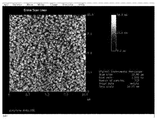
- FIG. 4 is an AMF image of DNTT without a layer of Janus-type triptycene derivative
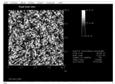
- FIG. 5 is an AMF image of DNTT when Compound 3 is used as the Janus-type triptycene derivative
- FIG. 6 is a Janus-type triptycene derivative. It is an AMF image of DNTT when using Compound 4 of the present invention.
- the crystal of DNTT is larger in the case where the layer of the Janus type triptycene derivative is provided (see FIGS. 5 and 6) than in the case of only parylene (see FIG. 4). .
- crystallization of DNTT is still larger when the compound 4 of this invention is used (refer FIG. 6). It is known that the size of the crystal grain size of DNTT has a great influence on the characteristics when this is used as a device. As a result, the characteristics of the device using the Janus-type triptycene derivative of the present invention can be improved. (See the examples below).
- the Janus type triptycene derivative represented by the general formula [I] in which the steric hindrance of the present invention has been eliminated not only has excellent film regularity but also has excellent properties in improving semiconductor characteristics. have.
- the method for producing a Janus type triptycene derivative represented by the general formula [I] of the present invention is based on the method in which 1,8,13-trimethoxytriptycene or a derivative thereof successfully separated and purified by the present inventors for the first time. As a body, it can be produced by partially replacing it.
- 1,8,13-trihydroxytriptycene which is one of derivatives of 1,8,13-trimethoxytriptycene.
- Dialkoxy-13-hydroxytriptycene is prepared, and the resulting product is then represented by the following general formula [II], Y 1 -R 1 -Z [II] (In the formula, R 1 and Z represent the aforementioned groups, and Y 1 represents a leaving group such as halogen.) It can manufacture by making it react with the compound of these. Alternatively, it may be produced by reacting 1,8,13-trihydroxytriptycene with the compound represented by the above general formula [II] and then reacting with an alkylating agent. These reactions are basically substitution reactions and can be performed according to various known substitution reactions.
- the reaction can be carried out by protecting Z with various protecting groups, and when a precursor such as a carboxyl group is to be introduced as Z. , Z can be a cyano group compound, and the resulting product can be hydrolyzed to a carboxyl group.
- Z is an ester group, the ester may be reacted as it is, or may be esterified after being converted to a carboxyl group.
- the protecting group and deprotection are well known to those skilled in the art, but if necessary, refer to Protective Group in Organic Synthesis (John Wiley and Sons, 1991) by TW Green.
- the triptycene substituent is a compound having a carbonyl group such as a formyl group, the general formula in which the group X is —C ⁇ C— can be obtained by using the Wittig reagent described above [ I].
- 1,8,13-trihydroxytriptycene is used as a raw material, and methyl 12-bromododecanoate (a chloro, iodo, or a pseudohalide such as tosylate instead of bromo) It is also possible to produce a compound having the above-mentioned ester group as a terminal group by reacting in the presence of a base.
- a solvent can be used as necessary.
- solvents include ketone solvents such as acetone and methyl ethyl ketone, ether solvents such as diethyl ether and THF, aprotic polar solvents such as DMF, DMA and DMSO, alcohol solvents such as ethanol, toluene, Aromatic hydrocarbon solvents such as xylene, halogen solvents such as dichloromethane and chlorobenzene, and the like are exemplified, but not limited thereto.
- the reaction can be performed in the presence of various reagents as necessary.
- Such a reagent is preferably a base, and examples of the base include alkali metal carbonates such as potassium carbonate, sodium carbonate and cesium carbonate, and alkali metal hydroxides such as sodium hydroxide and potassium hydroxide. It is not limited to these.
- An organic base such as trialkylamine can be used as the base, but an inorganic base is preferred.
- the reaction temperature can be arbitrarily set as long as the reaction proceeds appropriately. Usually, the range from room temperature to the boiling point of the solvent is preferable. In order to reduce the number of substituents to be introduced to one or two, the number of moles of the reagent is adjusted, the reaction time is shortened, the reaction temperature is adjusted, the amount of the solvent is increased, or a combination thereof is combined. Can be adjusted.
- the target product As a method for isolating and purifying the target product from the reaction mixture, it may be carried out by usual isolation / purification means such as solvent extraction, recrystallization, reprecipitation, silica gel column chromatography, gel filtration chromatography, etc. Can do.
- isolation / purification means such as solvent extraction, recrystallization, reprecipitation, silica gel column chromatography, gel filtration chromatography, etc. Can do.
- the product when it has optical activity, it can be optically resolved as required.
- the obtained compound into which one or two substituents are introduced may be further replaced with the following general formula [III] as necessary.
- Y 1 -R 2 [III] (In the formula, R 2 represents the aforementioned group, and Y 1 represents a leaving group such as halogen.)
- the compound represented by the general formula [I] of the present invention can be produced by performing a substitution reaction using the reagent represented by the same method as described above.
- the benzene rings arranged in triplicate in the form of three nesting rings accumulate in a nested manner, and this characteristic integration behavior is utilized.
- a two-dimensional molecular assembly with controlled dimensionality can be reasonably constructed and a film can be formed.
- the Janus type triptycene derivative represented by the general formula [I] of the present invention has its own steric hindrance eliminated, and can form a film with more regularity.
- a spin coating method, a dipping method, a casting method, an ink jet method, an ultrasonic method, a gas phase method, a vapor deposition method and the like can be arbitrarily selected. Since it can be dissolved in an organic solvent, a spin coating method, a dipping method, a casting method, an ink jet method, a vapor deposition method and the like are preferable.
- the spin coating method is a method in which a thin film having a uniform film thickness is formed by dropping a solution on a substrate that rotates at high speed.
- the dipping method is a method of forming a film by dipping a substrate in a solution.
- the cast method (including the drop cast method) is a method in which a solution is dropped on a substrate and then a solvent is dried to form a film, but the film thickness is not necessarily uniform.
- the ink jet method is a method of forming a film by dropping a minute solution at an arbitrary position.
- these known film formation methods can be used as a method for producing the film of the present invention.
- the film of the present invention exhibits a specific integration behavior, it depends on the liquid / liquid interface. It can also be performed by a film forming method.
- a solution obtained by dissolving the compound of the present invention in an organic solvent insoluble in water can be brought into contact with water to form a water / organic solvent interface, and a film can be produced at the interface.
- some of the compounds represented by the general formula [I] of the present invention can form a film by a vapor deposition method, preferably a vacuum vapor deposition method.
- a compound having a relatively low melting point and a high decomposition temperature is preferred.
- the vapor deposition method in this invention can be performed by the normal vapor deposition method.
- the compound is preferably heated to a melting point or higher to evaporate, or when the compound is sublimable, it is preferably sublimated and carried out under a reduced pressure of 10 ⁇ 5 Pa to 10 ⁇ 3 Pa.
- the temperature of the substrate may be around room temperature, but is preferably about 50 ° C. to 100 ° C.
- X is —CH 2 —
- Z is a hydrogen atom
- R 1 is an alkylene group having 8 to 15 carbon atoms, preferably Is a compound having an alkylene group of 9 to 12 carbon atoms.
- the Janus type triptycene derivative represented by the general formula [I] of the present invention used for forming the film of the present invention can be used as a purified compound as a single compound. Two or more of Janus type triptycene derivatives represented by [I] may be used in combination. Furthermore, it is also possible to use a mixture with a Janus type triptycene derivative in which the three substituents reported previously (see Patent Document 16) are the same group. This means that it is necessary to purify and separate only a single substitution product, for example, a 2-substitution product, among the substitution products generated in the first substitution reaction of 1,8,13-trimethoxytriptycene or its derivative. There is no.
- the substituted product formed by the first substitution reaction of 1,8,13-trimethoxytriptycene or a derivative thereof may be a mixture of an unsubstituted product, a 1-substituted product, a 2-substituted product, and a 3-substituted product. Even if it is such a mixture, the mixture can be used as it is as long as the characteristics of the membrane described in this specification can be maintained, and the mixture is always purified and used as a single compound. There is no need. In addition, when the amount of the 3-substituent exceeds, for example, 60%, preferably 80%, the steric hindrance due to the substituent cannot be eliminated. The described film characteristics may not be maintained.
- the above-described solid substrate of the present invention can be used. Furthermore, these solid substrates have been subjected to cleaning treatment with ultraviolet rays (UV), ozone, etc .; on these solid substrates, there are other connection terminals such as wiring and electrodes, insulation layers, conductive layers, etc.
- a laminate in which these layers are laminated can also be used as a solid substrate.
- the solid substrate used in the present invention a glass substrate or an organic substrate is preferable, and a substrate subjected to a cleaning treatment is particularly preferable.
- a step of dissolving a Janus type triptycene derivative represented by the general formula [I] of the present invention in an organic solvent to form a solution and then applying or spinning the solution.
- the method include a step of immersing a solid substrate in a coating or the solution, and a step of drying the solution on the solid substrate.
- a Janus type triptycene derivative represented by the general formula [I] of the present invention is dissolved in an organic solvent that does not intersect with a second solvent such as water to obtain a solution.
- the film thickness of the film of the present invention produced by such a method is not particularly limited, but the average thickness in the case of a monomolecular film is 0.1 nm to 5 nm, preferably 1 nm to 3 nm. Is preferred. In the case of a multilayer film, the average thickness is 2 nm to 50 nm or less, preferably 3 nm to 30 nm. Further, when the film is manufactured at the liquid / liquid interface, a film having a larger film thickness can be manufactured, and the film thickness can be 30 nm to 1000 nm, preferably 50 nm to 500 nm.
- the organic solvent for producing the membrane is not particularly limited as long as it can dissolve the Janus type triptycene derivative represented by the general formula [I] of the present invention.
- a lactone such as ⁇ -butyrolactone is used.
- Ketones such as acetone, methyl ethyl ketone, cyclohexanone, methyl-n-amyl ketone, methyl isoamyl ketone and 2-heptanone; monohydric alcohols such as methanol, ethanol and isopropanol; ethylene glycol, diethylene glycol, propylene glycol, dipropylene glycol and the like Polyhydric alcohols and derivatives thereof; glycol esters such as ethylene glycol monoacetate, diethylene glycol monoacetate, propylene glycol monoacetate, dipropylene glycol monoacetate; Monoether or monoether esters of polyhydric alcohols or the above-mentioned esters such as monomethyl ether, monoethyl ether,
- organic solvents may be used independently and may be used as 2 or more types of mixed solvents.
- Preferred organic solvents include amides such as dimethylformamide (DMF) and dimethylacetamide (DMA), cyclic ethers such as dioxane and THF, and sulfur-containing solvents such as dimethylsulfoxide (DMSO).
- Particularly preferred solvents include polar solvents such as dimethylformamide (DMF) and tetrahydrofuran (THF).
- the Janus type triptycene derivative represented by the general formula [I] of the present invention in 100 mL of an organic solvent is 0.01 mg to 1000 mg, more preferably 0.1 mg to 100 mg, still more preferably 0.1 mg. It can be 10 mg.
- the temperature at which the membrane of the present invention is produced can be usually room temperature, but depending on the type of solvent and production conditions, it can be carried out under heating or cooling.
- Drying in the production of the membrane of the present invention is sufficient by natural drying, but it can be dried by a method such as blowing dry air or nitrogen, or by heating if necessary.
- the film manufactured using an organic solvent such as methanol or chloroform, purified water, or the like may be washed, but it is not particularly necessary to wash the film.
- the film of the present invention is produced at the interface, the film produced at the interface can be transferred to a substrate such as a glass substrate and separated. The separated membrane can be dried by the method described above.
- the annealing treatment is performed on the film manufactured by the spin coating method, the dipping method, the casting method, the ink jet method, or the like of the Janus type triptycene derivative represented by the general formula [I] It is carried out by heating to about the same temperature as the melting point, preferably about 100 to 230 ° C., more preferably about 130 to 230 ° C., more preferably about 150 to 200 ° C. Further, the film produced by the vapor deposition method is performed by heating to about 100 ° C.
- the annealing treatment can be usually performed in the atmosphere, but may be performed in an inert air flow such as a nitrogen air flow.
- the annealing time is not particularly limited, but usually 5 to 50 minutes, preferably 10 to 30 minutes is sufficient.
- the film of the present invention can have a single layer structure or a bilayer structure in which the end groups Z face each other depending on the type of the end groups Z in the general formula [I]. Also, the thickness of the film can be adjusted by the manufacturing method, and it is suitable for a wide range of applications as a thin film suitable for a wide range of applications as an electronic material, an optical material, a surface treatment material, or a structure integrated with a solid substrate. A structure can be provided.
- the electronic device of the present invention can be manufactured according to the conventional method of manufacturing an electronic device, and in this case, by replacing the conventional organic thin film, particularly the SAM, with the above-described organic thin film of the present invention. Can be manufactured.
- the target organic thin film can be formed on various organic or inorganic substrates by the method described above.
- the following method can be given.
- Aluminum is deposited on the silicon wafer and patterned, and then incinerated in oxygen plasma to make the surface aluminum oxide and pattern the Al 2 O 3 / Al gate electrode whose insulating layer is aluminum oxide.
- a solution of the Janus type triptycene derivative represented by the general formula [I] of the present invention is drop-cast and dried. You may anneal at about 200 degreeC as needed. In this manner, an organic thin film containing a Janus type triptycene derivative represented by the general formula [I] of the present invention is formed on the patterned Al 2 O 3 / Al gate electrode.
- an organic semiconductor such as DNTT (dinaphthothienothiophene) is deposited on the Al 2 O 3 / Al gate electrode and the organic thin film to form an organic semiconductor layer.
- gold is deposited on the organic semiconductor layer by a vacuum deposition method or the like to form a source electrode and a drain electrode.
- a capacitor can be obtained by depositing gold directly on the organic thin film without forming the organic semiconductor layer.
- the capacitor of the present invention is characterized by having a dielectric layer composed of the organic thin film of the present invention described above between electrodes.
- the capacitor of the present invention may further contain a second dielectric of the dielectric layer.
- the second dielectric is not particularly limited as long as it is a dielectric used for a capacitor, but an organic dielectric is preferable.
- the dielectric layer is preferably a laminated structure.
- a transparent and flexible polymer substrate such as a polycarbonate substrate is washed, and then an organic conductor such as PEDOT (polyethylenedioxythiophene) or A gate electrode is formed by patterning using metal fine particles such as copper.
- an organic insulator layer such as polyimide, polymethyl methacrylate, or polyparaxylylene is formed on a part or the entire surface of the substrate.
- an organic thin film containing a Janus triptycene derivative represented by the general formula [I] of the present invention is formed so as to overlap with the gate electrode.
- an organic semiconductor such as DNTT (dinaphthothienothiophene) is deposited thereon to form an organic semiconductor layer.
- gold is deposited on the organic semiconductor layer by a vacuum deposition method or the like to form a source electrode and a drain electrode.
- Examples of the insulator in these thin film transistors include various insulators such as an inorganic material, an organic material, or an organic low molecular weight amorphous material.
- examples of inorganic materials include single metal oxides such as SiO 2 , Al 2 O 3 , Ta 2 O 5 , and ZrO 2 , composite oxides such as strontium titanate and strontium barium titanate, nitrides such as SiNx, and oxynitriding And fluoride.
- Examples of the organic material include polyimide, polymethyl methacrylate, polyparaxylylene, polyvinyl phenol, polymethyl methacrylate, polystyrene, benzocyclobutene, cyanoethyl pullulan, polyvinylidene fluoride, vinylidene-4 fluoroethylene copolymer, and Other polymer materials can be mentioned.
- Examples of the organic low molecular weight amorphous material include cholic acid and methyl cholate.
- various film forming methods such as vapor deposition, sputtering, plasma CVD (Chemical Vapor Deposition), anodization of a gate electrode, coating, adhesion from a solution, etc. are used depending on the material of the insulator. Can be adopted.
- the thickness of the gate insulating layer depends on the material, it can be about 10 nm to about 500 nm.
- Organic semiconductor materials include high molecular organic semiconductor materials such as polythiophene, polyallylamine, fluorenebithiophene copolymer, polythienylene vinylene, polyalkylthiophene, and derivatives thereof; DNTT (dinaphthothienothiophene), oligothiophene , Low molecular organic semiconductor materials such as pentacene, tetracene, copper phthalocyanine, perylene, and derivatives thereof can be used. Carbon compounds such as carbon nanotubes or fullerenes, semiconductor nanoparticle dispersions, and the like can also be used as the material for the semiconductor layer.
- organic semiconductor materials can be dissolved or dispersed in an aromatic solvent such as toluene and used as an ink-like solution or dispersion. Moreover, it can also form into a film by a vapor deposition method.
- an oxide semiconductor material for example, an oxide containing one or more elements of zinc, indium, tin, tungsten, magnesium, and gallium can be given.
- Known materials such as zinc oxide, indium oxide, indium zinc oxide, tin oxide, tungsten oxide, and zinc gallium indium oxide (In—Ga—Zn—O) can be mentioned, but the material is not limited to these materials.
- the structure of these materials may be single crystal, polycrystal, microcrystal, crystal / amorphous mixed crystal, nanocrystal scattered amorphous, or amorphous.
- a flexible plastic material such as polyethylene terephthalate (PET), polyimide, polyethersulfone (PES), polyethylene naphthalate (PEN), polymethyl methacrylate, polycarbonate; glass such as quartz
- PET polyethylene terephthalate
- PES polyethersulfone
- PEN polyethylene naphthalate
- polycarbonate glass
- quartz glass
- a substrate a silicon wafer, an aluminum wafer, and the like.
- the thin film transistor may be provided with a sealing layer, a light shielding layer, or the like as necessary.
- the material for the sealing layer can be selected from the same materials as the material for the insulator, and the light shielding layer can be a gate material or the like in which a light shielding material such as carbon black is dispersed.
- the organic thin film electronic device of the present invention can be a constituent element, whereby an electronic device with excellent stability can be obtained. That is, this invention provides the electronic device material which consists of an organic thin film formed by containing the Janus type triptycene derivative represented by general formula [I] of this invention. Also provided is a method for producing an electronic device of the present invention, characterized in that an organic thin film comprising a Janus type triptycene derivative represented by the general formula [I] of the present invention is provided in the electronic device. Will be.
- the electronic device or the electronic element of the present invention thus manufactured can be appropriately combined, and they can be wired to form an electronic circuit according to the purpose such as amplification and data processing on the substrate by a normal method.
- the electronic circuit on the substrate thus formed is the circuit board of the present invention.
- One circuit board of the present invention may be formed according to the purpose, or may be formed of two or more sheets.
- the electronic device of the present invention can be manufactured by appropriately combining such circuit boards.
- the electronic device of the present invention may itself be various electronic products, or may be a device that forms part of the electronic product, such as a display device.
- Acetonitrile 750 mL was added to 1,8-dimethoxyanthracene (22.3 g, 93.7 mmol) and cesium fluoride (CsF) (85.3 mg, 561.0 mmol) to form a suspension and heated to 80 ° C.
- CsF cesium fluoride
- 2-methoxy-6-trimethylsilyloxy-trifluoromethylsulfonate (61.5 g, 188 mmol) was added dropwise and heated to reflux for 5 hours.
- trimethoxytriptycene was composed of 2,8,13-trimethoxytriptycene (compound 5a) and 1,8,16-trimethoxytriptycene (compound 5b). 1 mixture.
- the trimethoxytriptycene mixture (10.0 mg) prepared in Preparation Example 1 was dissolved in chloroform and allowed to crystallize by standing to give the title 1,8,13-trimethoxytriptycene (2 0.0 mg) was obtained.
- this crystal is orthorhombic (orthorhombic crystal system), and the values of a, b, and c of the unit cell are angstrom units, 15.608, 13.388, and 8.041.
- the value of V was 1680 cubic angstroms.
- the structure of the obtained crystal is shown as a schematic diagram in FIG.
- Compound A IR (KBr, cm -1 ): 3382, 3062, 3022, 2961, 2936, 2836, 1597, 1479, 1455, 1381, 1317, 1269, 1159, 1088, 1065, 1020, 974, 943, 861, 791, 755 , 729, 594, 570, 469.
- the disubstituted product of the compound produced in the above production example is produced in the same manner.
- the compound 4 produced in Example 1 was prepared by setting the silicon substrate to a substrate temperature of 25 ° C. in a reduced pressure environment of 4 ⁇ 10 ⁇ 4 Pa. Heating to about 200 ° C. above the melting point, vacuum deposition was performed. The film thickness of the obtained vapor deposition film was 50 nm.
- GXD oblique incidence X-ray diffraction
- Example 2 the compound 4 produced in Example 1 was vacuum deposited on a quartz substrate, a mica substrate, a polyimide substrate, and a PET substrate, respectively. Each obtained film thickness was 50 nm.
- the molecular orientation in each of the obtained films was measured by GIXD in the same manner as in Example 2. As a result, it was found that the films were regularly oriented molecular films with a d 110 interval of about 0.41 nm.
- Comparative Example 1 Production of film by vapor deposition method using compound 3 Using a normal vacuum vapor deposition apparatus, a compound 3 produced in Production Example 15 was produced under a reduced pressure environment of 4 ⁇ 10 ⁇ 4 Pa and a substrate temperature of 25 ° C. It was heated to about 200 ° C. above its melting point and vacuum deposited. The film thickness of the obtained vapor deposition film was 50 nm. As a result of measuring the molecular orientation in the obtained film by oblique incidence X-ray diffraction (GIXD), it was found that the film was a regularly oriented molecular film having a d 110 interval of 0.41 nm. The distance of d 001 was 2.13Nm.
- GXD oblique incidence X-ray diffraction
- DNTT Denaphthothienothiophene
- a toluene solution of Compound 4 200 ⁇ M, 50 ⁇ L
- a film 5 nm
- DNTT dinaphthothienothiophene
- FIG. 6 shows a photograph of the manufactured DNTT (dinaphthothienothiophene) film measured with an atomic force microscope (AFM).
- Comparative Example 2 A DNTT film was formed in the same manner as in Example 4 except that the compound 4 film was not formed. A photograph measured with an atomic force microscope (AFM) is shown in FIG.
- Comparative Example 3 A DNTT film was formed in the same manner as in Example 4 except that the compound 3 produced in Production Example 15 was used instead of the film using Compound 4. A photograph measured with an atomic force microscope (AFM) is shown in FIG.
- FIG. 7 shows a cross-sectional structure of the created transistor.
- the transistor structure is a bottom gate, top contact type.
- a gate electrode pattern made of gold and having a thickness of 20 nm was formed on a polyimide film (Ube Industries, product number UPILEX75S) serving as a substrate.
- a 70 nm thick parylene (registered trademark, paraxylylene resin) film was formed thereon to form a gate insulating film.
- a solution of the compound 4 of the present invention was drop-cast and annealed at 120 ° C.
- DNTT Diphenyl-N-phenyl-N-phenyl-N-phenyl-N-phenyl-N-phenyl-N-phenyl-N-phenyl-N-phenyl-N-phenyl-N-phenyl-N-phenyl-N-phenyl-N-phenyl-N-phenyl-N-phenyl-N-phenyl-N-phenyl-N-phenyl-N-phenyl-N-phenyl-N-phenyl-N-phenyl-N-phenyl-N-phenyl-N-phenyl-N-phenyl-N-phenyl-N-phenyl-N-phenyl-N-phenyl-N-phenyl-N-phenyl-N-phenyl-N-phenyl-N-phenyl-N-phenyl-N-phenyl-N-phenyl-N-phenyl-N-phenyl-N-phenyl-
- Comparative Example 4 A transistor was produced in the same manner as in Example 5 except that the compound 4 film was not formed.
- the field-effect mobility (mobility) of the obtained transistor was 0.8 cm 2 / Vs, and the threshold voltage (V TH ) was ⁇ 0.5 V.
- Comparative Example 5 A transistor was produced in the same manner as in Example 5 except that Compound 3 produced in Production Example 15 was used instead of the film using Compound 4.
- the field-effect mobility (mobility) of the obtained transistor was 1.2 cm 2 / Vs, and the threshold voltage (V TH ) was ⁇ 1.9 V.
- FIG. 8 shows the results of measuring the DC bias stress resistance of the transistors of Example 5 and Comparative Example 5.
- a change in current was recorded when a DC voltage of ⁇ 8 V was applied between the drain and the source and ⁇ 8 V was applied between the gate and the source.
- FIG. 9 is a graph obtained by measuring the characteristics of the transistor of Example 5. In this measurement, a change in current was recorded when a DC voltage of ⁇ 8 V was applied between the drain and the source and a DC voltage of 0 V to ⁇ 8 V was applied between the gate and the source.
- the vertical axis on the left side of FIG. 9 indicates the drain-source current (I DS ), the vertical axis on the right side indicates the gate-source current (I GS ), and the horizontal axis indicates the gate-source voltage (V GS ).
- the transistor of Example 5 according to the present invention has the important characteristics of the transistor that the field effect mobility is high, the threshold voltage is small, and the DC bias stress resistance is high. In both cases, good results were obtained.
- the present invention can have extremely unique characteristics different from those of conventional self-assembled films, and can be applied not only as a thin film for electronic devices such as thin film transistors but also as a protective film or a biological film-like film.
- the present invention provides a thin film having a wide nano unit, a triptycene derivative useful as a novel film forming material for forming the film, and an intermediate compound for producing the same. Therefore, the present invention is useful in the industrial field using thin films such as thin film transistors, and has industrial applicability not only in the chemical industry but also in the electronic device industry.
Landscapes
- Chemical & Material Sciences (AREA)
- Organic Chemistry (AREA)
- Physics & Mathematics (AREA)
- Spectroscopy & Molecular Physics (AREA)
- Thin Film Transistor (AREA)
- Organic Low-Molecular-Weight Compounds And Preparation Thereof (AREA)
Abstract
Description
SAM膜は、ガラス基板上に有機シラン化合物を用いて形成されたことが報告され(非特許文献1参照)、また、金基板上に有機イオウ化合物を用いて形成されたことが報告されて(非特許文献2参照)から、急速に発展してきた。
SAM膜は、LB(Langmuir-Blodgett)膜よりも安定であり、気相反応によっても形成させることができ、その応用範囲は広範になってきている。また、SAM膜の膜厚は分子の大きさ(長さ)と基板との傾斜角で決定され、1nm程度の分子レベルの膜を精密にかつ簡便に製造することができる。膜厚は、一般的には、アルキル鎖の1つのメチレン単位により約0.2nmとなり、アルキル鎖の長さを調節することにより、所望の膜厚の単分子膜を正確に製造することができる。
SAM膜の形成により、固体基板の表面の特性を改質することができる。例えば、有機電界効果型トランジスタ(有機FET)では、多くの場合に絶縁層として酸化ケイ素が用いられているが、当該酸化ケイ素の表面にオクタデシルトリクロロシラン(OTS)などの有機シラン化合物によるSAM膜を形成させることにより、その表面を撥水性にすることにより、隣接する(有機)半導体の結晶性を向上させ電荷移動度を改善できるとされている。このように、固体基板の表面にSAM膜を形成させることにより、固体基板表面の親水性や疎水性を制御することができる。
例えば、アルデヒド部分を有する糖や、カルボキシル基を有する化合物を固定するために末端基としてアミノ基を有するアルキレンチオール化合物を材料としたSAM膜の形成(特許文献1参照)、末端基にシアノアリール基などの電子受容性官能基を有するアルキレンチオール化合物などを材料としたSAM膜の形成(特許文献2参照)、末端基にポリフェニレン基を有するアルキレンチオール化合物などを材料とした紫外線耐性を有するSAM膜の形成(特許文献3参照)、ビス(アダマンチルメチル)ジスルフィドを用いた剛直なアダマンタン表面膜構造を有するSAM膜の形成(特許文献4参照)、アルキレン鎖の途中に比較的長波長の光で感光する官能基を導入し、長波長の光でパターン化が可能となるリソグラフィー用のSAM膜の形成(特許文献5参照)、ピロール環拡張ポルフィリンとフラーレンを共有結合した化合物を用いた太陽電池及び光電荷分離素子用のSAM膜の形成(特許文献6参照)などが報告されている。
また、1個、2個、5個、又は6個の長鎖アルコキシ基で置換されたトリプチセン誘導体が規則的に整列しスメクチック液晶を形成することが報告されている(非特許文献3参照)が、3つの置換基が同じ方向に規則的に整列することまでは開示されていないし、SAM膜形成材料として適していることも開示されていない。
また、本発明は、下記の一般式[I]で表されるヤヌス型トリプチセン誘導体を含有してなる膜形成材料、下記の一般式[I]で表されるヤヌス型トリプチセン誘導体を用いた自己組織化膜、当該膜を表面に有する固体基板、及び当該膜の製造方法を提供する。
さらに、本発明は、絶縁体と有機半導体の極めて均一な界面を形成することで、高性能、高均質、高安定な電子デバイスを提供する。本発明の電子デバイスは、絶縁体と有機半導体の界面が極めて均一になるためにノイズレベルの低い電子デバイスを実現することで、微弱な信号、例えば生体が発する信号を高感度に検出することを可能にする。更には、本発明の界面を形成する膜はフレキシブルで大面積とすることができ、大面積でフレキシブルな電子デバイスを提供する。
しかし、トリプチセンの一方の側に3つの同じ置換基を有するトリプチセン誘導体を用いた場合には、集積構造を揃えるためにアニール処理が必要であり、アニール処理無しできれいに揃った集積構造とすることは困難であった。本発明者らは、この原因について種々検討してきたところ、同じ方向に伸びている3つの同じ置換基が、互いに立体障害を起こしており、この相互の立体障害のために、きれいに揃った集積構造とすることが困難となっているのではないかと考えた。しかし、トリプチセンの一方の側の3箇所の置換可能な位置に異なる置換基を導入することは合成化学的に困難であったが、本発明者らはこの合成に成功し、下記の一般式[I]で表されるトリプチセンの一方の側に異なる置換基を有する新規なヤヌス型トリプチセン誘導体を提供することができた。そして、当該下記の一般式[I]で表されるヤヌス型トリプチセン誘導体を用いて形成される集積構造はアニール処理なしでも、きれいに揃った集積構造を形成することができ、本発明者らの想定したとおりの結果を得ることができ、本発明を完成するに至った。
さらに、本発明者らは、これを電子デバイスの絶縁層の上に形成させることにより、当該絶縁層の材質、表面状態などに依存することなく、極めて均一で、安定性に優れた高品質の膜を形成させることができるだけでなく、同時に有機半導体などの機能を有する層を付与することもできることを見出した。
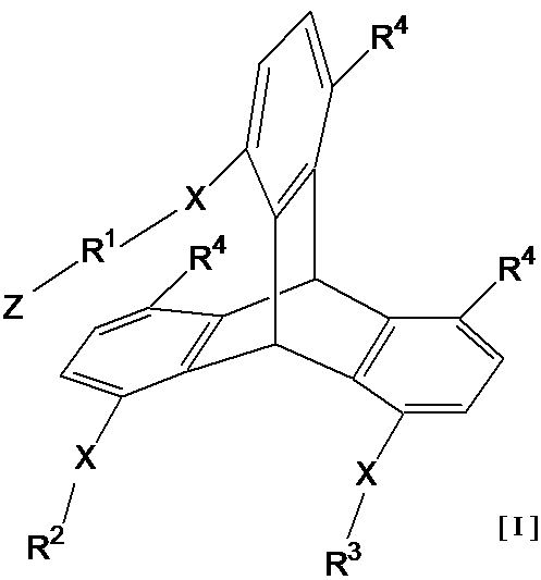
R2は、水素原子、又は炭素数1から4の飽和又は不飽和の炭化水素基を表し;
R3は、基-R1-Z、水素原子、又は炭素数1から4の飽和又は不飽和の炭化水素基を表し;
3つのR4は、同一又は異なっていてもよくそれぞれ独立して、水素原子、ハロゲン原子、水酸基、ニトロ基、シアノ基、アミノ基、モノアルキル置換アミノ基、ジアルキル置換アミノ基、置換基を有してもよい炭素数1~10のアルキル基、置換基を有してもよい炭素数2~10のアルケニル基、置換基を有してもよい炭素数2~10のアルキニル基、置換基を有してもよい炭素数1~10のアルコキシ基、置換基を有してもよい炭素数1~10のアルキルチオ基、ホルミル基、置換基を有してもよい炭素数1~10のアルキルカルボニル基、置換基を有してもよい炭素数1~10のアルコキシカルボニル基、置換基を有してもよい炭素数1~10のアルキルカルボニルオキシ基、置換基を有してもよい炭素数6~30のアリール基、又は窒素原子、酸素原子、及び硫黄原子からなる群から選ばれる1~5個のヘテロ原子を有し炭素原子を2~10個有する5~8員の置換基を有してもよいヘテロアリール基を表し;
Xは、窒素原子、酸素原子、硫黄原子、炭素原子、及びケイ素原子からなる群から選ばれる1~5個の原子及び水素原子で構成される2価の原子団からなるリンカー基を表し;
Zは、水素原子、固体基板の表面に結合若しくは吸着し得る基;又は窒素原子、酸素原子、硫黄原子、炭素原子、リン原子、ハロゲン原子、及びケイ素原子からなる群から選ばれる1~15個の原子及び水素原子で構成される1価の原子団からなる末端基を表す。)
で表されるヤヌス型トリプチセン誘導体に関する。
さらに、本発明は、前記の一般式[I]で表されるヤヌス型トリプチセン誘導体が自己組織的に整列してなる膜、特に自己組織化単分子膜、及び当該膜を固体基板の表面に有する構造体に関する。
また、本発明は、前記の一般式[I]で表されるヤヌス型トリプチセン誘導体を溶媒に溶解して溶液とし、当該溶液を固体基板の表面に塗布又は当該溶液に固体基板を浸漬し、次いで乾燥し、必要に応じてさらにアニーリングしてなる、固体基板の表面に前記の一般式[I]で表されるヤヌス型トリプチセン誘導体の膜を製造する方法に関する。
また、本発明は、前記の一般式[I]で表されるヤヌス型トリプチセン誘導体を溶媒に溶解して溶液とし、当該溶液を固体基板の表面に塗布又は当該溶液に固体基板を浸漬し、次いで乾燥し、必要に応じてさらにアニーリングしてなる、固体基板の表面に前記の一般式[I]で表されるヤヌス型トリプチセン誘導体の膜が形成された構造体を製造する方法に関する。
さらに、本発明は、前記一般式[I]で表されるヤヌス型トリプチセン誘導体を含有してなる膜を構成要素として含有してなる電子デバイスに関する。
(1)前記の一般式[I]で表されるヤヌス型トリプチセン誘導体。
(2)一般式[I]における3つのR4が、全て同じ基である、前記(1)に記載のヤヌス型トリプチセン誘導体。
(3)一般式[I]における3つのR4が、それぞれ異なる基である、前記(1)に記載のヤヌス型トリプチセン誘導体。
(4)一般式[I]におけるXが、-CH2-、-CH=CH-、-O-、又は-NR6-(ここで、R6は、水素原子、又は炭素数1~4のアルキル基を表す。)で表される2価の基である、前記(1)から(3)のいずれか一項に記載のヤヌス型トリプチセン誘導体。
(5)一般式[I]におけるXが、-CH=CH-、又は-O-で表される2価の基である、前記(4)に記載のヤヌス型トリプチセン誘導体。
(6)一般式[I]におけるR1が、炭素数2から30のアルキレン基、炭素数2から30のアルケニレン基、炭素数2から30のアルキニレン基、又は炭素数6から30のアリール環を含有してなる炭素数6から60の2価のアリーレン基である、前記(1)から(5)のいずれか一項に記載のヤヌス型トリプチセン誘導体。
(7)一般式[I]におけるR1が、炭素数2から30のアルキレン基、又は炭素数6から30のアリール環を含有してなる炭素数6から60の2価のアリーレン基である、前記(6)に記載のヤヌス型トリプチセン誘導体。
(8)一般式[I]におけるZが、水素原子、炭素数1~10のハロアルキル基、炭素数2~10のアルケニル基、炭素数2~10のアルキニル基、水酸基、-COOR7(ここで、R7は、水素原子、又は置換基を有してもよい炭素数1~5のアルキル基を表す。)、-N(R8)2(ここで、R8は、同一又は異なっていてもよい、水素原子、置換基を有してもよい炭素数1~5のアルキル基、又は置換基を有してもよい炭素数6~30のアリール基を表す。)、又は、-P(=O)(OR15)2(ここで、R15は、それぞれ独立して、水素原子、炭素数1から10のアルキル基、又は炭素数6から12のアリール基を表す。)である、前記(1)から(7)のいずれか一項に記載のヤヌス型トリプチセン誘導体。
(9)一般式[I]におけるZが、水素原子、-CF3、-CH=CH2、-C≡CH、-COOR7(ここで、R7は、水素原子、又は置換基を有してもよい炭素数1~5のアルキル基を表す。)、-NH2、又は-N(Ar1)2(ここで、Ar1は、同一又は異なっていてもよくそれぞれ独立して、置換基を有してもよい炭素数6~30のアリール基を表す。)である、前記(8)に記載のヤヌス型トリプチセン誘導体。
(10)R2が、炭素数1から4のアルキル基である、前記(1)から(9)のいずれか一項に記載のヤヌス型トリプチセン誘導体。
(11)R3が、基-R1-Z(R1及びZは前記した基を表す。)である、前記(1)から(10)のいずれか一項に記載のヤヌス型トリプチセン誘導体。
(12)R3が、炭素数1から4のアルキル基である、前記(1)から(10)のいずれか一項に記載のヤヌス型トリプチセン誘導体。
(13)一般式[I]におけるR4が、水素原子、ハロゲン原子、水酸基、ニトロ基、置換基を有してもよい炭素数1~10のアルコキシ基、又は置換基を有してもよい炭素数6~30のアリール基である、前記(1)から(12)のいずれか一項に記載のヤヌス型トリプチセン誘導体。
(14)一般式[I]におけるR4が、水素原子、ハロゲン原子、又は置換基を有してもよい炭素数1~10のアルコキシ基である、前記(13)に記載のヤヌス型トリプチセン誘導体。
(16)膜が、トリプチセン骨格の三枚羽状に配列したベンゼン環が入れ子状に集積し、かつトリプチセン骨格のベンゼン環の同じ方向に結合している3つの同じ置換基が同じ方向に整列して集積した膜である、前記(15)に記載の膜。
(17)膜が、トリプチセン骨格の三枚羽状に配列したベンゼン環が入れ子状に集積した部分、及び一般式[I]における置換基-X-R1-Zが集積した部分からなるレイヤー構造を形成している、前記(15)又は(16)に記載の膜。
(18)一般式[I]におけるZが、極性官能基である前記(15)から(17)のいずれか一項に記載の膜。
(19)極性官能基が、水酸基、アミノ基、又はカルボキシル基若しくはそのエステルである、前記(18)に記載の膜。
(20)膜が、多層膜である前記(15)から(19)のいずれか一項に記載の膜。
(21)膜が、二層膜である前記(20)に記載の膜。
(22)二層膜が、一般式[I]におけるZ基が分子間で向かい合った構造である、前記(21)に記載の膜。
(23)膜が、単分子膜である、前記(15)から(19)のいずれか一項に記載の膜。
(24)膜が、機能性膜である前記(15)から(23)のいずれか一項に記載の膜。
(25)膜が、固体基板の表面に形成されたものである、前記(15)から(24)のいずれか一項に記載の膜。
(26)前記(15)から(25)のいずれか一項に記載の膜を固体基板の表面に有する構造体。
(27)構造体が、電子デバイスの一部を形成するものである前記(26)に記載の構造体。
(28)電子デバイスが、薄膜トランジスタ(TFT)である、前記(27)に記載の構造体。
(29)固体基板が、酸化ケイ素、ガラス基板、雲母、有機基板、又は生体由来材料である、前記(26)に記載の構造体。
(31)さらに、乾燥した膜をアニーリングしてなる、前記(30)に記載の方法。
(32)溶媒が、極性溶媒である前記(30)又は(31)に記載の製造方法。
(33)極性溶媒が、ジメチルホルムアミド(DMF)、又はテトラヒドロフラン(THF)である前記(32)に記載の製造方法。
(34)一般式[I]におけるZが、極性官能基である前記(30)から(33)のいずれか一項に記載の製造方法。
(35)極性官能基が、水酸基、アミノ基、又はカルボキシル基若しくはそのエステルである、前記(34)に記載の製造方法。
(36)前記(1)から(14)のいずれか一項に記載の一般式[I]で表されるヤヌス型トリプチセン誘導体を、その融点以上に加熱して蒸発させる工程、及び蒸発した当該ヤヌス型トリプチセン誘導体を固体基板上に蒸着する工程、を含有してなる一般式[I]で表されるヤヌス型トリプチセン誘導体の膜を製造する方法。
(37)さらに、製造された膜をアニーリングする工程を含有してなる前記(36)に記載の製造方法。
(38)アニーリングが、100℃~融点までの温度で、5~50分間の加熱処理である前記(37)に記載の製造方法。
(39)蒸着が、10-5Pa~10-3Paの減圧下で行われる、前記(36)から(38)のいずれか一項に記載の製造方法。
(40)一般式[I]におけるXが-O-であり、Zが水素原子、-CH=CH2、-C≡CH、又は-CF3である、前記(36)から(39)のいずれか一項に記載の製造方法。
(41)一般式[I]におけるR1が、炭素数8~15のアルキレン基である前記(40)に記載の製造方法。
(42)一般式[I]におけるR1が、炭素数9~12のアルキレン基である前記(40)又は(41)に記載の製造方法。
(43)膜が、トリプチセン骨格の三枚羽状に配列したベンゼン環が入れ子状に集積し、かつトリプチセン骨格のベンゼン環の同じ方向に結合している置換基が同じ方向に整列して集積した膜である、前記(30)から(42)のいずれか一項に記載の製造方法。
(44)膜が、トリプチセン骨格の三枚羽状に配列したベンゼン環が入れ子状に集積した部分、及び一般式[I]における置換基-X-R1-Zが集積した部分からなるレイヤー構造を形成している、前記(30)から(43)のいずれか一項に記載の製造方法。
(45)膜が、多層膜である前記(30)から(44)のいずれか一項に記載の製造方法。
(46)膜が、二層膜である前記(45)に記載の製造方法。
(47)二層膜が、一般式[I]におけるZ基が分子間で向かい合った構造である、前記(46)に記載の製造方法。
(48)膜が、単分子膜である、前記(30)から(44)のいずれか一項に記載の製造方法。
(49)膜が、機能性膜である前記(30)から(48)のいずれか一項に記載の製造方法。
(50)固体基板が、酸化ケイ素、ガラス基板、雲母、有機基板、又は生体由来材料である、前記(30)から(49)のいずれか一項に記載の製造方法。
(52)さらに、乾燥した膜をアニーリングしてなる、前記(51)に記載の製造方法。
(53)溶媒が、極性溶媒である前記(51)又は(52)に記載の製造方法。
(54)極性溶媒が、ジメチルホルムアミド(DMF)、又はテトラヒドロフラン(THF)である前記(53)に記載の製造方法。
(55)一般式[I]におけるZが、極性官能基である前記(51)から(54)のいずれか一項に記載の製造方法。
(56)前記(1)から(14)のいずれか一項に記載の一般式[I]で表されるヤヌス型トリプチセン誘導体を、その融点以上に加熱して蒸発させる工程、及び蒸発した当該ヤヌス型トリプチセン誘導体を固体基板上に蒸着する工程、を含有してなる固体基板の表面に前記一般式[I]で表されるヤヌス型トリプチセン誘導体の膜が形成された構造体を製造する方法。
(57)さらに、製造された膜をアニーリングする工程を含有してなる前記(56)に記載の製造方法。
(58)アニーリングが、100℃~融点までの温度で、5~50分間の加熱処理である前記(57)に記載の製造方法。
(59)蒸着が、10-5Pa~10-3Paの減圧下で行われる、前記(56)から(58)のいずれか一項に記載の製造方法。
(60)一般式[I]におけるXが-O-であり、Zが水素原子、-CH=CH2、-C≡CH、又は-CF3である、前記(56)から(59)のいずれか一項に記載の製造方法。
(61)一般式[I]におけるR1が、炭素数8~15のアルキレン基である前記(60)に記載の製造方法。
(62)一般式[I]におけるR1が、炭素数9~12のアルキレン基である前記(60)又は(61)に記載の製造方法。
(63)膜が、トリプチセン骨格の三枚羽状に配列したベンゼン環が入れ子状に集積し、かつトリプチセン骨格のベンゼン環の同じ方向に結合している置換基が同じ方向に整列して集積した膜である、前記(51)から(62)のいずれか一項に記載の製造方法。
(64)膜が、トリプチセン骨格の三枚羽状に配列したベンゼン環が入れ子状に集積した部分、及び一般式[I]における置換基-X-R1-Zが集積した部分からなるレイヤー構造を形成している、前記(51)から(63)のいずれか一項に記載の製造方法。
(65)膜が、多層膜である前記(51)から(64)のいずれか一項に記載の製造方法。
(66)膜が、二層膜である前記(65)に記載の製造方法。
(67)二層膜が、一般式[I]におけるZ基が分子間で向かい合った構造である、前記(66)に記載の製造方法。
(68)膜が、単分子膜である、前記(51)から(64)のいずれか一項に記載の製造方法。
(69)膜が、機能性膜である前記(51)から(68)のいずれか一項に記載の製造方法。
(70)固体基板が、酸化ケイ素、ガラス基板、雲母、有機基板、又は生体由来材料である、前記(51)から(69)のいずれか一項に記載の製造方法。
(71)前記(1)から(14)のいずれか一項に記載のヤヌス型トリプチセン誘導体が自己組織的に整列してなる膜を構成要素として含有してなる電子デバイス。
(72)膜が、前記(15)から(25)のいずれか一項に記載の膜である、前記(71)に記載の電子デバイス。
(73)電子デバイスが、トランジスタ、コンデンサ、ダイオード、サイリスタ、電気発光素子、センサー、又はメモリーである、前記(71)又は(72)に記載の電子デバイス。
(74)電子デバイスが、トランジスタである、前記(73)に記載の電子デバイス。
(75)トランジスタが、薄膜トランジスタである前記(73)又は(74)に記載の電子デバイス。
(76)薄膜トランジスタが、基板上にゲート電極、ソース電極、ドレイン電極、及びゲート絶縁層を含む有機薄膜トランジスタである、前記(75)に記載の電子デバイス。
(77)ゲート絶縁層が、絶縁材料及び前記一般式[I]で表されるヤヌス型トリプチセン誘導体を含有してなる膜で構成されてなる、前記(76)に記載の電子デバイス。
(78)ゲート絶縁層が、絶縁材料と前記有機薄膜の積層体からなることを特徴とする、前記(77)に記載の電子デバイス。
(79)前記ゲート絶縁層の絶縁材料が、有機絶縁材料である、前記(77)又は(78)に記載の電子デバイス。
(80)有機絶縁材料が、ポリイミド、ポリメチルメタクリレート、及び/又はパリレン(登録商標)である、前記(79)に記載の電子デバイス。
(81)前記一般式[I]で表されるヤヌス型トリプチセン誘導体を含有してなる有機薄膜が、有機半導体の機能を有する基を含有するものである、前記(77)から(80)のいずれか一項に記載の電子デバイス。
(82)薄膜トランジスタが、さらに半導体からなるチャネル層を含む、前記(77)から(81)のいずれか一項に記載の電子デバイス。
(83)半導体が、有機半導体である、前記(82)に記載の電子デバイス。
(84)前記チャネル層が、有機半導体層である、前記(82)又は(83)に記載の電子デバイス。
(85)有機薄膜とチャネル層の半導体が積層している、前記(82)から(84)のいずれか一項に記載の電子デバイス。
(86)薄膜トランジスタが、ゲート絶縁層と有機半導体層との境界部が前記(15)から(25)のいずれか一項に記載の膜で構成されていることを特徴とする、前記(75)から(85)のいずれか一項に記載の電子デバイス。
(87)ゲート絶縁層、有機薄膜、及び有機半導体層が、積層構造をしている、前記(86)に記載の電子デバイス。
(88)膜が、一般式[I]で表されるトリプチセン誘導体の-X-R1-Zの側(第1の分子という)が前記絶縁体層側に、一般式[I]で表されるトリプチセン誘導体のR2の側(第2の分子という)が前記有機半導体層側に配向していることを特徴とする、前記(86)又は(87)に記載の電子デバイス。
(89)薄膜トランジスタのソース電極及び/又はドレイン電極が、前記有機薄膜と前記チャネル層との間に形成されていることを特徴とする、前記(75)から(88)のいずれか一項に記載の電子デバイス。
(90)チャネル層が、有機半導体層である、前記(89)に記載の電子デバイス。
(92)コンデンサが、電極間に前記(15)から(25)のいずれか一項に記載の膜を含有してなる誘電体層を有するコンデンサである、前記(91)に記載の電子デバイス。
(93)誘電体層が、さらに第二の誘電体を含有している、前記(92)に記載の電子デバイス。
(94)第二の誘電体が、有機誘電体である、前記(93)に記載の電子デバイス。
(95)有機薄膜と第二の誘電体が、積層構造をしている、前記(93)又は(94)に記載の電子デバイス。
(97)回路基板が、薄膜回路基板である、前記(96)に記載の回路基板。
(98)回路基板が、薄膜トランジスタが設けられた薄膜回路基板を備えているものである、前記(96)又は(97)に記載の回路基板。
(99)回路基板が、液晶表示装置や有機EL表示装置などの表示装置(いわゆるフラットパネルディスプレイ)の画素駆動用回路である、前記(96)から(98)のいずれか一項に記載の回路基板。
(101)電子機器が、電子ペーパー、有機ELディスプレイ、又は液晶ディスプレイである、前記(100)に記載の電子機器。
(102)電子機器が、心電位測定デバイス、筋電位測定デバイス、又は脳電位測定デバイス等の医療用電子機器である、前記(100)又は(101)に記載の電子機器。
(103)電子機器が、テレビ、ビューファインダ型若しくはモニタ直視型のビデオテープレコーダ、カーナビゲーション装置、ページャ、電子手帳、電卓、電子新聞、ワードプロセッサ、パーソナルコンピュータ、ワークステーション、テレビ電話、POS端末、又はタッチパネルを備えた機器等である、前記(100)又は(101)に記載の電子機器。
(105)有機薄膜が、SAMである、前記(104)に記載の有機薄膜形成用組成物。
(106)有機薄膜形成用担体が、有機溶剤である、前記(104)又は(105)に記載の有機薄膜形成用組成物。
(107)有機溶剤が、ジメチルホルムアミド(DMF)、又はテトラヒドロフラン(THF)である、前記(106)に記載の有機薄膜形成用組成物。
従来の自己組織化膜は、膜形成材料が基板の表面に結合又は吸着して集積されるものであり、基板表面に結合又は吸着される必要があったが、本発明の膜形成材料は、それ自体に集積能を有しており、基板の表面に結合又は吸着するための官能基を有することを必須としていない。また、トリプチセンはそれ自体が剛直な構造をしており、かつトリプチセン骨格の三枚羽状に配列したベンゼン環が入れ子状に集積した規則的な配列をしていることから、膜を構成する置換基がトリプチセン骨格に対して規則的に配列し、基板表面の化学的及び/又は物理的な状況にかかわらず規則的かつ剛直な膜を形成させることができる。
また、本発明の一般式[I]における基Zの種類を適宜選択することにより、固体基板表面との相互作用を強くすることもできるし、当該相互作用を弱くすることもできる。さらに、基Z同士又は基R4同士に親和性があるものを選択することにより、生体膜に類似した二層構造の膜とすることもできる。
このように、本発明の新規な膜形成材料を用いて形成される膜は、従来の自己組織化膜とは異なる極めて特異な特性を有するものとすることができ、薄膜トランジスタなどの電子デバイス用の薄膜のみならず、保護膜や生体膜類似膜などとして極めて応用範囲の広いナノ単位の薄膜を提供することができる。
また、本発明の他の態様では、半導体として機能する分子部分と絶縁体として機能する分子部分とが、一つの分子に組み込まれ、その分子が単分子膜を形成する。その単分子膜の一方の側が半導体的性質、もう一方の側が絶縁体層の積層構造を作ることができる。これにより極めて均質な半導体と絶縁体境界が形成されることになり、界面の乱れがないトランジスタを実現できる。界面の乱れが究極的に消滅することで、従来技術では得ることができない、高い移動度、高い耐久性、低いリーク電流の性能を有する半導体素子を均質で安定に作成することができる。
さらに、本発明の単分子膜の構造はトリプチセン骨格の幾何学的形状で規定されるため、得られる単分子膜は下層または上層の表面状態の影響を受けない。これにより多様な基材と組み合わせた高性能な電子デバイスを実現することができる。
「トリプチセン」自体は、既知の化合物であり、特異な三枚羽状に配列したベンゼン環を有する化合物である。本発明において、トリプチセンの位置番号はCASの命名法にしたがって次に示すとおりとする。
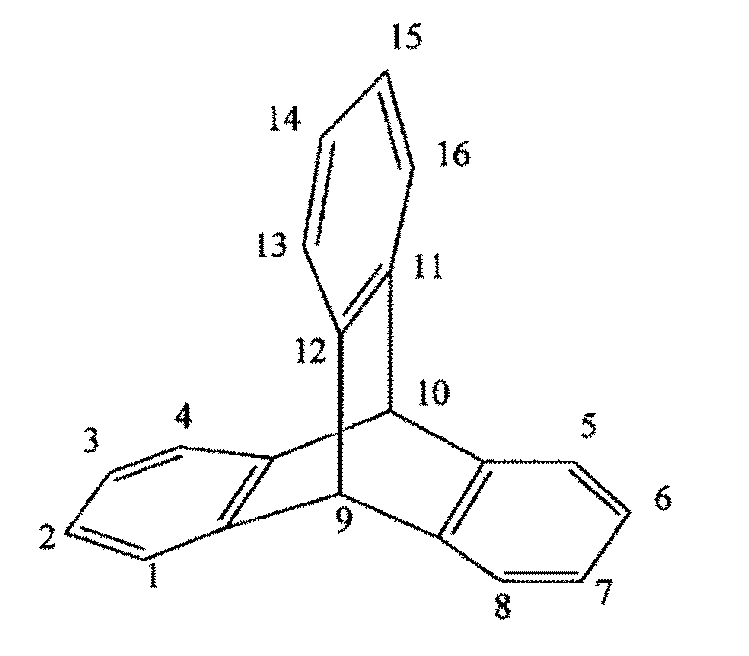
したがって、本発明のヤヌス型トリプチセン誘導体は、トリプチセンの2つの面に異なる特性を有するトリプチセン誘導体であるということができる。本発明のヤヌス型トリプチセン誘導体は、膜を形成する面と膜を形成しない面の二面を有していることを特徴とするものである。より詳細には、本発明のヤヌス型トリプチセン誘導体は、どちらかひとつだけの面、例えば1,8,13位の面だけに膜を形成するための同じ置換基を有していることを特徴とするトリプチセン誘導体である。さらに好ましい態様としては、本発明のヤヌス型トリプチセン誘導体の一般式[I]におけるR4の3つの置換基も同じ置換基であり、共通する特性を有する面として機能する態様が挙げられるが、この面の置換基は必ずしも同じである必要は無い。
本発明者らは、次式で示されるヤヌス型トリプチセン誘導体(以下、化合物1という。)を既に提供してきた(特許文献16参照)。

本発明における「トリプチセン骨格のベンゼン環の同じ方向に結合している3つの同じ置換基が同じ方向に整列して集積した」とは、本発明の一般式[I]で表されるヤヌス型トリプチセン誘導体の一方の面に存在している置換基-X-R1-Zが、前記したベンゼン環が入れ子状に集積しているトリプチセン骨格の集積体の同じ方向に伸びており、それらが整列して集積している状態を示す。
前記に例示した化合物1が集積した状態を模式的に示せば、図2に示したようになる。図2の左側は、化合物1を示し、右側は化合物1が層状に集積した状態を模式的に示している。図2の例では4層になっている状態を示している。各層における下側のトリプチセンレイヤーは、前記したベンゼン環が入れ子状に集積しているトリプチセン骨格の集積体を示している。そして、当該トリプチセンレイヤーの同じ方向、図2の化合物1の場合では上側に3つの同じ置換基が同じ方向に整列して集積して、末端部分にエステル基が結合しているアルキルレンレイヤーを形成している。
トリプチセン骨格が集積した場合に、異なる方向にランダムに整列する場合には、図2に示すような整然とした膜状にはならず、塊状となる。しかし、本発明者らは、本発明のヤヌス型トリプチセン誘導体を集積させた場合には、これらの置換基がランダムにはならず、同じ方向に整然と集積し、安定な膜を形成することを初めて見出し、規則的で安定なナノ単位の膜の形成に成功したのである。
また、このような層が重なり合って多層膜とすることもできる。この場合には、同じ方向で重なり合う場合と、相互に反対方向に向いて重なり合う場合とがある。どちらの状態になるかは、一般式[I]におけるZ基及び/又はR4基の種類や、膜形成の条件によることになる。
前記に例示した化合物1をTHFに溶解した溶液(1mg/200mL、約5.3μM)を、ガラス基板上に塗布して乾燥させて形成された膜は、一層構造、二層構造、又は三層構造とすることができる。一層構造の場合の膜厚は約2.46nmであった。二層構造の場合の膜厚は約5.4nmであった。三層構造の場合の膜厚は約7.84nmであった。また、同じ溶液を雲母基板に塗布して乾燥させて形成された膜は、一層構造、又は二層構造とすることができ、一層構造の場合の膜厚は約3.27nmであり、二層構造の場合の膜厚は約6.45nmであった。さらに、同じ溶液を雲母基板に塗布して乾燥させた後、180℃でアニーリングして形成された膜は、一層構造であり、その膜厚は約2.04nmであった。
前記してきたように、本発明のヤヌス型トリプチセン誘導体は、「一般式[I]における基-X-R1-Zを有している面」と「一般式[I]におけるR4の面」の二面を有しており、このうちのR4の面において、従来の膜と同様に種々の機能を有する官能基を導入することが可能である。また、従来の膜では、固体基板の表面に結合又は吸着するための部分を有することが必須であったが、本発明のヤヌス型トリプチセン誘導体を用いた膜では、アルキル鎖などのアルキル鎖間のvan der Waals力のみならずトプチセン骨格部分において膜形成能を有しているために、必ずしも固体表面の結合又は吸着するための部分を必須とするものではない。そのために、本発明の一般式[I]で表されるヤヌス型トリプチセン誘導体の基Z部分に、種々の機能を有する官能基を導入することも可能となる。
したがって、本発明のヤヌス型トリプチセン誘導体の膜を形成しない面、及び/又は本発明の一般式[I]で表されるヤヌス型トリプチセン誘導体の基Z部分のいずれかの部分に、各種の機能を有する官能基が導入されて形成された膜を、本発明においては「機能性膜」という。
本発明のヤヌス型トリプチセン誘導体を用いた膜は、アルキル鎖などによるvan der Waals力のみならずトリプチセン骨格部分において膜形成能を有しているために、必ずしも固体基板の表面に結合又は吸着するための部分を必須とするものではない。そのために、固体基板との結合性や吸着能を考慮する必要がなく、固体基板に特に制限はないことになる。しかしながら、形成された膜の位置安定性を確保するために、固体基板に結合及び/又は吸着することができる部分を含むヤヌス型トリプチセン誘導体を選択することが好ましい。
本発明における「電子素子」とは、固体内電子の伝導を利用した電子部品の総称であって、能動素子と受動素子があるが、本発明においては能動素子と受動素子のいずれであってもよいが、通常は能動素子が好ましい。また、電子デバイスが単一の電子素子である場合には、本発明の「電子デバイス」と「電子素子」とは同義語として使用される。
本発明における「回路基板」とは、前記した固体基板の表面に電子回路が形成されたものをいう。電子回路とは、電子部品を電気伝導体で接続し電流の通り道をつくり、目的の動作を行わせる電気回路であり、目的とする信号を増幅したり、計算や制御などのデータ処理をしたり、データを転送したりといったことができるものである。「回路基板」は、目的に応じて種々の大きさとすることができる。例えば、データの入力、処理、制御、出力などの全てを行う回路とすることもできるし、それぞれの単一の目的のみを行う回路とすることもできる。
本発明における「構成要素」とは、前記した電子デバイスや電子素子などを構成するために必要とされる、同一の材質によって形成されている部分のことをいう。例えば、絶縁層や有機薄膜層のような層が「構成要素」例として挙げられる。また、「構成要素」を含有するとは、前記した電子デバイスや電子素子などが、当該「構成要素」を内包していることを、即ち、前記した電子デバイスや電子素子などの一部として当該「構成要素」が存在していることを意味している。
より具体的には、例えば、C6、C7、C8、C9、C10、C11、C12、C13、C14、C15、C16、又はC17の、直鎖状又は分岐状、好ましくは直鎖状のアルキレン基、前記のアルキレン基の中(末端を含む)に1個、2個、又は3個の炭素-炭素二重結合が規則的又は不規則的に配置されたアルキレン基、-(-CH=CH-)n-(ここで、nは3、4、5、6、7、又は8の整数を表す。)の不飽和アルキレン基、前記のアルキレン基の中(末端を含む)に1個、2個、又は3個の炭素-炭素三重結合が規則的又は不規則的に配置されたアルキレン基、-(-Ph-CH=CH-)m-Ph-(ここで、Phは、p-フェニレン基を示し、mは1、2、3、又は4の整数を表す。)で表されるアリーレン基などが挙げられる。
本発明における「置換基を有してもよい炭素数1~5のアルキル基」としては、炭素数1~5、好ましくは炭素数1~4、より好ましくは炭素数1~3の直鎖状又は分枝状のアルキル基が挙げられる。このようなアルキル基の例としては、例えば、メチル基、エチル基、n-プロピル基、イソプロピル基、n-ブチル基、イソブチル基、sec-ブチル基、tert-ブチル基、ペンチル基、などが挙げられる。
本発明における「ジアルキル置換アミノ基」としては、アミノ基(-NH2)における2個の水素原子が、前記した炭素数1から10のアルキル基でそれぞれ置換されているアミノ基であり、例えば、ジメチルアミノ基、ジエチルアミノ基、メチルエチルアミノ基などが挙げられる。
本発明における「ハロゲン原子」としては、フッ素原子、塩素原子、臭素原子、又はヨウ素原子が挙げられる。
本発明における「トリアルキルシリル基」としては、前記した炭素数1~5のアルキル基が3個置換したシリル基であって、それぞれのアルキル基は同一であっても異なっていてもよい。このようなトリアルキルシリル基としては、トリエチルシリル基、エチルジメチルシリル基、tert-ブチルジメチルシリル基、tert-ブチルジエチルシリル基などが挙げられる。
一般式[I]における好ましいX基としては、-O-;-S-;-SO-;-SO2-;-NR6-(ここで、R6は、水素原子、又は炭素数1~4のアルキル基を表す。);-CH2-;-CH=CH-;-CO-;-OCO-;-CONR61-(ここで、R61は、水素原子、又は炭素数1~3のアルキル基を表す。);-NR62CO-(ここで、R62は、水素原子、又は炭素数1~2のアルキル基を表す。)などが挙げられ、特に好ましいXとしては、-O-;-NR6-(ここで、R6は、水素原子、又は炭素数1~4のアルキル基を表す。);-CH2-;-CO-などが挙げられる。
本発明者らは、1-アルコキシ-6-トリアルキルシリル-フェノールのフェノール性水酸基をトリフラート基などで脱離基とした化合物と、1,8-ジアルコキシアントラセンを縮合剤の存在下で縮合させることにより3置換トリプチセン誘導体を製造することに成功した。この反応の具体例を後述する実施例1に示す。この方法により、3置換トリプチセン誘導体を製造することができたが、製造された3置換トリプチセン誘導体は、1,8,13-3置換トリプチセン誘導体(ヤヌス型)と、1,8,16-3置換トリプチセン誘導体(非ヤヌス型)の混合物であり、これを分離することが困難であったが、これを再結晶して精製することにより、1,8,13-トリメトキシトリプチセンを分離精製することに成功した。後述する実施例1を参照されたい。
結晶形は斜方晶系(Orthorhombic crystal system)であり、この結晶形のa、b、及びcの値は、それぞれオングストローム単位で、15.608、13.388、8.041であった。また、Vの値は1680立方オングストロームであった。
このようにして、本発明者らはトリプチセン骨格の一つの方向に同じ置換基を有する「ヤヌス型トリプチセン誘導体」を製造することに初めて成功した。
そして、1,8,13-トリメトキシトリプチセン、及びこれを加水分解して得られる1,8,13-トリヒドロキシトリプチセンをキー中間体として、公知の各種の合成手段により、本発明の「ヤヌス型トリプチセン誘導体」を製造することができる。
例えば、アルキル化剤を用いてアルキル化することにより、モノアルコキシ誘導体、又はジアルコキシ誘導体とすることができる。残った1個又は2個の水酸基をさらにアルキル化、例えば、メチル化、エチル化することにより、置換基の異なった本発明のヤヌス型トリプチセン誘導体とすることができる。また、各種のカルボン酸やスルホン酸によりエステル誘導体とすることができる。この場合も反応条件を選択することにより1個又は2個の水酸基をエステル化することができる。さらに、水酸基をトリフラート(Tf:トリフルオロメタンスルホネート)とした後、ジシアノ亜鉛によりシアノ化することにより、1,8,13-トリシアノトリプチセンとすることができる。当該シアノ基は通常の方法により、加水分解してホルミル基又はカルボキシル基とすることができる。また、当該シアノ基を通常の方法により還元することにより、アミノメチル基とすることができ、当該アミノ基は通常の方法により各種の置換基で置換することができる。
また、得られたホルミル基はカルボニル化合物としての各種の反応原料として使用することができる。例えば、当該ホルミル基をウィッティッヒ試薬(Wittig reagent)と反応させて-CH=C-結合とすることができる。これを通常の方法により脱水素することにより炭素-炭素三重結合とすることができる。
これらの反応は、反応条件を選択することにより、1個又は2個の官能基のみを選択して反応させることができる。
このブロモ体は、ホウ素化合物やケイ素化合物を用いた各種のカップリング反応により、フェニル基やチエニル基などの各種のアリール基やヘテロアリール基に直接変換することができる。例えば、ブロモ基が置換している側に電子受容体となる機能団を導入しようとする場合には、このようなカップリング反応により直接又は段階的に当該機能団を導入することができる。

比較のために1,8,13-トリドデシルオキシトリプチセン(以下、「化合物3」という。)を同様に真空蒸着させた。
化合物4の場合にはシャープなX線反射ピークが得られたが、化合物3の場合にはブロードなX線反射ピークしか得られなかった。それぞれを、120℃で1時間、アニーリング処理した結果、化合物4のX線反射ピークに大きな変化は見られなかったが、化合物3の方はシャープなX線反射ピークが得られた。このように、本発明の化合物は、アニール処理をしなくても、極めてシャープなピークとなるが、3個の同じ置換基を有する化合物3では、アニール処理により初めてX線反射ピークがシャープとなり、アニール処理が必要となる。これに対して本発明の大きな置換基が2個しかない化合物4では、アニール処理が無くても極めてシャープなX線反射ピークが得られた。
次に、アニール処理の前後における、d001とd110の変化を測定した。
本発明の化合物4では、アニール処理により、d001は2.11nmから2.05nmとほとんど変化せず、またd110はいずれも0.41nmであり変化は見られなかった。これに対して、3個の同じ置換基を有する化合物3では、アニール処理により、d001は2.13nmから2.30nmと大きく変化し、またd110は0.41nmから0.40nmに変化した。
シリコン基板 - パリレン層 - DNTT
の場合と、
シリコン基板 - パリレン層 - ヤヌス型トリプチセン誘導体の層 - DNTT
の場合を比較した。
ヤヌス型トリプチセン誘導体として、本発明の前記した「化合物4」を用いた。また、比較のために、3個の置換基が同じドデシルオキシ基である、1,8,13-トリドデシルオキシトリプチセン(化合物3)を用いた。
それぞれの場合のDNTTの状態をAMFで観測した結果を図4、図5、及び図6に示す。図4はヤヌス型トリプチセン誘導体の層が無い場合のDNTTのAMF像であり、図5はヤヌス型トリプチセン誘導体として化合物3を用いた場合のDNTTのAMF像であり、図6はヤヌス型トリプチセン誘導体として本発明の化合物4を用いた場合のDNTTのAMF像である。
このように、本発明の立体障害が解消された一般式[I]で表されるヤヌス型トリプチセン誘導体は、膜の規則性に優れているだけでなく、半導体の特性の向上においても優れた性質を有している。
Y1-R1-Z [II]
(式中、R1及びZは前記した基を示し、Y1はハロゲンなどの脱離基を示す。)
で表されるの化合物と反応させることにより製造することができる。また、先に1,8,13-トリヒドロキシトリプチセンと前記した一般式[II]で表される化合物と反応させて、次いでアルキル化剤と反応させて製造してもよい。これらの反応は基本的には置換反応であり、公知の各種の置換反応に準じて行うことができる。
また、置換基Zが反応性である場合には、Zを各種の保護基で保護して反応を行うこともできるし、Zとしてその前駆体、例えば、カルボキシル基を導入しようとする場合には、Zとしてシアノ基の化合物を用い、得られた生成物を加水分解してカルボキシル基とすることができる。Zがエステル基の場合には、エステルのままで反応させてもよく、また、カルボキシル基とした後にエステル化してもよい。なお、保護基及び脱保護については当業者には周知であるが、必要であれば、T.W. Green著Protective Group in Organic Synthesis (John Wiley and Sons, 1991)を参照されたい。
また、トリプチセンの置換基が、ホルミル基のようなカルボニル基を有する化合物である場合には、前記したウィッティッヒ試薬(Wittig reagent)を用いることにより、基Xが-C=C-である一般式[I]の化合物とすることができる。
反応温度としては、反応が適切に進行する範囲であれば任意に設定することができるが、通常は常温から溶媒の沸点までの範囲が好ましい。
導入する置換基の数を1個又は2個にするためには、試薬のモル数を調節する、反応時間を短くする、反応温度を調節する、溶媒の量を多くする、又はこれらを組み合わせることにより調整することができる。
反応混合物から目的の生成物を単離し精製する方法としては、通常の単離・精製手段、例えば、溶媒抽出、再結晶、再沈殿、シリカゲルカラムクロマトグラフィー、ゲル濾過クロマトグラフィーなどの方法で行うことができる。また、生成物に光学活性がある場合には、必要に応じて光学分割することもできる。
Y1-R2 [III]
(式中、R2は前記した基を示し、Y1はハロゲンなどの脱離基を示す。)
で表される試薬を用いて、前記と同様な方法により、置換反応を行うことにより、本発明の一般式[I]で表される化合物を製造することができる。
スピンコート法は、高速で回転する基板の上に溶液を滴下して均一な膜厚の薄膜を成膜させる方法である。浸漬法は、溶液に基板を浸漬させて成膜する方法である。キャスト法(ドロップキャスト法を含む)は溶液を基板の上に滴下した後、溶媒を乾燥させて成膜する方法であるが、その膜厚は必ずしも均一とはならない。インクジェット法は、任意の位置に微少な溶液を滴下して成膜させる方法である。また、本発明の膜を製造する方法としては、これらの公知の成膜方法により成膜することができるが、本発明の膜は特異的な集積化挙動をすることから、液/液界面による成膜法でも行うことができる。例えば、本発明の化合物を水に溶けない有機溶媒に溶解させた溶液を、水と接触させて水/有機溶媒の界面を形成させ、当該界面において膜を製造することもできる。
また、本発明の一般式[I]で表される化合物の中のいくつかの化合物は蒸着法、好ましくは真空蒸着法により膜を形成することができる。特に、融点が比較的低く、分解温度が高い化合物が好ましい。本発明における蒸着法は、通常の蒸着法により行うことができる。例えば、化合物を融点以上に加熱して蒸発させ、又は化合物が昇華性である場合は、昇華させて、10-5Pa~10-3Paの減圧下で行われるのが好ましい。基板の温度は、室温付近でもよいが、好ましくは50℃~100℃程度が挙げられる。蒸着法による膜の形成に適した本発明の化合物としては、一般式[I]における、Xが-CH2-で、Zが水素原子で、R1が炭素数8~15のアルキレン基、好ましくは炭素数9~12のアルキレン基である化合物が挙げられる。
このことは、1,8,13-トリメトキシトリプチセン又はその誘導体の最初の置換反応で生成する置換体の中から、単一の置換体、例えば2置換体のみを、必ずしも精製分離する必要がないということである。1,8,13-トリメトキシトリプチセン又はその誘導体の最初の置換反応で生成する置換体は、無置換体、1置換体、2置換体、及び3置換体の混合物となる場合があるが、このような混合物であったとしても、本明細書で説明してきた膜の特性を維持できる範囲であれば、当該混合物をそのまま使用することができ、常に単一の化合物に精製して使用する必要は無いということである。
また、3置換体の量が、例えば、60%、好ましくは80%を超えるような状態になった場合には、置換基による立体障害を解消することができなくなり、その結果、本明細書で説明してきた膜の特性を維持できなくなることがある。このような場合には、本発明の範囲を逸脱することになるが、3置換体の量が少量であり、立体障害の解消が十分である場合には、前記で説明してきた膜の特性を維持できる範囲であり、本発明の範囲であるということになる。
本発明の膜を固体基板上に製造する方法としては、本発明の一般式[I]で表されるヤヌス型トリプチセン誘導体を有機溶媒に溶解し溶液とする工程、次いで、当該溶液を塗布若しくはスピンコート、又は当該溶液に固体基板を浸漬する工程、及び前記固体基板上の溶液を乾燥する工程を含有する方法が挙げられる。
また、本発明の膜を界面で製造する方法としては、本発明の一般式[I]で表されるヤヌス型トリプチセン誘導体を水などの第二の溶媒と交わらない有機溶媒に溶解し溶液とする工程、次いで、当該溶液に水などの第二の溶媒を加え界面を形成し、当該界面に膜を形成させる工程、製造された膜を分離する工程、及び分離された膜を乾燥する工程を含有する方法が挙げられる。
このような方法で製造された本発明の膜の膜厚としては、特に制限はないが、単分子膜とする場合の平均厚さは、0.1nmから5nm、好ましくは1nmから3nmとするのが好ましい。また、多層膜とする場合の、平均厚さは、2nmから50nm以下、好ましくは3nmから30nmとするのが好ましい。さらに、液/液界面により製造される場合には、さらに膜厚の大きな膜を製造することができ、膜厚を30nmから1000nm、好ましくは50nmから500nmとすることもできる。
好ましい有機溶媒としては、ジメチルホルムアミド(DMF)やジメチルアセトアミド(DMA)などのアミド類、ジオキサンやTHFなどの環式エーテル類、ジメチルスルホキサイド(DMSO)などの硫黄含有溶媒などが挙げられる。特に好ましい溶媒としては、ジメチルホルムアミド(DMF)、テトラヒドロフラン(THF)などの極性溶媒が挙げられる。
本発明の膜を製造する際の温度としては、通常は室温で行うことができるが、溶媒の種類や製造条件によっては、加温下又は冷却下でも行うことができる。
本発明の膜の製造における乾燥は、自然乾燥で十分であるが、乾燥した空気や窒素等を吹き付けるなどの方法や、必要により加温して乾燥させることもできる。
また、膜の形成後、メタノール、クロロホルム等の有機溶剤や精製水などを用いて製造された膜の洗浄を行ってもよいが、特に洗浄する必要はない。
本発明の膜を界面で製造する場合には、界面で製造された膜をガラス基板などの基板に転写して分離することができる。分離された膜は、前記した方法で乾燥させることができる。
また、蒸着法で製造された膜については、約100℃から200℃、好ましくは約110℃から150℃程度に加熱することにより行われる。
アニーリング処理は、通常は大気下で行うことができるが、窒素気流下などの不活性気流下であってもよい。アニーリングの時間は特に制限はないが、通常は5分から50分、好ましくは10分から30分程度で十分である。
シリコンウェハー上にアルミニウムを沈着させてパターン化し、次いで酸素プラズマ中で灰化して表面を酸化アルミニウムとして、絶縁層が酸化アルミニウムであるAl2O3/Alゲート電極をパターン化する。その上に本発明の一般式[I]で表されるヤヌス型トリプチセン誘導体の溶液をドロップキャストし、乾燥させる。必要に応じて約200℃でアニーリングしてもよい。このようにして、パターン化されたAl2O3/Alゲート電極上に本発明の一般式[I]で表されるヤヌス型トリプチセン誘導体を含有する有機薄膜を形成する。次いで、Al2O3/Alゲート電極及び有機薄膜の上にDNTT(ジナフトチエノチオフェン)などの有機半導体を沈着させて、有機半導体層を形成する。そして、有機半導体層の上に真空蒸着法などにより金を沈着させて、ソース電極とドレイン電極を形成する。
本発明のコンデンサは、電極間に前記してきた本発明の有機薄膜からなる誘電体層を有していることを特徴とするものである。本発明のコンデンサは、誘電体層のさらに第二の誘電体を含有することもできる。第二の誘電体としては、コンデンサに使用される誘電体であれば特に制限はないが、有機誘電体が好ましい。また、第二の誘電体を含有する場合には、誘電体層は積層構造とすることが好ましい。
これらの絶縁体の形成方法としては、絶縁体の材料に応じて、蒸着、スパッタリング、プラズマCVD(Chemical Vapor Deposition)、ゲート電極の陽極酸化、塗布、溶液からの付着等、種々の成膜方法を採用することができる。ゲート絶縁層の厚さは、材料にもよるが、約10nm~約500nmとすることができる。
また、本発明の一般式[I]で表されるヤヌス型トリプチセン誘導体を含有してなる有機薄膜を、電子デバイス中に設けることを特徴とする、本発明の電子デバイスを製造する方法が提供されることになる。
トリメトキシトリプチセン混合物の製造
次に示す反応式に沿ってトリメトキシトリプチセンを製造した。

1H-NMR(400MHz、CDCl3): δ (ppm)
7.01 (d, J = 0.7 Hz, 3H), 6.90 (dd, J = 7.3, 1.0 Hz, 3H), 6.80 (s, 1H), 6.58 (dd, J = 8.2, 0.7 Hz, 3H), 5.38 (s, 1H), 3.86 (s, 9H).
化合物5b:
1H-NMR(400MHz、CDCl3):δ (ppm)
7.09-7.07 (d, J = 7.2 Hz, 1H), 7.06-7.04 (d, J = 7.2 Hz, 2H), 6.93-6.89 (t, J = 7.8 Hz, 1H), 6.93-6.89 (t, J = 7.7 Hz, 2H), 6.58-6.56 (d, J = 7.7 Hz, 2H), 6.56-6.54 (d, J = 7.8 Hz, 2H), 6.35 (s, 1H), 5.87 (s, 1H), 3.84 (s, 6H), 3.83 (s, 3H).
1,8,13-トリメトキシトリプチセン(化合物5a)単結晶の製造

得られた結晶の単結晶X線構造解析を行った結果、この結晶は、斜方晶系(Orthorhombic crystal system)であり、単位格子のa、b、及びcの値は、それぞれオングストローム単位で、15.608、13.388、8.041であった。また、Vの値は1680立方オングストロームであった。
得られた結晶の構造を図3に模式図として示す。
1,8,13-トリヒドロキシトリプチセン(化合物6)の製造
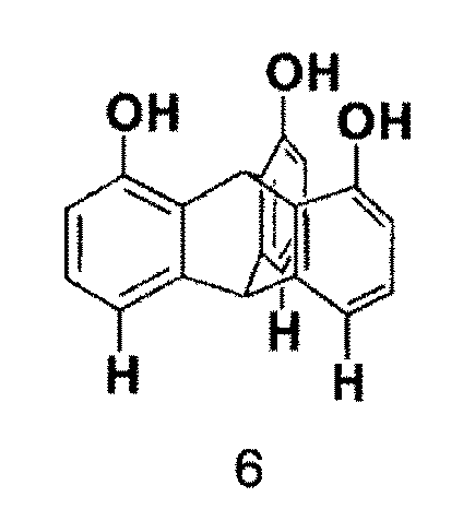
1H-NMR(400MHz、アセトン-d6):δ (ppm)
8.35 (br, s, 3H), 6.94-6.93 (d, J = 7.2 Hz, 3H), 6.86 (s, 1H), 6.79-6.75 (dd, J = 7.2, 0.9 Hz, 3H), 6.56-6.54 (dd, J = 8.1, 0.9 Hz, 3H), 5.44 (s, 1H).
1,8,13-トリヒドロキシ-4,5,16-トリブロム-トリプチセン(化合物7)の製造
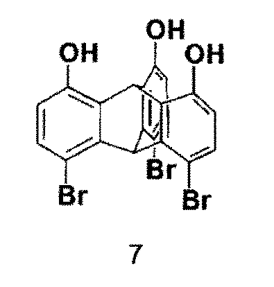
1H-NMR(400MHz、CDCl3):δ (ppm)
7.08-7.06 (d, J = 8.7 Hz, 3H), 6.96 (s, 1H), 6.82 (s, 1H), 6.63-6.61 (d, J = 8.7 Hz, 3H).
1,8,13-トリス(tert-ブチルジメチルシリルオキシ)-4,5,16-トリブロモトリプチセン(化合物8)の製造
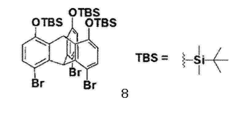
1H-NMR(400MHz、CDCl3):δ (ppm)
7.04 (d, J = 8.4 Hz, 3H), 6.83 (s, 1H), 6.55 (s, 1H), 6.46 (d, J = 8.4 Hz, 3H), 0.97 (s, 27H), 0.25 (s, 18H).
1,8,13-トリス(tert-ブチルジメチルシリルオキシ)-4,5,16-トリホルミルトリプチセン(化合物9)の製造
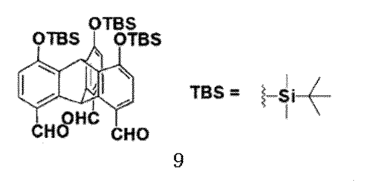
1H-NMR(400MHz、CDCl3):δ (ppm)
10.4 (s, 3H), 9.28 (s, 1H), 7.44 (d, J = 8.6 Hz, 3H), 6.75 (s, 1H), 6.71 (d, J = 8.6 Hz, 3H), 0.99 (s, 27H), 0.34 (s, 18H).
1,8,13-トリス(tert-ブチルジメチルシリルオキシ)-4,5,16-トリス(2,2-ジブロモビニル)-トリプチセン(化合物10)の製造
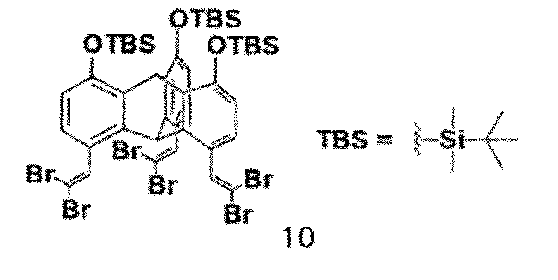
1H-NMR(400MHz、CDCl3):δ (ppm)
7.26 (s, 1H), 6.99 (d, J = 8.7 Hz, 3H), 6.60 (s, 1H), 6.56 (d, J = 8.7 Hz, 3H), 5.70 (s, 1H), 1.01 (s, 27H), 0.30 (s, 18H).
1,8,13-トリス(tert-ブチルジメチルシリルオキシ)-4,5,16-トリエチニルトリプチセン(化合物11)の製造

1H-NMR(400MHz、CDCl3):δ (ppm)
7.10 (s, 1H), 7.02 (d, J = 8.7 Hz, 3H), 6.54 (s, 1H), 6.50 (d, J = 8.7 Hz, 3H), 3.26 (s, 3H), 0.97 (s, 27H), 0.25 (s, 18H).
1,8,13-トリ(トリフルオロメチルスルホニルオキシ)トリプチセン(化合物12)の製造

1H-NMR(400MHz、アセトン-d6):δ (ppm)
7.77 (d, J = 7.4 Hz, 3H), 7.39 (t, J = 8.1 Hz, 3H), 7.27 (d, J = 8.6 Hz, 3H), 6.58 (s, 1H), 6.31 (s, 1H).
1,8,13-トリシアノトリプチセン(化合物13)の製造

1H-NMR(400MHz、アセトン-d6):δ (ppm)
7.95 (d, J = 7.3 Hz, 3H), 7.60 (d, J = 8.6 Hz, 3H), 7.40 (t, J = 8.1 Hz, 3H), 6.77 (s, 1H), 6.26 (s, 1H).
次に示す化合物1の製造
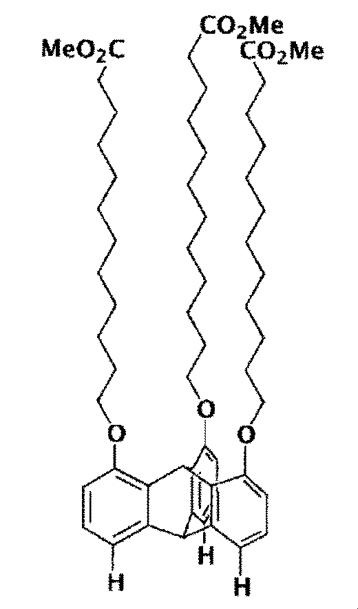
1H-NMR(400MHz、CDCl3):δ(ppm)
6.99 (d, J = 7.3 Hz, 3H), 6.89-6.84 (m, 4H), 6.54 (d, J = 8.3 Hz, 3H), 5.37 (s, 1H), 3.96 (t, J = 6.6 Hz, 6H), 3.67 (s, 9H), 1.85 (m, 6H), 1.705-1.270 (m, 60H).
次に示す化合物2の製造

1H-NMR(400MHz、DMSO-d6):δ(ppm)
11.95 (s, 3H), 7.02 (d, J = 7.6 Hz, 3H), 6.89 (t, J = 7.6 Hz, 3H), 6.67(s, 1H), 6.63 (d, J = 7.6 Hz, 3H), 5.53 (s, 1H), 3.92 (t, J = 6.4 Hz, 6H), 2.17 (t, J = 7.5 Hz, 6H), 1.78-1.26 (m, 60H).
次に示す化合物14の製造
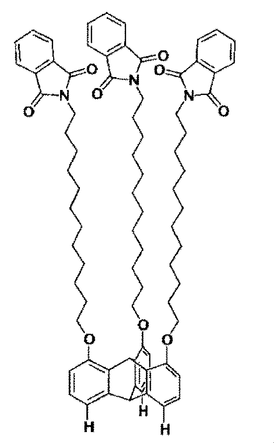
1H-NMR(400MHz、CDCl3):δ(ppm)
7.82 (m, 6H), 7.68 (m, 6H), 6.98 (d, J = 7.2 Hz, 3H), 6.89 (s, 1H), 6.88 (t, J = 8.1 Hz, 3H), 6.53 (d, J = 8.1 Hz, 3H), 5.36 (s, 1H), 3.95 (t, J = 6.4 Hz, 3H), 3.66 (t, J = 7.3 Hz, 3H), 1.8-1.2 (m, 60 H).
次に示す化合物15の製造
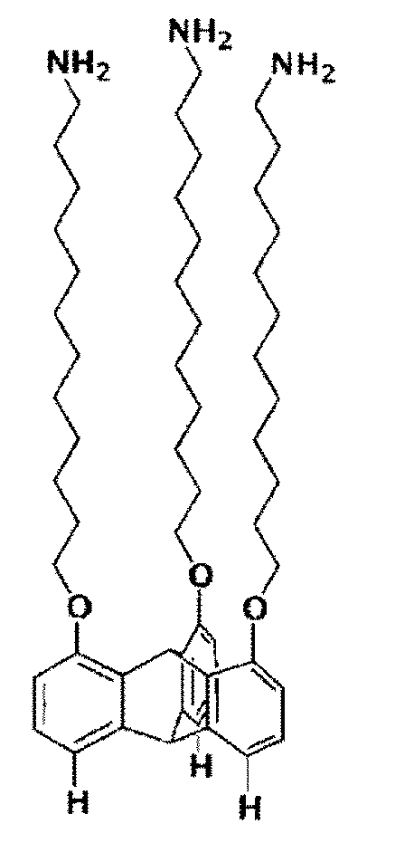
1H-NMR(400MHz、DMSO-d6):δ(ppm)
7.05 (d, J = 7.6 Hz, 3H), 6.91 (t, 7.6 Hz, 3H), 6.81 (s, 1H), 6.66 (d, J = 7.6 Hz, 3H), 5.53 (s, 1H), 4.00 (t, J = 6.4 Hz, 6H), 2.67 (t, J = 7.5 Hz, 6H), 1.81 (m, 6H), 1.59 (m, 6H), 1.47-1.29 (m, 48H).
次に示す化合物3の製造
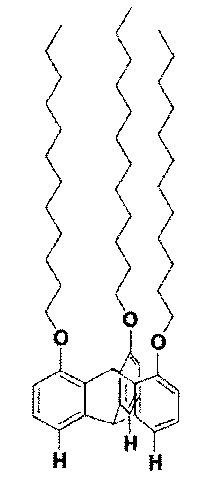
1H-NMR(400MHz、アセトン-d6):δ(ppm)
7.99 (d, J = 7.2 Hz, 3H), 7.91 (s, 1H), 7.89 (t, J = 7.6 Hz, 3H), 7.55 (d, J = 8.1 Hz, 3H), 3.95 (t, J = 6.4 Hz, 6H), 1.85 (q, J = 7.1 Hz, 6H), 1.60-1.55 (m, 6H), 1.36-1.28 (m, 54H), 0.89 (t, J = 6.8 Hz, 9H).
次に示す化合物16の製造

1H-NMR(400MHz、アセトン-d6):δ(ppm)
6.99 (d, J = 7.2 Hz, 3H), 6.89 (s, 1H), 6.87 (t, J = 7.8 Hz, 3H), 6.54 (d, J = 7.8 Hz, 3H), 5.37 (s, 1H), 3.96 (t, J = 6.4 Hz, 6H), 2.19 (td, J = 7.1 Hz, J = 2.6 Hz, 6H), 1.94 (t, J = 2.6 Hz, 3H), 1.85 (q, J = 7.0 Hz, 6H), 1.58-1.50 (m, 12H), 1.41 -1.35 (m, 24H).
次に示す化合物17の製造

1H-NMR(300MHz、アセトン-d6):δ(ppm)
7.00 (d, J = 7.2 Hz, 3H), 6.90 (s, 1H), 6.87 (t, J = 7.8 Hz, 3H), 6.55 (d, J = 7.5 Hz, 3H), 5.87-5.75 (m, 3H), 5.04-4.92 (m, 6H), 5.37 (s, 1H), 3.96 (d, J = 6.6 Hz, 6H), 2.08-2.01 (m, 6H), 1.85 (q, J = 6.6 Hz, 6H), 1.65-1.51 (m, 12H), 1.36-1.32 (m, 24H).
次に示す化合物18の製造


1H-NMR(400MHz、CDCl3):δ(ppm)
7.00 (d, 3H, J = 7.4 Hz), 6.89 (s, 1H), 6.87 (dd, 3H, J = 7.4, 7.4 Hz), 6.55 (d, 3H J = 7.4 Hz), 5.37 (s, 1H), 3.96 (t, 6H, J = 6.5 Hz), 1.85(m, 6H), 1.61-1.51 (tt, 6H, J = 6.5, 6.5 Hz), 1.43-1.29 (m, 36H).
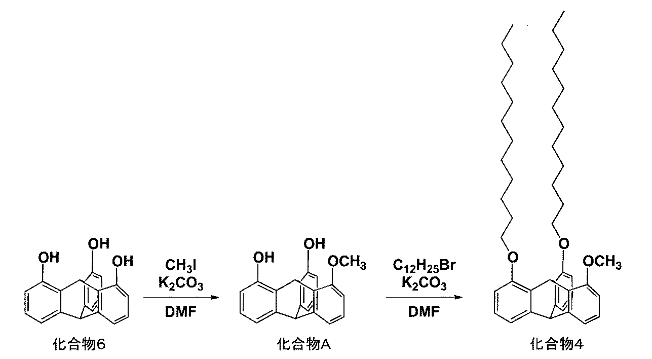
製造例3で製造した化合物6(500mg, 1.65mmol)及び炭酸カリウム(342mg, 2.48mmol)のジメチルホルムアミド(DMF)懸濁液(10.0mL)に対してヨードメタン(351mg, 2.47mmol)を混合し、75℃で12時間撹拌した。反応混合物を室温まで冷却し、ジエチルエーテル500mLを加え、水300mLで二回、塩化ナトリウム飽和水溶液で一回洗浄した。有機層を硫酸マグネシウムで乾燥し、濾過した後、ろ液を減圧留去した。残渣をクロロホルム/アセトン(7:3, v/v)を溶離液とするシリカゲルカラムクロマトグラフィーに供し、化合物Aを収率48%で白色固体として得た(251mg, 0.792mmol)。
IR (KBr, cm-1): 3382, 3062, 3022, 2961, 2936, 2836, 1597, 1479, 1455, 1381, 1317, 1269, 1159, 1088, 1065, 1020, 974, 943, 861, 791, 755, 729, 594, 570, 469.
1H-NMR(400MHz、acetone-d6): δ (ppm)
8.30 (s, 2H), 7.05 (d, J = 7.3 Hz, 1H),6.95 (d, J = 7.5 Hz, 2H), 6.94 (t, J = 7.5 Hz, 1H), 6.88 (s, 1H), 6.77 (t, J = 7.3 Hz, 2H), 6.66 (d, J = 7.4 Hz, 1H), 6.55 (d, J = 8.1 Hz, 2H), 5.48 (s, 1H), 3.83 (s, 3H).
APCI-TOF MS: calcd. for C21H16O3 として、[M]+: m/z 計算値: 316.11,
実測値: 316.11.
化合物A(250mg, 0.788mmol)と炭酸カリウム(653mg, 4.73mmol)のDMF懸濁液(5.0mL)に対し、1-ブロモドデカン(1.18g, 4.73mmol)を混合し、75℃で12時間撹拌した。反応混合物を室温まで冷却し、ジエチルエーテル500mLを加え、水300mLで二回、塩化ナトリウム飽和水溶液で一回洗浄した。有機層を硫酸マグネシウムで乾燥し、濾過した後、ろ液を減圧留去した。残渣を、クロロホルムを溶離液とするシリカゲルカラムクロマトグラフィーに供し、化合物4を収率82%で白色固体として得た(421mg, 0.646mmol)。
IR (KBr, cm-1): 3855, 3435, 2922, 2853, 1598, 1485, 1467, 1439, 1396, 1324, 1283, 1198, 1104, 1065, 855, 787, 731, 642, 607, 593.
1H-NMR(400MHz、CDCl3): δ (ppm)
7.00 (d, J = 7.1 Hz, 1H), 6.99 (d, J = 7.2 Hz, 2H), 6.89 (t, J = 7.4 Hz, 1H), 6.89 (s, 1H), 6.87 (t, J = 7.3 Hz, 2H), 6.57 (d, J = 7.3 Hz, 1H), 6.56 (d, J = 7.5 Hz, 2H), 5.37 (s, 1H), 4.02~3.92 (m, 4H). 3.84 (s, 3H), 1.91-1.79 (m, 4H), 1.65-1.50 (m, 4H), 1.44-1.24 (m, 35H), 0.89 (t, J = 6.8 Hz, 6H).
APCI-TOF MS: calcd. for C45H64O3 として、[M]+: m/z 計算値: 652.49,
実測値: 652.49.
通常の真空蒸着装置を用いて、4×10⁻⁴Paの減圧環境下で、シリコン基板を基板温度25℃として、実施例1で製造した化合物4を融点以上の約200℃に加熱して、真空蒸着した。得られた蒸着膜の膜厚は50nmであった。
得られた膜における分子の配向を斜入射X線回折法(GIXD)で測定した結果、d110の間隔が0.41nmの規則的な配向分子膜であることがわかった。また、d001の間隔は2.11nmであった。この結果からも配向分子膜におけるトリプチセン骨格の間隔が0.81nmであることがわかった。
前記の方法でシリコン基板上に形成された膜を120℃で60分間アニールした。得られた膜における分子の配向を斜入射X線回折法(GIXD)で測定した結果、d110の間隔は0.41nmであり、変化は見られなかった。また、d001の間隔は2.05nmであり、大きな変化は見られなかった。
得られたそれぞれの膜における分子の配向を、実施例2と同様にGIXDで測定した結果、d110の間隔が約0.41nmの規則的な配向分子膜であることがわかった。
化合物3を用いた蒸着法による膜の製造
通常の真空蒸着装置を用いて、4×10⁻⁴Paの減圧環境下で、シリコン基板を基板温度25℃として、製造例15で製造した化合物3を融点以上の約200℃に加熱して、真空蒸着した。得られた蒸着膜の膜厚は50nmであった。
得られた膜における分子の配向を斜入射X線回折法(GIXD)で測定した結果、d110の間隔が0.41nmの規則的な配向分子膜であることがわかった。また、d001の間隔は2.13nmであった。この結果からも配向分子膜におけるトリプチセン骨格の間隔が0.81nmであることがわかった。
前記の方法でシリコン基板上に形成された膜を120℃で60分間アニールした。得られた膜における分子の配向を斜入射X線回折法(GIXD)で測定した結果、d110の間隔は0.40nmであり、d001の間隔は2.30nmであり、大きな変化が見られた。
パリレン(登録商標、パラキシリレン系樹脂)膜の上に、化合物4のトルエン溶液(200μM,50μL)をドロップキャストし、およそ2分子層からなる膜(5nm)を形成した。
これを自然乾燥させ、その上にDNTT(ジナフトチエノチオフェン)を真空蒸着法で約30nmの厚さに形成した。製造されたDNTT(ジナフトチエノチオフェン)の膜を 原子間力顕微鏡(AFM)で測定した写真を図6に示す。
化合物4の膜を形成させなかった他は実施例4と同様にして、DNTT膜を形成した。
原子間力顕微鏡(AFM)で測定した写真を図4に示す。
化合物4を用いた膜の代わりに、製造例15で製造した化合物3を用いた他は実施例4と同様にして、DNTT膜を形成した。
原子間力顕微鏡(AFM)で測定した写真を図5に示す。
図7に作成したトランジスタの断面構造を示す。トランジスタ構造はボトムゲート、トップコンタクト型である。初めに、基板となるポリイミドフィルム(宇部興産、品番UPILEX75S)上に厚さ20nmで金からなるゲート電極パターンを形成した。その上に厚さ70nmのパリレン(登録商標、パラキシリレン系樹脂)膜を形成してゲート絶縁膜とした。そのさらに上に本発明の化合物4の溶液をドロップキャストし、120℃で1時間アニーリングして、厚さ5nmの多層分子膜を製造した。この化合物4からなる膜の上にDNTT(ジナフトチエノチオフェン)を厚さ30nmでパターン化し、その上に金電極を付けた。
得られたトランジスタの電界効果移動度(モビリティー)は1.5cm2/Vsであり、スレショルド電圧(VTH)は-0.2Vであった。
化合物4の膜を形成させなかった他は実施例5と同様にして、トランジスタを製造した。
得られたトランジスタの電界効果移動度(モビリティー)は0.8cm2/Vsであり、スレショルド電圧(VTH)は-0.5Vであった。
化合物4を用いた膜の代わりに、製造例15で製造した化合物3を用いた他は実施例5と同様にして、トランジスタを製造した。
得られたトランジスタの電界効果移動度(モビリティー)は1.2cm2/Vsであり、スレショルド電圧(VTH)は-1.9Vであった。
図9は、実施例5のトランジスタの特性を測定したグラフである。この測定では、ドレイン-ソース間に-8V、ゲート-ソース間に0Vから-8Vまでの直流電圧を印加した時の電流変化を記録した。図9の左側の縦軸はドレイン-ソース電流(IDS)を示し、右側縦軸はゲート-ソース電流(IGS)を示し、横軸はゲート-ソース電圧(VGS)を示す。
したがって、本発明は、薄膜トランジスタなどの薄膜を利用する産業分野において有用であり、化学産業のみならず電子素子産業などにおいて産業上の利用可能性を有している。
Claims (24)
- 次の一般式[I]
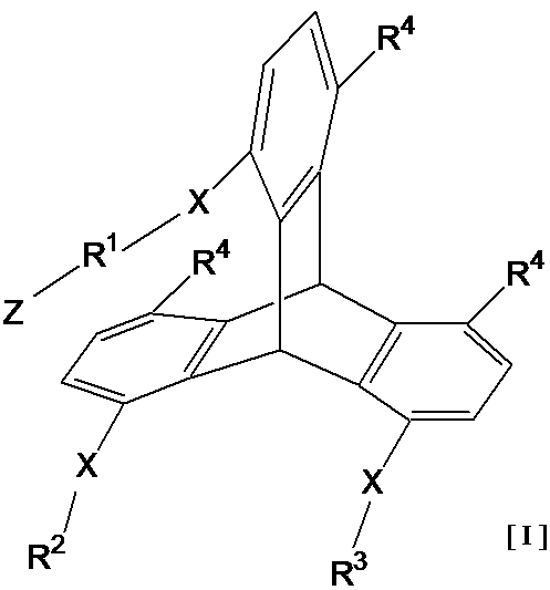
R2は、水素原子、又は炭素数1から4の飽和又は不飽和の炭化水素基を表し;
R3は、基-R1-Z、水素原子、又は炭素数1から4の飽和又は不飽和の炭化水素基を表し;
3つのR4は、同一又は異なっていてもよくそれぞれ独立して、水素原子、ハロゲン原子、水酸基、ニトロ基、シアノ基、アミノ基、モノアルキル置換アミノ基、ジアルキル置換アミノ基、置換基を有してもよい炭素数1~10のアルキル基、置換基を有してもよい炭素数2~10のアルケニル基、置換基を有してもよい炭素数2~10のアルキニル基、置換基を有してもよい炭素数1~10のアルコキシ基、置換基を有してもよい炭素数1~10のアルキルチオ基、ホルミル基、置換基を有してもよい炭素数1~10のアルキルカルボニル基、置換基を有してもよい炭素数1~10のアルコキシカルボニル基、置換基を有してもよい炭素数1~10のアルキルカルボニルオキシ基、置換基を有してもよい炭素数6~30のアリール基、又は窒素原子、酸素原子、及び硫黄原子からなる群から選ばれる1~5個のヘテロ原子を有し炭素原子を2~10個有する5~8員の置換基を有してもよいヘテロアリール基を表し;
Xは、窒素原子、酸素原子、硫黄原子、炭素原子、及びケイ素原子からなる群から選ばれる1~5個の原子及び水素原子で構成される2価の原子団からなるリンカー基を表し;
Zは、水素原子、固体基板の表面に結合若しくは吸着し得る基;又は窒素原子、酸素原子、硫黄原子、炭素原子、リン原子、ハロゲン原子、及びケイ素原子からなる群から選ばれる1~15個の原子及び水素原子で構成される1価の原子団からなる末端基を表す。)
で表されるヤヌス型トリプチセン誘導体。 - 一般式[I]におけるXが、-CH2-、-CH=CH-、-O-、又は-NR6-(ここで、R6は、水素原子、又は炭素数1~4のアルキル基を表す。)で表される2価の基である、請求項1に記載のヤヌス型トリプチセン誘導体。
- 一般式[I]におけるR1が、炭素数2から30のアルキレン基、炭素数2から30のアルケニレン基、炭素数2から30のアルキニレン基、炭素数6から30のアリール環を含有してなる炭素数6から60の2価のアリーレン基である、請求項1又は2に記載のヤヌス型トリプチセン誘導体。
- 一般式[I]におけるZが、水素原子、炭素数1~10のハロアルキル基、炭素数2~10のアルケニル基、炭素数2~10のアルキニル基、水酸基、-COOR7(ここで、R7は、水素原子、又は置換基を有してもよい炭素数1~5のアルキル基を表す。)、-N(R8)2(ここで、R8は、同一又は異なっていてもよい、水素原子、置換基を有してもよい炭素数1~5のアルキル基、又は置換基を有してもよい炭素数6~30のアリール基を表す。)、又は、-P(=O)(OR15)2(ここで、R15は、それぞれ独立して、水素原子、炭素数1から10のアルキル基、又は炭素数6から12のアリール基を表す。)である、請求項1から3のいずれか一項に記載のヤヌス型トリプチセン誘導体。
- 一般式[I]におけるR4が、水素原子、ハロゲン原子、水酸基、ニトロ基、置換基を有してもよい炭素数1~10のアルコキシ基、又は置換基を有してもよい炭素数6~30のアリール基である、請求項1から4のいずれか一項に記載のヤヌス型トリプチセン誘導体。
- R2が、炭素数1から4のアルキル基である、請求項1から5のいずれか一項に記載のヤヌス型トリプチセン誘導体。
- R3が、基-R1-Z(R1及びZは前記した基を表す。)である、請求項1から6のいずれか一項に記載のヤヌス型トリプチセン誘導体。
- 請求項1から7のいずれかに記載のヤヌス型トリプチセン誘導体が、自己組織的に整列してなる膜。
- 膜が、トリプチセン骨格の三枚羽状に配列したベンゼン環が入れ子状に集積し、かつトリプチセン骨格のベンゼン環の同じ方向に結合している置換基が同じ方向に整列して集積した膜である、請求項8に記載の膜。
- 膜が、多層膜である、請求項8又は9に記載の膜。
- 膜が、単分子膜である、請求項8又は9に記載の膜。
- 請求項8から11のいずれか一項に記載の膜を固体基板の表面に有する構造体。
- 構造体が、電子デバイスの一部を形成するものである、請求項12に記載の構造体。
- 電子デバイスが、薄膜トランジスタ(TFT)である、請求項13に記載の構造体。
- 請求項1から7のいずれか一項に記載のヤヌス型トリプチセン誘導体を溶媒に溶解し、当該溶液を固体基板の表面に塗布するか又は当該溶液に固体基板を浸漬し、次いで乾燥してなる、ヤヌス型トリプチセン誘導体の膜を製造する方法。
- さらに、乾燥した膜をアニーリングしてなる、請求項15に記載の製造方法。
- 溶媒が、極性溶媒である、請求項15又は16に記載の製造方法。
- 膜が、トリプチセン骨格の三枚羽状に配列したベンゼン環が入れ子状に集積し、かつトリプチセン骨格のベンゼン環の同じ方向に結合している置換基が同じ方向に整列して集積した膜である、請求項15から17のいずれか一項に記載の製造方法。
- 膜が、多層膜である、請求項15から18のいずれか一項に記載の製造方法。
- 膜が、単分子膜である、請求項15から18のいずれか一項に記載の製造方法。
- 請求項1から7のいずれか一項に記載のヤヌス型トリプチセン誘導体を溶媒に溶解し、当該溶液を固体基板の表面に塗布するか又は当該溶液に固体基板を浸漬し、次いで乾燥してなる、固体基板の表面に前記の一般式[I]で表されるヤヌス型トリプチセン誘導体の膜が形成された構造体を製造する方法。
- 請求項8から請求項11のいずれか一項に記載のヤヌス型トリプチセン誘導体が自己組織的に整列してなる膜を構成要素として含有してなる電子デバイス。
- 電子デバイスが、トランジスタである、請求項22に記載の電子デバイス。
- トランジスタが、薄膜トランジスタである、請求項23に記載の電子デバイス。
Priority Applications (2)
| Application Number | Priority Date | Filing Date | Title |
|---|---|---|---|
| JP2016534462A JP6793946B2 (ja) | 2014-07-15 | 2015-07-15 | 自己組織化膜形成材料として有用なトリプチセン誘導体、その製造方法、それを用いた膜、当該膜の製造方法、及びそれを用いた電子デバイス |
| US15/325,943 US10305052B2 (en) | 2014-07-15 | 2015-07-15 | Triptycene derivative useful as material for forming self-assembled film, method for manufacturing said triptycene derivative, film using same, method for manufacturing said film, and electronic device using said method |
Applications Claiming Priority (2)
| Application Number | Priority Date | Filing Date | Title |
|---|---|---|---|
| JP2014145269 | 2014-07-15 | ||
| JP2014-145269 | 2014-07-15 |
Publications (1)
| Publication Number | Publication Date |
|---|---|
| WO2016010061A1 true WO2016010061A1 (ja) | 2016-01-21 |
Family
ID=55078551
Family Applications (1)
| Application Number | Title | Priority Date | Filing Date |
|---|---|---|---|
| PCT/JP2015/070220 Ceased WO2016010061A1 (ja) | 2014-07-15 | 2015-07-15 | 自己組織化膜形成材料として有用なトリプチセン誘導体、その製造方法、それを用いた膜、当該膜の製造方法、及びそれを用いた電子デバイス |
Country Status (3)
| Country | Link |
|---|---|
| US (1) | US10305052B2 (ja) |
| JP (1) | JP6793946B2 (ja) |
| WO (1) | WO2016010061A1 (ja) |
Cited By (4)
| Publication number | Priority date | Publication date | Assignee | Title |
|---|---|---|---|---|
| WO2018006635A1 (zh) * | 2016-07-07 | 2018-01-11 | 南京工业大学 | 一种三蝶烯基聚合物分离膜的制备方法 |
| CN110548419A (zh) * | 2017-05-17 | 2019-12-10 | 南京工业大学 | 一种聚酰胺VOCs截留型聚合物分离膜在氮气/VOCs分离方面的应用 |
| WO2023282114A1 (ja) * | 2021-07-09 | 2023-01-12 | 東京エレクトロン株式会社 | パターン形成方法、及びプラズマ処理方法 |
| CN118978890A (zh) * | 2024-10-18 | 2024-11-19 | 浙江纳科纳米新材料有限公司 | 一种单壁碳纳米抗静电乳液的制备方法 |
Families Citing this family (4)
| Publication number | Priority date | Publication date | Assignee | Title |
|---|---|---|---|---|
| JP7185228B2 (ja) * | 2016-09-20 | 2022-12-07 | 国立研究開発法人科学技術振興機構 | 新規誘電材料 |
| EP4437814A1 (de) * | 2021-11-25 | 2024-10-02 | Merck Patent GmbH | Materialien für elektronische vorrichtungen |
| CN117148671B (zh) * | 2022-05-24 | 2025-11-14 | 上海新阳半导体材料股份有限公司 | 一种蝶烯化合物组成的光刻胶及其制备方法和应用 |
| CN116003820B (zh) * | 2023-02-15 | 2023-12-19 | 山东大学 | 一种基于钯卟啉和三蝶烯的多孔有机聚合物及其制备方法与应用 |
Citations (1)
| Publication number | Priority date | Publication date | Assignee | Title |
|---|---|---|---|---|
| WO2014111980A1 (ja) * | 2013-01-16 | 2014-07-24 | 独立行政法人科学技術振興機構 | 自己組織化膜形成材料として有用なトリプチセン誘導体、その製造方法、それを用いた膜、及びその製造方法 |
Family Cites Families (16)
| Publication number | Priority date | Publication date | Assignee | Title |
|---|---|---|---|---|
| DE19806037A1 (de) | 1998-02-13 | 1999-08-19 | Aventis Res & Tech Gmbh & Co | Triptycen-Polymere und -Copolymere |
| JP2004506791A (ja) | 2000-08-21 | 2004-03-04 | マサチューセッツ・インスティチュート・オブ・テクノロジー | 高い内部自由体積を有するポリマー |
| JP2002363154A (ja) | 2001-06-04 | 2002-12-18 | Dojindo Laboratories | 保護チオール化合物及び保護ジスルフィド化合物 |
| JP4272068B2 (ja) | 2001-12-26 | 2009-06-03 | 日本曹達株式会社 | 自己組織化単分子膜を形成する電子受容性化合物 |
| JP4723161B2 (ja) | 2002-06-28 | 2011-07-13 | 独立行政法人産業技術総合研究所 | 多芳香環化合物による紫外線耐性自己組織化単分子膜 |
| US20040106741A1 (en) | 2002-09-17 | 2004-06-03 | Kriesel Joshua W. | Nanofilm compositions with polymeric components |
| JP2004315461A (ja) | 2003-04-18 | 2004-11-11 | Rikogaku Shinkokai | 自己組織化単分子膜の製造方法 |
| JP2004359599A (ja) | 2003-06-04 | 2004-12-24 | Hitachi Chem Co Ltd | トリプチセンジアミンの製造方法 |
| JP2006001968A (ja) | 2004-06-15 | 2006-01-05 | Hitachi Chem Co Ltd | トリプチセン骨格を有するポリアミド酸、ポリイミド樹脂及びこれを用いた光学部品 |
| JP2006187225A (ja) | 2005-01-05 | 2006-07-20 | Kikkoman Corp | トリプチセン類化合物の製造方法 |
| JP5301082B2 (ja) | 2006-04-07 | 2013-09-25 | 東京応化工業株式会社 | 化合物、膜形成用組成物および積層体の製造方法 |
| JP2008075047A (ja) | 2006-09-25 | 2008-04-03 | Fujifilm Corp | トリプチセン誘導体の重合体を含有する組成物、それを用いた絶縁膜、及び電子デバイス |
| JP2008308433A (ja) | 2007-06-14 | 2008-12-25 | Idemitsu Kosan Co Ltd | トリプチセン構造を有する化合物、フォトレジスト基材及びフォトレジスト組成物 |
| JP5493689B2 (ja) | 2008-12-10 | 2014-05-14 | Jnc株式会社 | 重合性液晶組成物およびホモジニアス配向液晶フィルム |
| JP5749921B2 (ja) | 2010-11-25 | 2015-07-15 | 国立大学法人埼玉大学 | C60−ポルフィリン共有結合体 |
| US9825232B2 (en) * | 2013-02-12 | 2017-11-21 | Japan Science And Technology Agency | Electronic device using organic thin film, and electronic apparatus containing the same |
-
2015
- 2015-07-15 JP JP2016534462A patent/JP6793946B2/ja active Active
- 2015-07-15 US US15/325,943 patent/US10305052B2/en active Active
- 2015-07-15 WO PCT/JP2015/070220 patent/WO2016010061A1/ja not_active Ceased
Patent Citations (1)
| Publication number | Priority date | Publication date | Assignee | Title |
|---|---|---|---|---|
| WO2014111980A1 (ja) * | 2013-01-16 | 2014-07-24 | 独立行政法人科学技術振興機構 | 自己組織化膜形成材料として有用なトリプチセン誘導体、その製造方法、それを用いた膜、及びその製造方法 |
Non-Patent Citations (2)
| Title |
|---|
| NORVEZ,SOPHIA ET AL.: "Epitaxygens: Mesophases based on the Triptycene Molecular Subunit", JOURNAL OF THE CHEMICAL SOCIETY, CHEMICAL COMMUNICATIONS, 1990, pages 1398 - 1399 * |
| SEIKI,NORIYA ET AL.: "Rational synthesis of organic thin films with exceptional long-range structural integrity", SCIENCE, vol. 348, no. 6239, 14 May 2015 (2015-05-14), pages 1122 - 1126 * |
Cited By (7)
| Publication number | Priority date | Publication date | Assignee | Title |
|---|---|---|---|---|
| WO2018006635A1 (zh) * | 2016-07-07 | 2018-01-11 | 南京工业大学 | 一种三蝶烯基聚合物分离膜的制备方法 |
| CN110548419A (zh) * | 2017-05-17 | 2019-12-10 | 南京工业大学 | 一种聚酰胺VOCs截留型聚合物分离膜在氮气/VOCs分离方面的应用 |
| CN110548419B (zh) * | 2017-05-17 | 2021-06-01 | 南京工业大学 | 一种聚酰胺VOCs截留型聚合物分离膜在氮气/VOCs分离方面的应用 |
| WO2023282114A1 (ja) * | 2021-07-09 | 2023-01-12 | 東京エレクトロン株式会社 | パターン形成方法、及びプラズマ処理方法 |
| JPWO2023282114A1 (ja) * | 2021-07-09 | 2023-01-12 | ||
| JP7862779B2 (ja) | 2021-07-09 | 2026-05-20 | 東京エレクトロン株式会社 | パターン形成方法、及びプラズマ処理方法 |
| CN118978890A (zh) * | 2024-10-18 | 2024-11-19 | 浙江纳科纳米新材料有限公司 | 一种单壁碳纳米抗静电乳液的制备方法 |
Also Published As
| Publication number | Publication date |
|---|---|
| JP6793946B2 (ja) | 2020-12-02 |
| US10305052B2 (en) | 2019-05-28 |
| JPWO2016010061A1 (ja) | 2017-06-22 |
| US20170279058A1 (en) | 2017-09-28 |
Similar Documents
| Publication | Publication Date | Title |
|---|---|---|
| JP6793946B2 (ja) | 自己組織化膜形成材料として有用なトリプチセン誘導体、その製造方法、それを用いた膜、当該膜の製造方法、及びそれを用いた電子デバイス | |
| JP6272242B2 (ja) | 有機薄膜を用いた電子デバイス、及びそれを含有してなる電子機器 | |
| JP6219314B2 (ja) | 自己組織化膜形成材料として有用なトリプチセン誘導体、その製造方法、それを用いた膜、及びその製造方法 | |
| KR101410150B1 (ko) | 전계 효과 트랜지스터 | |
| JP5454139B2 (ja) | カーボンナノチューブ複合体、有機半導体コンポジットならびに電界効果型トランジスタ | |
| EP2109162B1 (en) | Organic semiconductor composite, organic transistor material and organic field effect transistor | |
| US8952181B2 (en) | Organic semiconductive material precursor containing dithienobenzodithiophene derivative, ink, insulating member, charge-transporting member, and organic electronic device | |
| JP5665137B2 (ja) | 有機半導体材料、有機半導体薄膜および有機薄膜トランジスタ | |
| TWI549327B (zh) | 有機場效電晶體及有機半導體材料 | |
| CN105102462A (zh) | 含有氧族元素的有机化合物及其用途 | |
| JP2011032268A (ja) | 置換ベンゾカルコゲノアセン化合物、該化合物を含有する薄膜及び該薄膜を含有する有機半導体デバイス | |
| JP5292857B2 (ja) | 有機半導体コンポジット、有機トランジスタ材料ならびに有機電界効果型トランジスタ | |
| JP4752269B2 (ja) | ポルフィリン化合物及びその製造方法、有機半導体膜、並びに半導体装置 | |
| JP5453869B2 (ja) | 有機半導体コンポジットおよびそれを用いた有機電界効果型トランジスタ | |
| JP6725098B2 (ja) | 有機トランジスタおよびガスセンサ | |
| US20100121004A1 (en) | Purification process for semiconducting monomers | |
| US7795443B2 (en) | Compound and organic thin film transistor | |
| JP2017052707A (ja) | ベンゾチエノベンゾチオフェン誘導体、有機半導体材料、及び有機トランジスタ | |
| JP5637985B2 (ja) | ジアザボロール化合物、およびそれを含有した電界効果トランジスタ | |
| US9123899B2 (en) | Semiconductor compound | |
| JP2008277489A (ja) | 有機半導体コンポジット、これを用いた有機トランジスタ材料および有機電界効果型トランジスタ | |
| JP2007188923A (ja) | 電界効果型トランジスタおよびそれを用いた画像表示装置 | |
| JP2018016551A (ja) | ヘテロアセン誘導体、有機半導体層、及び有機薄膜トランジスタ | |
| JP2021125476A (ja) | ペリレン誘導体化合物、該化合物を用いた有機半導体用組成物、該有機半導体用組成物を用いた有機薄膜トランジスタ | |
| JP2007258335A (ja) | 電界効果型トランジスタおよびそれを用いた画像表示装置 |
Legal Events
| Date | Code | Title | Description |
|---|---|---|---|
| 121 | Ep: the epo has been informed by wipo that ep was designated in this application |
Ref document number: 15822577 Country of ref document: EP Kind code of ref document: A1 |
|
| ENP | Entry into the national phase |
Ref document number: 2016534462 Country of ref document: JP Kind code of ref document: A |
|
| NENP | Non-entry into the national phase |
Ref country code: DE |
|
| WWE | Wipo information: entry into national phase |
Ref document number: 15325943 Country of ref document: US |
|
| 122 | Ep: pct application non-entry in european phase |
Ref document number: 15822577 Country of ref document: EP Kind code of ref document: A1 |