WO2015190092A1 - 表示パネルの製造方法 - Google Patents
表示パネルの製造方法 Download PDFInfo
- Publication number
- WO2015190092A1 WO2015190092A1 PCT/JP2015/002891 JP2015002891W WO2015190092A1 WO 2015190092 A1 WO2015190092 A1 WO 2015190092A1 JP 2015002891 W JP2015002891 W JP 2015002891W WO 2015190092 A1 WO2015190092 A1 WO 2015190092A1
- Authority
- WO
- WIPO (PCT)
- Prior art keywords
- wiring
- laser
- femtosecond laser
- beam diameter
- laser irradiation
- Prior art date
Links
Images


Classifications
-
- H—ELECTRICITY
- H05—ELECTRIC TECHNIQUES NOT OTHERWISE PROVIDED FOR
- H05B—ELECTRIC HEATING; ELECTRIC LIGHT SOURCES NOT OTHERWISE PROVIDED FOR; CIRCUIT ARRANGEMENTS FOR ELECTRIC LIGHT SOURCES, IN GENERAL
- H05B44/00—Circuit arrangements for operating electroluminescent light sources
-
- H—ELECTRICITY
- H10—SEMICONDUCTOR DEVICES; ELECTRIC SOLID-STATE DEVICES NOT OTHERWISE PROVIDED FOR
- H10K—ORGANIC ELECTRIC SOLID-STATE DEVICES
- H10K59/00—Integrated devices, or assemblies of multiple devices, comprising at least one organic light-emitting element covered by group H10K50/00
- H10K59/10—OLED displays
- H10K59/12—Active-matrix OLED [AMOLED] displays
- H10K59/131—Interconnections, e.g. wiring lines or terminals
-
- H—ELECTRICITY
- H10—SEMICONDUCTOR DEVICES; ELECTRIC SOLID-STATE DEVICES NOT OTHERWISE PROVIDED FOR
- H10K—ORGANIC ELECTRIC SOLID-STATE DEVICES
- H10K71/00—Manufacture or treatment specially adapted for the organic devices covered by this subclass
-
- H—ELECTRICITY
- H10—SEMICONDUCTOR DEVICES; ELECTRIC SOLID-STATE DEVICES NOT OTHERWISE PROVIDED FOR
- H10K—ORGANIC ELECTRIC SOLID-STATE DEVICES
- H10K59/00—Integrated devices, or assemblies of multiple devices, comprising at least one organic light-emitting element covered by group H10K50/00
- H10K59/10—OLED displays
- H10K59/12—Active-matrix OLED [AMOLED] displays
- H10K59/1201—Manufacture or treatment
-
- H—ELECTRICITY
- H10—SEMICONDUCTOR DEVICES; ELECTRIC SOLID-STATE DEVICES NOT OTHERWISE PROVIDED FOR
- H10K—ORGANIC ELECTRIC SOLID-STATE DEVICES
- H10K71/00—Manufacture or treatment specially adapted for the organic devices covered by this subclass
- H10K71/861—Repairing
-
- Y—GENERAL TAGGING OF NEW TECHNOLOGICAL DEVELOPMENTS; GENERAL TAGGING OF CROSS-SECTIONAL TECHNOLOGIES SPANNING OVER SEVERAL SECTIONS OF THE IPC; TECHNICAL SUBJECTS COVERED BY FORMER USPC CROSS-REFERENCE ART COLLECTIONS [XRACs] AND DIGESTS
- Y02—TECHNOLOGIES OR APPLICATIONS FOR MITIGATION OR ADAPTATION AGAINST CLIMATE CHANGE
- Y02B—CLIMATE CHANGE MITIGATION TECHNOLOGIES RELATED TO BUILDINGS, e.g. HOUSING, HOUSE APPLIANCES OR RELATED END-USER APPLICATIONS
- Y02B20/00—Energy efficient lighting technologies, e.g. halogen lamps or gas discharge lamps
- Y02B20/30—Semiconductor lamps, e.g. solid state lamps [SSL] light emitting diodes [LED] or organic LED [OLED]
Definitions
- the present disclosure relates to a method for manufacturing a display panel.
- organic electroluminescence element in which an organic layer is interposed between an anode (anode) and a cathode (cathode), conductive foreign matters are attached or mixed in the manufacturing process.
- the anode and the cathode may be short-circuited.
- Patent Document 1 discloses a method for repairing an organic light emitting display device.
- This repair method of an organic light emitting display device is a defect in which an organic light emitting display device in which pixels including an organic light emitting element that emits light when a voltage is applied to an organic light emitting layer is two-dimensionally arranged is always a bright spot. Laser light is irradiated to the outer periphery of the light emitting region of the pixel. As a result, the disappearance area of the electrodes and the like can be reduced, and deterioration of display quality can be suppressed.
- an active matrix display panel having a drive circuit for controlling turning on / off of an organic EL element miniaturization of a circuit element is required as the definition becomes higher. Along with this, the distance between adjacent wirings connecting circuit elements also decreases, and the frequency of occurrence of short-circuit defects between the wirings increases.
- the adjacent wiring may also be irradiated with a laser, causing secondary problems. There are concerns about the occurrence.
- the present invention has been made in view of the above problems, and an object of the present invention is to provide a display panel manufacturing method capable of repairing wiring defects of a display panel with high accuracy and stability.
- a method for manufacturing a display panel includes a display in which a plurality of pixels each including a light-emitting element and circuit elements and wirings for driving the light-emitting element to emit light are arranged.
- a method for manufacturing a panel comprising: a laminating step of laminating a light emitting layer constituting the light emitting element and a driving circuit layer constituting the circuit element and the wiring; and a short circuit short-circuited with the circuit element or the other wiring.
- a wiring having a short-circuited portion can be repaired with high accuracy and stability.
- FIG. 1 is a structural cross-sectional view of an organic EL substrate.
- FIG. 2 is a diagram for explaining the repair handling when a display failure occurs due to a wiring short circuit.
- FIG. 3 is a flowchart illustrating a method for manufacturing a display panel according to the present embodiment.
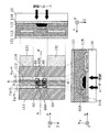
- FIG. 4 is a three-view diagram illustrating an example of the wiring structure of the drive circuit layer according to the embodiment.
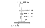
- FIG. 5 is a schematic configuration diagram of a laser irradiation system according to the embodiment.
- FIG. 6 is a flowchart for explaining a repair process of the display panel according to the embodiment.
- FIG. 7 is a trihedral view showing the wiring state of the drive circuit layer in the first laser irradiation step according to the embodiment.
- FIG. 8 is a three-plane view showing the wiring state of the drive circuit layer in the second laser irradiation step according to the embodiment.
- FIG. 9 is an external view of a thin flat TV having a built-in display panel
- the manufacturing method of the organic EL display panel according to the present embodiment includes (1) a laminating step of laminating a light emitting layer that constitutes an organic EL element that is a light emitting element and a driving circuit layer that constitutes a circuit element and wiring; 2) A laser irradiation step of irradiating a femtosecond laser to the wiring having a short-circuited portion from the side opposite to the light emitting layer side of the drive circuit layer.
- FIG. 1 is a structural cross-sectional view of an organic EL substrate.
- the organic EL substrate 1A shown in the figure is an organic functional device including an anode, a cathode, and an organic light emitting layer sandwiched between the two electrodes.
- one unit pixel formed by adjacently arranging a red pixel 200a, a green pixel 200b, and a blue pixel 200c (not shown) as sub-pixels in a matrix form.
- Each subpixel includes a driving circuit layer 11, a light emitting layer 12, a bank 13, a thin film sealing layer 141, a resin sealing layer 142, a color filter 143, and a transparent substrate 20 on the substrate 10.
- the substrate 10 and the transparent substrate 20 are substrates that protect the back surface and the light emitting surface of the organic EL substrate 1A, and are, for example, transparent alkali-free glass having a thickness of 0.5 mm.
- the drive circuit layer 11 is formed on the substrate 10 and includes a TFT (Thin Film Transistor) 111, wirings 112 and 113, a planarizing film 115, and an insulating film 116.
- TFT Thin Film Transistor
- the TFT 111 is a circuit element for driving emission of an organic EL element described later.
- the TFT 111 is, for example, a selection TFT that controls the timing of writing a signal voltage to each pixel, and a driving TFT that passes a current corresponding to the signal voltage to the organic EL element.
- the TFT 111 has an electrode wiring 114 that constitutes one of the source electrode and the drain electrode, and the electrode wiring that constitutes the other of the source electrode and the drain electrode is electrically connected to the anode 121.
- the wirings 112 and 113 are wirings for driving emission of organic EL elements to be described later.
- the light emitting layer 12 includes an anode 121, a hole injection layer 122, an organic light emitting layer 123, an electron transport layer 124, an electron injection layer 125, and a cathode 126, and constitutes an organic EL element that is a light emitting element. .
- the planarizing film 115 is a layer serving as a base of the light emitting layer 12 that is an upper layer of the drive circuit layer 11, and planarizes the uppermost surface of the drive circuit layer 11.
- the planarizing film 115 is made of, for example, an insulating organic material.
- the insulating film 116 is a layer for insulating and separating the substrate 10, the TFT 111, and the wirings 112 and 113.
- the anode 121 is an anode through which holes are supplied, that is, an electric current flows from an external circuit, and has a structure in which a reflective electrode made of, for example, Al or silver alloy APC is stacked on the planarizing film 115. Yes.
- the thickness of the reflective electrode is, for example, 10 to 40 nm.
- the hole injection layer 122 is a layer mainly composed of a hole injecting material.
- the hole injecting material is a material having a function of injecting holes injected from the anode 121 side into the organic light-emitting layer 123 stably or by assisting generation of holes.
- the organic light emitting layer 123 is a layer that emits light when a voltage is applied between the anode 121 and the cathode 126.
- ⁇ -NPD Bis [N- (1-naphthyl) -N-phenyl] benzidine is used as a lower layer.
- Alq3 tris- (8-hydroxyquinoline) aluminum is laminated as an upper layer.
- the electron transport layer 124 is a layer mainly composed of an electron transport material.
- the material having an electron transporting property has both the property of having an electron accepting property and easily becoming an anion, and the property of transmitting generated electrons by a charge transfer reaction between molecules, and charge transport from the cathode 126 to the organic light emitting layer 123. This material is suitable for
- the electron injection layer 125 is a layer mainly composed of an electron injecting material.
- the electron injecting material is a material having a function of injecting electrons injected from the cathode 126 into the organic light emitting layer 123 stably or by assisting generation of electrons.
- the cathode 126 is a cathode to which electrons are supplied, that is, a current flows out to an external circuit, and has a structure in which, for example, ITO is laminated as a transparent metal oxide.
- the thickness of the electrode is 10 to 40 nm as an example.
- the bank 13 is a wall for separating the organic light emitting layer 123 for each sub-pixel, and is made of, for example, a photosensitive resin.
- the thin film sealing layer 141 is made of, for example, silicon nitride and has a function of blocking the organic light emitting layer 123 and the cathode 126 from water vapor and oxygen. This is to prevent the organic light emitting layer 123 itself and the cathode 126 from being deteriorated (oxidized) by being exposed to water vapor or oxygen.
- the resin sealing layer 142 is an acrylic or epoxy resin, and joins the color filter 143 and the layer formed integrally from the planarization film 115 to the thin film sealing layer 141 formed on the substrate. .
- the color filter 143 is formed on the lower surface of the transparent substrate 20 as color filters 143a, 143b, and 143c (not shown) for adjusting the colors of red, green, and blue so as to cover each light emitting region separated by the bank 13. Has been.
- the color filter 143 has a black matrix 143d between the pixel regions.
- the color filter 143 may not be provided depending on the material configuration of the organic light emitting layer 123, and is not an essential component.
- the above-described configurations of the anode 121, the organic light emitting layer 123, and the cathode 126 are basic configurations of the organic EL element. With such a configuration, when an appropriate voltage is applied between the anode 121 and the cathode 126, Holes are injected into the organic light emitting layer 123 from the anode 121 side and electrons from the cathode 126 side, respectively. The energy generated by recombination of the injected holes and electrons in the organic light emitting layer 123 excites the light emitting material of the organic light emitting layer 123 to emit light.
- materials of the hole injection layer 122, the electron transport layer 124, and the electron injection layer 125 are not limited in the present embodiment, and a known organic material or inorganic material is used.
- each of the hole injection layer 122, the electron transport layer 124, and the electron injection layer 125 may not be disposed, and a hole transport layer may be disposed.
- FIG. 2 is a diagram for explaining repair handling when a display failure occurs due to a wiring short circuit.
- the left side of the figure shows the display state of the display panel when one data line 201 and one gate line 202 are short-circuited.
- the right side of the figure shows the display state of the display panel after repair. It is shown.
- a gate line 202 is arranged for each pixel row, and a data line 201 is arranged for each pixel column. Further, as shown on the left side of the figure, at the intersection A, the data line 201A and the gate line 202A are short-circuited. Thereby, a current path from the data line 201A to the gate line 202A is formed, and the signal voltage supplied to the data line 201A is not supplied to each red pixel 200a belonging to the pixel column in which the data line 201A is arranged.
- each red pixel 200a belonging to the pixel column does not emit light corresponding to the signal voltage and is always a dark spot pixel (in FIG. 2, the pixel is displayed in black indicates non-light emission), and the display panel On the upper side, a pixel row called a so-called red dark line is formed in which the red pixel 200a does not emit light.
- the short-circuit portion in the data line 201A is isolated. More specifically, the femtosecond laser is irradiated to the two regions sandwiching the intersection A in the data line 201A from the side opposite to the light emitting layer 12 with respect to the drive circuit layer 11 (from the substrate 10 side). Thereby, the data line 201A is disconnected (non-conducting) in the two regions. That is, the area of the data line 201A including the intersection A and sandwiched between the two areas is isolated from the other areas of the data line 201A.
- the area of the data line 201A including the intersection A may not be isolated in the above two areas, and the data line 201A may be disconnected in one of the two areas.
- the area of the data line 201A including the intersection A cannot be isolated, but the data line 201A is divided into two parts, that is, the area including the intersection A and the area not including the intersection A.
- the red pixel 200a connected to the area not including the intersection A can be converted into a normal pixel.
- FIG. 3 is a flowchart for explaining a method of manufacturing a display panel according to the embodiment.
- an organic EL substrate 1A is prepared (S10).
- the organic EL substrate 1A is a work-in-process in a manufacturing process of a display panel in which a plurality of pixels each having an organic EL element and circuit elements and wiring for driving the organic EL element to emit light are arranged. This step corresponds to a laminating step of laminating the light emitting layer 12 constituting the organic EL element and the driving circuit layer 11 constituting the circuit element and the wiring.
- step S10 the presence / absence of a short-circuit wiring is detected in the organic EL substrate 1A of the plurality of pixels formed in step S10 (S20).
- step S20 light emission to the drive circuit layer 11 is performed in two regions sandwiching the short-circuit portion in the wiring having the short-circuit portion short-circuited with the circuit element or other wiring.
- a femtosecond laser is irradiated from the side opposite to the layer 12 (S30).
- the process in step S30 is a characteristic process in the display panel manufacturing method according to the present embodiment.
- the driving circuit layer 11 including the TFT 111, the wirings 112 and 113, and the planarizing film 115 is formed on the substrate 10.
- the light emitting layer 12 is formed on the drive circuit layer 11.
- the anode 121 is formed by, for example, sputtering, depositing Al with a thickness of 30 nm on the planarizing film 115, and then performing a patterning process by photolithography and wet etching.
- the hole injection layer 122 is formed on the anode 121 by, for example, dissolving PEDOT in a solvent made of xylene and spin-coating this PEDOT solution.
- the organic light emitting layer 123 is formed by laminating ⁇ -NPD and Alq3 on the hole injection layer 122 by, for example, vacuum deposition.
- the electron transport layer 124 is formed on the organic light emitting layer 123.
- the electron injection layer 125 is formed on the electron transport layer 124, for example, by dissolving polyphenylene vinylene (PPV) in a solvent made of xylene or chloroform and spin-coating it.
- the cathode 126 is formed by depositing 35 nm of ITO (Indium Tin Oxide) on the electron injection layer 125 by a sputtering method.
- ITO Indium Tin Oxide
- silicon nitride is laminated on the cathode 126 by, for example, a plasma CVD (Chemical Vapor Deposition) method to form a thin film sealing layer 141.
- a plasma CVD Chemical Vapor Deposition
- the resin sealing layer 142 is applied to the surface of the thin film sealing layer 141. Thereafter, the color filter 143 and the transparent substrate 20 are disposed on the applied resin sealing layer 142. Specifically, for example, the transparent glass 18 on which the color filter 143 is formed is disposed on the applied resin sealing layer 142.
- the resin sealing layer 142 is cured by applying heat or energy rays while pressing the transparent substrate 20 downward from the upper surface side, and the transparent substrate 20 and the thin film sealing layer 141 are bonded.
- each formation process of the light emitting layer 12 is not limited by this Embodiment.
- step S20 first, a lighting inspection of the organic EL substrate 1A formed in step S10 is performed. Specifically, the light emission voltages emitted from the organic EL elements are simultaneously applied to all the pixels of the organic EL substrate 1A by the data line driving circuit and the scanning line driving circuit provided in the organic EL substrate 1A or in the lighting inspection device. This is applied to cause the organic EL element to emit light. All pixels are imaged by a CCD camera or the like during the light emission period of the organic EL element.
- the light emission luminance of each pixel is calculated from the captured image in the light emission period, and a pixel whose light emission luminance is a predetermined threshold value or less, that is, a so-called dark spot pixel is detected.
- the detected dark spot pixel is enlarged and observed. Specifically, for example, a dark spot pixel is observed using a camera microscope. At this time, a short-circuit portion of the wiring is specified in the area of the dark spot pixel that has been enlarged and observed.
- the detection of the short-circuit wiring is not limited to the method described above.
- a simple luminance meter or observation with the naked eye may be used without using a CCD camera.
- the femtosecond laser is irradiated to two regions sandwiching the short-circuited part by narrowing the beam diameter of the femtosecond laser so that the beam diameter of the femtosecond laser in the drive circuit layer 11 is substantially equal to the wiring width.
- the femtosecond laser is irradiated with the beam diameter narrowed so that the beam diameter is about the width of the wiring, so that the adjacent wiring with a narrow pitch is short-circuited without causing damage by the laser.
- the wiring can be deformed.
- the first laser irradiation is performed. It becomes possible to completely disconnect the corner portion of the short-circuit wiring that could not be completely cut in the process.
- the area of the data line including the short-circuited portion and sandwiched between the two areas can be isolated, and only the pixel connected to the isolated area is always a dark spot pixel, and other pixels can be relieved. It becomes possible. Therefore, the wiring having the short-circuited portion can be repaired with high accuracy and stability.
- FIG. 4 is a three-view diagram illustrating an example of the wiring structure of the drive circuit layer according to the embodiment.
- This figure shows a plan perspective view of the drive circuit layer 11 seen through from the image display side (Y-axis negative direction), and a sectional view when the plan perspective view is cut along AA ′ and BB ′.
- the wirings 112 and 113 and the electrode wiring 114 are arranged in parallel to each other.
- wirings 131 and 132 are arranged in parallel to each other in a direction orthogonal to the wirings 112 and 113 and the electrode wiring 114.
- the distance between the wirings 112 and 113 is, for example, 2 ⁇ m, and the distance between the wiring 112 and the electrode wiring 114 is, for example, 4 ⁇ m.
- the wiring 112 has a short circuit defect.
- a process of irradiating the wiring 112 with a femtosecond laser will be described.
- FIG. 5 is a schematic configuration diagram of a laser irradiation system according to the embodiment.
- the laser irradiation system shown in the figure includes a laser oscillator 101, a slit 102, a stage 103, an imaging lens 104, and an objective lens 105.
- the organic EL substrate 1 ⁇ / b> A is fixedly disposed on the stage 103.
- the laser oscillator 101 can oscillate, for example, a femtosecond pulse laser having a wavelength of 532 nm to 1600 nm and an output energy of 1 to 30 ⁇ J.
- a suitable pulse width of such a femtosecond pulse laser is 100 fsec (femtosecond) to 20 psec (picosecond).
- the amorphous (amorphous) state metal wiring can be easily deformed by irradiation with the femtosecond pulse laser.
- a laser focus is set on the wiring of the drive circuit layer 11, and the wiring is deformed.
- the outer periphery of the region irradiated with the laser beam on the wiring is also damaged, and adjacent wiring is damaged.
- a slit 102 having a slit width smaller than the beam condensing diameter and an imaging lens 104 as an imaging system are provided between the laser oscillator 101 and the objective lens 105.
- the objective lens 105 is, for example, 20 times larger, and in this embodiment, the slit width of the first slit used in the first laser irradiation step is 200 ⁇ m, and the slit of the second slit is used. The width is 100 ⁇ m.
- the beam diameter is 10 ⁇ m in the first laser irradiation process, and the beam diameter is 5 ⁇ m in the second laser irradiation process.
- stage 103 is movable in the height direction and the plane direction, and has a function of fixing an object to be repaired by laser.
- FIG. 6 is a flowchart for explaining a repair process of the display panel according to the embodiment.
- the femtosecond laser is irradiated from the back surface to the two regions sandwiching the short-circuited portion using the first slit so that the beam diameter on the wiring to be processed becomes substantially the wiring width (S31).
- the first laser irradiates the femtosecond laser to the two regions sandwiching the short-circuited part by narrowing the beam diameter of the femtosecond laser so that the beam diameter of the femtosecond laser in the drive circuit layer 11 becomes substantially the wiring width. It is an irradiation process.
- FIG. 7 is a three-sided view showing a wiring state of the drive circuit layer in the first laser irradiation step according to the embodiment.
- the drive circuit layer 11 is seen through from the image display side (Y-axis negative direction), a plan perspective view, and the plan perspective view is cut along AA ′ and BB ′. A cross-sectional view of the case is shown.
- step S31 the femtosecond laser 50 having a beam diameter substantially equal to the wiring width in the irradiation region 50A is irradiated to the irradiation region 50A from the side opposite to the light emitting layer 12 with respect to the drive circuit layer 11 (substrate 10 side).
- the wiring 112 in the irradiation region 50A is deformed, and the wiring 112 and the insulating film 116 below it are connected to the wiring. It is separated at the center.
- the femtosecond laser 50 is irradiated with the beam diameter reduced to be substantially the same as the wiring width, the wiring 112 can be processed without damaging the adjacent wiring 113 and electrode wiring 114. Yes. However, in this step, the wiring 112 and the insulating film 116 are in contact at both ends of the deformed wiring 112.
- the wiring 112 is deformed in the wiring extending direction, but the wiring 112 is continuous in the wiring end region. That is, in the state where Step S31 is performed, the wiring 112 is deformed in the irradiation region 50A, but is continuous in the wiring extending direction at the wiring end. According to this, the wiring 112 is not disconnected in the irradiation region 50A.
- a femtosecond laser is irradiated from the back surface to the corners of the two regions sandwiching the short-circuited portion using the second slit so that the beam diameter on the wiring to be processed is less than half of the wiring width (S32). ).
- step S32 the wiring extension of the two regions sandwiching the short-circuited part by reducing the beam diameter of the femtosecond laser so that the beam diameter of the femtosecond laser in the drive circuit layer 11 is smaller than the beam diameter in step S31.
- This is a second laser irradiation step of irradiating a femtosecond laser to a corner portion which is an end portion in the current direction and an end portion in the wiring width direction.
- FIG. 8 is a trihedral view showing the wiring state of the drive circuit layer in the second laser irradiation step according to the embodiment.
- the drive circuit layer 11 is seen through from the image display side (Y-axis negative direction), a plan perspective view, and the plan perspective view is cut along AA ′ and BB ′. A cross-sectional view of the case is shown.
- one irradiation region of the two regions sandwiching the short-circuit portion of the wiring 112 is shown.
- step S32 a femtosecond laser 60 having a beam diameter equal to or less than half the wiring width is applied to each of the four corner areas 60A that are the ends in the wiring extending direction and the wiring width direction of the irradiation region 50A. Irradiation from the side opposite to the light emitting layer 12 (substrate 10 side) with respect to the drive circuit layer 11
- the wiring 112 in the corner region 60A is deformed, and the wiring 112 and the insulating film 116 underneath are formed. It is separated at the wiring end.
- the wiring 112 is disconnected in the corner region 60A in the wiring extending direction.
- each of the four corner regions 60A is irradiated with the femtosecond laser 60.
- the two corner regions 60A adjacent in the wiring width direction may be irradiated with the femtosecond laser 60.
- the disconnection portion of the wiring 112 is not two but one.
- step S33 recovery lighting confirmation of the display panel subjected to steps S31 and S32 is performed (S33). If the pixel to be recovered emits light normally, the repair process is terminated. Note that if the light emission of the pixel to be recovered is insufficient, steps S31 to S33 may be executed again.
- the wiring 112 having a short-circuited portion that is short-circuited with another wiring or circuit element the wiring 112 can be disconnected in each of the two regions sandwiching the short-circuited portion.
- the short-circuit portion is isolated from the other region of the wiring 112.
- one embodiment of a method for manufacturing a display panel according to this embodiment is a display panel in which a plurality of pixels each including an organic EL element and circuit elements and wirings for driving the light-emitting element to emit light are arranged.
- the method includes the step of laminating the light emitting layer 12 constituting the organic EL element and the drive circuit layer 11 constituting the circuit element and the wiring, and a short-circuit portion short-circuited with the circuit element or other wiring.
- a predetermined region in the wiring 112 includes a laser irradiation step of irradiating a femtosecond laser from a side opposite to the light emitting layer 12 side of the drive circuit layer 11.
- the femtosecond laser is irradiated to the predetermined region by narrowing the beam diameter of the femtosecond laser so that the beam diameter of the femtosecond laser in the drive circuit layer 11 becomes substantially the wiring width.
- the beam diameter of the femtosecond laser is set so that the beam diameter of the femtosecond laser in the drive circuit layer 11 is smaller than the beam diameter in the first laser irradiation step.
- the femtosecond laser is irradiated with the beam diameter narrowed down so that the beam diameter is about the width of the wiring, so that the short circuit without causing damage to the adjacent wiring with a narrow pitch.
- the wiring can be deformed.
- the first laser irradiation is performed. It becomes possible to completely disconnect the corner portion of the short-circuit wiring that could not be completely cut in the process. Therefore, the wiring having the short-circuited portion can be repaired with high accuracy and stability.
- a femtosecond laser having a beam diameter of half or less of the wiring width may be irradiated to a plurality of corner portions in each of the two predetermined regions sandwiching the short-circuited portion.
- the femtosecond laser emitted from the light source is passed through the first slit arranged in the emission direction of the light source to irradiate the predetermined region with the femtosecond laser, and the second laser irradiation.
- the femtosecond laser emitted from the light source is passed through the second slit having a smaller slit diameter than the first slit, which is arranged in the emission direction from the light source, so that the predetermined region is irradiated with the femtosecond laser. May be.
- the beam diameter on the femtosecond laser wiring in the first laser irradiation step and the second laser irradiation step can be controlled with high accuracy.
- the configuration in which the lower electrode is an anode and the upper electrode is a cathode is shown, but the lower electrode may be a cathode and the upper electrode may be an anode.
- a substrate, a planarizing film, an anode, a hole injection layer, a light emitting layer, a partition wall, an electron transport layer, an electron injection layer, a cathode, a thin film sealing layer, a resin sealing layer, a color filter, and a transparent substrate, which are pixel structures Is not limited to the configuration shown in the above-described embodiment, and the material, configuration, and formation method may be changed.
- a hole transport layer may be provided between the hole injection layer and the light emitting layer.
- the present invention is suitable for manufacturing a thin flat TV system including a display panel manufactured by the manufacturing method according to the present embodiment as shown in FIG. 9, for example.
- the method for manufacturing a display panel according to the present invention is useful in technical fields such as flat-screen televisions and personal computer displays that require a large screen and high resolution.
Abstract
Description
本実施の形態に係る有機EL表示パネルの製造方法は、(1)発光素子である有機EL素子を構成する発光層と回路素子及び配線を構成する駆動回路層とを積層する積層工程と、(2)短絡箇所を有する配線に、駆動回路層の発光層側と反対の側から、フェムト秒レーザーを照射するレーザー照射工程とを含む。
図1は、有機EL基板の構造断面図である。同図に示した有機EL基板1Aは、陽極、陰極、および当該両極で挟まれた有機発光層を含む有機機能デバイスである。同図に記載された有機EL基板1Aは、サブ画素である赤色画素200a、緑色画素200b、及び、青色画素200c(図示せず)が隣接配置されて形成された1単位画素が、行列状に配置されている。各サブ画素は、基板10の上に、駆動回路層11と、発光層12と、バンク13と、薄膜封止層141と、樹脂封止層142と、カラーフィルタ143と、透明基板20とを備える。
ここで、上記構成の有機EL基板1Aにおいて、駆動回路層11の配線が短絡すると、例えば、駆動TFTが制御不能となり、各画素が適切に発光しないことが想定される。
以下、本実施の形態に係る表示パネルの製造方法について説明する。
まず、図2に示された有機EL基板1Aを準備する工程(S10)について説明する。
次に、有機EL基板1Aの短絡配線を検出する工程(S20)について説明する。図2に示すように、データ線201Aとゲート線202Aとが短絡すると、データ線201Aに接続された各画素は常時滅点画素となり、表示領域において滅線が発生する。
次に、本実施の形態に係る表示パネルの製造方法の要部である、短絡配線をレーザー照射によりリペアする工程(S30)について説明する。
以上のように、本実施の形態に係る表示パネルの製造方法の一態様は、有機EL素子と、当該発光素子を発光駆動するための回路素子及び配線とを有する画素が複数配置された表示パネルの製造方法であって、有機EL素子を構成する発光層12と、回路素子及び配線を構成する駆動回路層11とを積層する積層工程と、回路素子または他の配線と短絡した短絡箇所を有する配線112における所定領域に、駆動回路層11の発光層12側と反対の側から、フェムト秒レーザーを照射するレーザー照射工程とを含む。ここで、上記レーザー照射工程は、駆動回路層11におけるフェムト秒レーザーのビーム径が略配線幅となるように、フェムト秒レーザーのビーム径を絞って上記所定領域にフェムト秒レーザーを照射する第1レーザー照射工程と、第1レーザー照射工程の後、駆動回路層11におけるフェムト秒レーザーのビーム径が第1レーザー照射工程におけるビーム径よりも小さいビーム径となるように、フェムト秒レーザーのビーム径を絞って上記所定領域の配線延在方向の端部かつ配線幅方向の端部である角部にフェムト秒レーザーを照射することにより、上記所定領域において配線112を断線させる第2レーザー照射工程とを含む。
以上、上記実施の形態に基づいて表示パネルの製造方法を説明してきたが、本発明は、上述した実施の形態に限定されるものではない。実施の形態における任意の構成要素を組み合わせて実現される別の実施の形態や、実施の形態に対して本発明の主旨を逸脱しない範囲で当業者が思いつく各種変形を施して得られる変形例や、本実施の形態に係る表示パネルの製造方法により製造された表示パネルを内蔵した各種機器も本発明に含まれる。
10 基板
11 駆動回路層
12 発光層
13 バンク
20 透明基板
50、60 フェムト秒レーザー
50A 照射領域
60A 角部領域
101 レーザー発振器
102 スリット
103 ステージ
104 結像レンズ
105 対物レンズ
111 TFT
112、113、131、132 配線
114 電極配線
115 平坦化膜
116 絶縁膜
121 陽極
122 正孔注入層
123 有機発光層
124 電子輸送層
125 電子注入層
126 陰極
141 薄膜封止層
142 樹脂封止層
143、143a、143b、143c カラーフィルタ
143d ブラックマトリクス
200a、200aA 赤色画素
200b 緑色画素
200c 青色画素
201、201A データ線
202、202A ゲート線
Claims (3)
- 発光素子と、当該発光素子を発光駆動するための回路素子及び配線とを有する画素が複数配置された表示パネルの製造方法であって、
前記発光素子を構成する発光層と、前記回路素子及び前記配線を構成する駆動回路層とを積層する積層工程と、
前記回路素子または他の前記配線と短絡した短絡箇所を有する配線の所定領域に、前記駆動回路層の前記発光層側と反対の側から、フェムト秒レーザーを照射するレーザー照射工程とを含み、
前記レーザー照射工程は、
前記駆動回路層における前記フェムト秒レーザーのビーム径が略配線幅となるように、フェムト秒レーザーのビーム径を絞って前記所定領域に前記フェムト秒レーザーを照射する第1レーザー照射工程と、
前記第1レーザー照射工程の後、前記駆動回路層における前記フェムト秒レーザーのビーム径が前記第1レーザー照射工程における前記ビーム径よりも小さいビーム径となるように、フェムト秒レーザーのビーム径を絞って前記所定領域の配線延在方向の端部かつ配線幅方向の端部である角部にフェムト秒レーザーを照射することにより、前記所定領域において前記配線を断線させる第2レーザー照射工程とを含む
表示パネルの製造方法。 - 前記第2レーザー照射工程では、
前記短絡箇所を挟む2つの前記所定領域のそれぞれにおける複数の前記角部に対して、前記配線の幅の半分以下のビーム径を有する前記フェムト秒レーザーを照射する
請求項1に記載の表示パネルの製造方法。 - 前記第1レーザー照射工程では、
光源から出射したフェムト秒レーザーを、前記光源の出射方向に配置された第1スリットを通過させることにより、前記所定領域にフェムト秒レーザーを照射し、
前記第2レーザー照射工程では、
光源から出射したフェムト秒レーザーを、前記光源からの出射方向に配置された、前記第1スリットよりもスリット径の小さい第2スリットを通過させることにより、前記所定領域にフェムト秒レーザーを照射する
請求項1または2に記載の表示パネルの製造方法。
Priority Applications (2)
| Application Number | Priority Date | Filing Date | Title |
|---|---|---|---|
| JP2016527640A JP6405560B2 (ja) | 2014-06-12 | 2015-06-09 | 表示パネルの製造方法 |
| US15/317,331 US9882175B2 (en) | 2014-06-12 | 2015-06-09 | Method for manufacturing display panel |
Applications Claiming Priority (2)
| Application Number | Priority Date | Filing Date | Title |
|---|---|---|---|
| JP2014121705 | 2014-06-12 | ||
| JP2014-121705 | 2014-06-12 |
Publications (1)
| Publication Number | Publication Date |
|---|---|
| WO2015190092A1 true WO2015190092A1 (ja) | 2015-12-17 |
Family
ID=54833203
Family Applications (1)
| Application Number | Title | Priority Date | Filing Date |
|---|---|---|---|
| PCT/JP2015/002891 WO2015190092A1 (ja) | 2014-06-12 | 2015-06-09 | 表示パネルの製造方法 |
Country Status (3)
| Country | Link |
|---|---|
| US (1) | US9882175B2 (ja) |
| JP (1) | JP6405560B2 (ja) |
| WO (1) | WO2015190092A1 (ja) |
Cited By (2)
| Publication number | Priority date | Publication date | Assignee | Title |
|---|---|---|---|---|
| WO2019207798A1 (ja) * | 2018-04-27 | 2019-10-31 | シャープ株式会社 | 表示装置の製造方法および表示装置 |
| US11910696B2 (en) | 2020-11-09 | 2024-02-20 | Jdi Design And Development G.K. | Self-luminous display panel and self-luminous display panel manufacturing method |
Families Citing this family (5)
| Publication number | Priority date | Publication date | Assignee | Title |
|---|---|---|---|---|
| US10497892B2 (en) | 2016-03-03 | 2019-12-03 | Pioneer Corporation | Light-emitting device and light-emitting system |
| KR102603867B1 (ko) * | 2016-08-01 | 2023-11-21 | 삼성디스플레이 주식회사 | 유기 발광 표시 장치 및 유기 발광 표시 장치의 제조 방법 |
| CN107393939B (zh) * | 2017-08-30 | 2020-04-17 | 京东方科技集团股份有限公司 | 像素界定层及制造方法、显示面板及制造方法、显示装置 |
| CN110212111B (zh) * | 2019-05-30 | 2022-04-15 | 京东方科技集团股份有限公司 | 显示基板及制作方法、显示面板、显示装置 |
| KR20210048290A (ko) * | 2019-10-23 | 2021-05-03 | 삼성전자주식회사 | 디스플레이 장치 및 이의 제조 방법 |
Citations (4)
| Publication number | Priority date | Publication date | Assignee | Title |
|---|---|---|---|---|
| JP2002341304A (ja) * | 2001-05-15 | 2002-11-27 | Internatl Business Mach Corp <Ibm> | 液晶表示装置の修正方法、輝点欠陥部の修正方法、レーザ処理装置及び液晶表示装置 |
| JP2008122810A (ja) * | 2006-11-15 | 2008-05-29 | Sony Corp | Tft基板、表示装置、tft基板の製造方法、及び表示装置の製造方法 |
| WO2013038454A1 (ja) * | 2011-09-15 | 2013-03-21 | パナソニック株式会社 | 有機el素子の製造方法及び評価方法 |
| JP2013114749A (ja) * | 2011-11-24 | 2013-06-10 | Panasonic Corp | 有機el素子の製造方法 |
Family Cites Families (7)
| Publication number | Priority date | Publication date | Assignee | Title |
|---|---|---|---|---|
| JPH0614253B2 (ja) | 1984-02-07 | 1994-02-23 | セイコーエプソン株式会社 | 液晶表示装置 |
| KR20070038610A (ko) | 2005-10-06 | 2007-04-11 | 삼성전자주식회사 | 표시 장치의 수리 장치 및 수리 방법 |
| JP2008235178A (ja) | 2007-03-23 | 2008-10-02 | Sharp Corp | 有機elディスプレイの製造方法及び有機elディスプレイ |
| JP2009064607A (ja) | 2007-09-05 | 2009-03-26 | Sony Corp | 有機発光表示装置のリペア方法 |
| JP2009086499A (ja) * | 2007-10-02 | 2009-04-23 | Ntn Corp | 欠陥修正方法 |
| JP2012247547A (ja) | 2011-05-26 | 2012-12-13 | Sharp Corp | 配線の修正装置 |
| JP6277355B2 (ja) * | 2012-06-25 | 2018-02-14 | 株式会社Joled | 表示装置および表示装置の製造方法 |
-
2015
- 2015-06-09 US US15/317,331 patent/US9882175B2/en active Active
- 2015-06-09 JP JP2016527640A patent/JP6405560B2/ja active Active
- 2015-06-09 WO PCT/JP2015/002891 patent/WO2015190092A1/ja active Application Filing
Patent Citations (4)
| Publication number | Priority date | Publication date | Assignee | Title |
|---|---|---|---|---|
| JP2002341304A (ja) * | 2001-05-15 | 2002-11-27 | Internatl Business Mach Corp <Ibm> | 液晶表示装置の修正方法、輝点欠陥部の修正方法、レーザ処理装置及び液晶表示装置 |
| JP2008122810A (ja) * | 2006-11-15 | 2008-05-29 | Sony Corp | Tft基板、表示装置、tft基板の製造方法、及び表示装置の製造方法 |
| WO2013038454A1 (ja) * | 2011-09-15 | 2013-03-21 | パナソニック株式会社 | 有機el素子の製造方法及び評価方法 |
| JP2013114749A (ja) * | 2011-11-24 | 2013-06-10 | Panasonic Corp | 有機el素子の製造方法 |
Cited By (2)
| Publication number | Priority date | Publication date | Assignee | Title |
|---|---|---|---|---|
| WO2019207798A1 (ja) * | 2018-04-27 | 2019-10-31 | シャープ株式会社 | 表示装置の製造方法および表示装置 |
| US11910696B2 (en) | 2020-11-09 | 2024-02-20 | Jdi Design And Development G.K. | Self-luminous display panel and self-luminous display panel manufacturing method |
Also Published As
| Publication number | Publication date |
|---|---|
| US20170117506A1 (en) | 2017-04-27 |
| JPWO2015190092A1 (ja) | 2017-04-20 |
| US9882175B2 (en) | 2018-01-30 |
| JP6405560B2 (ja) | 2018-10-17 |
Similar Documents
| Publication | Publication Date | Title |
|---|---|---|
| JP6405560B2 (ja) | 表示パネルの製造方法 | |
| US9276231B2 (en) | Method for fabricating organic electroluminescence device and organic electroluminescence device | |
| JP5653944B2 (ja) | 有機el素子の製造方法及びレーザー焦点位置設定方法 | |
| US9040967B2 (en) | Method for manufacturing organic electroluminescence device and organic electroluminescence device | |
| US9425246B2 (en) | Organic light emitting display device and method of repairing the same | |
| JP6086333B2 (ja) | 有機エレクトロルミネッセンス表示装置の製造方法および有機エレクトロルミネッセンス表示装置 | |
| JP5963343B2 (ja) | 有機el素子の製造方法 | |
| JP6388291B2 (ja) | 有機エレクトロルミネッセンス素子の製造方法および有機エレクトロルミネッセンス素子 | |
| JP5958808B2 (ja) | 表示パネルの製造方法、その検査装置及び検査方法 | |
| JP5687339B2 (ja) | 有機el素子及び有機el素子の製造方法 | |
| US8093602B2 (en) | Stacked organic light-emitting device and imaging apparatus and image display apparatus having the same | |
| JP5963342B2 (ja) | 有機el素子の製造方法 | |
| JP6041087B2 (ja) | 表示パネルの製造方法、その検査装置及び検査方法 | |
| JP5938692B2 (ja) | 表示パネルの製造方法、その検査装置及び検査方法 | |
| WO2015111119A1 (ja) | 表示装置の製造方法および表示装置 | |
| JP6563311B2 (ja) | 表示パネルの製造方法および表示パネル | |
| JP6561290B2 (ja) | 表示パネルの製造方法および表示パネル | |
| JP2011124152A (ja) | 有機エレクトロルミネッセンス表示装置の製造方法および有機エレクトロルミネッセンス表示装置 |
Legal Events
| Date | Code | Title | Description |
|---|---|---|---|
| 121 | Ep: the epo has been informed by wipo that ep was designated in this application |
Ref document number: 15806232 Country of ref document: EP Kind code of ref document: A1 |
|
| WWE | Wipo information: entry into national phase |
Ref document number: 15317331 Country of ref document: US |
|
| ENP | Entry into the national phase |
Ref document number: 2016527640 Country of ref document: JP Kind code of ref document: A |
|
| NENP | Non-entry into the national phase |
Ref country code: DE |
|
| 122 | Ep: pct application non-entry in european phase |
Ref document number: 15806232 Country of ref document: EP Kind code of ref document: A1 |