WO2015178358A1 - パネルの製造方法 - Google Patents
パネルの製造方法 Download PDFInfo
- Publication number
- WO2015178358A1 WO2015178358A1 PCT/JP2015/064257 JP2015064257W WO2015178358A1 WO 2015178358 A1 WO2015178358 A1 WO 2015178358A1 JP 2015064257 W JP2015064257 W JP 2015064257W WO 2015178358 A1 WO2015178358 A1 WO 2015178358A1
- Authority
- WO
- WIPO (PCT)
- Prior art keywords
- glass
- mother substrate
- substrate
- base material
- liquid crystal
- Prior art date
- Legal status (The legal status is an assumption and is not a legal conclusion. Google has not performed a legal analysis and makes no representation as to the accuracy of the status listed.)
- Ceased
Links
Images




Classifications
-
- B—PERFORMING OPERATIONS; TRANSPORTING
- B23—MACHINE TOOLS; METAL-WORKING NOT OTHERWISE PROVIDED FOR
- B23K—SOLDERING OR UNSOLDERING; WELDING; CLADDING OR PLATING BY SOLDERING OR WELDING; CUTTING BY APPLYING HEAT LOCALLY, e.g. FLAME CUTTING; WORKING BY LASER BEAM
- B23K26/00—Working by laser beam, e.g. welding, cutting or boring
- B23K26/36—Removing material
- B23K26/362—Laser etching
- B23K26/364—Laser etching for making a groove or trench, e.g. for scribing a break initiation groove
-
- C—CHEMISTRY; METALLURGY
- C03—GLASS; MINERAL OR SLAG WOOL
- C03B—MANUFACTURE, SHAPING, OR SUPPLEMENTARY PROCESSES
- C03B33/00—Severing cooled glass
- C03B33/02—Cutting or splitting sheet glass or ribbons; Apparatus or machines therefor
- C03B33/023—Cutting or splitting sheet glass or ribbons; Apparatus or machines therefor the sheet or ribbon being in a horizontal position
- C03B33/027—Scoring tool holders; Driving mechanisms therefor
-
- C—CHEMISTRY; METALLURGY
- C03—GLASS; MINERAL OR SLAG WOOL
- C03B—MANUFACTURE, SHAPING, OR SUPPLEMENTARY PROCESSES
- C03B33/00—Severing cooled glass
- C03B33/07—Cutting armoured, multi-layered, coated or laminated, glass products
-
- C—CHEMISTRY; METALLURGY
- C03—GLASS; MINERAL OR SLAG WOOL
- C03B—MANUFACTURE, SHAPING, OR SUPPLEMENTARY PROCESSES
- C03B33/00—Severing cooled glass
- C03B33/09—Severing cooled glass by thermal shock
-
- G—PHYSICS
- G02—OPTICS
- G02F—OPTICAL DEVICES OR ARRANGEMENTS FOR THE CONTROL OF LIGHT BY MODIFICATION OF THE OPTICAL PROPERTIES OF THE MEDIA OF THE ELEMENTS INVOLVED THEREIN; NON-LINEAR OPTICS; FREQUENCY-CHANGING OF LIGHT; OPTICAL LOGIC ELEMENTS; OPTICAL ANALOGUE/DIGITAL CONVERTERS
- G02F1/00—Devices or arrangements for the control of the intensity, colour, phase, polarisation or direction of light arriving from an independent light source, e.g. switching, gating or modulating; Non-linear optics
- G02F1/01—Devices or arrangements for the control of the intensity, colour, phase, polarisation or direction of light arriving from an independent light source, e.g. switching, gating or modulating; Non-linear optics for the control of the intensity, phase, polarisation or colour
- G02F1/13—Devices or arrangements for the control of the intensity, colour, phase, polarisation or direction of light arriving from an independent light source, e.g. switching, gating or modulating; Non-linear optics for the control of the intensity, phase, polarisation or colour based on liquid crystals, e.g. single liquid crystal display cells
-
- G—PHYSICS
- G02—OPTICS
- G02F—OPTICAL DEVICES OR ARRANGEMENTS FOR THE CONTROL OF LIGHT BY MODIFICATION OF THE OPTICAL PROPERTIES OF THE MEDIA OF THE ELEMENTS INVOLVED THEREIN; NON-LINEAR OPTICS; FREQUENCY-CHANGING OF LIGHT; OPTICAL LOGIC ELEMENTS; OPTICAL ANALOGUE/DIGITAL CONVERTERS
- G02F1/00—Devices or arrangements for the control of the intensity, colour, phase, polarisation or direction of light arriving from an independent light source, e.g. switching, gating or modulating; Non-linear optics
- G02F1/01—Devices or arrangements for the control of the intensity, colour, phase, polarisation or direction of light arriving from an independent light source, e.g. switching, gating or modulating; Non-linear optics for the control of the intensity, phase, polarisation or colour
- G02F1/13—Devices or arrangements for the control of the intensity, colour, phase, polarisation or direction of light arriving from an independent light source, e.g. switching, gating or modulating; Non-linear optics for the control of the intensity, phase, polarisation or colour based on liquid crystals, e.g. single liquid crystal display cells
- G02F1/133—Constructional arrangements; Operation of liquid crystal cells; Circuit arrangements
- G02F1/1333—Constructional arrangements; Manufacturing methods
-
- G—PHYSICS
- G09—EDUCATION; CRYPTOGRAPHY; DISPLAY; ADVERTISING; SEALS
- G09F—DISPLAYING; ADVERTISING; SIGNS; LABELS OR NAME-PLATES; SEALS
- G09F9/00—Indicating arrangements for variable information in which the information is built-up on a support by selection or combination of individual elements
Definitions
- the present invention relates to a method for manufacturing a liquid crystal panel, an organic EL panel or the like.
- a liquid crystal panel includes two glass substrates facing each other, a color filter substrate on which BM, RGB, and photo spacers are patterned, and a TFT substrate on which thin film transistors and transparent electrodes are patterned. Yes. Both substrates are bonded to each other with a sealing material applied along their peripheral portions, and a liquid crystal material is sealed in a space surrounded by the sealing material between the two substrates.
- a plurality of LCD panels can be manufactured using the following method. Sometimes manufactured together.
- a first glass mother substrate formed by patterning BM, RGB, and photo spacers for a plurality of liquid crystal panels on a single glass plate, and a single glass plate.
- a second glass mother substrate formed by patterning thin film transistors and transparent electrodes for a plurality of surfaces is produced.
- the two base substrates are bonded together with a plurality of sealing materials, and a liquid crystal material is sealed in each of the spaces surrounded by the sealing materials, so that a liquid crystal panel base material including a plurality of liquid crystal panels is obtained. Make it.
- the liquid crystal panel base material is cut to obtain individual liquid crystal panels from the base material.
- Patent Document 1 discloses a method for cutting a liquid crystal panel base material when a liquid crystal panel is manufactured by the above-described technique.
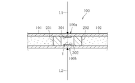
- the laser L1 A method of cutting the base material 100 by irradiating the laser L2 from the back side is disclosed.
- this method in each of the first glass mother substrate 100a existing on the front surface side of the liquid crystal panel base material 100 and the second glass mother substrate 100b existing on the rear surface side, on the back surface of the portion irradiated with the lasers L1 and L2, Films 301 and 302 having higher thermal conductivity than both mother substrates 100a and 100b are formed in advance.
- heat by laser irradiation is concentrated on the boundary Y through the films 301 and 302, and the base material 100 (both base substrates 100a and 100b) is cut.
- Patent Document 1 has the following problems to be solved. That is, in the method disclosed in the document, in order to cut the liquid crystal panel base material, in each of the first glass base substrate and the second glass base substrate, in all the portions that are the boundary of the adjacent liquid crystal panels, It is necessary to perform a film forming process in advance. Therefore, especially when there are a large number of liquid crystal panels to be cut out from the liquid crystal panel base material, the film forming process becomes complicated and the manufacturing efficiency is deteriorated, and an inherently unnecessary film is formed on the product. This also increases the manufacturing cost.
- the laser irradiated from the front surface side of the liquid crystal panel base material can cut only the first glass mother substrate, and the laser irradiated from the back surface side can only cut the second glass mother substrate. Can be cut. Therefore, in cutting the liquid crystal panel base material, it is essential to irradiate the laser from both the front surface side and the back surface side of the base material. And the glass cutting method using a laser tends to be expensive as compared with other glass cutting methods (for example, folding). For this reason, there is a concern about further increase in manufacturing cost due to the laser irradiation from both the front surface side and the back surface side.
- Such a problem is a problem that may occur not only when the liquid crystal panel base material is cut but also when other panel base materials such as a base material of an organic EL panel are cut.
- the present invention made in view of such circumstances is to enable cutting of a panel base material at a low cost and in a simple manner when cutting and manufacturing individual panels by cutting the panel base material. As an objective.
- the present invention which was created to solve the above problems, includes a first glass mother substrate provided with a first glass substrate in each region partitioned by a planned cutting line, and a first glass substrate facing each region.
- a second glass mother substrate provided with two glass substrates and a built-in member incorporated so as to be interposed between the first glass substrate and the second glass substrate in each region, the first in each region
- a panel base material including a glass substrate, a second glass substrate, and a panel including a built-in member as a component, and a panel manufacturing method including a cutting step of cutting the panel base material along a planned cutting line.
- an initial crack forming step for forming an initial crack at an end located on one end side of the planned cutting line in each of the first glass mother substrate and the second glass mother substrate, and to be cut into a panel base material Le along the line Heating by Heather irradiation, and, with the cooling by refrigerant to follow this to perform the one side of the panel base material, by progress together both initial crack, characterized in performing the cutting step.
- the irradiation source side mother substrate the mother substrate located on the laser irradiation source side (hereinafter referred to as the irradiation source side mother substrate) has a temperature gradient and thermal stress is generated. appear. Then, the initial crack propagates along the planned cutting line due to the thermal stress.
- the irradiation destination side mother substrate not only the irradiation source side mother substrate but also the mother substrate located on the laser irradiation destination side (hereinafter referred to as the irradiation destination side mother substrate) can propagate the initial crack along the planned cutting line. Is possible. It is assumed that such an effect is obtained for the following reason. That is, the built-in member is interposed between the irradiation source side mother board and the irradiation destination side mother board. Due to the interposition of this built-in member, the thermal stress generated in the irradiation-source side mother board propagates to the irradiation-destination-side mother board through the built-in member, and this propagated stress propagates the initial crack in the irradiation-destination-side mother board.
- both base substrates are cut by both initial cracks that propagate together, and the panel base material is cut.
- a panel base material first glass base substrate
- the second glass mother substrate the second glass mother substrate
- the initial crack forming step may be performed by rolling a scribe wheel.
- an end portion located on one end side of the planned cutting line in the first glass mother substrate and a first end side of the planned cutting line in the second glass mother substrate It is preferable that the end portion (hereinafter referred to as the second end portion) positioned is shifted and positioned in the direction in which the planned cutting line extends.
- both initial cracks can be obtained by rolling a single scribe wheel only once from one end side of the planned cutting line to the other end side or from the other end side to the one end side. Can be formed continuously.
- the length of deviation between the first end and the second end is 0.2 mm to 5 mm.
- the length that protrudes is 0.2 mm or more, scribe on the end portion that protrudes It is possible to ensure a sufficient length for the wheel to roll. Therefore, it is possible to suitably form an initial crack with respect to the end portion on the protruding side.
- the protruding length is 5 mm or less, it is possible to prevent as much as possible an increase in the number of parts that are inherently unnecessary in the panel base material (parts provided to form initial cracks). It is possible to avoid an unreasonable increase in manufacturing costs. From these facts, if the length of the first end portion and the second end portion is shifted to 0.2 mm to 5 mm, initial cracks can be suitably formed, and an unreasonable increase in manufacturing cost can be avoided. Is possible.
- the initial crack formation step by rolling the scribe wheel in a direction from the other end side to the one end side of the planned cutting line.
- the scribe wheel rolls from the inner side of the panel base material toward the outer peripheral end.
- the initial crack formation step may be performed by irradiating a pulse laser.
- the gap formed between the first glass mother substrate and the second glass mother substrate is extremely narrow. For this reason, when the first end portion and the second end portion are not shifted and positioned in the direction in which the planned cutting line extends (when the panel base material is viewed in a plan view, the first end portion and the second end portion Even if an attempt is made to form an initial crack by inserting a scribe wheel between the two mother substrates in a case where the portion overlaps the portion, it may be difficult to execute.
- the pulse laser it is possible to form an initial crack at a spot where the laser is condensed regardless of whether the first end and the second end are shifted from each other. . Thereby, both initial cracks can be reliably formed in a desired location.
- the laser irradiation conditions in the cutting step are the heating by laser irradiation on a glass plate having a thickness equal to or greater than the thickness of the first glass mother substrate and the second glass mother substrate, and this It is preferable that the initial crack formed at the end portion of the glass plate is advanced to be cut and cut by cooling with a refrigerant that follows.
- the panel base material can be suitably cut.
- the thickness of the first glass mother substrate and the second glass mother substrate is preferably 10 ⁇ m to 300 ⁇ m.
- the thickness of the first glass base substrate and the second glass base substrate is sufficiently thin, so that both glass base substrates can be prevented from being damaged when the panel base material is cut, and the panel base material is cut. It becomes easy to do.
- the width of the gap formed between the first glass mother substrate and the second glass mother substrate is preferably 0.1 ⁇ m to 20 ⁇ m.
- the present invention by cutting the panel base material, it is possible to cut the panel base material at low cost and easily when individual panels are cut out and manufactured.
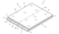
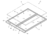
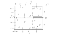
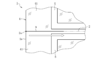
- FIG. 1 It is a perspective view which shows a liquid crystal panel base material. It is a perspective view which shows the state which removed the 1st glass base substrate virtually from the liquid crystal panel base material shown to FIG. It is a top view which shows the initial stage crack formation process in the manufacturing method of the panel which concerns on 1st embodiment of this invention. It is a top view which shows the initial stage crack formation process in the manufacturing method of the panel which concerns on 1st embodiment of this invention. It is a top view which shows the cutting process in the manufacturing method of the panel which concerns on 1st embodiment of this invention. It is a top view which shows the cutting process in the manufacturing method of the panel which concerns on 1st embodiment of this invention.
- FIG. 4a It is a top view which shows the state which removed the 1st glass mother board
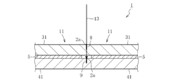
- the liquid crystal panel base material 1 includes a first glass base substrate provided with a first glass substrate 31 in each region (two regions in the present embodiment) defined by the planned cutting line 2. 3 and a second glass substrate 4 provided with a second glass substrate 41 facing the first glass substrate 31 in each region, and interposed between the first glass substrate 31 and the second glass substrate 41 in each region. And a sealing material 5 as a built-in member.
- the liquid crystal panel base material 1 includes the liquid crystal panel 11 that is a panel including the first glass substrate 31, the second glass substrate 41, and the sealing material 5 as components in each region. That is, the liquid crystal panel base material 1 includes two surfaces of liquid crystal panels 11.
- the first glass mother substrate 3 (first glass substrate 31) and the second glass mother substrate 4 (second glass substrate 41) are made of, for example, non-alkali glass.
- Each of the first glass mother substrate 3 and the second glass mother substrate 4 has a rectangular shape and a thickness of 10 ⁇ m to 300 ⁇ m.
- the width of the gap (cell gap) formed between the mother substrates 3 and 4 is 0.1 ⁇ m to 20 ⁇ m.
- Each first glass substrate 31 included in the first glass mother substrate 3 is a color filter substrate on which BM, RGB, and photo spacers (all of which are not shown) are patterned.
- each second glass substrate 41 included in the second glass mother substrate 4 is a TFT substrate on which a thin film transistor and a transparent electrode (both not shown) are patterned.
- the sealing material 5 is interposed between the first glass substrate 31 and the second glass substrate 41 to bond the substrates 31 and 41 together, and is formed along the peripheral edge of the substrates 31 and 41.
- a liquid crystal material (not shown) is sealed in the space 6 surrounded by the sealing material 5.
- a gap having a predetermined width is formed between the sealing materials 5 adjacent to each other with the planned cutting line 2 interposed therebetween.
- the sealing material 5 is made of, for example, an ultraviolet curable resin.
- An end 3a (hereinafter referred to as a first end 3a) located on one end 2a side of the planned cutting line 2 in the first glass mother substrate 3, and one end of the planned cutting line 2 in the second glass mother substrate 4
- the end 4a located on the 2a side (hereinafter referred to as the second end 4a) is shifted in the direction in which the planned cutting line 2 extends.
- the length Z in which the first end portion 3a and the second end portion 4a are displaced is set to 0.2 mm to 5 mm. Thereby, the second end 4a protrudes from the first end 3a.
- the thicknesses of the first glass mother substrate 3 and the second glass mother substrate 4 are more preferably 10 ⁇ m to 100 ⁇ m.
- the width of the gap formed between the mother substrates 3 and 4 is more preferably 0.1 ⁇ m to 10 ⁇ m, and most preferably 0.1 ⁇ m to 5 ⁇ m.
- the length Z in which the first end portion 3a and the second end portion 4a are displaced is more preferably 0.5 mm to 3 mm.
- the width of the gap formed between the adjacent sealing materials 5 is preferably 1 mm to 5 mm. If it does in this way, it will become easy to behave as the liquid crystal panel base material 1 is integrated.
- the method for manufacturing this panel is performed by the scribe wheel 7 on the first end 3a of the first glass mother substrate 3 and the second end 4a of the second glass mother substrate 4.
- An initial crack forming step (FIGS. 2a and 2b) for forming initial cracks 8 and 9, respectively, heating by laser irradiation along the planned cutting line 2 to the liquid crystal panel base material 1, and cooling by a refrigerant following this Is performed from the upper surface side of the liquid crystal panel base material 1, and both the initial cracks 8 and 9 are developed to cut the liquid crystal panel base material 1 (FIGS. 3, 4a, and 4b); Is included.
- the single scribe wheel 7 is rolled only once in the direction from the other end 2b side of the planned cutting line 2 to the one end 2a side. That is, the single scribe wheel 7 is rolled only once from the inner side of the liquid crystal panel base material 1 toward the outer peripheral end.
- the distance for rolling the scribe wheel 7 is preferably 1 mm to 10 mm.
- the scribe wheel 7 rolls on the first end portion 3a to form the initial crack 8, and then descends from the first end portion 3a to the second end portion 4a, and on the second end portion 4a. Roll to form an initial crack 9.
- both initial cracks 8 and 9 it is suitable when forming both the initial cracks 8 and 9 if the pressure which presses the scribe wheel 7 against the 1st end part 3a and the 2nd end part 4a is kept constant. Thereby, as shown in FIG. 2b, the formation of the initial crack 8 in the first end portion 3a and the formation of the initial crack 9 in the second end portion 4a are continuously performed. In the present embodiment, both initial cracks 8 and 9 are formed on the upper surface side of the first end portion 3a and the second end portion 4a.
- the liquid crystal panel base material 1 is heated by laser irradiation, and the cooling unit is cooled by jetting a coolant (for example, mist-like water). 12 are formed adjacent to each other.
- a coolant for example, mist-like water. 12 are formed adjacent to each other.
- laser irradiation and refrigerant injection are performed only from the upper surface side of the liquid crystal panel base material 1.
- the conditions of laser irradiation follow the heating by laser irradiation to a glass plate having a thickness equal to or more than the sum of the thickness of the first glass mother substrate 3 and the thickness of the second glass mother substrate 4, and follow this.
- the initial crack formed at the end of the glass plate is caused to be a condition for cutting.
- the laser irradiation condition may be a condition for cutting a glass plate having a thickness 1.1 to 2.1 times the sum of the thicknesses of both mother substrates 3 and 4 by laser cleaving.
- the laser irradiation condition may be a condition for cutting a glass plate having a thickness 1.4 to 2.0 times the sum of the thicknesses of both mother substrates 3 and 4 by laser cutting.
- the heating unit 10 and the cooling unit 12 are moved from the one end 2a side of the planned cutting line 2 toward the other end 2b side.
- the formation of the heating unit 10 and the cooling unit 12 is first performed only on the second end 4a protruding from the first end 3a.
- the temperature gradient generated by the heating unit 10 and the cooling unit 12 generates thermal stress, and the thermal stress propagates the initial crack 9 formed in the second end portion 4 a along the planned cutting line 2.
- the heating unit 10 and the cooling unit 12 are the first glass mothers that are constituent elements of the liquid crystal panel base material 1, as shown in FIG.
- the first glass mother substrate 3 positioned on the upper surface side (laser irradiation source side) of the liquid crystal panel base material 1 is formed.
- the initial crack 9 Advances along the planned cutting line 2, and the second glass mother substrate 4 is cut. That is, the initial crack 9 that has progressed through the second end 4a continues to progress.
- the sealing material 5 is interposed between the first glass mother substrate 3 and the second glass mother substrate 4.
- the thermal stress generated in the first glass mother substrate 3 is propagated to the second glass mother substrate 4 through the sealing material 5 due to the intervention of the sealing material 5, and the propagated stress is initially generated in the second glass mother substrate 4.
- the crack 9 is developed.
- the propagation of thermal stress is assumed to become more prominent as the first glass mother substrate 3 and the second glass mother substrate 4 are thinner. Thereby, both mother substrates 3 and 4 are cut, and the liquid crystal panel base material 1 is cut.
- the liquid crystal panel base material 1 is heated by laser irradiation along the planned cutting line 2 and cooled by a refrigerant that follows this, from the upper surface side, along with this,
- the liquid crystal panel base material 1 (the first glass base substrate 3 and the second glass base substrate 4) can be cut. Therefore, the liquid crystal panel base material 1 can be cut easily at low cost.
- the first end portion 3a and the second end portion 4a are shifted from each other in the direction in which the planned cutting line 2 extends, and the second end portion 4a protrudes from the first end portion 3a. ing. Therefore, in the initial crack formation step, the initial scribe wheel 7 is continuously rolled by rolling the single scribe wheel 7 only once from the other end 2b side of the planned cutting line 2 to the one end 2a side. Can be formed.
- the following effects can also be obtained by setting the length Z at which the first end portion 3a and the second end portion 4a are shifted to 0.2 mm to 5 mm. That is, it becomes possible to secure a sufficient length for the scribe wheel 7 to roll on the second end portion 4a, and an unnecessary portion (initial crack 9 is originally formed in the liquid crystal panel base material 1). It is possible to prevent as much as possible the number of parts to be formed to increase, and to avoid an unreasonable increase in manufacturing cost. These effects can be further enhanced by setting the length Z in which the first end portion 3a and the second end portion 4a are displaced within the range of 0.5 mm to 3 mm.
- the scribe wheel 7 is rolled in a direction from the other end 2b side of the planned cutting line 2 toward the one end 2a side.
- the scribe wheel 7 rolls from the inner side of the liquid crystal panel base material 1 toward the outer peripheral end. Therefore, when forming both the initial cracks 8 and 9, the rolling scribe wheel 7 cannot run up to the first end 3a or the second end 4a. For this reason, it is possible to avoid the first end portion 3a and the second end portion 4a from being unduly damaged by an impact at the time of riding.
- two glass substrates (OA-10G) manufactured by Nippon Electric Glass Co., Ltd. were prepared.
- a transparent glass or the like for two surfaces was formed on each of the two glass substrates to form a first glass mother substrate 3 and a second glass mother substrate 4, respectively.
- the thicknesses of both mother substrates 3 and 4 are 100 ⁇ m.
- the two mother boards 3 and 4 are bonded together with the sealing material 5 for two surfaces interposed therebetween, and a liquid crystal material is sealed in each of the spaces 6 surrounded by the sealing material 5 to include the liquid crystal panel 11 for two surfaces.
- a liquid crystal panel base material 1 was prepared. At this time, the width of the gap (cell gap) formed between the mother substrates 3 and 4 was set to 9 ⁇ m.
- Table 1 seven types of liquid crystal panel base materials 1 having different lengths Z from which the first end portion 3a and the second end portion 4a were shifted were produced.
- each liquid crystal panel base material 1 is heated by laser irradiation and cooled by spraying mist water that follows the liquid crystal panel base material 1, so that one end 2 a side of the planned cutting line 2 is changed from the other end 2 b side.
- the cutting of each liquid crystal panel base material 1 was attempted.
- the conditions for laser irradiation, the conditions for jetting mist water, and the conditions for forming both initial cracks 8 and 9 are common when cutting the liquid crystal panel base material 1, and are as follows.
- Laser type CO2 laser, laser wavelength: 10.6 ⁇ m, laser scanning speed: 25 mm / s, laser output: 15 W, mist water injection pressure: 0.06 MPa, mist water flow rate: 0.4 ml / min
- the diameter of the scribe wheel 7 is 3 mm, and the rolling speed of the scribe wheel 7 is 10 mm / s.
- the panel manufacturing method according to the second embodiment is different from the panel manufacturing method according to the first embodiment described above in the liquid crystal panel base material 1 to be cut in the first end 3a.
- both initial cracks 8 and 9 are formed by irradiation with a picosecond laser 13 as a pulse laser.
- the picosecond laser 13 is collected on the upper surfaces of the end portions 3a and 4a. It is illuminated (the top surface is the focal point of the picosecond laser 13).
- the formation of both initial cracks 8 and 9 may be performed by irradiating a femtosecond laser as a pulse laser instead of the picosecond laser 13.
- the wavelength of the pulse laser may be appropriately selected from various wavelengths according to the absorption rate of the first glass mother substrate 3 and the second glass mother substrate 4 and the pulse width of the pulse laser.
- the gap (cell gap) formed between the first glass mother substrate 3 and the second glass mother substrate 4 is extremely narrow. For this reason, when the first end portion 3a and the second end portion 4a are not shifted in the direction in which the planned cutting line 2 extends, the scribe wheel 7 is caused to enter between both the mother substrates 3 and 4. Even if the initial crack 9 is to be formed, the execution may be difficult. However, according to the picosecond laser 13, regardless of whether or not the first end portion 3a and the second end portion 4a are shifted from each other, the initial cracks are respectively generated at the locations where the picosecond laser 13 is condensed. 8, 9 can be formed. Thereby, both the initial cracks 8 and 9 can be reliably formed in a desired location.
- the panel manufacturing method according to the present invention is not limited to the mode described in each of the above embodiments.
- an individual liquid crystal panel is cut out by cutting a liquid crystal panel base material including liquid crystal panels for two surfaces.
- liquid crystal panels for three or more surfaces are included. Even when the liquid crystal panel base material is cut, the panel manufacturing method according to the present invention can be applied.
- both initial cracks may be formed by rolling a scribe wheel from one end side to the other end side. That is, both initial cracks may be formed by rolling the scribe wheel inward from the outer peripheral end of the liquid crystal panel base material.
- both initial cracks are continuously formed by rolling a single scribe wheel only once.
- individual initial cracks may be formed separately.
- both initial cracks are formed by irradiating a pulse laser such as a picosecond laser or a femtosecond laser, but this is not restrictive.
- both initial cracks may be formed by irradiating with a short wavelength laser such as a UV laser.
- a short wavelength laser such as a UV laser.
- it may replace with the scribe wheel in said 1st embodiment, and the pulse laser in 2nd embodiment, and may form both initial stage cracks using a sandpaper etc., for example.
- the initial crack in the initial crack forming step, is formed on the upper surface side of both the first end and the second end, but this is not restrictive. .
- an initial crack may be formed on either the upper surface side or the lower surface side.
- an initial crack may be formed on the upper surface side at the first end portion, and an initial crack may be formed on the lower surface side at the second end portion.
- the initial crack is formed on the first end portion and on the upper surface side and the lower surface side of the second end portion.
- the laser may be irradiated from the upper surface side of the liquid crystal panel base material, or may be irradiated from the lower surface side (the same applies when irradiating a short wavelength laser such as a UV laser).
- the scribe wheel is disposed in the thickness direction of the liquid crystal panel base material.
- the initial crack may be formed at the first end portion and the second end portion by rolling along.
- the liquid crystal panel base material is irradiated with laser only from the upper surface side and cooled by the refrigerant that follows this, but these are performed from the lower surface side. It is good also as an aspect performed only.
- the laser irradiation condition is a condition for cutting a glass plate having a thickness equal to or larger than the sum of the thicknesses of both mother substrates by laser cleaving, but this is not necessarily required.
- the individual liquid crystal panels are cut out by cutting the liquid crystal panel base material.
- the panel manufacturing method according to the present invention is, for example, an organic EL for a plurality of surfaces.
- the present invention can also be applied to a case where individual organic EL panels are cut out by cutting an organic EL panel base material including a panel.
Landscapes
- Physics & Mathematics (AREA)
- Chemical & Material Sciences (AREA)
- Engineering & Computer Science (AREA)
- Optics & Photonics (AREA)
- Nonlinear Science (AREA)
- Organic Chemistry (AREA)
- Materials Engineering (AREA)
- General Physics & Mathematics (AREA)
- Crystallography & Structural Chemistry (AREA)
- Mechanical Engineering (AREA)
- Mathematical Physics (AREA)
- Plasma & Fusion (AREA)
- Thermal Sciences (AREA)
- Theoretical Computer Science (AREA)
- Re-Forming, After-Treatment, Cutting And Transporting Of Glass Products (AREA)
- Liquid Crystal (AREA)
- Health & Medical Sciences (AREA)
- Toxicology (AREA)
Abstract
Description
はじめに、本発明の第一実施形態に係るパネルの製造方法において、切断の対象となる液晶パネル母材について説明する。

以下、本発明の第二実施形態に係るパネルの製造方法について説明する。なお、この第二実施形態の説明において、上記の第一実施形態で既に説明した要素と同一の要素については、第二実施形態を説明するための図面、及び説明文に同一の符号を付与することで重複する説明を省略している。また、第二実施形態では、上記の第一実施形態と相違する点についてのみ説明する。
11 液晶パネル
2 切断予定線
2a 切断予定線の一方端
3 第一ガラス母基板
3a 第一端部
31 第一ガラス基板
4 第二ガラス母基板
4a 第二端部
41 第二ガラス基板
5 シール材
7 スクライブホイール
8,9 初期クラック
13 ピコ秒レーザー
Claims (9)
- 切断予定線によって区画される各領域に第一ガラス基板を備えた第一ガラス母基板と、前記各領域に前記第一ガラス基板と対向する第二ガラス基板を備えた第二ガラス母基板と、前記各領域で前記第一ガラス基板と前記第二ガラス基板との間に介在するように組み込まれた組込部材とを有することで、前記各領域に前記第一ガラス基板、前記第二ガラス基板、及び前記組込部材を構成要素として含むパネルを備えたパネル母材について、該パネル母材を前記切断予定線に沿って切断する切断工程を含んだパネルの製造方法であって、
前記第一ガラス母基板、及び前記第二ガラス母基板の各々における前記切断予定線の一方端側に位置する端部に、それぞれ初期クラックを形成する初期クラック形成工程を含み、
前記パネル母材への前記切断予定線に沿ったレーザー照射による加熱、及び、これに追随する冷媒による冷却を該パネル母材の一方面側から行うのに伴って、両初期クラックを共に進展させることで、前記切断工程を実行することを特徴とするパネルの製造方法。 - 前記初期クラック形成工程を、スクライブホイールを転動させることで実行することを特徴とする請求項1に記載のパネルの製造方法。
- 前記第一ガラス母基板における前記切断予定線の一方端側に位置する端部と、前記第二ガラス母基板における前記切断予定線の一方端側に位置する端部とを、前記切断予定線が延びる方向にずらして位置させたことを特徴とする請求項2に記載のパネルの製造方法。
- 前記第一ガラス母基板における前記切断予定線の一方端側に位置する端部と、前記第二ガラス母基板における前記切断予定線の一方端側に位置する端部とがずれた長さを、0.2mm~5mmとしたことを特徴とする請求項3に記載のパネルの製造方法。
- 前記スクライブホイールを、前記切断予定線の他方端側から一方端側へと向かう方向に転動させることで、前記初期クラック形成工程を実行することを特徴とする請求項2~4のいずれかに記載のパネルの製造方法。
- 前記初期クラック形成工程を、パルスレーザーを照射することによって実行することを特徴とする請求項1に記載のパネルの製造方法。
- 前記切断工程における前記レーザー照射の条件を、
前記第一ガラス母基板の厚みと前記第二ガラス母基板の厚みとの和以上の厚みを有するガラス板に対し、レーザー照射による加熱、及び、これに追随する冷媒による冷却を行うことで、該ガラス板の端部に形成された初期クラックを進展させて切断する際の条件としたことを特徴とする請求項1~6のいずれかに記載のパネルの製造方法。 - 前記第一ガラス母基板、及び前記第二ガラス母基板の厚みを10μm~300μmとしたことを特徴とする請求項1~7のいずれかに記載のパネルの製造方法。
- 前記第一ガラス母基板と前記第二ガラス母基板との間に形成される隙間の幅を0.1μm~20μmとしたことを特徴とする請求項1~8のいずれかに記載のパネルの製造方法。
Priority Applications (3)
| Application Number | Priority Date | Filing Date | Title |
|---|---|---|---|
| KR1020167018415A KR102246031B1 (ko) | 2014-05-23 | 2015-05-19 | 패널의 제조 방법 |
| CN201580009294.7A CN106029591B (zh) | 2014-05-23 | 2015-05-19 | 面板的制造方法 |
| JP2016521098A JP6512221B2 (ja) | 2014-05-23 | 2015-05-19 | パネルの製造方法 |
Applications Claiming Priority (2)
| Application Number | Priority Date | Filing Date | Title |
|---|---|---|---|
| JP2014106947 | 2014-05-23 | ||
| JP2014-106947 | 2014-05-23 |
Publications (1)
| Publication Number | Publication Date |
|---|---|
| WO2015178358A1 true WO2015178358A1 (ja) | 2015-11-26 |
Family
ID=54554027
Family Applications (1)
| Application Number | Title | Priority Date | Filing Date |
|---|---|---|---|
| PCT/JP2015/064257 Ceased WO2015178358A1 (ja) | 2014-05-23 | 2015-05-19 | パネルの製造方法 |
Country Status (5)
| Country | Link |
|---|---|
| JP (1) | JP6512221B2 (ja) |
| KR (1) | KR102246031B1 (ja) |
| CN (1) | CN106029591B (ja) |
| TW (1) | TWI633963B (ja) |
| WO (1) | WO2015178358A1 (ja) |
Cited By (1)
| Publication number | Priority date | Publication date | Assignee | Title |
|---|---|---|---|---|
| CN114761365A (zh) * | 2020-02-06 | 2022-07-15 | 日本电气硝子株式会社 | 玻璃板的制造方法 |
Families Citing this family (2)
| Publication number | Priority date | Publication date | Assignee | Title |
|---|---|---|---|---|
| JP6578533B1 (ja) * | 2018-06-13 | 2019-09-25 | 株式会社Nsc | 液晶パネル製造方法 |
| KR102771296B1 (ko) * | 2021-04-08 | 2025-02-25 | 삼성디스플레이 주식회사 | 표시 패널용 모 기판의 절단 방법 |
Citations (3)
| Publication number | Priority date | Publication date | Assignee | Title |
|---|---|---|---|---|
| JP2007261885A (ja) * | 2006-03-29 | 2007-10-11 | Lemi Ltd | 重ねガラスの割断方法 |
| JP2010095414A (ja) * | 2008-10-17 | 2010-04-30 | Linkstar Japan Co Ltd | ディスプレイ用マザーガラス基板および脆性材料基板の切断方法、ディスプレイの製造方法 |
| JP2011116611A (ja) * | 2009-12-07 | 2011-06-16 | Nippon Electric Glass Co Ltd | 板状ガラスの切断方法及びその切断装置 |
Family Cites Families (5)
| Publication number | Priority date | Publication date | Assignee | Title |
|---|---|---|---|---|
| JP2002224870A (ja) | 2001-01-31 | 2002-08-13 | Seiko Epson Corp | レーザ切断方法、電気光学装置の製造方法、電気光学装置、および電子機器 |
| KR100626554B1 (ko) * | 2004-05-11 | 2006-09-21 | 주식회사 탑 엔지니어링 | 비금속재 절단장치 및 비금속재 절단시의 절단깊이 제어방법 |
| US8269138B2 (en) * | 2009-05-21 | 2012-09-18 | Corning Incorporated | Method for separating a sheet of brittle material |
| JP5904457B2 (ja) * | 2011-05-13 | 2016-04-13 | 日本電気硝子株式会社 | 積層体 |
| KR20150045957A (ko) * | 2012-08-21 | 2015-04-29 | 아사히 가라스 가부시키가이샤 | 복합 시트의 절단 방법, 유리 시트의 절단 방법, 복합 시트의 절단편 |
-
2015
- 2015-05-19 WO PCT/JP2015/064257 patent/WO2015178358A1/ja not_active Ceased
- 2015-05-19 KR KR1020167018415A patent/KR102246031B1/ko active Active
- 2015-05-19 JP JP2016521098A patent/JP6512221B2/ja active Active
- 2015-05-19 CN CN201580009294.7A patent/CN106029591B/zh active Active
- 2015-05-21 TW TW104116266A patent/TWI633963B/zh active
Patent Citations (3)
| Publication number | Priority date | Publication date | Assignee | Title |
|---|---|---|---|---|
| JP2007261885A (ja) * | 2006-03-29 | 2007-10-11 | Lemi Ltd | 重ねガラスの割断方法 |
| JP2010095414A (ja) * | 2008-10-17 | 2010-04-30 | Linkstar Japan Co Ltd | ディスプレイ用マザーガラス基板および脆性材料基板の切断方法、ディスプレイの製造方法 |
| JP2011116611A (ja) * | 2009-12-07 | 2011-06-16 | Nippon Electric Glass Co Ltd | 板状ガラスの切断方法及びその切断装置 |
Cited By (1)
| Publication number | Priority date | Publication date | Assignee | Title |
|---|---|---|---|---|
| CN114761365A (zh) * | 2020-02-06 | 2022-07-15 | 日本电气硝子株式会社 | 玻璃板的制造方法 |
Also Published As
| Publication number | Publication date |
|---|---|
| TW201607661A (zh) | 2016-03-01 |
| JPWO2015178358A1 (ja) | 2017-04-20 |
| TWI633963B (zh) | 2018-09-01 |
| CN106029591A (zh) | 2016-10-12 |
| JP6512221B2 (ja) | 2019-05-15 |
| KR20170010743A (ko) | 2017-02-01 |
| CN106029591B (zh) | 2019-08-23 |
| KR102246031B1 (ko) | 2021-04-29 |
Similar Documents
| Publication | Publication Date | Title |
|---|---|---|
| KR101528034B1 (ko) | 표시 장치의 제조 방법 | |
| US20170197868A1 (en) | Laser Processing of Electronic Device Structures | |
| TW201936309A (zh) | 複合材之斷開方法 | |
| JP2007260773A (ja) | 基板切断方法及びこれを用いた基板切断装置 | |
| CN101391860A (zh) | 利用超短脉冲激光束的基板切割装置及其切割方法 | |
| TWI637922B (zh) | 玻璃基板之倒角方法及雷射加工裝置 | |
| JP2008201629A (ja) | 電気光学装置の製造方法、基板の分断方法、及び、基板分断装置 | |
| CN104576698B (zh) | 一种有机发光二极管的阵列基板及其封装方法 | |
| EP2147899A1 (en) | Method for processing terminal in bonded substrate | |
| JP2009244598A (ja) | 母基板の分断方法および液晶表示装置の製造方法並びに液晶表示装置 | |
| TWI862553B (zh) | 複合材之分斷方法 | |
| CN105461207A (zh) | 分割方法及分割装置 | |
| JP2006199553A (ja) | 基板分断装置及び基板分断方法 | |
| WO2015178358A1 (ja) | パネルの製造方法 | |
| JP2009294461A (ja) | 液晶表示装置及びその製造方法 | |
| CN105044997B (zh) | 一种液晶显示面板及其制备方法、液晶显示装置 | |
| KR20140122312A (ko) | 액정표시장치 및 그 제조 방법 | |
| JP2009263159A (ja) | 貼り合わせガラス基板の加工方法 | |
| JP2009015131A (ja) | 表示装置の製造方法及び表示装置 | |
| KR102633196B1 (ko) | 스크라이빙 장치 및 스크라이빙 방법 | |
| JP2009190943A (ja) | 基板の分断装置、基板の分断方法、及びその方法を用いて製造された基板 | |
| JP2014048432A (ja) | セル基板の加工方法 | |
| JP2011183434A (ja) | レーザ加工方法 | |
| JP2007137699A (ja) | ガラス基板の切断方法 | |
| TWI433820B (zh) | 切割製程 |
Legal Events
| Date | Code | Title | Description |
|---|---|---|---|
| 121 | Ep: the epo has been informed by wipo that ep was designated in this application |
Ref document number: 15795445 Country of ref document: EP Kind code of ref document: A1 |
|
| ENP | Entry into the national phase |
Ref document number: 2016521098 Country of ref document: JP Kind code of ref document: A |
|
| ENP | Entry into the national phase |
Ref document number: 20167018415 Country of ref document: KR Kind code of ref document: A |
|
| NENP | Non-entry into the national phase |
Ref country code: DE |
|
| 122 | Ep: pct application non-entry in european phase |
Ref document number: 15795445 Country of ref document: EP Kind code of ref document: A1 |