WO2015178232A1 - 回路構成体および電気接続箱 - Google Patents
回路構成体および電気接続箱 Download PDFInfo
- Publication number
- WO2015178232A1 WO2015178232A1 PCT/JP2015/063433 JP2015063433W WO2015178232A1 WO 2015178232 A1 WO2015178232 A1 WO 2015178232A1 JP 2015063433 W JP2015063433 W JP 2015063433W WO 2015178232 A1 WO2015178232 A1 WO 2015178232A1
- Authority
- WO
- WIPO (PCT)
- Prior art keywords
- circuit board
- heat sink
- heat
- electronic component
- circuit structure
- Prior art date
- Legal status (The legal status is an assumption and is not a legal conclusion. Google has not performed a legal analysis and makes no representation as to the accuracy of the status listed.)
- Ceased
Links
Images





Classifications
-
- H—ELECTRICITY
- H05—ELECTRIC TECHNIQUES NOT OTHERWISE PROVIDED FOR
- H05K—PRINTED CIRCUITS; CASINGS OR CONSTRUCTIONAL DETAILS OF ELECTRIC APPARATUS; MANUFACTURE OF ASSEMBLAGES OF ELECTRICAL COMPONENTS
- H05K1/00—Printed circuits
- H05K1/02—Details
- H05K1/0201—Thermal arrangements, e.g. for cooling, heating or preventing overheating
- H05K1/0203—Cooling of mounted components
- H05K1/0204—Cooling of mounted components using means for thermal conduction connection in the thickness direction of the substrate
-
- B—PERFORMING OPERATIONS; TRANSPORTING
- B60—VEHICLES IN GENERAL
- B60R—VEHICLES, VEHICLE FITTINGS, OR VEHICLE PARTS, NOT OTHERWISE PROVIDED FOR
- B60R16/00—Electric or fluid circuits specially adapted for vehicles and not otherwise provided for; Arrangement of elements of electric or fluid circuits specially adapted for vehicles and not otherwise provided for
- B60R16/02—Electric or fluid circuits specially adapted for vehicles and not otherwise provided for; Arrangement of elements of electric or fluid circuits specially adapted for vehicles and not otherwise provided for electric constitutive elements
-
- H—ELECTRICITY
- H05—ELECTRIC TECHNIQUES NOT OTHERWISE PROVIDED FOR
- H05K—PRINTED CIRCUITS; CASINGS OR CONSTRUCTIONAL DETAILS OF ELECTRIC APPARATUS; MANUFACTURE OF ASSEMBLAGES OF ELECTRICAL COMPONENTS
- H05K1/00—Printed circuits
- H05K1/18—Printed circuits structurally associated with non-printed electric components
- H05K1/181—Printed circuits structurally associated with non-printed electric components associated with surface mounted components
-
- H—ELECTRICITY
- H05—ELECTRIC TECHNIQUES NOT OTHERWISE PROVIDED FOR
- H05K—PRINTED CIRCUITS; CASINGS OR CONSTRUCTIONAL DETAILS OF ELECTRIC APPARATUS; MANUFACTURE OF ASSEMBLAGES OF ELECTRICAL COMPONENTS
- H05K7/00—Constructional details common to different types of electric apparatus
- H05K7/20—Modifications to facilitate cooling, ventilating, or heating
- H05K7/20845—Modifications to facilitate cooling, ventilating, or heating for automotive electronic casings
- H05K7/20854—Heat transfer by conduction from internal heat source to heat radiating structure
-
- H—ELECTRICITY
- H02—GENERATION; CONVERSION OR DISTRIBUTION OF ELECTRIC POWER
- H02G—INSTALLATION OF ELECTRIC CABLES OR LINES, OR OF COMBINED OPTICAL AND ELECTRIC CABLES OR LINES
- H02G3/00—Installations of electric cables or lines or protective tubing therefor in or on buildings, equivalent structures or vehicles
- H02G3/02—Details
- H02G3/08—Distribution boxes; Connection or junction boxes
- H02G3/16—Distribution boxes; Connection or junction boxes structurally associated with support for line-connecting terminals within the box
-
- H—ELECTRICITY
- H05—ELECTRIC TECHNIQUES NOT OTHERWISE PROVIDED FOR
- H05K—PRINTED CIRCUITS; CASINGS OR CONSTRUCTIONAL DETAILS OF ELECTRIC APPARATUS; MANUFACTURE OF ASSEMBLAGES OF ELECTRICAL COMPONENTS
- H05K1/00—Printed circuits
- H05K1/02—Details
- H05K1/0201—Thermal arrangements, e.g. for cooling, heating or preventing overheating
- H05K1/0203—Cooling of mounted components
- H05K1/0209—External configuration of printed circuit board adapted for heat dissipation, e.g. lay-out of conductors, coatings
-
- H—ELECTRICITY
- H05—ELECTRIC TECHNIQUES NOT OTHERWISE PROVIDED FOR
- H05K—PRINTED CIRCUITS; CASINGS OR CONSTRUCTIONAL DETAILS OF ELECTRIC APPARATUS; MANUFACTURE OF ASSEMBLAGES OF ELECTRICAL COMPONENTS
- H05K2201/00—Indexing scheme relating to printed circuits covered by H05K1/00
- H05K2201/03—Conductive materials
- H05K2201/0332—Structure of the conductor
- H05K2201/0364—Conductor shape
- H05K2201/0382—Continuously deformed conductors
-
- H—ELECTRICITY
- H05—ELECTRIC TECHNIQUES NOT OTHERWISE PROVIDED FOR
- H05K—PRINTED CIRCUITS; CASINGS OR CONSTRUCTIONAL DETAILS OF ELECTRIC APPARATUS; MANUFACTURE OF ASSEMBLAGES OF ELECTRICAL COMPONENTS
- H05K2201/00—Indexing scheme relating to printed circuits covered by H05K1/00
- H05K2201/06—Thermal details
- H05K2201/066—Heatsink mounted on the surface of the printed circuit board [PCB]
-
- H—ELECTRICITY
- H05—ELECTRIC TECHNIQUES NOT OTHERWISE PROVIDED FOR
- H05K—PRINTED CIRCUITS; CASINGS OR CONSTRUCTIONAL DETAILS OF ELECTRIC APPARATUS; MANUFACTURE OF ASSEMBLAGES OF ELECTRICAL COMPONENTS
- H05K2201/00—Indexing scheme relating to printed circuits covered by H05K1/00
- H05K2201/10—Details of components or other objects attached to or integrated in a printed circuit board
- H05K2201/10227—Other objects, e.g. metallic pieces
- H05K2201/10272—Busbars, i.e. thick metal bars mounted on the printed circuit board [PCB] as high-current conductors
-
- H—ELECTRICITY
- H05—ELECTRIC TECHNIQUES NOT OTHERWISE PROVIDED FOR
- H05K—PRINTED CIRCUITS; CASINGS OR CONSTRUCTIONAL DETAILS OF ELECTRIC APPARATUS; MANUFACTURE OF ASSEMBLAGES OF ELECTRICAL COMPONENTS
- H05K2201/00—Indexing scheme relating to printed circuits covered by H05K1/00
- H05K2201/10—Details of components or other objects attached to or integrated in a printed circuit board
- H05K2201/10227—Other objects, e.g. metallic pieces
- H05K2201/10409—Screws
-
- H—ELECTRICITY
- H05—ELECTRIC TECHNIQUES NOT OTHERWISE PROVIDED FOR
- H05K—PRINTED CIRCUITS; CASINGS OR CONSTRUCTIONAL DETAILS OF ELECTRIC APPARATUS; MANUFACTURE OF ASSEMBLAGES OF ELECTRICAL COMPONENTS
- H05K3/00—Apparatus or processes for manufacturing printed circuits
- H05K3/0058—Laminating printed circuit boards onto other substrates, e.g. metallic substrates
- H05K3/0064—Laminating printed circuit boards onto other substrates, e.g. metallic substrates onto a polymeric substrate
Definitions
- the technology disclosed in this specification relates to a circuit structure and an electrical junction box.
- the electronic component mounted on the circuit board has a relatively large amount of heat generation, so if the heat generated from the electronic component is trapped in the case, the case becomes hot, and the electronic component housed in the case There was a possibility that the performance of this would deteriorate.
- circuit structure having a configuration in which a metal heat dissipating member is provided on a surface of a circuit board opposite to a surface on which electronic components are arranged has been proposed.
- the circuit board and the heat radiating member are first provided with an insulating layer on one surface side of the heat radiating member for insulation between the circuit board, and then an adhesive having high thermal conductivity is applied on the insulating layer. As a result, they are bonded to each other.
- thermosetting adhesive for example, there is a method of forming an insulating thin film by applying a thermosetting adhesive to the upper surface of the heat radiating member and heating it.
- thermosetting adhesive as the insulating layer
- a thermosetting adhesive as the insulating layer
- such an adhesive cures over time at room temperature, so printing, spraying, and other methods cannot be applied, and reliable insulation is achieved. It is difficult to form a uniform layer to obtain.
- the technology disclosed in the present specification has been completed based on the above-described circumstances, and an object thereof is to provide a circuit structure and an electrical junction box that are low in manufacturing cost and excellent in heat dissipation. It is.
- the technology disclosed in the present specification is a circuit configuration body including a heat sink, an insulating sheet stacked on the heat sink, and a circuit board stacked on the heat sink via the insulating sheet.
- the circuit board is fixed to the heat radiating plate by a fixing member, and a heat conductive member is disposed between the insulating sheet and the circuit board.
- the insulation between the heat sink and the circuit board is ensured by the insulating sheet. Further, the heat radiating plate and the circuit board are fixed to each other by a fixing member.
- a gap may be formed between the heat sink and the circuit board.
- the thermal conductivity may be lowered.
- the heat conductive member since the heat conductive member is arranged between the heat sink and the circuit board, the heat conductive member is in close contact with the heat sink and the circuit board. The heat generated in the circuit board is quickly transmitted to the heat radiating plate by the heat conductive member and radiated.
- the heat conductive member is placed in a region corresponding to the region on the circuit board where the electronic component is mounted. It is good also as a structure to provide. With such a configuration, a high heat dissipation effect can be obtained while reducing the amount of the heat conductive member to be used.
- the technology disclosed in this specification is an electrical junction box in which the above-described circuit structure is housed in a case.
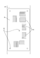
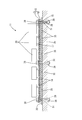
- top view of the heat sink of one embodiment Top view of insulation sheet Plan view of insulation sheet on heat sink A plan view of a state in which a heat conductive member is stacked on an insulating sheet Plan view of a circuit structure without electronic components AA exploded sectional view of FIG. AA sectional view of FIG. Side sectional view of a circuit structure according to another embodiment
- the electrical junction box 10 of this embodiment includes a circuit board 11 and a circuit structure 11 including a heat sink 25, and a synthetic resin case 40 that houses the circuit structure 11 (see FIG. 5).
- the upper side in FIG. 7 will be described as the front side or the upper side, and the lower side will be described as the back side or the lower side.
- the circuit structure 11 includes a circuit board 12, an electronic component 20 disposed on the surface of the circuit board 12 (upper surface in FIG. 1), and a back surface (lower surface in FIG. 1) of the circuit board 12. And a heat radiating plate 25 arranged.
- the circuit board 12 has a rectangular shape, and a conductive circuit (not shown) is formed on the surface of the insulating substrate 13 by printed wiring technology, and a plurality of bus bars 16 are arranged in a predetermined pattern on the back surface. Searched for.
- the plurality of bus bars 16 have a substantially rectangular shape, and are formed by pressing a metal plate material into a predetermined shape.
- board fixing holes 15 for penetrating bolts 38 an example of a fixing member for fixing the circuit board 12 to the heat sink 25 are provided.
- An electronic component 20 such as a relay is disposed on the surface of the circuit board 12. As shown in FIG. 5 and FIG. 7, a connection opening 14 for mounting the electronic component 20 on the bus bar 16 is formed at a position where the electronic component 20 is arranged on the insulating substrate 13. Each lead terminal of the component 20 is electrically connected to the land 17 of the conductive circuit or the surface of the bus bar 16 exposed through the connection opening 14 by a known method such as soldering.
- the heat sink 25 is disposed on the lower surface side (back surface side) of the bus bar 16 in the circuit board 12 (see FIG. 7).
- the heat radiating plate 25 is a plate-like member made of a metal material having excellent thermal conductivity such as aluminum or aluminum alloy, and has a function of radiating heat generated in the circuit board 12 and the electronic component 20.
- a heat sink fixing hole 26 is provided in a position corresponding to the substrate fixing hole 15 in the heat sink 25.
- an insulating sheet 30 for overlapping the heat radiating plate 25 and the circuit board 12 (bus bar 16) is overlaid.
- the insulating sheet 30 has a size slightly smaller than the upper surface of the heat sink 25 and has an adhesive property that can be fixed to the heat sink 25. Further, a sheet fixing hole 31 is provided through the insulating sheet 30 at a position corresponding to the heat sink fixing hole 26.
- a heat conductive member 35 is disposed between the insulating sheet 30 and a region of the bus bar 16 corresponding to the electronic component 20 (see FIGS. 5 and 7).
- the heat conductive member 35 is, for example, a viscous adhesive.
- a conductive circuit is formed on the front surface by a printed wiring technique, and solder is applied by screen printing to a predetermined position on the upper surface of the circuit board 12 in which bus bars 16 are arranged in a predetermined pattern on the back surface.
- solder is applied by screen printing to a predetermined position on the upper surface of the circuit board 12 in which bus bars 16 are arranged in a predetermined pattern on the back surface.
- the electronic component 20 is placed at a predetermined position, and reflow soldering is executed.
- the electronic component 20 is mounted on the surface side of the circuit board 12 (see FIG. 6).
- the insulating sheet 30 is overlaid on the upper surface of the heat radiating plate 25, and the whole is pressurized and adhered and fixed (see FIG. 3).
- the heat conductive member 35 is apply
- the heat conductive member 35 spreads so as to be crushed between the lower surface of the circuit board 12 (bus bar 16) and the upper surface of the insulating sheet 30, and is brought into close contact with both.
- circuit structure 11 is accommodated in the case 40 to form the electrical connection box 10.
- the insulating sheet 30 ensures insulation between the heat sink 25 and the circuit board 12 (bus bar 16). Therefore, it can be manufactured at a lower cost as compared with the conventional configuration in which the insulating layer is formed from a thermosetting resin which is expensive to manufacture.
- the heat radiating plate 25 and the circuit board 12 are configured to be fixed to each other by fastening bolts 38 and nuts 39. At this time, there may be a gap between the plate-like heat sink 25 and the circuit board 12, and in such a case, the thermal conductivity may be lowered.
- the heat conductive member 35 is disposed between the heat sink 25 and the circuit board 12, and the heat conductive member 35 is in close contact with both the heat sink 25 and the circuit board 12. Therefore, the heat generated in the circuit board 12 is quickly transmitted to the heat radiating plate 25 by the heat conductive member 35 and radiated.
- the heat conductive member 35 does not need adhesiveness, and the material can be easily selected. is there.
- the heat conductive member 35 is provided only in the region corresponding to the region where the electronic component 20 is mounted on the circuit board 12, the electronic component 20 is reduced while reducing the amount of the heat conductive member 35 to be used.
- the heat generated in can be quickly transmitted to the heat radiating plate 25 side, and a high heat radiating effect can be obtained.
- circuit structure 11 and the electrical junction box 10 that are low in manufacturing cost and excellent in heat dissipation.
- the heat conductive member 35 is provided only at a position corresponding to the electronic component 20.
- the heat conductive member 55 is provided on the entire upper surface of the heat radiating plate 25. It is good also as a structure.
- the thermally conductive member 35 is an adhesive having adhesiveness, but it is easily deformed so as to fill a gap between the circuit board 12 (bus bar 16) and the insulating sheet 30. As long as it adheres to both, another thing (for example, a gel-like sheet
- the position of the bolt 38 that fixes the circuit board 12 and the heat sink 25 is not limited to the above-described embodiment, and may be provided at other positions according to the rigidity of the circuit board 12. Further, the number of bolts 38 is not limited to the above embodiment.
Landscapes
- Engineering & Computer Science (AREA)
- Microelectronics & Electronic Packaging (AREA)
- Physics & Mathematics (AREA)
- Thermal Sciences (AREA)
- Mechanical Engineering (AREA)
- Cooling Or The Like Of Electrical Apparatus (AREA)
- Connection Or Junction Boxes (AREA)
- Architecture (AREA)
- Civil Engineering (AREA)
- Structural Engineering (AREA)
Abstract
放熱板25と、放熱板25に重ねられた絶縁シート30と、放熱板25に絶縁シート30を介して重ねられた回路基板12と、を有する回路構成体11であって、回路基板12はねじ止めにより放熱板25と固定されており、絶縁シート30と回路基板12との間に、熱伝導性部材35が配されている。
Description
本明細書によって開示される技術は、回路構成体および電気接続箱に関する。
従来より、車載電装品の通電や断電を実行する装置として、種々の電子部品が実装された回路基板を備える回路構成体をケースに収容してなるものが知られている。
このような装置において、回路基板に実装される電子部品は比較的発熱量が大きいため、電子部品から発生した熱がケース内にこもるとケース内が高温になり、ケース内に収容された電子部品の性能が低下する虞があった。
そこで従来から、回路基板や電子部品から発生した熱を放熱する様々な構造が提案されている。例えば、回路基板のうち電子部品が配された面の反対側の面に、金属製の放熱部材を設けた構成の回路構成体が提案されている。
回路基板と放熱部材とは、まず、放熱部材の一面側に回路基板との間の絶縁性を図るための絶縁層を設け、その後、絶縁層に重ねて熱伝導性の高い接着剤を塗布することにより、互いに接着される。
上述した絶縁層としては、例えば、放熱部材の上面に熱硬化性の接着剤を塗布して加熱することにより、絶縁性の薄膜を形成する方法がある。
しかし、絶縁層として熱硬化性の接着剤を塗布・硬化させる方法は、大掛かりな装置が必要となるため、製造コストがかかる。そこで、常温で硬化可能な接着剤を使用する方法が考えられるが、そのような接着剤は常温で経時的に硬化してしまうため印刷やスプレー等の工法を適用できず、確実な絶縁性を得るための均一な層を形成するのが困難である。
あるいは、両面に粘着性を有する絶縁シートを使用して、絶縁性と、放熱板および回路基板の接着との双方を実行させることも考えられるが、電子部品が実装された回路基板に対してむらなく一定の圧力をかけることは困難であり、放熱部材に対して均一な状態で回路基板を接着させることが難しい。
本明細書に開示される技術は上記のような事情に基づいて完成されたものであって、製造コストが低く、放熱性に優れる回路構成体および電気接続箱を提供することを目的とするものである。
本明細書に開示される技術は、放熱板と、前記放熱板に重ねられた絶縁シートと、前記放熱板に前記絶縁シートを介して重ねられた回路基板と、を有する回路構成体であって、前記回路基板は固定部材により前記放熱板と固定されており、前記絶縁シートと前記回路基板との間に、熱伝導性部材が配されていることを特徴とする。
このような構成によれば、まず、放熱板と回路基板とは、絶縁シートにより絶縁性が確保される。また、放熱板と回路基板とは、固定部材により、互いに固定される。
この時、放熱板と回路基板との間に隙間が生じる場合があり、そのような場合には、熱伝導性が低下する虞がある。しかし、本明細書に開示された技術によれば、放熱板と回路基板との間には熱伝導性部材が配される構成であるから、熱伝導性部材が放熱板および回路基板に密着し、回路基板で発生した熱はこの熱伝導性部材により速やかに放熱板に伝えられ、放熱される。
また、回路基板のうち放熱板が配される面と反対側の面に電子部品が実装される場合に、熱伝導性部材は、回路基板のうち電子部品が実装される領域に対応する領域に設ける構成としてもよい。このような構成とすると、使用する熱伝導性部材の量を減らしながらも、高い放熱効果を得ることができる。
また、本明細書に開示される技術は、上記回路構成体をケースに収容してなる電気接続箱である。
本明細書に開示される技術によれば、製造コストが低く、放熱性に優れる回路構成体および電気接続箱を得ることができる。
一実施形態を図1ないし図7によって説明する。
本実施形態の電気接続箱10は、回路基板12、および、放熱板25を含む回路構成体11と、回路構成体11を収容する合成樹脂製のケース40と、を備える(図5参照)。なお、以下の説明においては、図7における上側を表側又は上側とし、下側を裏側又は下側として説明する。
図7に示すように、回路構成体11は、回路基板12と、回路基板12の表面(図1における上面)に配された電子部品20と、回路基板12の裏面(図1における下面)に配された放熱板25とを備える。
図5に示すように、回路基板12は長方形状をなし、絶縁基板13の表面に、プリント配線技術により図示しない導電回路が形成されるとともに、裏面に、複数のバスバー16が所定のパターンで配索されてなる。複数のバスバー16は概ね矩形状をなしており、金属板材を所定形状にプレス加工してなる。回路基板12の四隅および中央部には、回路基板12を放熱板25に固定するボルト38(固定部材の一例)を貫通するための基板用固定孔15が設けられている。
回路基板12の表面には、リレー等の電子部品20が配されている。図5および図7に示すように、絶縁基板13のうち電子部品20が配される位置には、電子部品20をバスバー16上に実装するための接続用開口部14が形成されており、電子部品20の各リード端子は、例えばハンダ付け等公知の手法により、導電回路のランド17上、または、接続用開口部14を通して露出されたバスバー16の表面に、電気的に接続されている。
回路基板12のうちバスバー16の下面側(裏面側)には、放熱板25が配置されている(図7参照)。放熱板25は、例えばアルミニウムやアルミニウム合金等の熱伝導性に優れる金属材料からなる板状部材であり、回路基板12および電子部品20において発生した熱を放熱する機能を有する。放熱板25のうち、上述した基板用固定孔15に対応する位置には、放熱板用固定孔26が設けられている。
放熱板25の上面には、放熱板25と回路基板12(バスバー16)との間の絶縁性を図るための絶縁シート30が重ねられている。絶縁シート30は、放熱板25の上面より一回り小さいサイズとされており、放熱板25に対して固定可能な接着性を有している。また絶縁シート30のうち、放熱板用固定孔26に対応する位置には、シート用固定孔31が貫通して設けられている。
さらに、絶縁シート30と、バスバー16のうち電子部品20と対応する領域との間には、熱伝導性部材35が配されている(図5および図7参照)。本実施形態において、熱伝導性部材35は、例えば粘性を有する接着剤である。
続いて、本実施形態に係る電気接続箱10の製造工程の一例を説明する。まず、表面に導電回路がプリント配線技術により形成されるとともに、裏面にバスバー16が所定のパターンで配策された回路基板12の上面の所定位置に、スクリーン印刷によりはんだを塗布する。その後、所定の位置に電子部品20を載置し、リフローはんだ付けを実行する。これにより、回路基板12の表面側に電子部品20が実装された状態とされる(図6参照)。
次に、放熱板25の上面に絶縁シート30を重ね合わせ、全体を加圧して密着・固定させる(図3参照)。そして、絶縁シート30のうち、回路基板12が重ねられた場合に電子部品20と対応する領域に熱伝導性部材35を塗布し(図4参照)、その後、電子部品20を実装した回路基板12を上方から重ね合わせる。この時、熱伝導性部材35は回路基板12(バスバー16)の下面と絶縁シート30の上面との間に押し潰されるように広がり、両者に密着した状態とされる。
その後、連通状態とされた基板用固定孔15、シート用固定孔31、および、放熱板用固定孔26にボルト38を貫通させて、ナット39(固定部材の一例)を締結する。これにより、回路基板12および放熱板25が互いに固定された回路構成体11が完成する(図5ないし図7参照)。なお、図5においては、熱伝導性部材35と、接続用開口部14およびランド17との位置関係を明確にするために、搭載されている電子部品20を省略している。
最後に、回路構成体11をケース40内に収容し、電気接続箱10とする。
続いて、本実施形態に係る回路構成体11および電気接続箱10の作用、効果について説明する。本実施形態の回路構成体11および電気接続箱10によれば、放熱板25と回路基板12(バスバー16)とは、絶縁シート30により絶縁性が確保される。従って、製造コストがかかる熱硬化性樹脂により絶縁層を形成する従来の構成と比較して、安価に製造することができる。
また、放熱板25と回路基板12とは、ボルト38およびナット39の締結により互いに固定される構成とされている。この時、ともに板状の放熱板25と回路基板12との間に隙間が生じる場合があり、そのような場合には、熱伝導性が低下する虞がある。しかし本実施形態によれば、放熱板25と回路基板12との間には熱伝導性部材35が配されており、この熱伝導性部材35が放熱板25および回路基板12の双方に密着しているから、回路基板12で発生した熱はこの熱伝導性部材35により速やかに放熱板25に伝えられ、放熱される。
しかも、上述したように、放熱板25と回路基板12とは、ボルト38およびナット39の締結により互いに固定されているから、熱伝導性部材35に接着性は必要なく、材料の選択が容易である。
さらに、熱伝導性部材35を回路基板12のうち電子部品20が実装される領域に対応する領域のみに設ける構成としたから、使用する熱伝導性部材35の量を減らしながらも、電子部品20において発せられた熱を速やかに放熱板25側に伝えることができ、高い放熱効果を得ることができる。
すなわち、製造コストが低く、放熱性に優れる回路構成体11および電気接続箱10を得ることができる。
<他の実施形態>
本明細書によって開示される技術は上記記述及び図面によって説明した実施形態に限定されるものではなく、例えば次のような種々の態様も含まれる。
本明細書によって開示される技術は上記記述及び図面によって説明した実施形態に限定されるものではなく、例えば次のような種々の態様も含まれる。
(1)上記実施形態では、熱伝導性部材35を電子部品20に対応する位置だけに設ける構成としたが、図8に示すように、熱伝導性部材55を放熱板25の上面全体に設ける構成としてもよい。
(2)上記実施形態では、熱伝導性部材35は、粘着性を有する接着剤としたが、容易に変形して回路基板12(バスバー16)と絶縁シート30との間の隙間を埋めるように両者に密着するものであれば他のもの(例えばゲル状のシート)でもよく、上記実施形態に限るものではない。
(3)回路基板12と放熱板25とを固定するボルト38の位置は、上記実施形態に限らず、回路基板12の剛性に合わせて他の位置に設けてもよい。また、ボルト38の数も上記実施形態に限るものではない。
10:電気接続箱
11:回路構成体
12:回路基板
14:接続用開口部
16:バスバー
20:電子部品
25:放熱板
30:絶縁シート
35:熱伝導性部材
38:ボルト(固定部材)
39:ナット(固定部材)
40:ケース
11:回路構成体
12:回路基板
14:接続用開口部
16:バスバー
20:電子部品
25:放熱板
30:絶縁シート
35:熱伝導性部材
38:ボルト(固定部材)
39:ナット(固定部材)
40:ケース
Claims (4)
- 放熱板と、
前記放熱板に重ねられた絶縁シートと、
前記放熱板に前記絶縁シートを介して重ねられた回路基板と、を有する回路構成体であって、
前記回路基板は固定部材により前記放熱板と固定されており、
前記絶縁シートと前記回路基板との間に、熱伝導性部材が配されている回路構成体。 - 前記回路基板のうち前記放熱板が配される面と反対側の面に電子部品が実装されており、
前記熱伝導性部材は、前記回路基板のうち前記電子部品が実装される領域に対応する領域に設けられている請求項1に記載の回路構成体。 - 前記回路基板のうち前記電子部品が実装される領域は、前記電子部品のリード端子のうち、一のリード端子から他のリード端子の間に設けられている請求項2に記載の回路構成体。
- 請求項1ないし請求項3のいずれか一項に記載の回路構成体をケースに収容してなる電気接続箱。
Priority Applications (3)
| Application Number | Priority Date | Filing Date | Title |
|---|---|---|---|
| US15/308,859 US10117322B2 (en) | 2014-05-23 | 2015-05-11 | Circuit assembly and electric junction box |
| CN201580024044.0A CN106463930A (zh) | 2014-05-23 | 2015-05-11 | 电路结构体及电连接箱 |
| DE112015002430.1T DE112015002430T5 (de) | 2014-05-23 | 2015-05-11 | Schaltungsbaugruppe und elektrischer Verteiler |
Applications Claiming Priority (2)
| Application Number | Priority Date | Filing Date | Title |
|---|---|---|---|
| JP2014-106803 | 2014-05-23 | ||
| JP2014106803A JP2015223044A (ja) | 2014-05-23 | 2014-05-23 | 回路構成体および電気接続箱 |
Publications (1)
| Publication Number | Publication Date |
|---|---|
| WO2015178232A1 true WO2015178232A1 (ja) | 2015-11-26 |
Family
ID=54553905
Family Applications (1)
| Application Number | Title | Priority Date | Filing Date |
|---|---|---|---|
| PCT/JP2015/063433 Ceased WO2015178232A1 (ja) | 2014-05-23 | 2015-05-11 | 回路構成体および電気接続箱 |
Country Status (5)
| Country | Link |
|---|---|
| US (1) | US10117322B2 (ja) |
| JP (1) | JP2015223044A (ja) |
| CN (1) | CN106463930A (ja) |
| DE (1) | DE112015002430T5 (ja) |
| WO (1) | WO2015178232A1 (ja) |
Families Citing this family (17)
| Publication number | Priority date | Publication date | Assignee | Title |
|---|---|---|---|---|
| JP2016119798A (ja) * | 2014-12-22 | 2016-06-30 | 株式会社オートネットワーク技術研究所 | 回路構成体及び電気接続箱 |
| JP6477373B2 (ja) * | 2015-09-11 | 2019-03-06 | 株式会社オートネットワーク技術研究所 | 回路構成体および電気接続箱 |
| KR102495931B1 (ko) * | 2015-12-15 | 2023-02-02 | 엘지디스플레이 주식회사 | 인쇄 회로 기판 및 이를 포함하는 표시 장치 |
| JP6443632B2 (ja) * | 2015-12-16 | 2018-12-26 | 株式会社オートネットワーク技術研究所 | 回路構成体、及び電気接続箱 |
| JP2017117902A (ja) * | 2015-12-24 | 2017-06-29 | 株式会社オートネットワーク技術研究所 | 回路構成体 |
| JP2017152441A (ja) * | 2016-02-22 | 2017-08-31 | 株式会社オートネットワーク技術研究所 | 回路構成体 |
| WO2018105465A1 (ja) | 2016-12-09 | 2018-06-14 | 三菱電機株式会社 | 電子回路基板、電力変換装置 |
| JP2018164324A (ja) * | 2017-03-24 | 2018-10-18 | 株式会社オートネットワーク技術研究所 | 電気接続箱 |
| CN110914936A (zh) * | 2017-05-24 | 2020-03-24 | 株式会社自动网络技术研究所 | 电路结构体 |
| DE102018207943A1 (de) * | 2018-05-22 | 2019-11-28 | Zf Friedrichshafen Ag | Elektronikmodul zur Anordnung an einem Getriebebauteil und Verfahren zur Anordnung eines Elektronikmoduls an einem Getriebebauteil |
| JP2020088086A (ja) * | 2018-11-21 | 2020-06-04 | 株式会社オートネットワーク技術研究所 | 回路構成体 |
| JP7052689B2 (ja) | 2018-11-21 | 2022-04-12 | 株式会社オートネットワーク技術研究所 | 回路構成体 |
| JP2021005652A (ja) * | 2019-06-26 | 2021-01-14 | 株式会社オートネットワーク技術研究所 | 回路構成体 |
| US11670929B2 (en) * | 2021-06-02 | 2023-06-06 | Schaeffler Technologies AG & Co. KG | Heat dissipation and sealing configuration for junction assembly |
| JP7596947B2 (ja) * | 2021-06-16 | 2024-12-10 | 住友電装株式会社 | 回路構造体 |
| US11955871B2 (en) * | 2021-09-28 | 2024-04-09 | Schaeffler Technologies AG & Co. KG | Emotor connection arrangement with phase bar cooling and compliant internal support in the junction box |
| DE102025111437A1 (de) * | 2024-04-24 | 2025-10-30 | Sew-Eurodrive Gmbh & Co Kg | Elektrogerät mit einem Gehäuseteil |
Citations (3)
| Publication number | Priority date | Publication date | Assignee | Title |
|---|---|---|---|---|
| JP2003179316A (ja) * | 2001-12-13 | 2003-06-27 | Fuji Kiko Denshi Kk | 放熱性に優れたプリント配線板の構造 |
| JP2005151624A (ja) * | 2003-11-11 | 2005-06-09 | Sumitomo Wiring Syst Ltd | 回路構成体の製造方法 |
| JP2010232318A (ja) * | 2009-03-26 | 2010-10-14 | Toyota Industries Corp | 半導体装置および熱伝シート |
Family Cites Families (18)
| Publication number | Priority date | Publication date | Assignee | Title |
|---|---|---|---|---|
| US5708566A (en) * | 1996-10-31 | 1998-01-13 | Motorola, Inc. | Solder bonded electronic module |
| CN1146988C (zh) * | 1997-12-08 | 2004-04-21 | 东芝株式会社 | 半导体功率器件的封装及其组装方法 |
| JPH11330709A (ja) * | 1998-05-14 | 1999-11-30 | Ishikawajima Harima Heavy Ind Co Ltd | ヒートシンク付メタルクラッド基板 |
| US6156980A (en) * | 1998-06-04 | 2000-12-05 | Delco Electronics Corp. | Flip chip on circuit board with enhanced heat dissipation and method therefor |
| JP2001135758A (ja) * | 1999-11-04 | 2001-05-18 | Toyota Autom Loom Works Ltd | パワーモジュールの放熱構造 |
| US6549409B1 (en) * | 2000-08-21 | 2003-04-15 | Vlt Corporation | Power converter assembly |
| JP3927017B2 (ja) | 2001-11-26 | 2007-06-06 | 株式会社オートネットワーク技術研究所 | 回路構成体及びその製造方法 |
| US7167377B2 (en) | 2001-11-26 | 2007-01-23 | Sumitoo Wiring Systems, Ltd. | Circuit-constituting unit and method of producing the same |
| US6724631B2 (en) * | 2002-04-22 | 2004-04-20 | Delta Electronics Inc. | Power converter package with enhanced thermal management |
| KR100696832B1 (ko) * | 2005-08-30 | 2007-03-19 | 삼성에스디아이 주식회사 | 플라즈마 디스플레이 모듈 |
| JP4278680B2 (ja) * | 2006-12-27 | 2009-06-17 | 三菱電機株式会社 | 電子制御装置 |
| JP4385058B2 (ja) * | 2007-05-07 | 2009-12-16 | 三菱電機株式会社 | 電子制御装置 |
| JP2010245174A (ja) * | 2009-04-02 | 2010-10-28 | Denso Corp | 電子制御ユニット及びその製造方法 |
| US8520389B2 (en) * | 2009-12-02 | 2013-08-27 | Hamilton Sundstrand Corporation | Power semiconductor module for wide temperature applications |
| JP5546889B2 (ja) * | 2010-02-09 | 2014-07-09 | 日本電産エレシス株式会社 | 電子部品ユニット及びその製造方法 |
| US8737073B2 (en) * | 2011-02-09 | 2014-05-27 | Tsmc Solid State Lighting Ltd. | Systems and methods providing thermal spreading for an LED module |
| KR101986694B1 (ko) * | 2012-04-11 | 2019-06-07 | 가부시키가이샤 리키드 디자인 시스템즈 | 조명 장치 및 액정표시장치 |
| US9257310B2 (en) * | 2012-10-19 | 2016-02-09 | Haesung Ds Co., Ltd. | Method of manufacturing circuit board and chip package and circuit board manufactured by using the method |
-
2014
- 2014-05-23 JP JP2014106803A patent/JP2015223044A/ja active Pending
-
2015
- 2015-05-11 DE DE112015002430.1T patent/DE112015002430T5/de not_active Ceased
- 2015-05-11 CN CN201580024044.0A patent/CN106463930A/zh active Pending
- 2015-05-11 WO PCT/JP2015/063433 patent/WO2015178232A1/ja not_active Ceased
- 2015-05-11 US US15/308,859 patent/US10117322B2/en active Active
Patent Citations (3)
| Publication number | Priority date | Publication date | Assignee | Title |
|---|---|---|---|---|
| JP2003179316A (ja) * | 2001-12-13 | 2003-06-27 | Fuji Kiko Denshi Kk | 放熱性に優れたプリント配線板の構造 |
| JP2005151624A (ja) * | 2003-11-11 | 2005-06-09 | Sumitomo Wiring Syst Ltd | 回路構成体の製造方法 |
| JP2010232318A (ja) * | 2009-03-26 | 2010-10-14 | Toyota Industries Corp | 半導体装置および熱伝シート |
Also Published As
| Publication number | Publication date |
|---|---|
| US20170079129A1 (en) | 2017-03-16 |
| US10117322B2 (en) | 2018-10-30 |
| DE112015002430T5 (de) | 2017-03-09 |
| CN106463930A (zh) | 2017-02-22 |
| JP2015223044A (ja) | 2015-12-10 |
Similar Documents
| Publication | Publication Date | Title |
|---|---|---|
| JP2015223044A (ja) | 回路構成体および電気接続箱 | |
| JP6187380B2 (ja) | 回路構成体および電気接続箱 | |
| JP6477373B2 (ja) | 回路構成体および電気接続箱 | |
| JP6115464B2 (ja) | 回路構成体 | |
| JP6852649B2 (ja) | 回路構成体及び回路構成体の製造方法 | |
| JP2016134956A (ja) | 回路構成体、電気接続箱及び回路構成体の製造方法 | |
| JP2016134957A (ja) | 回路構成体及び電気接続箱 | |
| US20170238411A1 (en) | Circuit assembly and method for manufacturing circuit assembly | |
| JP2014063875A (ja) | プリント基板 | |
| JP6119664B2 (ja) | 回路構成体および電気接続箱 | |
| WO2017038419A1 (ja) | 回路構成体および電気接続箱 | |
| WO2017199837A1 (ja) | 回路構成体 | |
| JP2013016741A (ja) | 回路板および回路板の製造方法 | |
| JP2018117473A (ja) | 回路構成体の製造方法、回路構成体及び電気接続箱 | |
| WO2019216366A1 (ja) | 回路構成体 | |
| WO2016104110A1 (ja) | 回路構成体及び電気接続箱 | |
| JP7056364B2 (ja) | 回路構成体及び電気接続箱 | |
| JP2008227043A (ja) | 放熱基板とこれを用いた電源ユニット | |
| JP5975063B2 (ja) | 回路構成体および電気接続箱 | |
| CN107820376A (zh) | 电子控制装置 | |
| JP2015002644A (ja) | 電気接続箱、及び電気接続箱の製造方法 | |
| WO2019216238A1 (ja) | 回路構成体、及び電気接続箱 | |
| JP6878806B2 (ja) | 電子制御装置 | |
| JP2011040507A (ja) | 回路装置 | |
| JP2013084658A (ja) | 半導体素子搭載用配線板及びそれを用いた半導体装置 |
Legal Events
| Date | Code | Title | Description |
|---|---|---|---|
| 121 | Ep: the epo has been informed by wipo that ep was designated in this application |
Ref document number: 15795776 Country of ref document: EP Kind code of ref document: A1 |
|
| WWE | Wipo information: entry into national phase |
Ref document number: 15308859 Country of ref document: US |
|
| WWE | Wipo information: entry into national phase |
Ref document number: 112015002430 Country of ref document: DE |
|
| 122 | Ep: pct application non-entry in european phase |
Ref document number: 15795776 Country of ref document: EP Kind code of ref document: A1 |