WO2015173847A1 - 非接触電力伝送装置 - Google Patents
非接触電力伝送装置 Download PDFInfo
- Publication number
- WO2015173847A1 WO2015173847A1 PCT/JP2014/002552 JP2014002552W WO2015173847A1 WO 2015173847 A1 WO2015173847 A1 WO 2015173847A1 JP 2014002552 W JP2014002552 W JP 2014002552W WO 2015173847 A1 WO2015173847 A1 WO 2015173847A1
- Authority
- WO
- WIPO (PCT)
- Prior art keywords
- primary coil
- secondary coil
- coil
- resonance
- phase
- Prior art date
Links
Images


Classifications
-
- H—ELECTRICITY
- H02—GENERATION; CONVERSION OR DISTRIBUTION OF ELECTRIC POWER
- H02J—CIRCUIT ARRANGEMENTS OR SYSTEMS FOR SUPPLYING OR DISTRIBUTING ELECTRIC POWER; SYSTEMS FOR STORING ELECTRIC ENERGY
- H02J50/00—Circuit arrangements or systems for wireless supply or distribution of electric power
- H02J50/10—Circuit arrangements or systems for wireless supply or distribution of electric power using inductive coupling
- H02J50/12—Circuit arrangements or systems for wireless supply or distribution of electric power using inductive coupling of the resonant type
-
- G—PHYSICS
- G01—MEASURING; TESTING
- G01R—MEASURING ELECTRIC VARIABLES; MEASURING MAGNETIC VARIABLES
- G01R25/00—Arrangements for measuring phase angle between a voltage and a current or between voltages or currents
- G01R25/005—Circuits for comparing several input signals and for indicating the result of this comparison, e.g. equal, different, greater, smaller, or for passing one of the input signals as output signal
-
- H—ELECTRICITY
- H02—GENERATION; CONVERSION OR DISTRIBUTION OF ELECTRIC POWER
- H02J—CIRCUIT ARRANGEMENTS OR SYSTEMS FOR SUPPLYING OR DISTRIBUTING ELECTRIC POWER; SYSTEMS FOR STORING ELECTRIC ENERGY
- H02J50/00—Circuit arrangements or systems for wireless supply or distribution of electric power
- H02J50/80—Circuit arrangements or systems for wireless supply or distribution of electric power involving the exchange of data, concerning supply or distribution of electric power, between transmitting devices and receiving devices
Definitions
- the present invention relates to a non-contact power transmission device, and in particular, a primary coil connected to a high frequency power source and a secondary coil connected to a load are arranged separated by a coupling coefficient k, and the primary coil is changed to a secondary coil.
- the present invention relates to a non-contact force transmission device in which electric power is supplied in a non-contact manner.
- FIG. 24 is a block diagram showing a configuration of a conventional magnetic resonance type non-contact power transmission apparatus, and FIG. 25 shows an equivalent circuit diagram thereof.
- the non-contact power transmission apparatus 200 includes a primary side circuit (Source Electronics) 210 and a secondary side circuit (Device Electronics) 230.
- the primary side circuit 210 converts an alternating current supplied from an alternating current (AC) power source (AC mains) 211 into a direct current, and converts the direct current (DC) into a predetermined high frequency (RF).
- a high frequency driving circuit 215 that amplifies and outputs, a primary side resonator (Source ⁇ ⁇ ⁇ Resonator) 219 to which this high frequency is supplied as driving power, and an impedance matching circuit (Impedance) that performs impedance matching between the primary side resonator 219 Matching Networks) 217.
- the secondary side circuit 230 converts an RF / DC rectifier circuit (RF / DC) that converts a secondary side resonator (Device Resonator) 231, an impedance matching circuit (IMN) 233, and a high frequency (RF) into direct current, rectifies and outputs the direct current.
- Rectifier 235 and a load 237 to which rectified DC power is supplied.
- the primary side resonator 219 includes a primary coil and a primary resonance capacitor
- the secondary side resonator 230 includes a secondary coil and a secondary resonance capacitor.
- the resonance frequencies of the primary-side resonator 219 and the secondary-side resonator 231 are matched, and the two resonators are resonated with each other, so that even between coils that are separated from each other. It is said that highly efficient power supply will be realized.
- the resonators 219 and 231 are controlled by matching impedance conditions using impedance matching circuits (IMN) 217 and 233, respectively.
- INN impedance matching circuits
- Vg, Rg, Cs, Ls, and Rs of the primary side circuit 210 are respectively a high frequency driving voltage, an equivalent resistance of the high frequency driving circuit, a capacitance of the resonant capacitor, a self inductance of the primary coil, and a primary coil.
- RL, Cd, Ld, and Rd of the secondary side circuit indicate the equivalent resistance of the load, the capacitance of the resonant capacitor, the self-inductance of the secondary coil, and the equivalent resistance of the secondary coil, respectively.
- M represents the mutual inductance between the primary coil and the secondary coil.
- the primary resonant capacitor Cs is an essential component.
- non-contact power transmission Considering in principle non-contact power transmission, it can be said that the coupling coefficient k of the leakage flux transformer composed of the primary coil and the secondary coil changes and the load also changes at the same time. Also, non-contact power transmission has many magnetic parameters that change when focusing on the electronic circuit that constitutes it, and therefore it can be said that it is very difficult to simultaneously realize high efficiency, stability, reliability, and the like. Furthermore, under the recent EMC (Electro-Magnetic Compatibility) regulations, it is also necessary to incorporate ZVS (Zero Voltage Switching) technology which is a soft switching method for reducing noise power (noise electric field strength).
- EMC Electro-Magnetic Compatibility
- the primary side resonance frequency is constant regardless of the distance between the coils, but the secondary side resonance frequency is When the distance between them changes and the coupling coefficient changes, the resonance frequency also changes. For this reason, in the conventional magnetic resonance method, the resonance frequencies of the primary side and the secondary side match only when the distance between the coils is a predetermined distance, and the resonance frequencies do not match at other distances between the coils. Become.
- the phase relationship between the primary coil and the secondary coil must be within a specific range, and only under very limited conditions.
- the ZVS operation is not performed. Therefore, in the conventional non-contact power transmission, in order to constantly ensure the ZVS operation, measures such as changing the drive frequency according to a certain program while observing the load state are taken.
- An object of the present invention is to solve some of the above-described various problems associated with the conventional magnetic resonance method.
- An object of the present invention is to provide a non-contact power transmission device that can maintain and realize efficient power transmission.
- a simple circuit reduces both copper loss and switching loss, and provides robust and highly efficient drive.
- An object is to provide an apparatus.
- the primary coil connected to the high-frequency power source and the secondary coil connected to the load are arranged separated by a coupling coefficient k, and the primary coil is not contacted with the secondary coil.
- a non-contact power transmission apparatus that supplies power at a resonance current phase detection means for detecting a phase information of a resonance current flowing in the resonance capacitor by coupling a resonance capacitor to the secondary coil to form a resonance circuit; Phase information transmission means for transmitting the phase information without phase delay, and based on the phase information, the current phase of the drive current flowing through the primary coil is slightly smaller than the voltage phase of the drive voltage applied to the primary coil
- the primary coil connected to the high-frequency power source and the secondary coil connected to the load are arranged separated by a coupling coefficient k, and the primary coil is not contacted with the secondary coil.
- a non-contact power transmission apparatus that supplies power at a resonance current phase detection means that configures a resonance circuit by coupling a resonance capacitor to the secondary coil, and detects phase information of a resonance current flowing through the secondary coil; Phase information transmission means for transmitting the detected phase information without phase delay; and based on the phase information, the current phase of the drive current flowing through the primary coil is slightly smaller than the voltage phase of the drive voltage applied to the primary coil.
- the primary coil connected to the high-frequency power source and the secondary coil connected to the load are arranged separated by a coupling coefficient k, and the primary coil is not contacted with the secondary coil.
- the non-contact power transmission apparatus that supplies power at a resonance current phase detection that forms a resonance circuit by coupling a resonance capacitor to the secondary coil, and detects phase information of the resonance current flowing in the resonance circuit from the primary coil Means for transmitting the detected phase information without phase delay, and based on the phase information, the current phase of the drive current flowing through the primary coil is a voltage of the drive voltage applied to the primary coil.
- the Q value determined by the equivalent load resistance of the secondary coil side Pashitansu, and sets or exceed the values determined by Q 2 / k 2.
- the primary coil connected to the high-frequency power source and the secondary coil connected to the load are arranged separated by a coupling coefficient k, and the primary coil is not contacted with the secondary coil.
- a resonance capacitor is configured by coupling a resonance capacitor to the secondary coil, a waveform of the resonance current flowing through the resonance capacitor, a waveform of the resonance current flowing through the secondary coil, Alternatively, resonance that detects phase information of the resonance current based on a waveform obtained by superimposing and integrating one of the waveforms of the resonance current flowing through the primary coil and a waveform obtained by inverting and integrating any of the waveforms
- Current phase detection means, phase information transmission means for transmitting the detected phase information without phase delay, and based on the phase information, the current phase of the drive current flowing in the primary coil is the primary coil
- a drive circuit for driving the primary coil by setting a drive frequency so as to be slightly delayed from a voltage phase of the applied drive voltage, and providing a
- a filter that removes distortion contained in the waveform of the resonance current and extracts only the fundamental wave is provided.
- the drive circuit includes a switching unit that drives the primary coil, and the switching unit varies an ON-OFF duty ratio, Based on the phase information, the switching means is turned on, and the power is controlled by turning off the switching means after a certain time.
- the resonance current phase detection means detects the phase information from a current flowing through a small-capacitance capacitor connected in parallel to the resonance capacitor. Yes.
- a primary coil connected to a high-frequency power source, a secondary coil connected to a load, a proximity of the secondary coil, or including the secondary coil as an autotransformer,
- a resonance capacitor is coupled to the third coil to form a resonance circuit, and phase information of the resonance current flowing through the resonance capacitor is detected.
- Resonant current phase detection means, phase information transmission means for transmitting the detected phase information without phase delay, and based on the phase information, the current phase of the drive current flowing through the primary coil is A drive circuit for driving the primary coil by setting a drive frequency so as to be slightly delayed from a voltage phase of a drive voltage applied to the coil, and a leakage inductance of the secondary coil, a capacitance of the resonant capacitor, and the second
- a primary coil connected to a high-frequency power source, a secondary coil connected to a load, a proximity of the secondary coil, or including the secondary coil as an autotransformer,
- a resonance capacitor is configured by coupling a resonance capacitor to the third coil, and phase information of the resonance current flowing through the third coil is obtained.
- Resonance current phase detection means for detecting, phase information transmission means for transmitting the detected phase information without phase delay, and based on the phase information, the current phase of the drive current flowing in the primary coil is the primary coil.
- a drive circuit that drives the primary coil by setting a drive frequency so as to be slightly delayed from a voltage phase of a drive voltage applied to the secondary coil, and a leakage inductance of the secondary coil, a capacitance of the resonant capacitor, and the secondary coil
- a primary coil connected to a high-frequency power source, a secondary coil connected to a load, a proximity of the secondary coil, or including the secondary coil as an autotransformer,
- a resonance capacitor is coupled to the third coil to form a resonance circuit, and phase information of the resonance current flowing in the resonance circuit is obtained from the primary coil.
- a primary coil connected to a high-frequency power source, a secondary coil connected to a load, a proximity of the secondary coil, or including the secondary coil as an autotransformer,
- a resonance capacitor is configured by coupling a resonance capacitor to the third coil, and a waveform of a resonance current flowing through the resonance capacitor, the third coil Based on the waveform obtained by superimposing and combining the waveform of the resonance current flowing in the coil or the waveform of the resonance current flowing in the primary coil and the waveform obtained by inverting and integrating any of the waveforms
- Resonant current phase detection means for detecting the phase information of the oscillation current, phase information transmission means for transmitting the detected phase information without phase delay, and the current phase of
- a filter that removes distortion contained in the waveform of the resonance current and extracts only the fundamental wave is provided.
- the drive circuit includes a switching unit that drives the primary coil, and the switching unit varies an ON-OFF duty ratio, Based on the phase information, the switching means is turned on, and the power is controlled by turning off the switching means after a certain time.
- the resonance current phase detection means detects the phase information from a current flowing through a small-capacitance capacitor connected in parallel to the resonance capacitor. Yes.
- the resonance circuit is provided by connecting the resonance capacitor only to the secondary coil without providing the resonance circuit in the primary coil, the resonance current does not flow through the primary coil, so that heat generation in the primary coil is suppressed.
- the frequency having the best power factor seen from the primary coil side can be automatically selected as the drive frequency, so that the robustness is greatly improved.
- a half-bridge circuit configuration can be adopted as the drive circuit, and the device can be realized with a simpler circuit configuration than the conventional non-contact power transmission device.
- the block diagram which shows the structure of the principal part of the non-contact electric power transmission apparatus which concerns on this invention.
- the circuit diagram which shows an example of the switching means used for this invention.
- the figure which shows the structure of the detection part containing the resonance current phase detection means of this invention.
- the figure showing the other example of the resonance current phase detection means of this invention.
- the figure showing the further another example of the resonance current phase detection means of this invention.
- the figure explaining that phase information goes wrong by the distortion contained in a resonance current phase waveform.
- the conceptual diagram which shows removing a harmonic distortion from a resonance current phase waveform.
- the conceptual diagram which shows the change of the various waveforms when a phase delay arises in resonance current phase information.
- FIG. 6 is still another specific circuit diagram when performing phase correction.
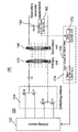
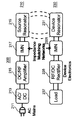
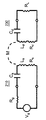
- FIG. 1 is a block diagram showing the configuration of the main part of one embodiment of a non-contact power transmission apparatus 100 according to the present invention.
- the primary side includes a driving circuit 120 connected to a primary coil 110 via a capacitor Cc.
- the driving circuit 120 includes a driving means 122 and a switching means 124. It is configured.
- the switching means 124 is configured as a bridge circuit including transistor elements Q1 to Q4.
- the secondary side includes a secondary coil 140 that is spaced apart from the primary coil 110 by a coupling coefficient k, and a resonance capacitor (Cp) 150 that is coupled to the secondary coil 140 to form a resonance circuit.
- Resonance current phase detection means 160 for detecting phase information of the resonance current flowing through the resonance capacitor (Cp) 150.
- the present invention includes phase information transmission means 170 that transmits phase information detected by the resonance current phase detection means 160 to the drive circuit 120 without phase delay, and the drive circuit 120 determines a drive frequency based on this phase information.
- the phase information transmission unit 170 includes a phase information transmitter 172 and a phase information receiver 174.
- the secondary side is connected to a load (not shown).
- the resonance circuit is only a resonance circuit configured by coupling the resonance capacitor (Cp) 150 to the secondary coil 140, and no positive series resonance capacitor is provided in the primary coil 110.
- the capacitor Cc shown in FIG. 1 is provided only for the purpose of blocking direct current, and is not provided as a resonant capacitor. More specifically, when the capacitance of this capacitor is set to be small in consideration of cost and the like, it may be slightly involved in the resonance on the primary side, but this is not an essential resonance. Further, the capacitor Cc can be omitted if the drive timing of the switching means 124 can be precisely controlled and the balance of the currents flowing through the transistor elements Q1 to Q4 can be maintained.
- the phase information of the resonance current flowing in the resonance circuit composed of the secondary coil 140 and the resonance capacitor (Cp) 150 connected in parallel or in series is detected by the resonance current phase detection means 160, and the phase is detected.
- Information is sent from the phase information transmitting means 172 on the secondary side to the phase information receiving means 174 on the primary side, and the driving timing of the driving means 122 is determined based on the phase information.
- the resonance circuit since the resonance circuit is not provided on the primary side, the number of turns of the primary coil 110 is different from that of a magnetic resonance method that requires a conventional primary side resonance circuit.
- the phase information transmission unit 170 transmits the phase information detected by the resonance current phase detection unit 160 "without phase delay", but any detection unit or transmission unit necessarily has a phase delay. Therefore, here, “without phase delay” means to make the phase delay as small as possible.
- the driving unit 122 Based on the phase information transmitted from the phase information transmitting unit 170, the driving unit 122 is configured so that the current phase of the driving current flowing through the primary coil 110 is slightly delayed from the voltage phase of the driving voltage applied to the primary coil 110.
- the drive frequency is determined and the switching means 124 is driven.
- the switching means 124 is composed of switching elements (Q1 to Q4) such as 2 or 4 transistors, and drives the primary coil 110 via a DC blocking capacitor Cc.
- FIG. 2 is a circuit diagram showing an example of the switching means 124, in which A indicates a full bridge circuit and B indicates a half bridge circuit.
- the switching means 124 may be a full bridge circuit or a half bridge circuit.
- the phase relationship between the drive voltage applied to the primary coil 110 and the drive current flowing through the primary coil 110 as viewed from the switching means 124 side varies greatly depending on the drive frequency, and therefore under various conditions. It was difficult to keep ZVS and prevent hard switching. Therefore, a full bridge circuit has been favorably used because abnormal voltages are unlikely to occur even when hard switching occurs.
- a half-bridge circuit which is said to be difficult due to hard switching, can be employed with peace of mind. This is because in the present invention, ZVS can be maintained under various conditions. Details will be described later.
- the full bridge circuit has only the advantage that the utilization efficiency of the power supply is high, and is not an essential condition in the present invention. Therefore, a case where a full bridge circuit is used as the switching means 124 will be described below.
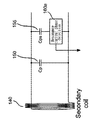
- FIG. 3 is a diagram showing a configuration of a detection unit including the resonance current phase detection means 160 of the present invention.
- a resonant capacitor (Cp) 150 and a small-capacitance capacitor (Cps) 155 are connected to the secondary coil 140 in parallel.
- the resonance current detection means 160 may detect the phase information of the current flowing directly through the resonance capacitor (Cp) 150 as shown in FIG. 1, or may be a small size connected in parallel as shown in FIG. It may be one (160a) that detects phase information of the current flowing through the capacitor (Cps) 155.
- the resonance current detection means 160 must be composed of a large capacity component. If the current flowing in (Cps) is detected, it can be constituted by a small capacity component.
- the phase information of the resonance current detected by the resonance current phase detection unit 160 is transmitted to the drive circuit 120 on the primary side by the resonance current phase transmission unit 170.
- the resonance current phase transmission means 170 are conceivable, but optical coupling using an LED and a phototransistor may be used, and the magnetic circuit is modulated and transmitted by a signal obtained by digitizing phase information.
- a wireless means using an electromagnetic wave of a high frequency carrier may be used.
- a phototransistor is used as the light receiving portion, the delay due to the accumulated charge is large, and means for saturating the phototransistor is not preferable.
- the phototransistor preferably has a non-saturated operation, and more preferably has a constant voltage operation for suppressing the mirror effect. It is more preferable to use a Pin photodiode or to use it with a reverse bias to achieve high-speed operation.
- the resonance current phase detection means 160 may be one (160b) that detects a current flowing through the secondary coil 140 as shown in FIG. In this case, however, the detected phase information is combined with the phase component of the current flowing through the load. Since the phase component of the current flowing through the load is delayed by 90 ° from the resonance current phase, these vectors are combined to cause a slight phase delay in the phase information.
- the primary coil 110 is driven based on this phase information, the ZVS operation is lost and hard switching is likely to occur.
- hard switching occurs, high-frequency parasitic vibrations occur in the elements (Q1 to Q4) of the switching means 124.
- EMI Electro-Magnetic Interference
- noise power / noise electric field strength (radiation) Will increase. Therefore, countermeasures are required, which will be described later.
- the resonance current phase detection means 160 may be one (160c) that detects the current flowing through the primary coil 110 as shown in FIG. In this case, since hard switching occurs in many cases, it is necessary to separately correct the phase, which will be described later. Further, there is a case where the detected resonance current is distorted as a cause of delay of the resonance current phase information. Such distortion causes the resonance current phase information to be distorted, the drive timing of the primary coil 110 becomes inaccurate, and the peak of the resonance frequency cannot be detected correctly.
- FIG. 6 is an example of a case where the resonant current includes a third-order high frequency, and is an explanatory diagram for explaining that the phase information is distorted due to this distortion.
- the phase information it is possible to improve the accuracy of the phase information by taking out only the basic component by using an appropriate filter means and using it as the resonance current phase information.
- FIG. 7 is a conceptual diagram showing that the resonance current phase detection means 160 is provided with a filter (Fundamental wave filter) 165 for extracting only the fundamental wave to remove harmonic distortion from the resonance current phase waveform.
- a filter Frundamental wave filter
- Non-contact power transmission is greatly different from power supply by a general leakage transformer.
- the coupling coefficient (k) between the primary coil and the secondary coil is almost constant under all driving conditions, whereas the coupling coefficient (k) varies greatly in non-contact power transmission.
- the Q value of the secondary side resonance circuit does not need to be so high.
- the coupling coefficient (k) changes in the case of non-contact power transmission, a high Q value is required when the coupling coefficient (k) is small.
- the phase delay (or time delay) in the means for transmitting the resonance current phase information must be minimized.
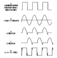
- FIG. 8 is a conceptual diagram showing changes in various waveforms when a phase delay occurs in the resonance current phase information.
- a is the waveform of the resonance current of the resonance circuit
- b is the waveform of the phase information detected by the resonance current phase detection means 160
- c is the waveform of the phase information output from the phase information reception means 174
- d is flowing through the primary coil 11. It is a current waveform of current.
- the waveform c output from the phase information receiving unit 174 becomes the driving waveform of the switching unit 124 almost as it is.
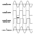
- FIG. 9 is a diagram showing a waveform of a current flowing through the switching means 124 when the ZVS operation is performed when the phase delay of the resonance current phase information is small.
- the waveform of the phase information receiving unit 174 has no delay or is extremely small (c)
- the timing of the current flowing through the primary coil 110 is slightly earlier than the switching timing of the switching unit 124 (d )
- the current waveforms (e, f) of the switching elements Q1, Q2 of the switching means 124 are ZVS operations.
- the center tap voltage of the switching means 124 is a clean square wave (g).
- FIG. 10 is a diagram showing a waveform of a current flowing through the switching means 124 when the ZVS operation is not performed when the phase delay of the resonance current phase information is large.
- the timing of the current flowing through the primary coil 110 is delayed (d), so that the current waveforms (e, f) of the switching elements Q1, Q2 do not perform the ZVS operation, and the switching means 124
- a characteristic pulse waveform due to rebound occurs in the center tap voltage of (g).
- the switching elements Q1 and Q2 and the driving means 122 may be destroyed, or EMI may be generated.
- the phase delay in the phase information transmission means 170 must be minimized. If phase delay is unavoidable, the following phase correction means is used.
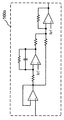
- FIG. 11 is a diagram illustrating an example of a circuit for correcting the phase of the resonance current phase information.
- the resonance current waveform detection circuit 162 in the resonance current phase detection means 160 and the inverted integration circuit 164 that inverts and integrates or integrates the detected resonance current waveform and the output from the resonance current waveform detection circuit 162 and the inversion integration.
- An adder circuit 166 that superimposes and combines the outputs from the circuit 164 is provided.
- the corrected resonance current phase information is obtained by detecting the phase information of the resonance current based on the waveform obtained by superimposing the waveform of the original resonance current and the waveform obtained by inverting and integrating the waveform. be able to. Then, this is sent to the phase information transmission means 170.
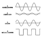
- FIG. 12 is a diagram for explaining the correction of the phase information described above.
- a is the original resonance current waveform information
- b is the inverse integration of this.
- c is a composite waveform obtained by superimposing a and b.
- the phase information d thus corrected has a waveform that transmits the original resonance current waveform information a without delay.
- the inverting integration circuit 164 can be configured using an operational amplifier (op-amp), or can be configured to integrate using a capacitor (C) and a resistor (R) after being inverted using a transformer. .
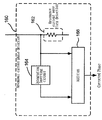
- FIG. 13 is a diagram showing a specific circuit diagram of the resonance current phase detection means 160a when performing phase correction.
- FIG. 14 is a diagram showing another specific circuit diagram of the resonance current phase detection means 160b. Focusing on the fact that the voltage across the resonance capacitor has an integrated waveform, the phase is corrected by inverting this. It is a thing.
- FIG. 15 is a diagram showing still another specific circuit diagram of the resonance current phase detection means 160c.
- the phase correction is performed by synthesizing the resonance current waveform detected from the primary coil 110 and its inverted integral waveform. It is also possible to use a differential waveform instead of integration without inversion. However, in many cases, the harmonic waveform is emphasized and superimposed on the differential waveform, which is not preferable as compared with the case where the integrated waveform is used. In the above description, the case where the resonance current waveform information and the resonance current phase information are handled in an analog manner has been described, but it goes without saying that the processing can be performed digitally based on these findings.
- the coupling coefficient (k) changes. Therefore, when the coupling coefficient (k) is low, a particularly large Q value is required for the resonance circuit.
- the primary coil satisfies the condition that the current phase of the drive current flowing through the primary coil is slightly delayed from the voltage phase of the drive voltage applied to the primary coil. Is difficult to drive.
- the drive frequency is fixed (so-called a fixed frequency method or a separate excitation method).
- the resonance current flowing in the resonance capacitor of the secondary side resonance circuit, the resonance current flowing in the secondary coil Alternatively, it is essential to control the drive circuit based on the phase information of the resonance current reflected in the primary coil. As a result, the drive frequency must be variable.
- Patent Document 1 discloses that the driving frequency is changed in accordance with the resistance component of the load in the magnetic resonance type non-contact power transmission.
- the driving means is driven by obtaining the optimum driving frequency by pre-programmed prediction information or calculation and saturable inductor by detecting the load resistance.
- the power factor seen from the switching means of the drive circuit for driving the primary coil since the power factor seen from the switching means of the drive circuit for driving the primary coil only approaches 1, and the power factor seen from the primary coil does not approach 1, the heat generation of the switching means is suppressed.
- the power factor seen from the side of the primary coil is very bad, causing the primary coil to generate heat.
- the setting of the Q value of the resonance circuit on the secondary coil side is set higher than usual.
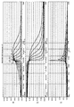
- FIG. 16 is a diagram for explaining the relationship between the current phase of the resonant capacitor coupled to the secondary coil and the current phase of the primary coil.
- the Q value required when the coupling coefficient (k) is changed is obtained by simulation. It is a thing.
- a is the current phase of the primary coil, the vertical axis is the phase angle, and the horizontal axis is the drive frequency.
- b is the current phase of the secondary resonance capacitor, the vertical axis is the phase angle, and the horizontal axis is the drive frequency.
- c is the transmission ratio, the vertical axis is the transmission ratio, and the horizontal axis is the drive frequency. If the transmission ratio is multiplied by the ratio between the number of turns of the primary coil and the number of turns of the secondary coil, the transmission ratio is approximately the boost ratio.
- the coupling coefficient (k) When the coupling coefficient (k) is 0.5, the condition that the phase of the current flowing in the primary coil is slightly delayed from the phase of the drive voltage of the drive circuit that drives the primary coil by setting the Q value to 8 or more. You can see that it meets.
- the frequency at which the transmission ratio is highest is 85 kHz. At this frequency, the delay angle of the current flowing through the primary coil is 25 deg. Or less, and cos ⁇ , that is, the power factor is 0.9 or more, so 85 kHz can be said to be the optimum driving frequency.
- the phase of the resonant current flowing through the secondary side resonant capacitor is 0 deg. That is, if this resonance current phase information is transmitted to the drive circuit through the phase information transmission means without phase delay and the drive circuit is driven, the switching means can be automatically driven at the optimum drive frequency. Further, since this switching condition is also a ZVS operation, a stable ZVS operation is possible even if the switching means is a half-bridge configuration.
- the drive circuit is driven at the drive frequency determined based on the phase information of the resonance current, and the ZVS operation is automatically performed.
- the ZVS operation is not performed, and phase correction is necessary.
- the Q value of the resonance circuit is determined as follows by the leakage inductance (L) of the secondary coil, the capacitance (C) of the resonance capacitor, and the equivalent load resistance (R) on the secondary coil side.
- both the series connection and the parallel connection can be used for the connection between the secondary coil and the resonant capacitor.
- an example of the parallel connection will be described.
- a resonance circuit in which a resonance capacitor is provided in parallel with a secondary coil which is one of the present invention, is a series of resonant resonances when viewed from the drive side and a parallel resonance when viewed from the load side. That's why. This is called Parallel Loaded Serial Resonance or various names.
- parallel resonance is applied to the calculation formula of Q.
- the capacitance C of the resonance capacitor is made larger than the equivalent load resistance R, and the leakage inductance L of the secondary coil is made smaller.
- the definition of the leakage inductance L sc in the present invention is determined by the following equation.
- L 2 is the secondary coil inductance or the inductance of the independent third coil.
- Le as defined in (1) is a leakage inductance, and is not uniform.
- the resonance circuit configured on the secondary side by coupling the secondary coil and the resonance capacitor is connected to the secondary coil in parallel, in series, or in parallel to an independent third coil. Or any of those configured.
- a resonant circuit configured by connecting a third coil and a resonant capacitor will be described later.
- FIG. 17 is a diagram in which the minimum necessary Q value necessary for obtaining the power factor as seen from the primary coil is obtained by simulation.
- the horizontal axis is the drive frequency.
- a indicates the current phase of the primary coil with respect to the switching voltage of the primary coil
- b indicates the resonance current phase of the secondary side resonance capacitor
- c indicates the transmission ratio (transmission coefficient).
- the value of k 2 ⁇ Q gradually approaches 2 and does not exceed 2 as k decreases. This is because, in non-contact power transmission, when the distance between the primary coil and the secondary coil is large and the coupling coefficient k is sufficiently small, a secondary side resonance circuit for obtaining a power factor of 1 when viewed from the primary coil.
- the current phase curve of the primary coil must always cross the horizontal axis of 0 deg.
- the phase must cross so that it is positive, that is, capacitive to negative, that is, inductive.
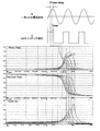
- FIG. 20 is a diagram illustrating an example of power control according to the present invention.
- a is the phase information of the resonance current
- b is the current waveform of the primary coil
- c and d are the gate control voltages when the switching means (Q2, Q1) are FETs, IGBTs or the like.
- the power control in the present invention is performed by turning on the switching means of the drive circuit for driving the primary coil and turning it off after a certain time based on the phase information of the resonance current.
- hard switching is generally a concern.
- the current phase of the primary coil is already behind the switching phase (see b). Since the phase is further delayed than the ON phase (see c and d), hard switching does not occur. At that time, since it is generally performed that a slight dead time (Dead time) is required so that (Q2, Q1) are not simultaneously turned ON, this is omitted in this description.
- FIG. 21 is a diagram illustrating another example of power control according to the present invention.
- the duty control side is only one of the switching means or one of the pair that is simultaneously turned on, and the other or the other pair is controlled by an inversion signal. At that time, a slight dead time is required on the side controlled by the inverted signal (see d).
- Such a control method is called non-uniform half-bridge or non-uniform full-bridge control. In this control method, even-order harmonic voltages are likely to be generated in the secondary coil.
- the Q value is set very high, there is no problem because the voltage of the secondary coil is almost close to a sine wave.
- FIG. 22 is a diagram for explaining the relationship with the current phase of the primary coil when the power control of the present invention is performed.
- the drive frequency when the control is performed is also increased.
- the ON phase of the drive voltage is further delayed than the phase of the phase information of the resonance current.
- the power factor is lowered, but at the same time, the transmission ratio is lowered, so that the controllable power range becomes very wide.
- a resonance circuit is configured by coupling a resonance capacitor to a secondary coil.
- the resonance on the secondary side as in the present invention is used.
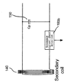
- the circuit is not essential. Therefore, a case will be described in which a third coil is provided in parallel with the secondary coil and a resonance capacitor is coupled to the third coil in order to apply the present invention while taking compatibility with the Qi standard.
- FIG. 23 is a diagram showing an example of a circuit that can improve efficiency while maintaining compatibility with the Qi standard.
- the third coil 190 may be provided as an independent coil close to the secondary coil 140. However, as shown in FIG. 23, the third coil 190 includes the secondary coil 140 as an autotransformer, and the voltage induced in the secondary coil 140 is increased. On the other hand, the third coil 190 may be wound in a relationship of increasing the pressure.
- a resonance capacitor (Cp) 150 is coupled to the third coil 190.
- the resonance capacitor (Cp) 150 is turned off by the switch 181.
- the resonance capacitor (Cp) 150 is turned on and Cp operates as the resonance capacitor 150.
- the switch 183 on the secondary coil 140 side is turned off and the switch 185 is turned on.
- the switch 181 is turned on, the Q value of the resonance circuit increases.
- the resonance current waveform detected by the resonance current phase detection means 160c provided on the primary side and its inverted integral waveform are combined to produce a phase. Correction may be performed and the driving circuit of the high frequency power source may be driven based on the resonance current phase information.
- the switches 181, 183, and 185 use FETs or transistors via diodes. However, any element can be used as long as it is an element capable of switching operation.
- the resonance current is inversely proportional to the number of turns, so the copper loss is also reduced in proportion to the square of the current. Heat generation can be reduced and efficiency is improved.
- Non-contact electric power transmission apparatus 110 Primary coil 120 Drive circuit 122 Driving means 124 Switching means 140 Secondary coil 150 Resonance capacitor 155 Small capacity capacitor 160 Resonant current phase detection means 165 Filter 170 Phase information transmission means 190 Third coil
Priority Applications (21)
| Application Number | Priority Date | Filing Date | Title |
|---|---|---|---|
| PCT/JP2014/002552 WO2015173847A1 (ja) | 2014-05-14 | 2014-05-14 | 非接触電力伝送装置 |
| BR112016026649A BR112016026649A2 (pt) | 2014-05-14 | 2014-09-19 | Sistema de transferência de potência sem fio |
| CN201910418086.2A CN110048524B (zh) | 2014-05-14 | 2014-09-19 | 无线电力传送装置 |
| EP19175476.1A EP3561997B1 (en) | 2014-05-14 | 2014-09-19 | Wireless power transfer system |
| KR1020167031783A KR102209812B1 (ko) | 2014-05-14 | 2014-09-19 | 무선 전력 전송 장치 |
| JP2016518656A JP6240755B2 (ja) | 2014-05-14 | 2014-09-19 | ワイヤレス電力伝送装置 |
| PCT/JP2014/004827 WO2015173850A1 (ja) | 2014-05-14 | 2014-09-19 | ワイヤレス電力伝送装置 |
| EP14891694.3A EP3145047B1 (en) | 2014-05-14 | 2014-09-19 | Wireless power transfer device |
| EP18207449.2A EP3487038B1 (en) | 2014-05-14 | 2014-09-19 | Wireless power transfer system |
| US15/310,222 US10243406B2 (en) | 2014-05-14 | 2014-09-19 | Wireless power transfer system |
| KR1020217002136A KR20210010673A (ko) | 2014-05-14 | 2014-09-19 | 무선 전력 전송 장치 |
| CN201910131824.5A CN109742870B (zh) | 2014-05-14 | 2014-09-19 | 无线电力传送装置 |
| CN201480079144.9A CN106471708B (zh) | 2014-05-14 | 2014-09-19 | 无线电力传送装置 |
| EP20216741.7A EP3826141B1 (en) | 2014-05-14 | 2014-09-19 | Wireless power transfer system |
| TW107134206A TWI702769B (zh) | 2014-05-14 | 2015-05-14 | 無線電力傳送裝置 |
| TW104115405A TWI667858B (zh) | 2014-05-14 | 2015-05-14 | 無線電力傳送裝置 |
| HK17104947.7A HK1231637A1 (zh) | 2014-05-14 | 2017-05-17 | 無線電力傳送裝置 |
| JP2017213795A JP6450822B2 (ja) | 2014-05-14 | 2017-11-06 | ワイヤレス電力伝送装置 |
| JP2018230511A JP6605690B2 (ja) | 2014-05-14 | 2018-12-10 | ワイヤレス電力伝送装置 |
| US16/351,332 US10547214B2 (en) | 2014-05-14 | 2019-03-12 | Wireless power transfer system |
| US16/717,317 US11005300B2 (en) | 2014-05-14 | 2019-12-17 | Wireless power transfer system |
Applications Claiming Priority (1)
| Application Number | Priority Date | Filing Date | Title |
|---|---|---|---|
| PCT/JP2014/002552 WO2015173847A1 (ja) | 2014-05-14 | 2014-05-14 | 非接触電力伝送装置 |
Publications (1)
| Publication Number | Publication Date |
|---|---|
| WO2015173847A1 true WO2015173847A1 (ja) | 2015-11-19 |
Family
ID=54479423
Family Applications (2)
| Application Number | Title | Priority Date | Filing Date |
|---|---|---|---|
| PCT/JP2014/002552 WO2015173847A1 (ja) | 2014-05-14 | 2014-05-14 | 非接触電力伝送装置 |
| PCT/JP2014/004827 WO2015173850A1 (ja) | 2014-05-14 | 2014-09-19 | ワイヤレス電力伝送装置 |
Family Applications After (1)
| Application Number | Title | Priority Date | Filing Date |
|---|---|---|---|
| PCT/JP2014/004827 WO2015173850A1 (ja) | 2014-05-14 | 2014-09-19 | ワイヤレス電力伝送装置 |
Country Status (9)
| Country | Link |
|---|---|
| US (3) | US10243406B2 (ko) |
| EP (4) | EP3487038B1 (ko) |
| JP (3) | JP6240755B2 (ko) |
| KR (2) | KR20210010673A (ko) |
| CN (3) | CN110048524B (ko) |
| BR (1) | BR112016026649A2 (ko) |
| HK (1) | HK1231637A1 (ko) |
| TW (2) | TWI702769B (ko) |
| WO (2) | WO2015173847A1 (ko) |
Families Citing this family (51)
| Publication number | Priority date | Publication date | Assignee | Title |
|---|---|---|---|---|
| WO2015173847A1 (ja) * | 2014-05-14 | 2015-11-19 | ネオテス株式会社 | 非接触電力伝送装置 |
| CN106716779B (zh) * | 2014-11-17 | 2019-04-02 | 株式会社村田制作所 | 无线供电装置 |
| US10186908B2 (en) * | 2015-08-04 | 2019-01-22 | Ningbo Weie Electronic Technology Co., Ltd. | Efficient power transmitting terminal, contactless power transmission device and power transmission method |
| CN109155191B (zh) | 2016-05-11 | 2020-11-03 | Ntn株式会社 | 相对旋转部的电传送装置 |
| KR101846954B1 (ko) * | 2016-06-13 | 2018-04-10 | 주식회사 맵스 | 임피던스 변화에 자동 조정 가능한 무선 전력 송신기 |
| US10985615B2 (en) * | 2016-06-28 | 2021-04-20 | Lg Innotek Co., Ltd. | Wireless power control method and device for wireless charging |
| CN107623344A (zh) * | 2016-07-15 | 2018-01-23 | 华为技术有限公司 | 无线充电电路、无线充电系统及电路控制方法 |
| CN106300065B (zh) * | 2016-09-22 | 2018-03-20 | 福州大学 | 基于无线取能操动机构的开关柜系统 |
| US11239699B2 (en) | 2017-04-05 | 2022-02-01 | Mbda Uk Limited | Inductive power transfer system |
| GB2561200B (en) * | 2017-04-05 | 2022-04-27 | Mbda Uk Ltd | Inductive power transfer system |
| US10693326B2 (en) | 2017-07-27 | 2020-06-23 | Electronics And Telecommunications Research Institute | Wireless power receiving apparatus controlling effective load resistance, and effective load resistance control method |
| JP7044505B2 (ja) * | 2017-09-14 | 2022-03-30 | マクセル株式会社 | 非接触電力伝送装置、送電装置、および、受電装置 |
| CN111247712B (zh) * | 2017-09-17 | 2024-01-16 | 毛恒春 | 模块化高效无线功率传输系统 |
| CN108318738B (zh) * | 2018-01-26 | 2020-06-12 | 上海交通大学 | 一种无线电能传输系统的相位检测电路以及参数信息检测方法 |
| US10908200B2 (en) * | 2018-03-29 | 2021-02-02 | Cirrus Logic, Inc. | Resonant phase sensing of resistive-inductive-capacitive sensors |
| US10642435B2 (en) | 2018-03-29 | 2020-05-05 | Cirrus Logic, Inc. | False triggering prevention in a resonant phase sensing system |
| US11537242B2 (en) | 2018-03-29 | 2022-12-27 | Cirrus Logic, Inc. | Q-factor enhancement in resonant phase sensing of resistive-inductive-capacitive sensors |
| US11092657B2 (en) | 2018-03-29 | 2021-08-17 | Cirrus Logic, Inc. | Compensation of changes in a resonant phase sensing system including a resistive-inductive-capacitive sensor |
| KR102544616B1 (ko) * | 2018-04-10 | 2023-06-19 | 삼성전자주식회사 | 무선 전력 전송 시스템 및 그 시스템을 포함하는 디스플레이 장치 |
| US11005298B2 (en) * | 2018-08-29 | 2021-05-11 | Integrated Device Technology, Inc. | Wireless power maximum efficiency tracking by system control |
| US11017942B2 (en) | 2018-11-01 | 2021-05-25 | Witricity Corporation | Systems and methods for determining coil current in wireless power systems |
| KR102160960B1 (ko) * | 2018-11-13 | 2020-09-29 | 엘지전자 주식회사 | 무선 전력 송수신 장치, 및 이 장치를 포함하는 홈 어플라이언스 |
| KR102605636B1 (ko) * | 2018-11-20 | 2023-11-22 | 엘지전자 주식회사 | 하이브리드 동기 정류기 |
| CN114928177A (zh) | 2018-11-30 | 2022-08-19 | 韦特里西提公司 | 用于高功率无线功率系统中的低功率激励的系统和方法 |
| JP7131344B2 (ja) | 2018-12-03 | 2022-09-06 | オムロン株式会社 | 非接触給電装置 |
| CN109672343B (zh) * | 2018-12-17 | 2020-12-18 | 华为技术有限公司 | 一种接收端的相位校准电路、方法及接收端 |
| US10948313B2 (en) | 2019-02-26 | 2021-03-16 | Cirrus Logic, Inc. | Spread spectrum sensor scanning using resistive-inductive-capacitive sensors |
| US11402946B2 (en) | 2019-02-26 | 2022-08-02 | Cirrus Logic, Inc. | Multi-chip synchronization in sensor applications |
| US11536758B2 (en) | 2019-02-26 | 2022-12-27 | Cirrus Logic, Inc. | Single-capacitor inductive sense systems |
| CN113614553B (zh) * | 2019-03-13 | 2023-10-24 | 三菱电机株式会社 | 触点部异常监视装置及使用该装置的电路断路器 |
| US11695271B2 (en) | 2019-05-24 | 2023-07-04 | Witricity Corporation | Protection circuits for wireless power receivers |
| WO2021041574A1 (en) | 2019-08-26 | 2021-03-04 | Witricity Corporation | Control of active rectification in wireless power systems |
| JP7408952B2 (ja) | 2019-08-28 | 2024-01-09 | オムロン株式会社 | 非接触給電装置 |
| JP7395879B2 (ja) * | 2019-08-28 | 2023-12-12 | オムロン株式会社 | 非接触給電装置及び送電装置 |
| WO2021044348A1 (en) * | 2019-09-03 | 2021-03-11 | Auckland Uniservices Limited | Inductive power transfer system control |
| EP4094344A1 (en) | 2020-01-23 | 2022-11-30 | WiTricity Corporation | Tunable reactance circuits for wireless power systems |
| US11695270B2 (en) | 2020-01-29 | 2023-07-04 | Witricity Corporation | Systems and methods for auxiliary power dropout protection |
| CN115244816A (zh) | 2020-03-06 | 2022-10-25 | 韦特里西提公司 | 无线电力系统中的有源整流 |
| US11579030B2 (en) | 2020-06-18 | 2023-02-14 | Cirrus Logic, Inc. | Baseline estimation for sensor system |
| US11868540B2 (en) | 2020-06-25 | 2024-01-09 | Cirrus Logic Inc. | Determination of resonant frequency and quality factor for a sensor system |
| US11835410B2 (en) | 2020-06-25 | 2023-12-05 | Cirrus Logic Inc. | Determination of resonant frequency and quality factor for a sensor system |
| CN111900943B (zh) * | 2020-07-14 | 2023-05-05 | 电子科技大学 | 一种射频宽带高效率整流器 |
| CN112600315B (zh) * | 2020-11-17 | 2022-11-18 | 华南理工大学 | 输出与各负载无关的多恒压输出无线输电系统构造方法 |
| TWI759972B (zh) * | 2020-11-25 | 2022-04-01 | 偉詮電子股份有限公司 | 無線功率傳輸系統之快速異物檢測方法與相關之無線功率發送模組 |
| US11619519B2 (en) | 2021-02-08 | 2023-04-04 | Cirrus Logic, Inc. | Predictive sensor tracking optimization in multi-sensor sensing applications |
| US11808669B2 (en) | 2021-03-29 | 2023-11-07 | Cirrus Logic Inc. | Gain and mismatch calibration for a phase detector used in an inductive sensor |
| US11821761B2 (en) | 2021-03-29 | 2023-11-21 | Cirrus Logic Inc. | Maximizing dynamic range in resonant sensing |
| US11507199B2 (en) | 2021-03-30 | 2022-11-22 | Cirrus Logic, Inc. | Pseudo-differential phase measurement and quality factor compensation |
| US11854738B2 (en) | 2021-12-02 | 2023-12-26 | Cirrus Logic Inc. | Slew control for variable load pulse-width modulation driver and load sensing |
| IT202100031289A1 (it) * | 2021-12-14 | 2023-06-14 | Gebat S R L | Circuito monitor di risonanza per trasferimento induttivo di energia, e relativo sistema di trasferimento induttivo ottimizzato di energia elettrica |
| CN117040144A (zh) * | 2023-09-12 | 2023-11-10 | 重庆大学 | Bcpt系统的频率调谐及功率流解耦控制方法和系统 |
Citations (4)
| Publication number | Priority date | Publication date | Assignee | Title |
|---|---|---|---|---|
| JP2008125198A (ja) * | 2006-11-09 | 2008-05-29 | Ishida Co Ltd | 非接触給電装置 |
| WO2012090700A1 (ja) * | 2010-12-28 | 2012-07-05 | Tdk株式会社 | ワイヤレス給電装置、ワイヤレス受電装置、ワイヤレス伝送システム |
| JP2013153627A (ja) * | 2012-01-26 | 2013-08-08 | Shindengen Electric Mfg Co Ltd | 非接触給電回路 |
| JP2014033516A (ja) * | 2012-08-02 | 2014-02-20 | Toyota Motor Corp | 非接触送電装置、非接触受電装置、車両および非接触送受電システム |
Family Cites Families (46)
| Publication number | Priority date | Publication date | Assignee | Title |
|---|---|---|---|---|
| JPS4921466B1 (ko) | 1970-10-24 | 1974-06-01 | ||
| JPS5111666B2 (ko) | 1972-06-19 | 1976-04-13 | ||
| JPS5525268B2 (ko) | 1975-02-03 | 1980-07-04 | ||
| EP0253345B1 (en) | 1986-07-18 | 1992-10-21 | Inductran Corporation | Inductive power coupling with constant voltage output |
| US7522878B2 (en) * | 1999-06-21 | 2009-04-21 | Access Business Group International Llc | Adaptive inductive power supply with communication |
| US6301128B1 (en) * | 2000-02-09 | 2001-10-09 | Delta Electronics, Inc. | Contactless electrical energy transmission system |
| JP2002272134A (ja) | 2001-03-08 | 2002-09-20 | Mitsubishi Heavy Ind Ltd | 高周波電力の非接触給電装置及び非接触給電方法 |
| JP3738019B2 (ja) * | 2003-09-04 | 2006-01-25 | Tdk株式会社 | スイッチング電源装置用制御装置及びスイッチング電源装置 |
| JP4207916B2 (ja) * | 2004-03-30 | 2009-01-14 | 株式会社ダイフク | 無接触給電設備 |
| EP2306616B2 (en) | 2005-07-12 | 2023-06-21 | Massachusetts Institute of Technology (MIT) | Wireless non-radiative energy transfer |
| US7382636B2 (en) * | 2005-10-14 | 2008-06-03 | Access Business Group International Llc | System and method for powering a load |
| KR101356409B1 (ko) | 2007-03-27 | 2014-01-27 | 메사추세츠 인스티튜트 오브 테크놀로지 | 무선 에너지 전달 |
| JP2009130389A (ja) * | 2007-11-19 | 2009-06-11 | Felica Networks Inc | 通信装置、同調周波数調整方法、およびプログラム |
| JP4561886B2 (ja) * | 2008-06-27 | 2010-10-13 | ソニー株式会社 | 電力伝送装置、給電装置及び受電装置 |
| US8923015B2 (en) * | 2008-11-26 | 2014-12-30 | Auckland Uniservices Limited | Primary-side power control for inductive power transfer |
| US20100276995A1 (en) | 2009-04-29 | 2010-11-04 | Thomas Louis Marzetta | Security for wireless transfer of electrical power |
| CN102013736B (zh) * | 2009-09-03 | 2013-10-16 | Tdk株式会社 | 无线馈电装置和无线电力传输系统 |
| JP5993304B2 (ja) * | 2009-09-09 | 2016-09-14 | オークランド ユニサービシズ リミテッドAuckland Uniservices Limited | 誘導電力伝送システムにおける電力需要管理 |
| JP5506327B2 (ja) | 2009-10-27 | 2014-05-28 | 株式会社ヘッズ | 非接触電力供給装置 |
| JP5664018B2 (ja) * | 2009-10-30 | 2015-02-04 | Tdk株式会社 | ワイヤレス給電装置、ワイヤレス電力伝送システムおよびそれらを利用したテーブルと卓上ランプ |
| US8729735B2 (en) * | 2009-11-30 | 2014-05-20 | Tdk Corporation | Wireless power feeder, wireless power receiver, and wireless power transmission system |
| KR101438294B1 (ko) * | 2010-02-10 | 2014-09-04 | 후지쯔 가부시끼가이샤 | 자계 공명형 전력 전송 시스템에 있어서의 공진 주파수 제어 방법, 송전 장치, 및 수전 장치 |
| CN101834473B (zh) * | 2010-05-21 | 2012-05-09 | 西安电子科技大学 | 谐振跟踪式非接触供电装置及供电方法 |
| JP2012110199A (ja) * | 2010-10-27 | 2012-06-07 | Equos Research Co Ltd | 電力伝送システム |
| US20120146424A1 (en) * | 2010-12-14 | 2012-06-14 | Takashi Urano | Wireless power feeder and wireless power transmission system |
| US20120169131A1 (en) * | 2010-12-29 | 2012-07-05 | Choudhary Vijay N | Phase shift power transfer |
| WO2012101907A1 (ja) * | 2011-01-26 | 2012-08-02 | 株式会社村田製作所 | 電力伝送システム |
| JP5843309B2 (ja) * | 2011-02-24 | 2016-01-13 | 国立大学法人東北大学 | 非接触電力伝送システム |
| US8742627B2 (en) * | 2011-03-01 | 2014-06-03 | Tdk Corporation | Wireless power feeder |
| JP5677875B2 (ja) * | 2011-03-16 | 2015-02-25 | 日立マクセル株式会社 | 非接触電力伝送システム |
| JP5840886B2 (ja) * | 2011-07-25 | 2016-01-06 | ソニー株式会社 | 検知装置、受電装置、送電装置、非接触電力伝送システム及び検知方法 |
| JP2013046561A (ja) * | 2011-08-26 | 2013-03-04 | Toshiba Corp | 送電装置 |
| WO2013042224A1 (ja) * | 2011-09-21 | 2013-03-28 | パイオニア株式会社 | 非接触電力送電装置、非接触電力受電装置、及び非接触給電システム |
| JP5988191B2 (ja) * | 2011-09-27 | 2016-09-07 | 株式会社エクォス・リサーチ | 電力伝送システム |
| US9356474B2 (en) * | 2011-09-28 | 2016-05-31 | Tdk Corporation | Wireless power feeder and wireless power transmission system |
| US8934424B2 (en) * | 2011-09-29 | 2015-01-13 | Sharp Laboratories Of America, Inc. | Devices for reconfiguring a subframe allocation |
| JP6099020B2 (ja) * | 2011-12-14 | 2017-03-22 | パナソニックIpマネジメント株式会社 | 情報伝送装置及びシステム |
| EP2827471B1 (en) * | 2012-03-13 | 2018-05-23 | Pioneer Corporation | Power-receiving device and power-receiving method |
| US20130270919A1 (en) | 2012-04-16 | 2013-10-17 | Ut-Battelle, Llc | Above resonance frequency operation for wireless power transfer |
| JP2014024365A (ja) * | 2012-07-24 | 2014-02-06 | Railway Technical Research Institute | 非接触給電システム |
| US10506454B2 (en) | 2012-07-31 | 2019-12-10 | Dali Systems Co., Ltd. | Optimization of traffic load in a distributed antenna system |
| JP6382818B2 (ja) * | 2012-09-11 | 2018-08-29 | フィリップス アイピー ベンチャーズ ビー ヴィ | 無線電力制御 |
| US9596358B2 (en) | 2012-09-21 | 2017-03-14 | Oncept, Inc | System and method for corporate mobile subscription management |
| US20140084688A1 (en) * | 2012-09-21 | 2014-03-27 | Samsung Electronics Co. Ltd | Method and apparatus for wireless power transmission |
| KR101601352B1 (ko) * | 2012-09-26 | 2016-03-08 | 엘지이노텍 주식회사 | 무선전력 송신장치 및 그의 전력 제어 방법 |
| WO2015173847A1 (ja) * | 2014-05-14 | 2015-11-19 | ネオテス株式会社 | 非接触電力伝送装置 |
-
2014
- 2014-05-14 WO PCT/JP2014/002552 patent/WO2015173847A1/ja active Application Filing
- 2014-09-19 KR KR1020217002136A patent/KR20210010673A/ko active IP Right Grant
- 2014-09-19 JP JP2016518656A patent/JP6240755B2/ja active Active
- 2014-09-19 US US15/310,222 patent/US10243406B2/en active Active
- 2014-09-19 CN CN201910418086.2A patent/CN110048524B/zh active Active
- 2014-09-19 KR KR1020167031783A patent/KR102209812B1/ko active IP Right Grant
- 2014-09-19 EP EP18207449.2A patent/EP3487038B1/en active Active
- 2014-09-19 EP EP14891694.3A patent/EP3145047B1/en active Active
- 2014-09-19 WO PCT/JP2014/004827 patent/WO2015173850A1/ja active Application Filing
- 2014-09-19 EP EP20216741.7A patent/EP3826141B1/en active Active
- 2014-09-19 EP EP19175476.1A patent/EP3561997B1/en active Active
- 2014-09-19 CN CN201480079144.9A patent/CN106471708B/zh active Active
- 2014-09-19 BR BR112016026649A patent/BR112016026649A2/pt not_active Application Discontinuation
- 2014-09-19 CN CN201910131824.5A patent/CN109742870B/zh active Active
-
2015
- 2015-05-14 TW TW107134206A patent/TWI702769B/zh active
- 2015-05-14 TW TW104115405A patent/TWI667858B/zh active
-
2017
- 2017-05-17 HK HK17104947.7A patent/HK1231637A1/zh unknown
- 2017-11-06 JP JP2017213795A patent/JP6450822B2/ja active Active
-
2018
- 2018-12-10 JP JP2018230511A patent/JP6605690B2/ja active Active
-
2019
- 2019-03-12 US US16/351,332 patent/US10547214B2/en active Active
- 2019-12-17 US US16/717,317 patent/US11005300B2/en active Active
Patent Citations (4)
| Publication number | Priority date | Publication date | Assignee | Title |
|---|---|---|---|---|
| JP2008125198A (ja) * | 2006-11-09 | 2008-05-29 | Ishida Co Ltd | 非接触給電装置 |
| WO2012090700A1 (ja) * | 2010-12-28 | 2012-07-05 | Tdk株式会社 | ワイヤレス給電装置、ワイヤレス受電装置、ワイヤレス伝送システム |
| JP2013153627A (ja) * | 2012-01-26 | 2013-08-08 | Shindengen Electric Mfg Co Ltd | 非接触給電回路 |
| JP2014033516A (ja) * | 2012-08-02 | 2014-02-20 | Toyota Motor Corp | 非接触送電装置、非接触受電装置、車両および非接触送受電システム |
Also Published As
Similar Documents
| Publication | Publication Date | Title |
|---|---|---|
| JP6605690B2 (ja) | ワイヤレス電力伝送装置 | |
| US10483810B2 (en) | Variable-distance wireless-power-transfer system with fixed tuning and power limiting | |
| CN109478871B (zh) | 二极管导通传感器 | |
| JP5640783B2 (ja) | ワイヤレス給電装置、ワイヤレス受電装置およびワイヤレス電力伝送システム | |
| US20240007062A1 (en) | High frequency wireless power transfer system, transmitter and receiver therefor | |
| WO2015063920A1 (ja) | 共振型高周波電源装置 | |
| US10110071B2 (en) | Resonance-type power transmitter | |
| US20210021156A1 (en) | True optimizable wireless power systems | |
| JP2011176973A (ja) | 共振型スイッチング電源装置 | |
| KR20170125101A (ko) | 유도식 전력 수신기 | |
| JP2019017151A (ja) | 高周波電源装置及び送電装置 | |
| JPWO2015063921A1 (ja) | 共振型高周波電源装置 |
Legal Events
| Date | Code | Title | Description |
|---|---|---|---|
| 121 | Ep: the epo has been informed by wipo that ep was designated in this application |
Ref document number: 14892216 Country of ref document: EP Kind code of ref document: A1 |
|
| NENP | Non-entry into the national phase |
Ref country code: DE |
|
| 122 | Ep: pct application non-entry in european phase |
Ref document number: 14892216 Country of ref document: EP Kind code of ref document: A1 |
|
| NENP | Non-entry into the national phase |
Ref country code: JP |