WO2015159481A1 - 半導体基板及び半導体素子 - Google Patents
半導体基板及び半導体素子 Download PDFInfo
- Publication number
- WO2015159481A1 WO2015159481A1 PCT/JP2015/001371 JP2015001371W WO2015159481A1 WO 2015159481 A1 WO2015159481 A1 WO 2015159481A1 JP 2015001371 W JP2015001371 W JP 2015001371W WO 2015159481 A1 WO2015159481 A1 WO 2015159481A1
- Authority
- WO
- WIPO (PCT)
- Prior art keywords
- layer
- region
- semiconductor substrate
- semiconductor
- carbon
- Prior art date
- Legal status (The legal status is an assumption and is not a legal conclusion. Google has not performed a legal analysis and makes no representation as to the accuracy of the status listed.)
- Ceased
Links
Images


Classifications
-
- H—ELECTRICITY
- H10—SEMICONDUCTOR DEVICES; ELECTRIC SOLID-STATE DEVICES NOT OTHERWISE PROVIDED FOR
- H10D—INORGANIC ELECTRIC SEMICONDUCTOR DEVICES
- H10D30/00—Field-effect transistors [FET]
- H10D30/40—FETs having zero-dimensional [0D], one-dimensional [1D] or two-dimensional [2D] charge carrier gas channels
- H10D30/47—FETs having zero-dimensional [0D], one-dimensional [1D] or two-dimensional [2D] charge carrier gas channels having two-dimensional [2D] charge carrier gas channels, e.g. nanoribbon FETs or high electron mobility transistors [HEMT]
- H10D30/471—High electron mobility transistors [HEMT] or high hole mobility transistors [HHMT]
- H10D30/475—High electron mobility transistors [HEMT] or high hole mobility transistors [HHMT] having wider bandgap layer formed on top of lower bandgap active layer, e.g. undoped barrier HEMTs such as i-AlGaN/GaN HEMTs
-
- H—ELECTRICITY
- H10—SEMICONDUCTOR DEVICES; ELECTRIC SOLID-STATE DEVICES NOT OTHERWISE PROVIDED FOR
- H10D—INORGANIC ELECTRIC SEMICONDUCTOR DEVICES
- H10D30/00—Field-effect transistors [FET]
- H10D30/01—Manufacture or treatment
- H10D30/015—Manufacture or treatment of FETs having heterojunction interface channels or heterojunction gate electrodes, e.g. HEMT
-
- H—ELECTRICITY
- H10—SEMICONDUCTOR DEVICES; ELECTRIC SOLID-STATE DEVICES NOT OTHERWISE PROVIDED FOR
- H10D—INORGANIC ELECTRIC SEMICONDUCTOR DEVICES
- H10D62/00—Semiconductor bodies, or regions thereof, of devices having potential barriers
- H10D62/80—Semiconductor bodies, or regions thereof, of devices having potential barriers characterised by the materials
- H10D62/85—Semiconductor bodies, or regions thereof, of devices having potential barriers characterised by the materials being Group III-V materials, e.g. GaAs
- H10D62/8503—Nitride Group III-V materials, e.g. AlN or GaN
-
- H—ELECTRICITY
- H10—SEMICONDUCTOR DEVICES; ELECTRIC SOLID-STATE DEVICES NOT OTHERWISE PROVIDED FOR
- H10D—INORGANIC ELECTRIC SEMICONDUCTOR DEVICES
- H10D62/00—Semiconductor bodies, or regions thereof, of devices having potential barriers
- H10D62/80—Semiconductor bodies, or regions thereof, of devices having potential barriers characterised by the materials
- H10D62/85—Semiconductor bodies, or regions thereof, of devices having potential barriers characterised by the materials being Group III-V materials, e.g. GaAs
- H10D62/854—Semiconductor bodies, or regions thereof, of devices having potential barriers characterised by the materials being Group III-V materials, e.g. GaAs further characterised by the dopants
-
- H—ELECTRICITY
- H10—SEMICONDUCTOR DEVICES; ELECTRIC SOLID-STATE DEVICES NOT OTHERWISE PROVIDED FOR
- H10P—GENERIC PROCESSES OR APPARATUS FOR THE MANUFACTURE OR TREATMENT OF DEVICES COVERED BY CLASS H10
- H10P14/00—Formation of materials, e.g. in the shape of layers or pillars
- H10P14/20—Formation of materials, e.g. in the shape of layers or pillars of semiconductor materials
- H10P14/24—Formation of materials, e.g. in the shape of layers or pillars of semiconductor materials using chemical vapour deposition [CVD]
-
- H—ELECTRICITY
- H10—SEMICONDUCTOR DEVICES; ELECTRIC SOLID-STATE DEVICES NOT OTHERWISE PROVIDED FOR
- H10P—GENERIC PROCESSES OR APPARATUS FOR THE MANUFACTURE OR TREATMENT OF DEVICES COVERED BY CLASS H10
- H10P14/00—Formation of materials, e.g. in the shape of layers or pillars
- H10P14/20—Formation of materials, e.g. in the shape of layers or pillars of semiconductor materials
- H10P14/29—Formation of materials, e.g. in the shape of layers or pillars of semiconductor materials characterised by the substrates
-
- H—ELECTRICITY
- H10—SEMICONDUCTOR DEVICES; ELECTRIC SOLID-STATE DEVICES NOT OTHERWISE PROVIDED FOR
- H10P—GENERIC PROCESSES OR APPARATUS FOR THE MANUFACTURE OR TREATMENT OF DEVICES COVERED BY CLASS H10
- H10P14/00—Formation of materials, e.g. in the shape of layers or pillars
- H10P14/20—Formation of materials, e.g. in the shape of layers or pillars of semiconductor materials
- H10P14/29—Formation of materials, e.g. in the shape of layers or pillars of semiconductor materials characterised by the substrates
- H10P14/2901—Materials
- H10P14/2902—Materials being Group IVA materials
- H10P14/2904—Silicon carbide
-
- H—ELECTRICITY
- H10—SEMICONDUCTOR DEVICES; ELECTRIC SOLID-STATE DEVICES NOT OTHERWISE PROVIDED FOR
- H10P—GENERIC PROCESSES OR APPARATUS FOR THE MANUFACTURE OR TREATMENT OF DEVICES COVERED BY CLASS H10
- H10P14/00—Formation of materials, e.g. in the shape of layers or pillars
- H10P14/20—Formation of materials, e.g. in the shape of layers or pillars of semiconductor materials
- H10P14/29—Formation of materials, e.g. in the shape of layers or pillars of semiconductor materials characterised by the substrates
- H10P14/2901—Materials
- H10P14/2921—Materials being crystalline insulating materials
-
- H—ELECTRICITY
- H10—SEMICONDUCTOR DEVICES; ELECTRIC SOLID-STATE DEVICES NOT OTHERWISE PROVIDED FOR
- H10P—GENERIC PROCESSES OR APPARATUS FOR THE MANUFACTURE OR TREATMENT OF DEVICES COVERED BY CLASS H10
- H10P14/00—Formation of materials, e.g. in the shape of layers or pillars
- H10P14/20—Formation of materials, e.g. in the shape of layers or pillars of semiconductor materials
- H10P14/32—Formation of materials, e.g. in the shape of layers or pillars of semiconductor materials characterised by intermediate layers between substrates and deposited layers
- H10P14/3202—Materials thereof
- H10P14/3214—Materials thereof being Group IIIA-VA semiconductors
- H10P14/3216—Nitrides
-
- H—ELECTRICITY
- H10—SEMICONDUCTOR DEVICES; ELECTRIC SOLID-STATE DEVICES NOT OTHERWISE PROVIDED FOR
- H10P—GENERIC PROCESSES OR APPARATUS FOR THE MANUFACTURE OR TREATMENT OF DEVICES COVERED BY CLASS H10
- H10P14/00—Formation of materials, e.g. in the shape of layers or pillars
- H10P14/20—Formation of materials, e.g. in the shape of layers or pillars of semiconductor materials
- H10P14/34—Deposited materials, e.g. layers
- H10P14/3402—Deposited materials, e.g. layers characterised by the chemical composition
- H10P14/3414—Deposited materials, e.g. layers characterised by the chemical composition being group IIIA-VIA materials
- H10P14/3416—Nitrides
-
- H—ELECTRICITY
- H10—SEMICONDUCTOR DEVICES; ELECTRIC SOLID-STATE DEVICES NOT OTHERWISE PROVIDED FOR
- H10P—GENERIC PROCESSES OR APPARATUS FOR THE MANUFACTURE OR TREATMENT OF DEVICES COVERED BY CLASS H10
- H10P14/00—Formation of materials, e.g. in the shape of layers or pillars
- H10P14/20—Formation of materials, e.g. in the shape of layers or pillars of semiconductor materials
- H10P14/34—Deposited materials, e.g. layers
- H10P14/3438—Doping during depositing
- H10P14/3441—Conductivity type
- H10P14/3444—P-type
Definitions
- the present invention relates to a semiconductor substrate and a semiconductor element manufactured using the semiconductor substrate.
- a semiconductor substrate using a nitride semiconductor is used for a power element that operates at high frequency and high output.
- a high electron mobility transistor HEMT
- HEMT high electron mobility transistor
- a semiconductor substrate using a nitride semiconductor As a semiconductor substrate using a nitride semiconductor, a semiconductor substrate in which a buffer layer, a GaN layer, and a barrier layer made of AlGaN are sequentially stacked on a Si substrate is known.
- the lower layer (high resistance layer) of the GaN layer increases the electrical resistance in the vertical direction and the horizontal direction, so that the breakdown voltage can be increased by improving the off characteristics of the transistor and suppressing the leakage in the vertical direction. Therefore, the GaN layer is doped with carbon, deep levels are formed in the GaN crystal, and n-type conduction is suppressed.
- the upper layer of the GaN layer functions as a channel layer, and if a level for trapping carriers is formed, it may cause current collapse (a phenomenon in which the reproducibility of output current characteristics deteriorates), so carbon or the like It is necessary to sufficiently reduce the concentration of the liquid (see Patent Documents 1-3).
- Patent Document 4 discloses that high resistance is achieved by adding Fe to the GaN layer, and that carbon is further added to stabilize the energy level of Fe. Further, Patent Document 5 discloses that Fe is added to the GaN layer in order to reduce the parasitic capacitance and increase the breakdown voltage.
- the high resistance layer is used to increase the carbon concentration, thereby suppressing the leakage current in the vertical direction (thickness direction) of the device and improving the off characteristics of the transistor.
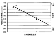
- the present inventors investigated the crystallinity of the resistance layer.
- FIG. 9 shows the growth temperature dependence of the crystallinity of the high resistance layer
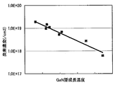
- FIG. 10 shows the growth temperature dependence of the carbon concentration of the high resistance layer.
- the present invention has been made in view of the above problems, and while reducing the leakage current by increasing the crystallinity while maintaining the high resistance of the high resistance layer, the channel layer formed thereon It is an object of the present invention to provide a semiconductor substrate and a semiconductor element which can suppress a decrease in electron mobility and occurrence of current collapse in a channel layer by increasing crystallinity.
- the present invention provides a substrate, a buffer layer made of a carbon-containing nitride-based semiconductor on the substrate, and a high resistance layer made of a carbon-containing nitride-based semiconductor on the buffer layer;
- the high resistance layer includes the first region having a carbon concentration lower than that of the buffer layer, and the second region having a carbon concentration higher than that of the first region between the first region and the channel layer.
- the crystallinity can be increased while maintaining the high resistance of the high resistance layer, thereby reducing the leakage current and increasing the crystallinity of the channel layer formed thereon. Reduction of electron mobility and current collapse in the layer can be suppressed.
- the first region includes a transition metal, and the transition metal concentration in the first region is higher than the transition metal concentration in the second region.
- the first region can suppress an increase in longitudinal leakage current in the first region having a low carbon concentration, and the first region The crystallinity of the region can be further increased, whereby the crystallinity of the nitride-based semiconductor formed above the first region can be further improved.
- the transition metal concentration in the first region is 1 ⁇ 10 17 atoms / cm 3 or more, 1 ⁇ 10 20 atoms / cm 3 or less, particularly 1 ⁇ 10 18 atoms / cm 3 or more, 1 ⁇ 10 19 atoms. / Cm 3 or less is preferable. If the transition metal concentration in the first region is such a concentration range, an increase in the longitudinal leakage current in the first region can be reliably suppressed, and the nitride formed above the first region The crystallinity of the system semiconductor can be improved reliably.
- the first region includes a transition metal, and the thickness of the first region is 3 nm or more and 3000 nm or less.
- the first region contains a transition metal and the thickness of the first region is within such a range, the first region is formed above the first region while maintaining the high resistance of the first region.
- the crystallinity of the nitride semiconductor can be improved.
- the first region does not contain a transition metal and the thickness of the first region is 3 nm or more and 500 nm or less.
- the first region is formed above the first region while maintaining suppression of the vertical leakage current.
- the crystallinity of the nitride semiconductor can be improved.
- the first region is in contact with the buffer layer.
- the carbon concentration of the first region is less than 1 ⁇ 10 18 atoms / cm 3
- the carbon concentration of the second region is 1 ⁇ 10 18 atoms / cm 3 or more, 1 ⁇ 10 19 atoms / cm 3. It is preferable that it is 3 or less.
- Such a concentration range can be suitably used as the carbon concentration in the first region and the second region.
- the present invention also provides a semiconductor device manufactured using the above semiconductor substrate, wherein an electrode is provided on the channel layer.
- a semiconductor element manufactured using such a semiconductor substrate of the present invention can increase the crystallinity while maintaining the high resistance of the high resistance layer, thereby reducing the leakage current and By increasing the crystallinity of the channel layer formed on the substrate, it is possible to suppress the decrease in electron mobility and the occurrence of current collapse in the channel layer.
- the present invention it is possible to increase the crystallinity while maintaining the high resistance of the high resistance layer, thereby reducing the leakage current and the crystallinity of the channel layer formed thereon.
- By increasing the height it is possible to suppress the decrease in electron mobility and the occurrence of current collapse in the channel layer.
- FIG. 6 is a diagram showing an impurity concentration distribution in a depth direction of a semiconductor substrate of Example 2.
- FIG. 10 is a diagram illustrating an impurity concentration distribution in a depth direction of a semiconductor substrate of Example 5.
- 6 is a cross-sectional view of a semiconductor substrate of Example 5.
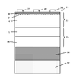
- FIG. 7 is a cross-sectional view of a semiconductor element of Example 5.
- the high resistance layer is used to suppress the vertical leakage current of the device by increasing the carbon concentration and improve the off characteristics of the transistor.
- the carbon concentration is increased, the high resistance layer Crystallinity is lowered.
- the crystallinity of the high resistance layer is lowered, the leakage current increases, and the crystallinity of the channel layer formed thereon is also lowered, thereby causing a problem of causing a decrease in electron mobility and current collapse in the channel layer. there were.
- the present inventors reduce the leakage current by increasing the crystallinity while maintaining the high resistance of the high-resistance layer, and also increase the crystallinity of the channel layer formed on the channel layer.
- the semiconductor substrate which can suppress the decrease of the electron mobility and the occurrence of current collapse in the semiconductor has been studied earnestly.
- a first region having a carbon concentration lower than that of the buffer layer, and a second region having a carbon concentration higher than that of the first region provided between the first region and the channel layer. Can increase the crystallinity while maintaining the high resistance of the high resistance layer, thereby reducing the leakage current and increasing the crystallinity of the channel layer formed thereon. It has been found that the decrease in electron mobility and the occurrence of current collapse in the channel layer can be suppressed, and the present invention has been made.
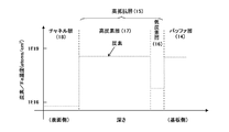
- FIG. 1 is a diagram showing a concentration distribution in the depth direction of a semiconductor substrate showing an example of an embodiment of the present invention
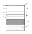
- FIG. 2 is a cross-sectional view of the semiconductor substrate of the present invention.
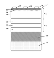
- a semiconductor substrate 10 showing an example of the embodiment of the present invention shown in FIG. 2 includes a substrate 12, a buffer layer 14 provided on the substrate 12, and a nitride-based semiconductor (for example, GaN) provided on the buffer layer 14. And a high resistance layer 15 containing transition metal and carbon as impurities, and an active layer 22 provided on the high resistance layer 15.
- the substrate 12 is a substrate made of, for example, Si or SiC.
- the buffer layer 14 is configured by, for example, a stacked body in which a first layer made of a nitride semiconductor and a second layer made of a nitride semiconductor having a composition different from that of the first layer are repeatedly stacked. It is a buffer layer.
- the first layer is made of, for example, Al y Ga 1-y N
- the second layer is made of, for example, Al x Ga 1-x N (0 ⁇ x ⁇ y ⁇ 1).
- the first layer can be AlN and the second layer can be GaN.
- the active layer 22 has a channel layer 18 made of a nitride semiconductor and a barrier layer 20 made of a nitride semiconductor provided on the channel layer 18.
- the channel layer 18 is made of, for example, GaN
- the barrier layer 20 is made of, for example, AlGaN.
- the high resistance layer 15 is provided between the low carbon layer 16 (first region) 16 in which the carbon concentration is lower than that of the buffer layer 14 and the transition metal concentration is constant, and between the low carbon layer 16 and the channel layer 18. Includes a high carbon layer (second region) 17 in which the transition metal is higher than the low carbon layer 16 and the transition metal decreases from the low carbon layer 16 side toward the channel layer 18 side.
- FIG. 1 shows a case where the high resistance layer 15 includes a transition metal, the high resistance layer 15 may not include a transition metal.
- the high resistance layer 15 includes a low carbon layer 16 having a carbon concentration lower than that of the buffer layer 14, and a high carbon layer 17 provided between the low carbon layer 16 and the channel layer 18 and having a carbon concentration higher than that of the low carbon layer 16.
- the transition metal can be Fe.
- Fe can be suitably used as the transition metal.
- Sc, Ti, V, Cr, Mn, Co, Ni, Cu, Zn, etc. can also be used as a transition metal.
- the addition of carbon is performed by incorporating carbon contained in a source gas (TMG (trimethylgallium), etc.) into the film when the nitride-based semiconductor layer is grown by the MOVPE (metal organic chemical vapor deposition) method.
- a source gas TMG (trimethylgallium), etc.
- MOVPE metal organic chemical vapor deposition
- a doping gas such as propane.
- the transition metal concentration of the low carbon layer 16 is preferably higher than the transition metal concentration of the high carbon layer 17. Since the low carbon layer 16 contains the transition metal at a higher concentration than the high carbon layer 17, it is possible to suppress an increase in the longitudinal leakage current in the low carbon layer 16 having a low carbon concentration, and the crystallinity of the low carbon layer 16. Thus, the crystallinity of the nitride semiconductor formed above the first region can be further improved.
- the transition metal concentration of the low carbon layer 16 is 1 ⁇ 10 17 atoms / cm 3 or more, 1 ⁇ 10 20 atoms / cm 3 or less, particularly 1 ⁇ 10 18 atoms / cm 3 or more, 1 ⁇ 10 19 atoms / cm 3 or less. It is preferable that If the transition metal concentration of the low carbon layer 16 is in such a concentration range, an increase in the longitudinal leakage current in the low carbon layer 16 can be reliably suppressed, and the nitride formed above the low carbon layer 16 The crystallinity of the system semiconductor can be improved reliably.
- the thickness of the low carbon layer 16 is preferably 3 nm or more and 3000 nm or less, and particularly preferably 5 nm or more and 2000 nm or less.
- the low carbon layer 16 is formed above the low carbon layer 16 while maintaining the high resistance of the low carbon layer 16. The crystallinity of the nitride semiconductor can be improved.
- the thickness of the low carbon layer 16 is preferably 3 nm or more and 500 nm or less, and particularly preferably 5 nm or more and 200 nm or less. If the low carbon layer 16 does not contain a transition metal and the thickness of the low carbon layer 16 is in such a thin range, the low carbon layer 16 is formed above the low carbon layer 16 while maintaining suppression of the vertical leakage current. The crystallinity of the nitride-based semiconductor can be improved.
- the low carbon layer 16 is preferably in contact with the buffer layer 14.
- the crystallinity of the nitride-based semiconductor formed above the low-carbon layer 16 is more effective. Can be improved.
- the carbon concentration of the low carbon layer 16 is less than 1 ⁇ 10 18 atoms / cm 3
- the carbon concentration of the second region is 1 ⁇ 10 18 atoms / cm 3 or more, and 1 ⁇ 10 19 atoms / cm 3.
- concentration range can be suitably used as the carbon concentration in the first region and the second region.
- FIG. 3 is a cross-sectional view of a semiconductor element showing an example of an embodiment of the present invention.
- the semiconductor element 11 is manufactured using the semiconductor substrate 10 of the present invention, and has a first electrode 26, a second electrode 28, and a control electrode 30 provided on the active layer 22.
- the first electrode 26 and the second electrode 28 are configured so that current flows from the first electrode 26 to the second electrode 28 through the two-dimensional electron gas layer 24 formed in the channel layer 18.
- the current flowing between the first electrode 26 and the second electrode 28 can be controlled by the potential applied to the control electrode 30.
- the semiconductor element 11 is manufactured by using the semiconductor substrate 10 showing an example of the embodiment of the present invention, and can increase the crystallinity while maintaining the high resistance of the high resistance layer, thereby leak current.
- the crystallinity of the channel layer formed thereon can be increased, so that the decrease in electron mobility and the occurrence of current collapse in the channel layer can be suppressed.
- Example 1 A semiconductor substrate as shown in FIG. 2 having a concentration distribution in the depth direction shown in FIG. 1 was produced.
- Fe is used as the transition metal
- the carbon concentration in the low carbon layer 16 is 5 ⁇ 10 17 atoms / cm 3
- the carbon concentration in the high carbon layer 17 is 2 ⁇ 10 18 atoms / cm 3
- the low carbon layer 16 The concentration of Fe in was 3 ⁇ 10 18 atoms / cm 3 .
- the thickness of the low carbon layer 16 was 500 nm
- the thickness of the high carbon layer 17 was 1600 nm.
- a semiconductor element as shown in FIG. 3 was produced using the produced semiconductor substrate.
- Example 2 A semiconductor substrate as shown in FIG. 2 having a concentration distribution in the depth direction shown in FIG. 4 was produced. However, no transition metal is added to the high resistance layer 15, the carbon concentration in the low carbon layer 16 is 3 ⁇ 10 17 atoms / cm 3, and the carbon concentration in the high carbon layer 17 is 2 ⁇ 10 18 atoms / cm 3. It was. Moreover, the thickness of the low carbon layer 16 was 100 nm, and the thickness of the high carbon layer 17 was 1600 nm. A semiconductor element as shown in FIG. 3 was produced using the produced semiconductor substrate.
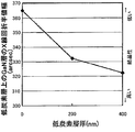
- Example 3 A semiconductor substrate was produced in the same manner as in Example 2. However, the thickness of the low carbon layer 16 was 200 nm, and the thickness of the high carbon layer 17 was 1500 nm. In the fabricated semiconductor substrate, the crystallinity of the GaN layer (including the high carbon layer 17) in the 0002 direction on the low carbon layer 16 was measured using X-ray diffraction. The result is shown in FIG. A semiconductor element as shown in FIG. 3 was produced using the produced semiconductor substrate.
- Example 4 A semiconductor substrate was produced in the same manner as in Example 2. However, the thickness of the low carbon layer 16 was 400 nm, and the thickness of the high carbon layer 17 was 1300 nm. In the fabricated semiconductor substrate, the crystallinity of the GaN layer (including the high carbon layer 17) in the 0002 direction on the low carbon layer 16 was measured using X-ray diffraction. The result is shown in FIG. A semiconductor element as shown in FIG. 3 was produced using the produced semiconductor substrate.
- Example 2 A semiconductor substrate was produced in the same manner as in Example 2. However, the low carbon layer 16 was not formed, and the thickness of the high carbon layer 17 was 1700 nm. In the fabricated semiconductor substrate, the crystallinity of the GaN layer in the 0002 direction including the high carbon layer 17 was measured using X-ray diffraction. The result is shown in FIG. A semiconductor element as shown in FIG. 3 (however, the low carbon layer 16 is not formed) was produced using the produced semiconductor substrate.
- the high resistance layer 15 further includes a high carbon layer (third region) 19 having a carbon concentration higher than that of the low carbon layer 16 between the buffer layer 14 and the low carbon layer 16. 4 is the same as that of the semiconductor substrate 10 shown in FIGS.
- the carbon concentration in the low carbon layer 16 is 3 ⁇ 10 17 atoms / cm 3
- the carbon concentration in the high carbon layer 17 is 2 ⁇ 10 18 atoms / cm 3.
- the carbon concentration in the high carbon layer 19 was 2 ⁇ 10 18 atoms / cm 3 .
- the thickness of the low carbon layer 16 was 100 nm
- the thickness of the high carbon layer 17 was 800 nm
- the thickness of the high carbon layer 19 was 800 nm.
- a transition region 21 in which the carbon concentration gradually increases may be provided between the low carbon layer 16 and the high carbon layer 17.
- a semiconductor element as shown in FIG. 7 was manufactured using the manufactured semiconductor substrate.
- the high resistance layer 15 further includes a high carbon layer (third region) 19 having a carbon concentration higher than that of the low carbon layer 16 between the buffer layer 14 and the low carbon layer 16. Except for this, the configuration is the same as that of the semiconductor element 11 of FIG.
- the film thickness of the low carbon layer 16 increases and the crystallinity of the GaN layer on the low carbon layer 16 increases. That is, as compared with the comparative example in which the low carbon layer 16 is not formed, the crystal of the GaN layer (including the high carbon layer 17) on the low carbon layer 16 of the semiconductor substrate of Example 3-4 in which the low carbon layer 16 is formed. In Example 4 where the film thickness of the low carbon layer 16 is thick, the crystallinity is higher in Example 4 than in Example 3 where the film thickness of the low carbon layer 16 is thin. Further, it was confirmed that in the semiconductor device of Example 1-5, the vertical leakage current was reduced compared to the semiconductor device of the comparative example, and the decrease in electron mobility and the occurrence of current collapse were suppressed in the channel layer. did it.
- the present invention is not limited to the above embodiment.
- the above-described embodiment is an exemplification, and the present invention has substantially the same configuration as the technical idea described in the claims of the present invention, and any device that exhibits the same function and effect is the present invention. It is included in the technical scope of the invention.
- the carbon concentration of any one of the low carbon layer 16 and the high carbon layers 17 and 19 may gradually increase from the semiconductor substrate 10, 10 ′ side toward the channel 18 side. .
Landscapes
- Junction Field-Effect Transistors (AREA)
- Chemical & Material Sciences (AREA)
- Crystallography & Structural Chemistry (AREA)
- Insulated Gate Type Field-Effect Transistor (AREA)
Abstract
Description
GaN層のうち下部の層(高抵抗層)は、縦方向及び横方向の電気抵抗を高めることで、トランジスタのオフ特性向上、縦方向リークの抑制により高耐圧化が可能となる。そのためGaN層に炭素をドープし、GaN結晶中に深い準位を形成し、n型の伝導を抑制させる。
一方、GaN層のうち上部の層は、チャネル層として機能し、キャリアをトラップさせる準位が形成されると電流コラプス(出力電流特性の再現性が劣化する現象)の要因となりうるため、炭素等の濃度を十分低下させる必要がある(特許文献1-3参照)。
また、特許文献5には、寄生容量を低減させるとともに高耐圧化させるために、GaN層にFeを添加することが開示されている。
図9-10からわかるように、成長温度を下げると高抵抗層の炭素濃度を増加させることができるが、逆に高抵抗層の結晶性が低くなっている。
第1の領域が第2の領域の遷移金属濃度より高い濃度で遷移金属を含むことで、炭素濃度の低い第1の領域において縦方向リーク電流の増加を抑制することができるとともに、第1の領域の結晶性をさらに高くすることができ、これにより第1の領域より上に形成される窒化物系半導体の結晶性をさらに改善することができる。
第1の領域の遷移金属濃度がこのような濃度範囲であれば、第1の領域における縦方向リーク電流の増加を確実に抑制することができ、第1の領域より上に形成される窒化物系半導体の結晶性を確実に改善することができる。
第1の領域が遷移金属を含む場合に、第1の領域の厚さがこのような範囲であれば、第1の領域の高抵抗を維持しながら、第1の領域より上に形成される窒化物系半導体の結晶性を改善することができる。
第1の領域が遷移金属を含まない場合に、第1の領域の厚さがこのような範囲であれば、縦方向リーク電流の抑制を維持しながら、第1の領域より上に形成される窒化物系半導体の結晶性を改善することができる。
このように結晶性の高い第1の領域をよりバッファ層側に(すなわち、より基板側に)設けることにより、第1の領域より上に形成される窒化物系半導体の結晶性をより効果的に改善することができる。
第1の領域及び第2の領域の炭素濃度として、このような濃度範囲を好適に用いることができる。
図1は本発明の実施態様の一例を示す半導体基板の深さ方向の濃度分布を示した図であり、図2は本発明の半導体基板の断面図である。
ここで、基板12は、例えば、Si又はSiCからなる基板である。また、バッファ層14は、例えば、窒化物系半導体からなる第一の層と、第一の層と組成の異なる窒化物系半導体からなる第二の層とが繰り返し積層された積層体で構成されるバッファ層である。
第一の層は例えば、AlyGa1-yNからなり、第二の層は例えば、AlxGa1-xN(0≦x<y≦1)からなる。
具体的には、第一の層はAlNとすることができ、第二の層はGaNとすることができる。
なお、図1において、高抵抗層15が遷移金属を含んでいる場合を示しているが、高抵抗層15は遷移金属を含んでいなくてもよい。
高抵抗層15が、バッファ層14よりも炭素濃度が低い低炭素層16と、低炭素層16とチャネル層18との間に設けられ低炭素層16よりも炭素濃度が高い高炭素層17とを有することで、高抵抗層15の高抵抗を維持しながら結晶性を高くすることができ、それによってリーク電流を低減させるとともに、その上に形成されるチャネル層18の結晶性も高くすることでチャネル層における電子移動度の低下や電流コラプスの発生を抑制できる。
このように、遷移金属としてFeを好適に用いることができる。なお、遷移金属としてSc、Ti、V、Cr、Mn、Co、Ni、Cu、Zn等を用いることもできる。
低炭素層16が高炭素層17より高い濃度で遷移金属を含むことで、炭素濃度の低い低炭素層16において縦方向リーク電流の増加を抑制することができるとともに、低炭素層16の結晶性をさらに高くすることができ、これにより第1の領域より上に形成される窒化物系半導体の結晶性をさらに改善することができる。
低炭素層16の遷移金属濃度がこのような濃度範囲であれば、低炭素層16における縦方向リーク電流の増加を確実に抑制することができ、低炭素層16より上に形成される窒化物系半導体の結晶性を確実に改善することができる。
低炭素層16が遷移金属を含む場合に、低炭素層16の厚さがこのような範囲であれば、低炭素層16の高抵抗を維持しながら、低炭素層16より上に形成される窒化物系半導体の結晶性を改善することができる。
低炭素層16が遷移金属を含まない場合に、低炭素層16の厚さがこのような薄い範囲であれば、縦方向リーク電流の抑制を維持しながら、低炭素層16より上に形成される窒化物系半導体の結晶性を改善することができる。
このように結晶性の高い低炭素層16をよりバッファ層14側(すなわち、より基板12側に)設けることにより、低炭素層16より上に形成される窒化物系半導体の結晶性をより効果的に改善することができる。
第1の領域及び第2の領域の炭素濃度として、このような濃度範囲を好適に用いることができる。
図3は本発明の実施態様の一例を示す半導体素子の断面図である。
半導体素子11は、本発明の半導体基板10を用いて作製されたものであり、能動層22上に設けられた第一電極26、第二電極28、制御電極30を有している。
半導体素子11において、第一電極26及び第二電極28は、第一電極26から、チャネル層18内に形成された二次元電子ガス層24を介して、第二電極28に電流が流れるように配置されている。
第一電極26と第二電極28との間に流れる電流は、制御電極30に印可される電位によってコントロールすることができる。
図1に示す深さ方向の濃度分布を有する図2に示すような半導体基板を作製した。ただし、遷移金属としてFeを用い、低炭素層16における炭素濃度は、5×10¹⁷atoms/cm3とし、高炭素層17における炭素濃度は2×1018atoms/cm3とし、低炭素層16におけるFeの濃度は、3×1018atoms/cm3とした。また、低炭素層16の厚さは500nmとし、高炭素層17の厚さは1600nmとした。
作製された半導体基板を用いて図3に示すような半導体素子を作製した。
図4に示す深さ方向の濃度分布を有する図2に示すような半導体基板を作製した。ただし、高抵抗層15には遷移金属を添加せず、低炭素層16における炭素濃度は、3×10¹⁷atoms/cm3とし、高炭素層17における炭素濃度は2×1018atoms/cm3とした。また、低炭素層16の厚さは100nmとし、高炭素層17の厚さは1600nmとした。
作製された半導体基板を用いて図3に示すような半導体素子を作製した。
実施例2と同様にして半導体基板を作製した。ただし、低炭素層16の厚さは200nmとし、高炭素層17の厚さは1500nmとした。
作製した半導体基板において、低炭素層16上の0002方向のGaN層(高炭素層17を含む)の結晶性をX線回折を用いて測定した。その結果を図8に示す。
作製された半導体基板を用いて図3に示すような半導体素子を作製した。
実施例2と同様にして半導体基板を作製した。ただし、低炭素層16の厚さは400nmとし、高炭素層17の厚さは1300nmとした。
作製した半導体基板において、低炭素層16上の0002方向のGaN層(高炭素層17を含む)の結晶性をX線回折を用いて測定した。その結果を図8に示す。
作製された半導体基板を用いて図3に示すような半導体素子を作製した。
実施例2と同様にして半導体基板を作製した。ただし、低炭素層16は形成せずに、高炭素層17の厚さは1700nmとした。
作製した半導体基板において、高炭素層17を含む0002方向のGaN層の結晶性をX線回折を用いて測定した。その結果を図8に示す。
作製された半導体基板を用いて図3に示すような半導体素子(ただし、低炭素層16は形成されていない)を作製した。
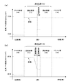
図5(a)に示す深さ方向の濃度分布を有する図6に示すような半導体基板を作製した。
図5-6に示す半導体基板10’は、高抵抗層15がさらに、炭素濃度が低炭素層16より高い高炭素層(第3の領域)19をバッファ層14と低炭素層16との間に含んでいることを除いて、図4、図2に示す半導体基板10と同様の構成となっている。ただし、高抵抗層15には遷移金属を添加せず、低炭素層16における炭素濃度は、3×10¹⁷atoms/cm3とし、高炭素層17における炭素濃度は2×1018atoms/cm3とし、高炭素層19における炭素濃度は2×1018atoms/cm3とした。また、低炭素層16の厚さは100nmとし、高炭素層17の厚さは800nmとし、高炭素層19の厚さは800nmとした。
なお、図5(b)に示すように、低炭素層16と高炭素層17との間に炭素濃度が徐々に増加する遷移領域21を設けてもよい。
作製された半導体基板を用いて図7に示すような半導体素子を作製した。
図7に示す半導体素子11’は、高抵抗層15がさらに、炭素濃度が低炭素層16より高い高炭素層(第3の領域)19をバッファ層14と低炭素層16との間に含んでいることを除いて、図3の半導体素子11と同様の構成となっている。
さらに、実施例1-5の半導体素子において、比較例の半導体素子と比較して縦方向リーク電流が減少し、チャネル層において電子移動度の低下や電流コラプスの発生が抑制されていることが確認できた。
例えば、各実施形態において、低炭素層16、高炭素層17、19の各層のいずれか1つが半導体基板10、10’側からチャネル18側に向かって炭素濃度が徐々に増加していてもよい。
Claims (9)
- 基板と、
前記基板上の炭素含有の窒化物系半導体からなるバッファ層と、
前記バッファ層上の炭素含有の窒化物系半導体からなる高抵抗層と、
前記高抵抗層上の窒化物系半導体からなるチャネル層と
を有する半導体基板であって、
前記高抵抗層は、
前記バッファ層よりも炭素濃度が低い第1の領域と、
前記第1の領域と前記チャネル層との間に設けられ、前記第1の領域よりも炭素濃度が高い第2の領域と
を有することを特徴とする半導体基板。 - 前記第1の領域が遷移金属を含み、前記第1の領域の遷移金属濃度が前記第2の領域の遷移金属濃度より高いことを特徴とする請求項1に記載の半導体基板。
- 前記第1の領域の遷移金属濃度が、1×10¹⁷atoms/cm3以上、1×1020atoms/cm3以下であることを特徴とする請求項2に記載の半導体基板。
- 前記第1の領域の遷移金属濃度が、1×10¹⁸atoms/cm3以上、1×1019atoms/cm3以下であることを特徴とする請求項3に記載の半導体基板。
- 前記第1の領域が遷移金属を含み、前記第1の領域の厚さが3nm以上、3000nm以下であることを特徴とする請求項1から請求項4のいずれか一項に記載の半導体基板。
- 前記第1の領域が遷移金属を含まず、前記第1の領域の厚さが3nm以上、500nm以下であることを特徴とする請求項1に記載の半導体基板。
- 前記第1の領域は、前記バッファ層と接していることを特徴とする請求項1から請求項6のいずれか一項に記載の半導体基板。
- 前記第1の領域の炭素濃度が1×10¹⁸atoms/cm3未満であり、前記第2の領域の炭素濃度が1×1018atoms/cm3以上、1×1019atoms/cm3以下であることを特徴とする請求項1から請求項7のいずれか一項に記載の半導体基板。
- 請求項1から請求項8のいずれか一項に記載の半導体基板を用いて作製された半導体素子であって、前記チャネル層上に電極が設けられているものであることを特徴とする半導体素子。
Priority Applications (3)
| Application Number | Priority Date | Filing Date | Title |
|---|---|---|---|
| CN201580020389.9A CN106233440B (zh) | 2014-04-18 | 2015-03-12 | 半导体基板和半导体元件 |
| US15/302,684 US9876101B2 (en) | 2014-04-18 | 2015-03-12 | Semiconductor substrate and semiconductor device |
| KR1020167028953A KR102121097B1 (ko) | 2014-04-18 | 2015-03-12 | 반도체 기판 및 반도체 소자 |
Applications Claiming Priority (2)
| Application Number | Priority Date | Filing Date | Title |
|---|---|---|---|
| JP2014086397A JP6249868B2 (ja) | 2014-04-18 | 2014-04-18 | 半導体基板及び半導体素子 |
| JP2014-086397 | 2014-04-18 |
Publications (1)
| Publication Number | Publication Date |
|---|---|
| WO2015159481A1 true WO2015159481A1 (ja) | 2015-10-22 |
Family
ID=54323709
Family Applications (1)
| Application Number | Title | Priority Date | Filing Date |
|---|---|---|---|
| PCT/JP2015/001371 Ceased WO2015159481A1 (ja) | 2014-04-18 | 2015-03-12 | 半導体基板及び半導体素子 |
Country Status (6)
| Country | Link |
|---|---|
| US (1) | US9876101B2 (ja) |
| JP (1) | JP6249868B2 (ja) |
| KR (1) | KR102121097B1 (ja) |
| CN (1) | CN106233440B (ja) |
| TW (1) | TWI596765B (ja) |
| WO (1) | WO2015159481A1 (ja) |
Families Citing this family (15)
| Publication number | Priority date | Publication date | Assignee | Title |
|---|---|---|---|---|
| JP6654957B2 (ja) * | 2015-04-23 | 2020-02-26 | ローム株式会社 | 窒化物半導体デバイス |
| CN107546260A (zh) * | 2016-06-29 | 2018-01-05 | 江西省昌大光电科技有限公司 | 一种半绝缘GaN薄膜及其制备方法 |
| JP6759886B2 (ja) * | 2016-09-06 | 2020-09-23 | 富士通株式会社 | 半導体結晶基板、半導体装置、半導体結晶基板の製造方法及び半導体装置の製造方法 |
| JP6615075B2 (ja) * | 2016-09-15 | 2019-12-04 | サンケン電気株式会社 | 半導体デバイス用基板、半導体デバイス、及び、半導体デバイス用基板の製造方法 |
| EP3486939B1 (en) | 2017-11-20 | 2020-04-01 | IMEC vzw | Method for forming a semiconductor structure for a gallium nitride channel device |
| CN113424326B (zh) * | 2019-02-01 | 2024-06-14 | 苏州晶湛半导体有限公司 | 一种半导体结构及其制备方法 |
| JP7393138B2 (ja) * | 2019-06-24 | 2023-12-06 | 住友化学株式会社 | Iii族窒化物積層体 |
| JP7269190B2 (ja) * | 2020-02-27 | 2023-05-08 | 株式会社東芝 | 窒化物結晶、光学装置、半導体装置、窒化物結晶の製造方法 |
| CN111952365A (zh) * | 2020-08-14 | 2020-11-17 | 中国科学院半导体研究所 | 碳掺杂调控的GaN基HEMT外延结构及其制作方法 |
| WO2022068256A1 (zh) * | 2020-09-30 | 2022-04-07 | 苏州能讯高能半导体有限公司 | 半导体器件的外延结构及其制备方法 |
| JP7388422B2 (ja) * | 2021-12-23 | 2023-11-29 | 信越半導体株式会社 | 窒化物半導体基板の製造方法 |
| WO2023127520A1 (ja) * | 2021-12-27 | 2023-07-06 | ローム株式会社 | 窒化物半導体装置およびその製造方法 |
| WO2023176744A1 (ja) * | 2022-03-14 | 2023-09-21 | 三菱ケミカル株式会社 | GaNエピタキシャル基板 |
| JP7682391B2 (ja) * | 2022-06-28 | 2025-05-23 | 三菱電機株式会社 | 半導体装置 |
| KR102773898B1 (ko) * | 2023-08-16 | 2025-02-27 | 웨이브로드 주식회사 | 반도체 소자 성장용 복합기판 및 그 제조 방법 |
Citations (4)
| Publication number | Priority date | Publication date | Assignee | Title |
|---|---|---|---|---|
| JP2008205146A (ja) * | 2007-02-20 | 2008-09-04 | Fujitsu Ltd | 化合物半導体装置及びその製造方法 |
| JP2011082494A (ja) * | 2009-09-14 | 2011-04-21 | Covalent Materials Corp | 化合物半導体基板 |
| JP2014049674A (ja) * | 2012-09-03 | 2014-03-17 | Hitachi Metals Ltd | 窒化物半導体ウェハ |
| JP2015053328A (ja) * | 2013-09-05 | 2015-03-19 | 富士通株式会社 | 半導体装置 |
Family Cites Families (16)
| Publication number | Priority date | Publication date | Assignee | Title |
|---|---|---|---|---|
| JP4589043B2 (ja) | 2004-07-14 | 2010-12-01 | 株式会社日立国際電気 | データ伝送装置 |
| JP4653671B2 (ja) * | 2005-03-14 | 2011-03-16 | 株式会社東芝 | 発光装置 |
| JP4792814B2 (ja) * | 2005-05-26 | 2011-10-12 | 住友電気工業株式会社 | 高電子移動度トランジスタ、電界効果トランジスタ、エピタキシャル基板、エピタキシャル基板を作製する方法およびiii族窒化物系トランジスタを作製する方法 |
| US9331192B2 (en) * | 2005-06-29 | 2016-05-03 | Cree, Inc. | Low dislocation density group III nitride layers on silicon carbide substrates and methods of making the same |
| JP5064824B2 (ja) | 2006-02-20 | 2012-10-31 | 古河電気工業株式会社 | 半導体素子 |
| JP4234180B2 (ja) * | 2007-07-02 | 2009-03-04 | 三菱電機株式会社 | 窒化物系半導体積層構造の製造方法および半導体光素子の製造方法 |
| JP4462330B2 (ja) * | 2007-11-02 | 2010-05-12 | 住友電気工業株式会社 | Iii族窒化物電子デバイス |
| JP2010123725A (ja) | 2008-11-19 | 2010-06-03 | Sanken Electric Co Ltd | 化合物半導体基板及び該化合物半導体基板を用いた半導体装置 |
| JP5696392B2 (ja) | 2010-07-29 | 2015-04-08 | 住友電気工業株式会社 | 半導体装置 |
| JP6024075B2 (ja) * | 2010-07-30 | 2016-11-09 | 住友電気工業株式会社 | 半導体装置およびその製造方法 |
| WO2012066701A1 (ja) * | 2010-11-19 | 2012-05-24 | パナソニック株式会社 | 窒化物半導体装置 |
| JP2013033930A (ja) * | 2011-06-29 | 2013-02-14 | Sumitomo Electric Ind Ltd | Iii族窒化物半導体素子、及び、iii族窒化物半導体素子の製造方法 |
| US8796738B2 (en) | 2011-09-21 | 2014-08-05 | International Rectifier Corporation | Group III-V device structure having a selectively reduced impurity concentration |
| KR101262726B1 (ko) * | 2011-12-30 | 2013-05-09 | 일진엘이디(주) | 탄소 도핑된 p형 질화물층을 포함하는 질화물계 발광소자 제조 방법 |
| JP6055918B2 (ja) * | 2013-07-19 | 2016-12-27 | シャープ株式会社 | 電界効果トランジスタ |
| JP6283250B2 (ja) * | 2014-04-09 | 2018-02-21 | サンケン電気株式会社 | 半導体基板及び半導体素子 |
-
2014
- 2014-04-18 JP JP2014086397A patent/JP6249868B2/ja active Active
-
2015
- 2015-03-12 WO PCT/JP2015/001371 patent/WO2015159481A1/ja not_active Ceased
- 2015-03-12 KR KR1020167028953A patent/KR102121097B1/ko active Active
- 2015-03-12 US US15/302,684 patent/US9876101B2/en active Active
- 2015-03-12 CN CN201580020389.9A patent/CN106233440B/zh active Active
- 2015-03-20 TW TW104109013A patent/TWI596765B/zh active
Patent Citations (4)
| Publication number | Priority date | Publication date | Assignee | Title |
|---|---|---|---|---|
| JP2008205146A (ja) * | 2007-02-20 | 2008-09-04 | Fujitsu Ltd | 化合物半導体装置及びその製造方法 |
| JP2011082494A (ja) * | 2009-09-14 | 2011-04-21 | Covalent Materials Corp | 化合物半導体基板 |
| JP2014049674A (ja) * | 2012-09-03 | 2014-03-17 | Hitachi Metals Ltd | 窒化物半導体ウェハ |
| JP2015053328A (ja) * | 2013-09-05 | 2015-03-19 | 富士通株式会社 | 半導体装置 |
Also Published As
| Publication number | Publication date |
|---|---|
| US20170033209A1 (en) | 2017-02-02 |
| US9876101B2 (en) | 2018-01-23 |
| TWI596765B (zh) | 2017-08-21 |
| CN106233440B (zh) | 2019-09-27 |
| CN106233440A (zh) | 2016-12-14 |
| JP6249868B2 (ja) | 2017-12-20 |
| JP2015207624A (ja) | 2015-11-19 |
| KR102121097B1 (ko) | 2020-06-09 |
| KR20160141756A (ko) | 2016-12-09 |
| TW201541635A (zh) | 2015-11-01 |
Similar Documents
| Publication | Publication Date | Title |
|---|---|---|
| JP6249868B2 (ja) | 半導体基板及び半導体素子 | |
| TWI614895B (zh) | 半導體基板及半導體元件 | |
| KR102174546B1 (ko) | 반도체 디바이스 및 반도체 디바이스를 설계하는 방법 | |
| JP6539128B2 (ja) | 半導体デバイス用基板、半導体デバイス、並びに半導体デバイスの製造方法 | |
| JP6615075B2 (ja) | 半導体デバイス用基板、半導体デバイス、及び、半導体デバイス用基板の製造方法 | |
| US9793363B1 (en) | GaN semiconductor device comprising carbon and iron | |
| US10181400B2 (en) | III-Nitride transistor with enhanced doping in base layer | |
| US20160211357A1 (en) | Semiconductor device | |
| KR20130092548A (ko) | 반도체 기판, 절연 게이트형 전계 효과 트랜지스터 및 반도체 기판의 제조 방법 | |
| JP2019096720A (ja) | 半導体装置、電源回路、及び、コンピュータ | |
| JP2021166232A (ja) | 半導体装置 | |
| JP6197344B2 (ja) | 半導体装置 | |
| JP2016134563A (ja) | 半導体装置 | |
| JP6261437B2 (ja) | 半導体基板の製造方法、及び半導体素子の製造方法 | |
| JP2013243196A (ja) | ダイオードの設計方法、ダイオード、及び、ダイオードの製造方法 |
Legal Events
| Date | Code | Title | Description |
|---|---|---|---|
| 121 | Ep: the epo has been informed by wipo that ep was designated in this application |
Ref document number: 15780149 Country of ref document: EP Kind code of ref document: A1 |
|
| WWE | Wipo information: entry into national phase |
Ref document number: 15302684 Country of ref document: US |
|
| ENP | Entry into the national phase |
Ref document number: 20167028953 Country of ref document: KR Kind code of ref document: A |
|
| NENP | Non-entry into the national phase |
Ref country code: DE |
|
| 122 | Ep: pct application non-entry in european phase |
Ref document number: 15780149 Country of ref document: EP Kind code of ref document: A1 |