WO2015137420A1 - 炭化珪素半導体装置の製造方法および炭化珪素半導体装置 - Google Patents
炭化珪素半導体装置の製造方法および炭化珪素半導体装置 Download PDFInfo
- Publication number
- WO2015137420A1 WO2015137420A1 PCT/JP2015/057218 JP2015057218W WO2015137420A1 WO 2015137420 A1 WO2015137420 A1 WO 2015137420A1 JP 2015057218 W JP2015057218 W JP 2015057218W WO 2015137420 A1 WO2015137420 A1 WO 2015137420A1
- Authority
- WO
- WIPO (PCT)
- Prior art keywords
- silicon carbide
- semiconductor device
- region
- carbide semiconductor
- film
- Prior art date
- Legal status (The legal status is an assumption and is not a legal conclusion. Google has not performed a legal analysis and makes no representation as to the accuracy of the status listed.)
- Ceased
Links
Images


Classifications
-
- H—ELECTRICITY
- H10—SEMICONDUCTOR DEVICES; ELECTRIC SOLID-STATE DEVICES NOT OTHERWISE PROVIDED FOR
- H10D—INORGANIC ELECTRIC SEMICONDUCTOR DEVICES
- H10D62/00—Semiconductor bodies, or regions thereof, of devices having potential barriers
- H10D62/80—Semiconductor bodies, or regions thereof, of devices having potential barriers characterised by the materials
- H10D62/83—Semiconductor bodies, or regions thereof, of devices having potential barriers characterised by the materials being Group IV materials, e.g. B-doped Si or undoped Ge
- H10D62/832—Semiconductor bodies, or regions thereof, of devices having potential barriers characterised by the materials being Group IV materials, e.g. B-doped Si or undoped Ge being Group IV materials comprising two or more elements, e.g. SiGe
- H10D62/8325—Silicon carbide
-
- H—ELECTRICITY
- H10—SEMICONDUCTOR DEVICES; ELECTRIC SOLID-STATE DEVICES NOT OTHERWISE PROVIDED FOR
- H10W—GENERIC PACKAGES, INTERCONNECTIONS, CONNECTORS OR OTHER CONSTRUCTIONAL DETAILS OF DEVICES COVERED BY CLASS H10
- H10W20/00—Interconnections in chips, wafers or substrates
- H10W20/01—Manufacture or treatment
- H10W20/031—Manufacture or treatment of conductive parts of the interconnections
- H10W20/056—Manufacture or treatment of conductive parts of the interconnections by filling conductive material into holes, grooves or trenches
-
- H—ELECTRICITY
- H10—SEMICONDUCTOR DEVICES; ELECTRIC SOLID-STATE DEVICES NOT OTHERWISE PROVIDED FOR
- H10D—INORGANIC ELECTRIC SEMICONDUCTOR DEVICES
- H10D12/00—Bipolar devices controlled by the field effect, e.g. insulated-gate bipolar transistors [IGBT]
- H10D12/01—Manufacture or treatment
- H10D12/031—Manufacture or treatment of IGBTs
-
- H—ELECTRICITY
- H10—SEMICONDUCTOR DEVICES; ELECTRIC SOLID-STATE DEVICES NOT OTHERWISE PROVIDED FOR
- H10D—INORGANIC ELECTRIC SEMICONDUCTOR DEVICES
- H10D30/00—Field-effect transistors [FET]
- H10D30/60—Insulated-gate field-effect transistors [IGFET]
-
- H—ELECTRICITY
- H10—SEMICONDUCTOR DEVICES; ELECTRIC SOLID-STATE DEVICES NOT OTHERWISE PROVIDED FOR
- H10D—INORGANIC ELECTRIC SEMICONDUCTOR DEVICES
- H10D30/00—Field-effect transistors [FET]
- H10D30/60—Insulated-gate field-effect transistors [IGFET]
- H10D30/64—Double-diffused metal-oxide semiconductor [DMOS] FETs
- H10D30/66—Vertical DMOS [VDMOS] FETs
-
- H—ELECTRICITY
- H10—SEMICONDUCTOR DEVICES; ELECTRIC SOLID-STATE DEVICES NOT OTHERWISE PROVIDED FOR
- H10D—INORGANIC ELECTRIC SEMICONDUCTOR DEVICES
- H10D62/00—Semiconductor bodies, or regions thereof, of devices having potential barriers
- H10D62/10—Shapes, relative sizes or dispositions of the regions of the semiconductor bodies; Shapes of the semiconductor bodies
- H10D62/17—Semiconductor regions connected to electrodes not carrying current to be rectified, amplified or switched, e.g. channel regions
- H10D62/393—Body regions of DMOS transistors or IGBTs
-
- H—ELECTRICITY
- H10—SEMICONDUCTOR DEVICES; ELECTRIC SOLID-STATE DEVICES NOT OTHERWISE PROVIDED FOR
- H10D—INORGANIC ELECTRIC SEMICONDUCTOR DEVICES
- H10D62/00—Semiconductor bodies, or regions thereof, of devices having potential barriers
- H10D62/80—Semiconductor bodies, or regions thereof, of devices having potential barriers characterised by the materials
- H10D62/81—Semiconductor bodies, or regions thereof, of devices having potential barriers characterised by the materials of structures exhibiting quantum-confinement effects, e.g. single quantum wells; of structures having periodic or quasi-periodic potential variation
-
- H—ELECTRICITY
- H10—SEMICONDUCTOR DEVICES; ELECTRIC SOLID-STATE DEVICES NOT OTHERWISE PROVIDED FOR
- H10D—INORGANIC ELECTRIC SEMICONDUCTOR DEVICES
- H10D64/00—Electrodes of devices having potential barriers
- H10D64/01—Manufacture or treatment
- H10D64/011—Manufacture or treatment of electrodes ohmically coupled to a semiconductor
-
- H—ELECTRICITY
- H10—SEMICONDUCTOR DEVICES; ELECTRIC SOLID-STATE DEVICES NOT OTHERWISE PROVIDED FOR
- H10D—INORGANIC ELECTRIC SEMICONDUCTOR DEVICES
- H10D64/00—Electrodes of devices having potential barriers
- H10D64/01—Manufacture or treatment
- H10D64/013—Manufacture or treatment of electrodes having a conductor capacitively coupled to a semiconductor by an insulator
- H10D64/01366—Manufacture or treatment of electrodes having a conductor capacitively coupled to a semiconductor by an insulator the semiconductor being silicon carbide
-
- H—ELECTRICITY
- H10—SEMICONDUCTOR DEVICES; ELECTRIC SOLID-STATE DEVICES NOT OTHERWISE PROVIDED FOR
- H10D—INORGANIC ELECTRIC SEMICONDUCTOR DEVICES
- H10D64/00—Electrodes of devices having potential barriers
- H10D64/20—Electrodes characterised by their shapes, relative sizes or dispositions
- H10D64/23—Electrodes carrying the current to be rectified, amplified, oscillated or switched, e.g. sources, drains, anodes or cathodes
-
- H—ELECTRICITY
- H10—SEMICONDUCTOR DEVICES; ELECTRIC SOLID-STATE DEVICES NOT OTHERWISE PROVIDED FOR
- H10D—INORGANIC ELECTRIC SEMICONDUCTOR DEVICES
- H10D64/00—Electrodes of devices having potential barriers
- H10D64/60—Electrodes characterised by their materials
- H10D64/62—Electrodes ohmically coupled to a semiconductor
-
- H—ELECTRICITY
- H10—SEMICONDUCTOR DEVICES; ELECTRIC SOLID-STATE DEVICES NOT OTHERWISE PROVIDED FOR
- H10W—GENERIC PACKAGES, INTERCONNECTIONS, CONNECTORS OR OTHER CONSTRUCTIONAL DETAILS OF DEVICES COVERED BY CLASS H10
- H10W20/00—Interconnections in chips, wafers or substrates
- H10W20/01—Manufacture or treatment
- H10W20/031—Manufacture or treatment of conductive parts of the interconnections
- H10W20/032—Manufacture or treatment of conductive parts of the interconnections of conductive barrier, adhesion or liner layers
- H10W20/033—Manufacture or treatment of conductive parts of the interconnections of conductive barrier, adhesion or liner layers in openings in dielectrics
- H10W20/035—Manufacture or treatment of conductive parts of the interconnections of conductive barrier, adhesion or liner layers in openings in dielectrics combinations of barrier, adhesion or liner layers, e.g. multi-layered barrier layers
-
- H—ELECTRICITY
- H10—SEMICONDUCTOR DEVICES; ELECTRIC SOLID-STATE DEVICES NOT OTHERWISE PROVIDED FOR
- H10W—GENERIC PACKAGES, INTERCONNECTIONS, CONNECTORS OR OTHER CONSTRUCTIONAL DETAILS OF DEVICES COVERED BY CLASS H10
- H10W20/00—Interconnections in chips, wafers or substrates
- H10W20/40—Interconnections external to wafers or substrates, e.g. back-end-of-line [BEOL] metallisations or vias connecting to gate electrodes
- H10W20/41—Interconnections external to wafers or substrates, e.g. back-end-of-line [BEOL] metallisations or vias connecting to gate electrodes characterised by their conductive parts
- H10W20/425—Barrier, adhesion or liner layers
-
- H—ELECTRICITY
- H10—SEMICONDUCTOR DEVICES; ELECTRIC SOLID-STATE DEVICES NOT OTHERWISE PROVIDED FOR
- H10D—INORGANIC ELECTRIC SEMICONDUCTOR DEVICES
- H10D64/00—Electrodes of devices having potential barriers
- H10D64/01—Manufacture or treatment
- H10D64/011—Manufacture or treatment of electrodes ohmically coupled to a semiconductor
- H10D64/0111—Manufacture or treatment of electrodes ohmically coupled to a semiconductor to Group IV semiconductors
- H10D64/0115—Manufacture or treatment of electrodes ohmically coupled to a semiconductor to Group IV semiconductors to silicon carbide
Definitions
- the present invention relates to a method for manufacturing a silicon carbide semiconductor device using a silicon carbide substrate and a silicon carbide semiconductor device.
- SiC silicon carbide
- SiC semiconductor devices can reduce the resistance of elements in the on state to hundreds of times, and can be used in higher temperature (200 ° C or higher) environments.
- This is due to the characteristics of the material itself that the band gap of SiC is about three times as large as that of Si, and that the breakdown field strength is nearly an order of magnitude greater than that of Si.
- SiC MOSFET Metal Oxide Semiconductor Field Effect Transistor
- SiC MOSFETs with low element resistance have been proposed in which channel mobility is greatly improved by improving the annealing method after oxidation and called POA (Post Oxidation Anneal).
- the threshold voltage which was +3 V before the voltage application, was reduced to -12 V after applying a voltage of ⁇ 20 V for 10 minutes at 200 ° C.
- the interface states are mainly SiC dangling bonds (unbonded hands), but in order to reduce the interface states, annealing is performed in an atmosphere of nitrogen-containing NO gas or N 2 O gas after gate oxidation. However, it has become the mainstream for gate oxide film formation in recent SiC MOSFETs.
- N (3-coordinate) structure nitrogen is present in the vicinity, when it has active hydrogen and holes (holes), it becomes positively charged according to the reaction formula shown in the following formula (1-1). .
- the SiCn type MOSFET has a problem that the threshold voltage is lowered when a negative voltage is continuously applied to the gate of the MOSFET at a high temperature.
- the present invention provides a method for manufacturing a silicon carbide semiconductor device and a silicon carbide semiconductor device capable of suppressing a decrease in threshold voltage even when a negative voltage is applied to a gate at a high temperature in order to solve the above-described problems caused by the prior art. For the purpose.
- a method for manufacturing a silicon carbide semiconductor device of the present invention includes a step of forming a low-concentration first conductivity type silicon carbide layer on the front surface side of a first conductivity type silicon carbide substrate, and Selectively forming a second conductivity type region in the surface layer of the silicon carbide layer; selectively forming a first conductivity type source region in the region; and electrically connecting the source region to the source region Forming a source electrode connected to the gate, forming a gate insulating film on a surface of the region sandwiched between the silicon carbide layer and the source region, and forming a gate on the gate insulating film
- the metal wiring for the semiconductor device connected to the source electrode is made of aluminum.
- the shape as material A step of, characterized in that it comprises a a step of cold nitrogen annealing after the metal wiring formation.
- a titanium film is formed between the metal wiring and the silicon carbide semiconductor substrate.
- a titanium nitride film is formed between the titanium film and the silicon carbide semiconductor substrate.
- a titanium film and a titanium nitride film are formed between the titanium film and the silicon carbide semiconductor substrate.
- a silicon carbide semiconductor device of the present invention includes a first conductivity type silicon carbide substrate, a low concentration first conductivity type silicon carbide layer formed on a front surface side of the silicon carbide substrate, and the silicon carbide layer.
- a second conductive type region selectively formed in the surface layer of the first conductive type, a first conductive type source region selectively generated in the region, and electrically connected to the source region
- a source electrode a gate insulating film formed on a surface of the region sandwiched between the silicon carbide layer and the source region, a gate electrode formed on the gate insulating film, and the silicon carbide
- the metal wiring for the semiconductor device is formed by using aluminum connected to the source electrode as a material, and after the formation by low-temperature nitrogen annealing And have And wherein the Rukoto.
- the hydrogen concentration of the metal wiring is 2 ⁇ 10 11 cm ⁇ 2 or more and 2 ⁇ 10 12 cm ⁇ 2 or less.
- the low temperature nitrogen annealing is performed after forming the metal wiring for the semiconductor device. Thereby, the hydrogen concentration in the aluminum used for the metal wiring can be lowered, and the reduction of the threshold voltage is suppressed.
- the threshold voltage can be prevented from decreasing.
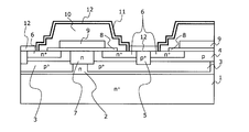
- FIG. 1 is a cross-sectional view showing a configuration of the silicon carbide semiconductor device according to the embodiment.
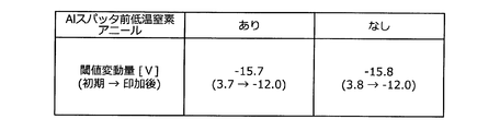
- FIG. 2 is a chart showing threshold fluctuation amounts depending on the presence or absence of low-temperature nitrogen annealing before aluminum sputtering.
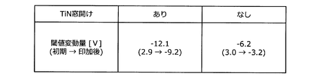
- FIG. 3 is a chart showing threshold fluctuation amounts depending on the presence / absence of opening of the TiN film.
- FIG. 4 is a chart showing threshold fluctuation amounts due to differences in film structures.
- FIG. 5 is a cross sectional view showing a state after metal wiring of the silicon carbide semiconductor device according to Working Example 1 of the invention.
- FIG. 6 is a cross sectional view showing a state after metal wiring of the silicon carbide semiconductor device according to Working Example 2 of the invention.
- FIG. 1 is a cross-sectional view showing a configuration of the silicon carbide semiconductor device according to the embodiment.
- FIG. 1 shows the state of the active region before the metal wiring is sputtered in the manufacturing process of the n-type MOSFET.
- N + type silicon carbide substrate 1, n type silicon carbide epitaxial layer 2 and p type silicon carbide epitaxial layer 4 are combined to form a silicon carbide semiconductor substrate.
- n-type silicon carbide epitaxial layer (silicon carbide layer) 2 is deposited on the main surface of n + -type silicon carbide substrate 1 of the first conductivity type serving as a drain region.
- a back electrode (not shown) is provided on the surface opposite to the n-type silicon carbide epitaxial layer 2 side of n + -type silicon carbide substrate 1 (the back surface of the silicon carbide semiconductor substrate). The back electrode constitutes a drain electrode.
- a MOS (insulating gate made of metal-oxide film-semiconductor) structure (element structure portion) is formed on the front surface side of the silicon carbide semiconductor substrate.
- the surface layer opposite to the n + -type silicon carbide substrate 1 side of the n-type silicon carbide epitaxial layer 2 (on the front surface side of the silicon carbide semiconductor substrate) has a second layer.
- a conductive p + -type region (hereinafter referred to as a p + -type base region) 3 is selectively provided.
- a p-type silicon carbide epitaxial layer 4 is selectively deposited on the surface of p + -type base region 3 and the surface of n-type silicon carbide epitaxial layer 2 between the adjacent p + -type base regions 3. Has been.
- n + type source region 6 and a p + type contact region 5 are provided on a portion of p type silicon carbide epitaxial layer 4 on p + type base region 3.
- the n + type source region 6 and the p + type contact region 5 are in contact with each other. Further, p + type contact region 5 penetrates p type silicon carbide epitaxial layer 4 in the depth direction and reaches p + type base region 3.
- n-type well region 7 that penetrates p-type silicon carbide epitaxial layer 4 in the depth direction and reaches n-type silicon carbide epitaxial layer 2 is formed. Is provided. N type well region 7 functions as a drift region together with n type silicon carbide epitaxial layer 2.
- a gate electrode 9 is provided via a gate insulating film 8.
- the gate electrode 9 may be provided on the surface of the n-type well region 7 via the gate insulating film 8.
- Interlayer insulating film 10 is provided on the entire front surface side of the silicon carbide semiconductor substrate so as to cover gate electrode 9.
- a TiN (titanium nitride) film 11 is formed on the polysilicon constituting the gate electrode 9 and the interlayer insulating film 10.
- Ni (nickel) film 12 is provided on the n + type source region 6 and the p + type contact region 5 exposed in the contact holes. Ni film 12 forms an ohmic junction with the silicon carbide semiconductor substrate and functions as a source electrode. The source electrode is electrically insulated from the gate electrode 9 by the interlayer insulating film 10.
- a metal is formed by sputtering on the Ni film 12 of the insulated gate field effect transistor (MOSFET) having the structure shown in FIG. Form wiring.
- MOSFET insulated gate field effect transistor
- this metal wiring is formed by depositing an Al (aluminum) electrode 13 (see FIG. 5) or sequentially depositing a Ti (titanium) film 14 and an Al electrode 13 (see FIG. 6).
- low temperature nitrogen annealing at about 320 ° C. to 420 ° C. is performed.
- the inventors can reduce the hydrogen concentration in aluminum used for the metal wiring to 2 ⁇ 10 11 cm ⁇ 2 or more and 2 ⁇ 10 12 cm ⁇ 2 or less by this low-temperature nitrogen annealing, thereby reducing the threshold voltage. It was found that it can be suppressed.
- Low-temperature nitrogen annealing is somewhat effective even after deposition of the final protective film (not shown) formed on the outermost surface on the metal wiring, but active hydrogen in aluminum diffuses out of the SiC MOSFET by the final protective film. Therefore, it is desirable to carry out after the metal wiring is formed and before the final protective film is deposited.
- the inventors have found from the experimental facts (1) to (3) below that the active hydrogen originates from aluminum as the metal wiring, and the higher the temperature, the faster the hydrogen diffuses. It was considered that the active hydrogen that reached the gate oxide film / SiC interface caused a reaction of the above formula (1-1) with holes accumulated at a high density with a gate negative bias, thereby causing a decrease in threshold voltage. As an improvement measure, low temperature nitrogen annealing was applied to diffuse out active hydrogen.
- FIG. 2 is a chart showing threshold fluctuation amounts depending on the presence or absence of low-temperature nitrogen annealing before aluminum sputtering. The amount of change in the threshold before and after applying a negative voltage to the gate of the MOSFET at a high temperature is shown.
- FIG. 3 is a chart showing threshold fluctuation amounts depending on the presence / absence of opening of the TiN film.
- FIG. 4 is a chart showing the threshold fluctuation amount due to the difference in the film structure. Furthermore, the inventors have also found that the threshold reduction is further improved as shown in FIG. 4 by inserting a titanium (Ti) film under the aluminum (Al) electrode.
- the Ti film is known as a hydrogen storage alloy and is considered to be a result of efficiently storing hydrogen from aluminum (Al).
- FIG. 5 is a cross sectional view showing a state after metal wiring of the silicon carbide semiconductor device according to Working Example 1 of the invention.
- FIG. 5 is a cross-sectional view after sputtering the aluminum (Al) 13 as the metal wiring after the state shown in FIG. 1 and processing it into a desired wiring shape by photolithography.
- Example 1 the aluminum 13 is etched with the same resist pattern.
- low temperature nitrogen annealing is performed at a temperature of about 320 to 420 ° C. for about 1 to 2 hours.
- the active hydrogen entering the inside of the aluminum 13 diffuses outward, and the hydrogen concentration inside the aluminum 13 is reduced.
- the degree of threshold reduction can be reduced.
- Low-temperature nitrogen annealing can be effective even after deposition of the final protective film formed on the metal wiring (aluminum 13), but active hydrogen in the aluminum 13 is less likely to diffuse out of the SiC MOSFET by the final protective film. Therefore, it is desirable that the metal wiring is formed after the aluminum 13 and before the final protective film is deposited.
- FIG. 6 is a cross sectional view showing a state after metal wiring of the silicon carbide semiconductor device according to Working Example 2 of the invention. A case where a titanium (Ti) film 14 is formed immediately below the aluminum 13 is shown. After the state shown in FIG. 1, a titanium (Ti) film 14 and aluminum (Al) 13 of metal wiring are sequentially sputtered and processed into a desired wiring shape by photolithography.
- the titanium film 14 occludes active hydrogen, so the n + type silicon carbide substrate 1. It is possible to eliminate almost all of the active hydrogen that reaches By inserting a titanium (Ti) film 14 between the TiN film 11 and the aluminum (Al) 13 as shown in FIG. 4 (center column, right column), the threshold value can be further improved.
- the low-temperature nitrogen annealing is performed after the metal wiring of the MOSFET is formed.
- This low-temperature nitrogen annealing is performed at about 320 to 420 ° C., for example.
- active hydrogen in aluminum used for the metal wiring can be diffused out.
- the hydrogen concentration of the metal wiring can be 2 ⁇ 10 11 cm ⁇ 2 or more and 2 ⁇ 10 12 cm ⁇ 2 or less.
- the p + -type contact region 5 and the n + -type source region 6 may be formed in the p + -type base region 3 without forming the p-type silicon carbide epitaxial layer 4. Good.
- the method for manufacturing a silicon carbide semiconductor device and the silicon carbide semiconductor device according to the present invention are useful for a high voltage silicon carbide semiconductor device used for power supply devices such as power conversion devices and various industrial machines. is there.
Landscapes
- Electrodes Of Semiconductors (AREA)
Abstract
Description
図5は、本発明の実施例1にかかる炭化珪素半導体装置の金属配線後の状態を示す断面図である。図5は、図1に示した状態の後に、金属配線としてのアルミニウム(Al)13をスパッタし、そしてフォトリソグラフによるエッチングで所望の配線形状に加工した後の断面図である。
図6は、本発明の実施例2にかかる炭化珪素半導体装置の金属配線後の状態を示す断面図である。アルミニウム13の直下にチタン(Ti)膜14を形成した場合を示す。図1に示した状態の後に、金属配線のチタン(Ti)膜14とアルミニウム(Al)13を順次スパッタし、そしてフォトリソグラフで所望の配線形状に加工する。
2 n型炭化珪素エピタキシャル層
3 p+型ベース領域
4 p型炭化珪素エピタキシャル層
5 p+型コンタクト領域
6 n+型ソース領域
7 n型ウェル領域
8 ゲート絶縁膜
9 ゲート電極
10 層間絶縁膜
11 窒化チタン膜
12 ニッケル膜
13 金属配線(アルミニウム)
14 チタン膜
Claims (6)
- 第1導電型の炭化珪素基板のおもて面側に低濃度の第1導電型の炭化珪素層を形成する工程と、前記炭化珪素層の表面層に第2導電型の領域を選択的に形成する工程と、前記領域内に第1導電型のソース領域を選択的に形成する工程と、前記ソース領域に電気的に接続されたソース電極を形成する工程と、前記領域の、前記炭化珪素層と前記ソース領域とに挟まれた部分の表面上にゲート絶縁膜を形成する工程と、前記ゲート絶縁膜上にゲート電極を形成する工程と、前記炭化珪素基板の裏面側にドレイン電極を形成する工程と、を有する炭化珪素半導体装置の製造方法において、
前記ソース電極に接続された半導体装置用の金属配線を、アルミニウムを材料として形成する工程と、
前記金属配線形成後に低温窒素アニールする工程と、
を含むことを特徴とする炭化珪素半導体装置の製造方法。 - 前記金属配線と炭化珪素半導体基板との間にチタン膜が形成されたことを特徴とする請求項1に記載の炭化珪素半導体装置の製造方法。
- 前記チタン膜と炭化珪素半導体基板との間に窒化チタン膜が形成されたことを特徴とする請求項2に記載の炭化珪素半導体装置の製造方法。
- 前記チタン膜と炭化珪素半導体基板との間にチタン膜および窒化チタン膜が形成されたことを特徴とする請求項2または3に記載の炭化珪素半導体装置の製造方法。
- 第1導電型の炭化珪素基板と、前記炭化珪素基板のおもて面側に形成された低濃度の第1導電型の炭化珪素層と、前記炭化珪素層の表面層に選択的に形成された第2導電型の領域と、前記領域内に選択的に生成された第1導電型のソース領域と、前記ソース領域に電気的に接続して形成されたソース電極と、前記領域の、前記炭化珪素層と前記ソース領域とに挟まれた部分の表面上に形成されたゲート絶縁膜と、前記ゲート絶縁膜上に形成されたゲート電極と、前記炭化珪素基板の裏面側に形成されたドレイン電極と、を有する炭化珪素半導体装置において、
前記ソース電極に接続されたアルミニウムを材料として形成し、当該形成後に低温窒素アニールにより形成される半導体装置用の金属配線と、
を有することを特徴とする炭化珪素半導体装置。 - 前記金属配線の水素濃度が2×1011cm-2以上2×1012cm-2以下であることを特徴とする請求項5に記載の炭化珪素半導体装置。
Priority Applications (4)
| Application Number | Priority Date | Filing Date | Title |
|---|---|---|---|
| CN201580006779.0A CN105940498B (zh) | 2014-03-11 | 2015-03-11 | 碳化硅半导体装置的制造方法及碳化硅半导体装置 |
| DE112015000352.5T DE112015000352B4 (de) | 2014-03-11 | 2015-03-11 | Verfahren zum Herstellen einer Siliciumcarbid-Halbleitervorrichtung und Siliciumcarbid-Halbleitervorrichtung |
| JP2016507806A JP6192190B2 (ja) | 2014-03-11 | 2015-03-11 | 炭化珪素半導体装置の製造方法および炭化珪素半導体装置 |
| US15/221,678 US10103059B2 (en) | 2014-03-11 | 2016-07-28 | Method of manufacturing silicon carbide semiconductor device and silicon carbide semiconductor device |
Applications Claiming Priority (2)
| Application Number | Priority Date | Filing Date | Title |
|---|---|---|---|
| JP2014-048227 | 2014-03-11 | ||
| JP2014048227 | 2014-03-11 |
Related Child Applications (1)
| Application Number | Title | Priority Date | Filing Date |
|---|---|---|---|
| US15/221,678 Continuation US10103059B2 (en) | 2014-03-11 | 2016-07-28 | Method of manufacturing silicon carbide semiconductor device and silicon carbide semiconductor device |
Publications (1)
| Publication Number | Publication Date |
|---|---|
| WO2015137420A1 true WO2015137420A1 (ja) | 2015-09-17 |
Family
ID=54071859
Family Applications (1)
| Application Number | Title | Priority Date | Filing Date |
|---|---|---|---|
| PCT/JP2015/057218 Ceased WO2015137420A1 (ja) | 2014-03-11 | 2015-03-11 | 炭化珪素半導体装置の製造方法および炭化珪素半導体装置 |
Country Status (5)
| Country | Link |
|---|---|
| US (1) | US10103059B2 (ja) |
| JP (1) | JP6192190B2 (ja) |
| CN (1) | CN105940498B (ja) |
| DE (1) | DE112015000352B4 (ja) |
| WO (1) | WO2015137420A1 (ja) |
Cited By (5)
| Publication number | Priority date | Publication date | Assignee | Title |
|---|---|---|---|---|
| JP2017108074A (ja) * | 2015-12-11 | 2017-06-15 | 富士電機株式会社 | 半導体装置および半導体装置の製造方法 |
| JP2017168687A (ja) * | 2016-03-16 | 2017-09-21 | 富士電機株式会社 | 炭化珪素半導体装置および炭化珪素半導体装置の製造方法 |
| JP2017168673A (ja) * | 2016-03-16 | 2017-09-21 | 富士電機株式会社 | 炭化珪素半導体素子および炭化珪素半導体素子の製造方法 |
| JP2017168680A (ja) * | 2016-03-16 | 2017-09-21 | 富士電機株式会社 | 炭化珪素半導体装置および炭化珪素半導体装置の製造方法 |
| JP2017168602A (ja) * | 2016-03-15 | 2017-09-21 | 富士電機株式会社 | 半導体装置および半導体装置の製造方法 |
Families Citing this family (5)
| Publication number | Priority date | Publication date | Assignee | Title |
|---|---|---|---|---|
| KR101896332B1 (ko) * | 2016-12-13 | 2018-09-07 | 현대자동차 주식회사 | 반도체 소자 및 그 제조 방법 |
| JP2018182032A (ja) * | 2017-04-11 | 2018-11-15 | 富士電機株式会社 | 炭化珪素半導体装置および炭化珪素半導体装置の製造方法 |
| JP7013735B2 (ja) * | 2017-09-05 | 2022-02-01 | 富士電機株式会社 | 炭化珪素半導体装置および炭化珪素半導体装置の製造方法 |
| JP6863464B2 (ja) * | 2017-09-05 | 2021-04-21 | 富士電機株式会社 | 炭化珪素半導体装置および炭化珪素半導体装置の製造方法 |
| JP7098927B2 (ja) * | 2017-12-25 | 2022-07-12 | 富士電機株式会社 | 炭化珪素mosfetインバータ回路 |
Citations (3)
| Publication number | Priority date | Publication date | Assignee | Title |
|---|---|---|---|---|
| JP2005327799A (ja) * | 2004-05-12 | 2005-11-24 | Sanyo Electric Co Ltd | 半導体装置の製造方法 |
| WO2014024568A1 (ja) * | 2012-08-07 | 2014-02-13 | 住友電気工業株式会社 | 炭化珪素半導体装置およびその製造方法 |
| WO2014027520A1 (ja) * | 2012-08-13 | 2014-02-20 | 住友電気工業株式会社 | 炭化珪素半導体装置 |
Family Cites Families (8)
| Publication number | Priority date | Publication date | Assignee | Title |
|---|---|---|---|---|
| JPS63308347A (ja) * | 1987-06-10 | 1988-12-15 | Nec Corp | Mos型半導体装置 |
| KR930703707A (ko) | 1991-01-30 | 1993-11-30 | 죤 죠셉 우르수 | 폴리실리콘 박막 트랜지스터 |
| JP2010502031A (ja) * | 2006-09-01 | 2010-01-21 | エヌエックスピー ビー ヴィ | 炭化ケイ素mosfetの反転層移動度を改善する方法 |
| JP5098294B2 (ja) * | 2006-10-30 | 2012-12-12 | 株式会社デンソー | 炭化珪素半導体装置の製造方法 |
| JP2011082454A (ja) | 2009-10-09 | 2011-04-21 | Panasonic Corp | 絶縁膜構造体及びこれを用いた半導体装置 |
| JP2011134910A (ja) * | 2009-12-24 | 2011-07-07 | Rohm Co Ltd | SiC電界効果トランジスタ |
| JP5685020B2 (ja) | 2010-07-23 | 2015-03-18 | 住友電気工業株式会社 | 半導体装置の製造方法 |
| JP2013247141A (ja) * | 2012-05-23 | 2013-12-09 | Mitsubishi Electric Corp | 炭化珪素半導体装置の製造方法 |
-
2015
- 2015-03-11 WO PCT/JP2015/057218 patent/WO2015137420A1/ja not_active Ceased
- 2015-03-11 CN CN201580006779.0A patent/CN105940498B/zh active Active
- 2015-03-11 JP JP2016507806A patent/JP6192190B2/ja active Active
- 2015-03-11 DE DE112015000352.5T patent/DE112015000352B4/de active Active
-
2016
- 2016-07-28 US US15/221,678 patent/US10103059B2/en active Active
Patent Citations (3)
| Publication number | Priority date | Publication date | Assignee | Title |
|---|---|---|---|---|
| JP2005327799A (ja) * | 2004-05-12 | 2005-11-24 | Sanyo Electric Co Ltd | 半導体装置の製造方法 |
| WO2014024568A1 (ja) * | 2012-08-07 | 2014-02-13 | 住友電気工業株式会社 | 炭化珪素半導体装置およびその製造方法 |
| WO2014027520A1 (ja) * | 2012-08-13 | 2014-02-20 | 住友電気工業株式会社 | 炭化珪素半導体装置 |
Non-Patent Citations (1)
| Title |
|---|
| ATTHAWUT CHANTHAPHAN ET AL.: "Understanding and controlling bias-temperature instability in SiC metal-oxide- semiconductor devices induced by unusual generation of mobile ions", APPLIED PHYSICS LETTERS, pages 093510, XP012170359 * |
Cited By (7)
| Publication number | Priority date | Publication date | Assignee | Title |
|---|---|---|---|---|
| JP2017108074A (ja) * | 2015-12-11 | 2017-06-15 | 富士電機株式会社 | 半導体装置および半導体装置の製造方法 |
| CN107017288A (zh) * | 2015-12-11 | 2017-08-04 | 富士电机株式会社 | 半导体装置及半导体装置的制造方法 |
| JP2017168602A (ja) * | 2016-03-15 | 2017-09-21 | 富士電機株式会社 | 半導体装置および半導体装置の製造方法 |
| JP2017168687A (ja) * | 2016-03-16 | 2017-09-21 | 富士電機株式会社 | 炭化珪素半導体装置および炭化珪素半導体装置の製造方法 |
| JP2017168673A (ja) * | 2016-03-16 | 2017-09-21 | 富士電機株式会社 | 炭化珪素半導体素子および炭化珪素半導体素子の製造方法 |
| JP2017168680A (ja) * | 2016-03-16 | 2017-09-21 | 富士電機株式会社 | 炭化珪素半導体装置および炭化珪素半導体装置の製造方法 |
| US11557481B2 (en) | 2016-03-16 | 2023-01-17 | Fuji Electric Co., Ltd. | Contact to silicon carbide semiconductor device |
Also Published As
| Publication number | Publication date |
|---|---|
| CN105940498A (zh) | 2016-09-14 |
| US20160336224A1 (en) | 2016-11-17 |
| CN105940498B (zh) | 2019-12-10 |
| US10103059B2 (en) | 2018-10-16 |
| JP6192190B2 (ja) | 2017-09-06 |
| JPWO2015137420A1 (ja) | 2017-04-06 |
| DE112015000352T5 (de) | 2016-09-22 |
| DE112015000352B4 (de) | 2024-06-06 |
Similar Documents
| Publication | Publication Date | Title |
|---|---|---|
| JP6192190B2 (ja) | 炭化珪素半導体装置の製造方法および炭化珪素半導体装置 | |
| JP6304909B2 (ja) | 炭化珪素半導体装置および炭化珪素半導体装置の製造方法 | |
| JP4291875B2 (ja) | 炭化珪素半導体装置およびその製造方法 | |
| JP2008305816A (ja) | 半導体装置及びその製造方法 | |
| JP6988140B2 (ja) | 炭化珪素半導体装置および炭化珪素半導体装置の製造方法 | |
| US9178016B2 (en) | Charge protection for III-nitride devices | |
| US10079298B2 (en) | Semiconductor device and method of manufacturing semiconductor device | |
| JP2015126080A (ja) | 半導体装置 | |
| JPWO2018012598A1 (ja) | 半導体装置 | |
| JP2018206872A (ja) | 半導体装置 | |
| JP6582537B2 (ja) | 半導体装置および半導体装置の製造方法 | |
| US20250006795A1 (en) | Method of manufacturing silicon carbide semiconductor device and silicon carbide semiconductor device | |
| US10147797B2 (en) | Silicon carbide semiconductor device and method of manufacturing silicon carbide semiconductor device | |
| JP4751308B2 (ja) | 横型接合型電界効果トランジスタ | |
| US8802552B2 (en) | Method for manufacturing semiconductor device | |
| JP7532965B2 (ja) | 炭化珪素半導体装置および炭化珪素半導体装置の製造方法 | |
| JP6772495B2 (ja) | 炭化珪素半導体装置および炭化珪素半導体装置の製造方法 | |
| JP2009049358A (ja) | 半導体装置 | |
| JP5077185B2 (ja) | 横型接合型電界効果トランジスタおよびその製造方法 | |
| JP2011233643A (ja) | 半導体デバイスとその製造方法 | |
| JP2013172076A (ja) | 窒化物半導体装置およびその製造方法 |
Legal Events
| Date | Code | Title | Description |
|---|---|---|---|
| 121 | Ep: the epo has been informed by wipo that ep was designated in this application |
Ref document number: 15760715 Country of ref document: EP Kind code of ref document: A1 |
|
| ENP | Entry into the national phase |
Ref document number: 2016507806 Country of ref document: JP Kind code of ref document: A |
|
| WWE | Wipo information: entry into national phase |
Ref document number: 112015000352 Country of ref document: DE |
|
| 122 | Ep: pct application non-entry in european phase |
Ref document number: 15760715 Country of ref document: EP Kind code of ref document: A1 |