WO2015133063A1 - エピタキシャルウェーハの製造方法及びエピタキシャル成長用シリコン系基板 - Google Patents
エピタキシャルウェーハの製造方法及びエピタキシャル成長用シリコン系基板 Download PDFInfo
- Publication number
- WO2015133063A1 WO2015133063A1 PCT/JP2015/000595 JP2015000595W WO2015133063A1 WO 2015133063 A1 WO2015133063 A1 WO 2015133063A1 JP 2015000595 W JP2015000595 W JP 2015000595W WO 2015133063 A1 WO2015133063 A1 WO 2015133063A1
- Authority
- WO
- WIPO (PCT)
- Prior art keywords
- epitaxial
- silicon
- terrace
- epitaxial growth
- layer
- Prior art date
- Legal status (The legal status is an assumption and is not a legal conclusion. Google has not performed a legal analysis and makes no representation as to the accuracy of the status listed.)
- Ceased
Links
Images


Classifications
-
- H—ELECTRICITY
- H10—SEMICONDUCTOR DEVICES; ELECTRIC SOLID-STATE DEVICES NOT OTHERWISE PROVIDED FOR
- H10P—GENERIC PROCESSES OR APPARATUS FOR THE MANUFACTURE OR TREATMENT OF DEVICES COVERED BY CLASS H10
- H10P14/00—Formation of materials, e.g. in the shape of layers or pillars
- H10P14/20—Formation of materials, e.g. in the shape of layers or pillars of semiconductor materials
- H10P14/34—Deposited materials, e.g. layers
- H10P14/3402—Deposited materials, e.g. layers characterised by the chemical composition
- H10P14/3414—Deposited materials, e.g. layers characterised by the chemical composition being group IIIA-VIA materials
- H10P14/3416—Nitrides
-
- C—CHEMISTRY; METALLURGY
- C30—CRYSTAL GROWTH
- C30B—SINGLE-CRYSTAL GROWTH; UNIDIRECTIONAL SOLIDIFICATION OF EUTECTIC MATERIAL OR UNIDIRECTIONAL DEMIXING OF EUTECTOID MATERIAL; REFINING BY ZONE-MELTING OF MATERIAL; PRODUCTION OF A HOMOGENEOUS POLYCRYSTALLINE MATERIAL WITH DEFINED STRUCTURE; SINGLE CRYSTALS OR HOMOGENEOUS POLYCRYSTALLINE MATERIAL WITH DEFINED STRUCTURE; AFTER-TREATMENT OF SINGLE CRYSTALS OR A HOMOGENEOUS POLYCRYSTALLINE MATERIAL WITH DEFINED STRUCTURE; APPARATUS THEREFOR
- C30B25/00—Single-crystal growth by chemical reaction of reactive gases, e.g. chemical vapour-deposition growth
- C30B25/02—Epitaxial-layer growth
- C30B25/18—Epitaxial-layer growth characterised by the substrate
- C30B25/183—Epitaxial-layer growth characterised by the substrate being provided with a buffer layer, e.g. a lattice matching layer
-
- C—CHEMISTRY; METALLURGY
- C30—CRYSTAL GROWTH
- C30B—SINGLE-CRYSTAL GROWTH; UNIDIRECTIONAL SOLIDIFICATION OF EUTECTIC MATERIAL OR UNIDIRECTIONAL DEMIXING OF EUTECTOID MATERIAL; REFINING BY ZONE-MELTING OF MATERIAL; PRODUCTION OF A HOMOGENEOUS POLYCRYSTALLINE MATERIAL WITH DEFINED STRUCTURE; SINGLE CRYSTALS OR HOMOGENEOUS POLYCRYSTALLINE MATERIAL WITH DEFINED STRUCTURE; AFTER-TREATMENT OF SINGLE CRYSTALS OR A HOMOGENEOUS POLYCRYSTALLINE MATERIAL WITH DEFINED STRUCTURE; APPARATUS THEREFOR
- C30B29/00—Single crystals or homogeneous polycrystalline material with defined structure characterised by the material or by their shape
- C30B29/10—Inorganic compounds or compositions
- C30B29/40—AIIIBV compounds wherein A is B, Al, Ga, In or Tl and B is N, P, As, Sb or Bi
- C30B29/403—AIII-nitrides
-
- H—ELECTRICITY
- H10—SEMICONDUCTOR DEVICES; ELECTRIC SOLID-STATE DEVICES NOT OTHERWISE PROVIDED FOR
- H10D—INORGANIC ELECTRIC SEMICONDUCTOR DEVICES
- H10D62/00—Semiconductor bodies, or regions thereof, of devices having potential barriers
- H10D62/80—Semiconductor bodies, or regions thereof, of devices having potential barriers characterised by the materials
- H10D62/85—Semiconductor bodies, or regions thereof, of devices having potential barriers characterised by the materials being Group III-V materials, e.g. GaAs
- H10D62/8503—Nitride Group III-V materials, e.g. AlN or GaN
-
- H—ELECTRICITY
- H10—SEMICONDUCTOR DEVICES; ELECTRIC SOLID-STATE DEVICES NOT OTHERWISE PROVIDED FOR
- H10P—GENERIC PROCESSES OR APPARATUS FOR THE MANUFACTURE OR TREATMENT OF DEVICES COVERED BY CLASS H10
- H10P14/00—Formation of materials, e.g. in the shape of layers or pillars
- H10P14/20—Formation of materials, e.g. in the shape of layers or pillars of semiconductor materials
- H10P14/29—Formation of materials, e.g. in the shape of layers or pillars of semiconductor materials characterised by the substrates
- H10P14/2901—Materials
- H10P14/2902—Materials being Group IVA materials
- H10P14/2904—Silicon carbide
-
- H—ELECTRICITY
- H10—SEMICONDUCTOR DEVICES; ELECTRIC SOLID-STATE DEVICES NOT OTHERWISE PROVIDED FOR
- H10P—GENERIC PROCESSES OR APPARATUS FOR THE MANUFACTURE OR TREATMENT OF DEVICES COVERED BY CLASS H10
- H10P14/00—Formation of materials, e.g. in the shape of layers or pillars
- H10P14/20—Formation of materials, e.g. in the shape of layers or pillars of semiconductor materials
- H10P14/29—Formation of materials, e.g. in the shape of layers or pillars of semiconductor materials characterised by the substrates
- H10P14/2901—Materials
- H10P14/2902—Materials being Group IVA materials
- H10P14/2905—Silicon, silicon germanium or germanium
-
- H—ELECTRICITY
- H10—SEMICONDUCTOR DEVICES; ELECTRIC SOLID-STATE DEVICES NOT OTHERWISE PROVIDED FOR
- H10P—GENERIC PROCESSES OR APPARATUS FOR THE MANUFACTURE OR TREATMENT OF DEVICES COVERED BY CLASS H10
- H10P14/00—Formation of materials, e.g. in the shape of layers or pillars
- H10P14/20—Formation of materials, e.g. in the shape of layers or pillars of semiconductor materials
- H10P14/29—Formation of materials, e.g. in the shape of layers or pillars of semiconductor materials characterised by the substrates
- H10P14/2924—Structures
- H10P14/2925—Surface structures
-
- H—ELECTRICITY
- H10—SEMICONDUCTOR DEVICES; ELECTRIC SOLID-STATE DEVICES NOT OTHERWISE PROVIDED FOR
- H10P—GENERIC PROCESSES OR APPARATUS FOR THE MANUFACTURE OR TREATMENT OF DEVICES COVERED BY CLASS H10
- H10P14/00—Formation of materials, e.g. in the shape of layers or pillars
- H10P14/20—Formation of materials, e.g. in the shape of layers or pillars of semiconductor materials
- H10P14/32—Formation of materials, e.g. in the shape of layers or pillars of semiconductor materials characterised by intermediate layers between substrates and deposited layers
- H10P14/3202—Materials thereof
- H10P14/3214—Materials thereof being Group IIIA-VA semiconductors
- H10P14/3216—Nitrides
Definitions
- the present invention relates to a method for manufacturing an epitaxial wafer having an epitaxial growth layer on a silicon substrate and a silicon substrate used therefor.
- a hetero-homo epitaxial wafer is manufactured by epitaxial growth on the surface of a silicon-based substrate (for example, a silicon substrate or a silicon carbide substrate) using a commercially available epitaxial manufacturing apparatus. .
- the thickness of the epitaxial growth layer is increased at the outer periphery, and a crown of the epitaxial growth layer (protrusions higher than the main surface of the growth layer) is generated.
- Conditions such as the thickness of each layer of the epitaxial growth layer are selected so that the warp of the silicon-based substrate and the stress of the epitaxial growth layer are optimized at the center of the wafer used as a semiconductor device.
- Patent Document 1 a method of chamfering the outer peripheral portion of a silicon substrate and forming an epitaxial growth layer thereon has been proposed (for example, Patent Document 1).
- Patent Document 2 As countermeasures against cracks, epitaxial growth is performed after roughening the vicinity of the edge of the Si substrate (Patent Document 2), and the ⁇ 111> direction is the rotation axis and the ⁇ 110> direction is 30 ° and 90 ° counterclockwise.
- a silicon substrate having a (111) plane having an orientation flat in a direction rotated by any angle of 150 ° as the main surface (Patent Document 3), or a peripheral portion of a silicon-based substrate It has been proposed to perform epitaxial growth with the ring covered with a ring (Patent Document 4).
- JP 59-227117 A International Publication No. 2011/161975 JP 2011-165902 A JP 2013-171898 A JP 2007-246289 A
- crack-free even in an epitaxial wafer generally called “crack-free”, cracks are present in an area of about several mm from the outer periphery due to the occurrence of a crown.
- the present invention has been made in view of the above problems, and an object of the present invention is to provide an epitaxial wafer manufacturing method capable of obtaining a complete crack-free epitaxial wafer.
- the present invention provides a method of manufacturing an epitaxial wafer having an epitaxial layer on a silicon-based substrate, wherein after the outer peripheral portion of the silicon-based substrate is terraced, a semiconductor is formed on the silicon-based substrate.
- An epitaxial wafer manufacturing method characterized by epitaxially growing layers.
- a semiconductor layer is epitaxially grown on the silicon substrate, whereby a complete crack-free epitaxial wafer can be easily obtained. In the process, it can be suppressed that cracks are extended or that the production line is contaminated by inducing peeling of the epitaxial growth layer.
- the terrace processing is preferably performed by grinding with a grindstone.
- terrace processing can be performed very easily by performing the terrace processing by grinding with a grindstone.
- the ground terrace surface a mirror surface or a semi-mirror surface.
- the semiconductor layer to be epitaxially grown can be made of a nitride semiconductor.
- a nitride semiconductor can be suitably used as the semiconductor layer to be epitaxially grown.
- the nitride semiconductor can be any one or more of AlN, GaN, InN, or a mixed crystal thereof.
- the nitride semiconductor used for the semiconductor layer to be epitaxially grown the above materials can be suitably used.
- the present invention also provides an epitaxial growth silicon substrate for epitaxial growth of a semiconductor layer, wherein the outer periphery of the silicon substrate is processed into a terrace and has a terrace portion. Providing a substrate.
- the outer peripheral portion is processed into a terrace and a silicon-based substrate having a terrace portion, a complete crack-free epitaxial wafer can be easily obtained by performing epitaxial growth of the semiconductor layer using this.
- a subsequent process such as a manufacturing process, it is possible to suppress cracks from extending or contaminating the manufacturing line by inducing peeling of the epitaxial growth layer.
- the terrace surface of the terrace portion is a mirror surface. Since the terrace surface of the terrace portion is thus a mirror surface, dust generation from the terrace surface can be suppressed, and problems due to dust generation can be prevented.
- the semiconductor layer to be epitaxially grown can be made of a nitride semiconductor.
- the present invention can be suitably applied to a silicon substrate for epitaxial growth using a nitride semiconductor as a semiconductor layer to be epitaxially grown.
- the nitride semiconductor can be any one or more of AlN, GaN, InN, or a mixed crystal thereof.
- the present invention can be suitably applied to a silicon substrate for epitaxial growth using the above materials as a nitride semiconductor used for a semiconductor layer to be epitaxially grown.
- the present invention provides an epitaxial wafer characterized in that an epitaxial layer is grown on the epitaxial growth silicon substrate.
- An epitaxial wafer in which such an outer peripheral portion is terrace-processed and an epitaxial layer is grown on a silicon-based substrate having a terrace portion can be easily made into a complete crack-free epitaxial wafer.
- the inventors can easily obtain a complete crack-free epitaxial wafer, and in subsequent processes such as the device manufacturing process, cracks are stretched or the epitaxial growth layer is separated to contaminate the manufacturing line.
- the inventors have intensively studied a method for manufacturing an epitaxial wafer that can suppress the occurrence of such a problem.
- a semiconductor layer is epitaxially grown on the silicon substrate, so that a complete crack-free epitaxial wafer can be easily obtained.
- the present inventors have found that cracks can be prevented from extending and contamination of the production line by inducing the peeling of the epitaxial growth layer can be suppressed.
- the silicon-based substrate is, for example, a silicon (Si) substrate or a silicon carbide (SiC) substrate.
- the outer peripheral portion of the silicon-based substrate is terrace processed.
- the terrace processing is a process of removing the outer peripheral portion of the surface of the silicon substrate on the side where the epitaxial layer is to be formed, without changing the outer diameter. That is, the processed part is called a terrace portion, and the formed flat surface is called a terrace surface.
- a grindstone having a grain size of about # 800 to # 4000 is ground with a width of 1 mm or more, preferably 1 to 3 mm, and a depth of 3 ⁇ m or more, preferably 3 to 50 ⁇ m.
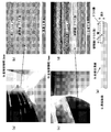
- FIG. 2 shows the silicon-based substrate processed in this way.
- FIG. 2A is a photograph of the outer periphery of the wafer ground at a width of 3 mm and a depth of 6 ⁇ m
- FIG. 2B is an enlarged photograph of FIG.
- FIG. 2 (c) is a photograph of the outer peripheral portion of the wafer ground at a width of 1 mm and a depth of 6 ⁇ m
- FIG. 2 (d) is an enlarged photograph of FIG. 2 (c).
- FIG. 2E is a cross-sectional view of the peripheral portion of the ground silicon substrate.
- the terrace surface may be made into a mirror surface or a semi-mirror surface by etching with a mixed acid or the like. By performing etching in this way to make the terrace surface a mirror surface or a quasi-mirror surface, dust generation can be suppressed and problems due to dust generation can be prevented.
- an epitaxial growth layer is formed on a silicon substrate set at 900 ° C. or higher, for example, 1200 ° C. using an epitaxial growth method such as metal organic chemical vapor deposition (MOCVD).
- MOCVD metal organic chemical vapor deposition
- the composition of the epitaxial layer is not particularly limited, but can be a nitride semiconductor, and the nitride semiconductor can be any one or more of AlN, AlGaN, and GaN.
- a buffer layer in which AlGaN layers and GaN layers are alternately stacked can be grown, and a GaN layer can be formed on the surface of the buffer layer, with a total thickness of about 3 to 10 ⁇ m. Can do.
- an epitaxial wafer is manufactured according to the manufacturing flow of FIG. 1 described above, a complete crack-free semiconductor epitaxial wafer can be easily obtained. In subsequent processes such as a device manufacturing process, cracks are extended or an epitaxial growth layer is formed. It is possible to prevent the production line from being contaminated by inducing peeling.
- the silicon substrate for epitaxial growth of the present invention is a silicon substrate for epitaxial growth for epitaxially growing a semiconductor layer, and the outer peripheral portion of the silicon substrate is terraced to have a terrace portion (FIG. 2 (e)). reference).
- the terrace surface of the terrace part is a mirror surface or a semi-mirror surface.
- the terrace surface of the terrace portion is a mirror surface or a quasi-mirror surface, dust generation from the terrace surface can be suppressed, and problems due to dust generation can be prevented.
- the semiconductor layer to be epitaxially grown can be made of a nitride semiconductor.
- the present invention can be suitably applied to a silicon substrate for epitaxial growth using a nitride semiconductor as a semiconductor layer to be epitaxially grown.
- the nitride semiconductor can be any one or more of AlN, GaN, InN, or a mixed crystal thereof.
- the present invention can be suitably applied to a silicon substrate for epitaxial growth using the above materials as a nitride semiconductor used for a semiconductor layer to be epitaxially grown.
- the epitaxial wafer of the present invention is obtained by growing an epitaxial layer on the above-mentioned epitaxial growth silicon substrate.
- An epitaxial wafer in which such an outer peripheral portion is terrace-processed and an epitaxial layer is grown on a silicon-based substrate having a terrace portion can be easily made into a complete crack-free epitaxial wafer.
- Example 2 The outer periphery of a silicon substrate having a diameter of 150 mm and a thickness of 1 mm was subjected to terrace processing by grinding at two levels of 3 mm in width, 6 ⁇ m in depth, and 50 ⁇ m using a grindstone having a particle size of # 3000. After an AlN layer was formed by epitaxial growth on a silicon substrate subjected to terrace processing, a buffer layer in which AlGaN layers and GaN layers were alternately stacked was epitaxially grown, and a GaN layer was epitaxially grown on the surface to produce an epitaxial wafer. The total thickness of the epitaxial layer was 10 ⁇ m.
- the present invention is not limited to the above embodiment.
- the above-described embodiment is an exemplification, and the present invention has substantially the same configuration as the technical idea described in the claims of the present invention, and any device that exhibits the same function and effect is the present invention. It is included in the technical scope of the invention.
Landscapes
- Chemical & Material Sciences (AREA)
- Engineering & Computer Science (AREA)
- Crystallography & Structural Chemistry (AREA)
- Materials Engineering (AREA)
- Metallurgy (AREA)
- Organic Chemistry (AREA)
- Chemical Kinetics & Catalysis (AREA)
- General Chemical & Material Sciences (AREA)
- Inorganic Chemistry (AREA)
- Chemical Vapour Deposition (AREA)
- Crystals, And After-Treatments Of Crystals (AREA)
Priority Applications (4)
| Application Number | Priority Date | Filing Date | Title |
|---|---|---|---|
| CN201580011736.1A CN106068547B (zh) | 2014-03-04 | 2015-02-10 | 外延晶圆的制造方法及外延生长用硅系基板 |
| DE112015000728.8T DE112015000728B4 (de) | 2014-03-04 | 2015-02-10 | Verfahren zum Herstellen eines epitaktischen Wafers und Substrat auf Siliziumbasis zum epitaktischen Wachstum |
| KR1020167024254A KR102262063B1 (ko) | 2014-03-04 | 2015-02-10 | 에피택셜 웨이퍼의 제조방법 및 에피택셜 성장용 실리콘계 기판 |
| US15/120,924 US10319587B2 (en) | 2014-03-04 | 2015-02-10 | Method of manufacturing epitaxial wafer and silicon-based substrate for epitaxial growth |
Applications Claiming Priority (2)
| Application Number | Priority Date | Filing Date | Title |
|---|---|---|---|
| JP2014041976A JP6157381B2 (ja) | 2014-03-04 | 2014-03-04 | エピタキシャルウェーハの製造方法及びエピタキシャルウェーハ |
| JP2014-041976 | 2014-03-04 |
Related Child Applications (1)
| Application Number | Title | Priority Date | Filing Date |
|---|---|---|---|
| US15/120,924 Continuation US10319587B2 (en) | 2014-03-04 | 2015-02-10 | Method of manufacturing epitaxial wafer and silicon-based substrate for epitaxial growth |
Publications (1)
| Publication Number | Publication Date |
|---|---|
| WO2015133063A1 true WO2015133063A1 (ja) | 2015-09-11 |
Family
ID=54054884
Family Applications (1)
| Application Number | Title | Priority Date | Filing Date |
|---|---|---|---|
| PCT/JP2015/000595 Ceased WO2015133063A1 (ja) | 2014-03-04 | 2015-02-10 | エピタキシャルウェーハの製造方法及びエピタキシャル成長用シリコン系基板 |
Country Status (7)
| Country | Link |
|---|---|
| US (1) | US10319587B2 (https=) |
| JP (1) | JP6157381B2 (https=) |
| KR (1) | KR102262063B1 (https=) |
| CN (1) | CN106068547B (https=) |
| DE (1) | DE112015000728B4 (https=) |
| TW (1) | TWI647326B (https=) |
| WO (1) | WO2015133063A1 (https=) |
Families Citing this family (2)
| Publication number | Priority date | Publication date | Assignee | Title |
|---|---|---|---|---|
| US10388518B2 (en) | 2017-03-31 | 2019-08-20 | Globalwafers Co., Ltd. | Epitaxial substrate and method of manufacturing the same |
| JP6879223B2 (ja) * | 2018-01-18 | 2021-06-02 | 株式会社Sumco | 貼り合わせウェーハの製造方法 |
Citations (3)
| Publication number | Priority date | Publication date | Assignee | Title |
|---|---|---|---|---|
| JPS6230336A (ja) * | 1985-07-31 | 1987-02-09 | Fujitsu Ltd | プラズマ酸化法 |
| JP2011119336A (ja) * | 2009-12-01 | 2011-06-16 | Mitsubishi Electric Corp | 半導体装置の製造方法およびそれに用いられる半導体基板 |
| JP2013118384A (ja) * | 2011-12-05 | 2013-06-13 | Samsung Electronics Co Ltd | シリコン基板、これを採用したエピ構造体及びシリコン基板の製造方法 |
Family Cites Families (13)
| Publication number | Priority date | Publication date | Assignee | Title |
|---|---|---|---|---|
| JPS59227117A (ja) | 1983-06-08 | 1984-12-20 | Nec Corp | 半導体装置 |
| JP3336866B2 (ja) * | 1996-08-27 | 2002-10-21 | 信越半導体株式会社 | 気相成長用シリコン単結晶基板の製造方法 |
| JP2007246289A (ja) | 2004-03-11 | 2007-09-27 | Nec Corp | 窒化ガリウム系半導体基板の作製方法 |
| JP2007204286A (ja) | 2006-01-31 | 2007-08-16 | Sumco Corp | エピタキシャルウェーハの製造方法 |
| TWI370184B (en) * | 2006-09-06 | 2012-08-11 | Sumco Corp | Epitaxial wafer and method of producing same |
| JP5029234B2 (ja) * | 2006-09-06 | 2012-09-19 | 株式会社Sumco | エピタキシャルウェーハの製造方法 |
| JP2011161975A (ja) | 2010-02-05 | 2011-08-25 | Toyota Motor Corp | 車両のパワートレーン |
| JP5417211B2 (ja) | 2010-02-10 | 2014-02-12 | Dowaエレクトロニクス株式会社 | エピタキシャル成長基板及び半導体装置、エピタキシャル成長方法 |
| JPWO2011161975A1 (ja) | 2010-06-25 | 2013-08-19 | Dowaエレクトロニクス株式会社 | エピタキシャル成長基板及び半導体装置、エピタキシャル成長方法 |
| JP6026188B2 (ja) | 2011-09-12 | 2016-11-16 | 住友化学株式会社 | 窒化物半導体結晶の製造方法 |
| JP6130995B2 (ja) | 2012-02-20 | 2017-05-17 | サンケン電気株式会社 | エピタキシャル基板及び半導体装置 |
| US10253432B2 (en) * | 2014-01-28 | 2019-04-09 | Sumitomo Chemical Company, Limited | Semiconductor substrate manufacturing method |
| JP6261388B2 (ja) * | 2014-03-05 | 2018-01-17 | 信越半導体株式会社 | 半導体エピタキシャルウェーハの製造方法 |
-
2014
- 2014-03-04 JP JP2014041976A patent/JP6157381B2/ja active Active
-
2015
- 2015-02-10 CN CN201580011736.1A patent/CN106068547B/zh active Active
- 2015-02-10 KR KR1020167024254A patent/KR102262063B1/ko active Active
- 2015-02-10 US US15/120,924 patent/US10319587B2/en active Active
- 2015-02-10 WO PCT/JP2015/000595 patent/WO2015133063A1/ja not_active Ceased
- 2015-02-10 DE DE112015000728.8T patent/DE112015000728B4/de active Active
- 2015-02-16 TW TW104105359A patent/TWI647326B/zh active
Patent Citations (3)
| Publication number | Priority date | Publication date | Assignee | Title |
|---|---|---|---|---|
| JPS6230336A (ja) * | 1985-07-31 | 1987-02-09 | Fujitsu Ltd | プラズマ酸化法 |
| JP2011119336A (ja) * | 2009-12-01 | 2011-06-16 | Mitsubishi Electric Corp | 半導体装置の製造方法およびそれに用いられる半導体基板 |
| JP2013118384A (ja) * | 2011-12-05 | 2013-06-13 | Samsung Electronics Co Ltd | シリコン基板、これを採用したエピ構造体及びシリコン基板の製造方法 |
Also Published As
| Publication number | Publication date |
|---|---|
| DE112015000728T5 (de) | 2017-05-11 |
| CN106068547B (zh) | 2019-06-04 |
| US20160365239A1 (en) | 2016-12-15 |
| KR102262063B1 (ko) | 2021-06-09 |
| TWI647326B (zh) | 2019-01-11 |
| CN106068547A (zh) | 2016-11-02 |
| TW201600621A (zh) | 2016-01-01 |
| DE112015000728B4 (de) | 2025-12-24 |
| JP6157381B2 (ja) | 2017-07-05 |
| JP2015170616A (ja) | 2015-09-28 |
| US10319587B2 (en) | 2019-06-11 |
| KR20160127748A (ko) | 2016-11-04 |
Similar Documents
| Publication | Publication Date | Title |
|---|---|---|
| JP6261388B2 (ja) | 半導体エピタキシャルウェーハの製造方法 | |
| JP4741572B2 (ja) | 窒化物半導体基板及びその製造方法 | |
| JP2012036030A (ja) | 半導体ウェハの製造方法 | |
| WO2010035409A1 (ja) | シリコンエピタキシャルウェーハの製造方法 | |
| JP6157381B2 (ja) | エピタキシャルウェーハの製造方法及びエピタキシャルウェーハ | |
| JP4130389B2 (ja) | Iii族窒化物系化合物半導体基板の製造方法 | |
| TWI861011B (zh) | 磊晶晶圓之製造方法、磊晶成長用矽基板及磊晶晶圓 | |
| WO2015067681A1 (en) | Epitaxial wafers avoiding edge melt-back-etching and method for fabricating the same | |
| US11680339B2 (en) | Method of manufacturing group III nitride semiconductor substrate, group III nitride semiconductor substrate, and bulk crystal | |
| JP7328230B2 (ja) | 半極性自立基板の製造方法 | |
| WO2023026847A1 (ja) | 窒化物半導体基板及びその製造方法 |
Legal Events
| Date | Code | Title | Description |
|---|---|---|---|
| 121 | Ep: the epo has been informed by wipo that ep was designated in this application |
Ref document number: 15758735 Country of ref document: EP Kind code of ref document: A1 |
|
| WWE | Wipo information: entry into national phase |
Ref document number: 15120924 Country of ref document: US |
|
| ENP | Entry into the national phase |
Ref document number: 20167024254 Country of ref document: KR Kind code of ref document: A |
|
| WWE | Wipo information: entry into national phase |
Ref document number: 112015000728 Country of ref document: DE |
|
| 122 | Ep: pct application non-entry in european phase |
Ref document number: 15758735 Country of ref document: EP Kind code of ref document: A1 |
|
| WWG | Wipo information: grant in national office |
Ref document number: 112015000728 Country of ref document: DE |