WO2015115657A1 - 接続体 - Google Patents
接続体 Download PDFInfo
- Publication number
- WO2015115657A1 WO2015115657A1 PCT/JP2015/052920 JP2015052920W WO2015115657A1 WO 2015115657 A1 WO2015115657 A1 WO 2015115657A1 JP 2015052920 W JP2015052920 W JP 2015052920W WO 2015115657 A1 WO2015115657 A1 WO 2015115657A1
- Authority
- WO
- WIPO (PCT)
- Prior art keywords
- conductive particles
- electrode
- substrate
- liquid crystal
- portions
- Prior art date
- Legal status (The legal status is an assumption and is not a legal conclusion. Google has not performed a legal analysis and makes no representation as to the accuracy of the status listed.)
- Ceased
Links
Images


Classifications
-
- H—ELECTRICITY
- H10—SEMICONDUCTOR DEVICES; ELECTRIC SOLID-STATE DEVICES NOT OTHERWISE PROVIDED FOR
- H10W—GENERIC PACKAGES, INTERCONNECTIONS, CONNECTORS OR OTHER CONSTRUCTIONAL DETAILS OF DEVICES COVERED BY CLASS H10
- H10W72/00—Interconnections or connectors in packages
- H10W72/071—Connecting or disconnecting
- H10W72/073—Connecting or disconnecting of die-attach connectors
-
- H—ELECTRICITY
- H10—SEMICONDUCTOR DEVICES; ELECTRIC SOLID-STATE DEVICES NOT OTHERWISE PROVIDED FOR
- H10W—GENERIC PACKAGES, INTERCONNECTIONS, CONNECTORS OR OTHER CONSTRUCTIONAL DETAILS OF DEVICES COVERED BY CLASS H10
- H10W72/00—Interconnections or connectors in packages
- H10W72/01—Manufacture or treatment
- H10W72/013—Manufacture or treatment of die-attach connectors
-
- H—ELECTRICITY
- H10—SEMICONDUCTOR DEVICES; ELECTRIC SOLID-STATE DEVICES NOT OTHERWISE PROVIDED FOR
- H10W—GENERIC PACKAGES, INTERCONNECTIONS, CONNECTORS OR OTHER CONSTRUCTIONAL DETAILS OF DEVICES COVERED BY CLASS H10
- H10W72/00—Interconnections or connectors in packages
- H10W72/071—Connecting or disconnecting
- H10W72/072—Connecting or disconnecting of bump connectors
-
- H—ELECTRICITY
- H10—SEMICONDUCTOR DEVICES; ELECTRIC SOLID-STATE DEVICES NOT OTHERWISE PROVIDED FOR
- H10W—GENERIC PACKAGES, INTERCONNECTIONS, CONNECTORS OR OTHER CONSTRUCTIONAL DETAILS OF DEVICES COVERED BY CLASS H10
- H10W72/00—Interconnections or connectors in packages
- H10W72/20—Bump connectors, e.g. solder bumps or copper pillars; Dummy bumps; Thermal bumps
-
- H—ELECTRICITY
- H10—SEMICONDUCTOR DEVICES; ELECTRIC SOLID-STATE DEVICES NOT OTHERWISE PROVIDED FOR
- H10W—GENERIC PACKAGES, INTERCONNECTIONS, CONNECTORS OR OTHER CONSTRUCTIONAL DETAILS OF DEVICES COVERED BY CLASS H10
- H10W72/00—Interconnections or connectors in packages
- H10W72/30—Die-attach connectors
-
- H—ELECTRICITY
- H10—SEMICONDUCTOR DEVICES; ELECTRIC SOLID-STATE DEVICES NOT OTHERWISE PROVIDED FOR
- H10W—GENERIC PACKAGES, INTERCONNECTIONS, CONNECTORS OR OTHER CONSTRUCTIONAL DETAILS OF DEVICES COVERED BY CLASS H10
- H10W72/00—Interconnections or connectors in packages
- H10W72/851—Dispositions of multiple connectors or interconnections
-
- H—ELECTRICITY
- H10—SEMICONDUCTOR DEVICES; ELECTRIC SOLID-STATE DEVICES NOT OTHERWISE PROVIDED FOR
- H10W—GENERIC PACKAGES, INTERCONNECTIONS, CONNECTORS OR OTHER CONSTRUCTIONAL DETAILS OF DEVICES COVERED BY CLASS H10
- H10W72/00—Interconnections or connectors in packages
- H10W72/01—Manufacture or treatment
- H10W72/013—Manufacture or treatment of die-attach connectors
- H10W72/01304—Manufacture or treatment of die-attach connectors using temporary auxiliary members, e.g. using sacrificial coatings or handle substrates
-
- H—ELECTRICITY
- H10—SEMICONDUCTOR DEVICES; ELECTRIC SOLID-STATE DEVICES NOT OTHERWISE PROVIDED FOR
- H10W—GENERIC PACKAGES, INTERCONNECTIONS, CONNECTORS OR OTHER CONSTRUCTIONAL DETAILS OF DEVICES COVERED BY CLASS H10
- H10W72/00—Interconnections or connectors in packages
- H10W72/01—Manufacture or treatment
- H10W72/013—Manufacture or treatment of die-attach connectors
- H10W72/01321—Manufacture or treatment of die-attach connectors using local deposition
- H10W72/01325—Manufacture or treatment of die-attach connectors using local deposition in solid form
-
- H—ELECTRICITY
- H10—SEMICONDUCTOR DEVICES; ELECTRIC SOLID-STATE DEVICES NOT OTHERWISE PROVIDED FOR
- H10W—GENERIC PACKAGES, INTERCONNECTIONS, CONNECTORS OR OTHER CONSTRUCTIONAL DETAILS OF DEVICES COVERED BY CLASS H10
- H10W72/00—Interconnections or connectors in packages
- H10W72/071—Connecting or disconnecting
- H10W72/072—Connecting or disconnecting of bump connectors
- H10W72/07221—Aligning
- H10W72/07223—Active alignment, e.g. using optical alignment using marks or sensors
-
- H—ELECTRICITY
- H10—SEMICONDUCTOR DEVICES; ELECTRIC SOLID-STATE DEVICES NOT OTHERWISE PROVIDED FOR
- H10W—GENERIC PACKAGES, INTERCONNECTIONS, CONNECTORS OR OTHER CONSTRUCTIONAL DETAILS OF DEVICES COVERED BY CLASS H10
- H10W72/00—Interconnections or connectors in packages
- H10W72/071—Connecting or disconnecting
- H10W72/073—Connecting or disconnecting of die-attach connectors
- H10W72/07321—Aligning
- H10W72/07323—Active alignment, e.g. using optical alignment using marks or sensors
-
- H—ELECTRICITY
- H10—SEMICONDUCTOR DEVICES; ELECTRIC SOLID-STATE DEVICES NOT OTHERWISE PROVIDED FOR
- H10W—GENERIC PACKAGES, INTERCONNECTIONS, CONNECTORS OR OTHER CONSTRUCTIONAL DETAILS OF DEVICES COVERED BY CLASS H10
- H10W72/00—Interconnections or connectors in packages
- H10W72/071—Connecting or disconnecting
- H10W72/073—Connecting or disconnecting of die-attach connectors
- H10W72/07331—Connecting techniques
- H10W72/07332—Compression bonding, e.g. thermocompression bonding
-
- H—ELECTRICITY
- H10—SEMICONDUCTOR DEVICES; ELECTRIC SOLID-STATE DEVICES NOT OTHERWISE PROVIDED FOR
- H10W—GENERIC PACKAGES, INTERCONNECTIONS, CONNECTORS OR OTHER CONSTRUCTIONAL DETAILS OF DEVICES COVERED BY CLASS H10
- H10W72/00—Interconnections or connectors in packages
- H10W72/071—Connecting or disconnecting
- H10W72/073—Connecting or disconnecting of die-attach connectors
- H10W72/07331—Connecting techniques
- H10W72/07337—Connecting techniques using a polymer adhesive, e.g. an adhesive based on silicone or epoxy
- H10W72/07338—Connecting techniques using a polymer adhesive, e.g. an adhesive based on silicone or epoxy hardening the adhesive by curing, e.g. thermosetting
-
- H—ELECTRICITY
- H10—SEMICONDUCTOR DEVICES; ELECTRIC SOLID-STATE DEVICES NOT OTHERWISE PROVIDED FOR
- H10W—GENERIC PACKAGES, INTERCONNECTIONS, CONNECTORS OR OTHER CONSTRUCTIONAL DETAILS OF DEVICES COVERED BY CLASS H10
- H10W72/00—Interconnections or connectors in packages
- H10W72/071—Connecting or disconnecting
- H10W72/074—Connecting or disconnecting of anisotropic conductive adhesives
-
- H—ELECTRICITY
- H10—SEMICONDUCTOR DEVICES; ELECTRIC SOLID-STATE DEVICES NOT OTHERWISE PROVIDED FOR
- H10W—GENERIC PACKAGES, INTERCONNECTIONS, CONNECTORS OR OTHER CONSTRUCTIONAL DETAILS OF DEVICES COVERED BY CLASS H10
- H10W72/00—Interconnections or connectors in packages
- H10W72/20—Bump connectors, e.g. solder bumps or copper pillars; Dummy bumps; Thermal bumps
- H10W72/221—Structures or relative sizes
- H10W72/222—Multilayered bumps, e.g. a coating on top and side surfaces of a bump core
-
- H—ELECTRICITY
- H10—SEMICONDUCTOR DEVICES; ELECTRIC SOLID-STATE DEVICES NOT OTHERWISE PROVIDED FOR
- H10W—GENERIC PACKAGES, INTERCONNECTIONS, CONNECTORS OR OTHER CONSTRUCTIONAL DETAILS OF DEVICES COVERED BY CLASS H10
- H10W72/00—Interconnections or connectors in packages
- H10W72/20—Bump connectors, e.g. solder bumps or copper pillars; Dummy bumps; Thermal bumps
- H10W72/231—Shapes
- H10W72/234—Cross-sectional shape, i.e. in side view
-
- H—ELECTRICITY
- H10—SEMICONDUCTOR DEVICES; ELECTRIC SOLID-STATE DEVICES NOT OTHERWISE PROVIDED FOR
- H10W—GENERIC PACKAGES, INTERCONNECTIONS, CONNECTORS OR OTHER CONSTRUCTIONAL DETAILS OF DEVICES COVERED BY CLASS H10
- H10W72/00—Interconnections or connectors in packages
- H10W72/20—Bump connectors, e.g. solder bumps or copper pillars; Dummy bumps; Thermal bumps
- H10W72/241—Dispositions, e.g. layouts
-
- H—ELECTRICITY
- H10—SEMICONDUCTOR DEVICES; ELECTRIC SOLID-STATE DEVICES NOT OTHERWISE PROVIDED FOR
- H10W—GENERIC PACKAGES, INTERCONNECTIONS, CONNECTORS OR OTHER CONSTRUCTIONAL DETAILS OF DEVICES COVERED BY CLASS H10
- H10W72/00—Interconnections or connectors in packages
- H10W72/20—Bump connectors, e.g. solder bumps or copper pillars; Dummy bumps; Thermal bumps
- H10W72/241—Dispositions, e.g. layouts
- H10W72/247—Dispositions of multiple bumps
- H10W72/248—Top-view layouts, e.g. mirror arrays
-
- H—ELECTRICITY
- H10—SEMICONDUCTOR DEVICES; ELECTRIC SOLID-STATE DEVICES NOT OTHERWISE PROVIDED FOR
- H10W—GENERIC PACKAGES, INTERCONNECTIONS, CONNECTORS OR OTHER CONSTRUCTIONAL DETAILS OF DEVICES COVERED BY CLASS H10
- H10W72/00—Interconnections or connectors in packages
- H10W72/20—Bump connectors, e.g. solder bumps or copper pillars; Dummy bumps; Thermal bumps
- H10W72/251—Materials
- H10W72/252—Materials comprising solid metals or solid metalloids, e.g. PbSn, Ag or Cu
-
- H—ELECTRICITY
- H10—SEMICONDUCTOR DEVICES; ELECTRIC SOLID-STATE DEVICES NOT OTHERWISE PROVIDED FOR
- H10W—GENERIC PACKAGES, INTERCONNECTIONS, CONNECTORS OR OTHER CONSTRUCTIONAL DETAILS OF DEVICES COVERED BY CLASS H10
- H10W72/00—Interconnections or connectors in packages
- H10W72/20—Bump connectors, e.g. solder bumps or copper pillars; Dummy bumps; Thermal bumps
- H10W72/251—Materials
- H10W72/255—Materials of outermost layers of multilayered bumps, e.g. material of a coating
-
- H—ELECTRICITY
- H10—SEMICONDUCTOR DEVICES; ELECTRIC SOLID-STATE DEVICES NOT OTHERWISE PROVIDED FOR
- H10W—GENERIC PACKAGES, INTERCONNECTIONS, CONNECTORS OR OTHER CONSTRUCTIONAL DETAILS OF DEVICES COVERED BY CLASS H10
- H10W72/00—Interconnections or connectors in packages
- H10W72/20—Bump connectors, e.g. solder bumps or copper pillars; Dummy bumps; Thermal bumps
- H10W72/261—Functions other than electrical connecting
-
- H—ELECTRICITY
- H10—SEMICONDUCTOR DEVICES; ELECTRIC SOLID-STATE DEVICES NOT OTHERWISE PROVIDED FOR
- H10W—GENERIC PACKAGES, INTERCONNECTIONS, CONNECTORS OR OTHER CONSTRUCTIONAL DETAILS OF DEVICES COVERED BY CLASS H10
- H10W72/00—Interconnections or connectors in packages
- H10W72/30—Die-attach connectors
- H10W72/321—Structures or relative sizes of die-attach connectors
- H10W72/325—Die-attach connectors having a filler embedded in a matrix
-
- H—ELECTRICITY
- H10—SEMICONDUCTOR DEVICES; ELECTRIC SOLID-STATE DEVICES NOT OTHERWISE PROVIDED FOR
- H10W—GENERIC PACKAGES, INTERCONNECTIONS, CONNECTORS OR OTHER CONSTRUCTIONAL DETAILS OF DEVICES COVERED BY CLASS H10
- H10W72/00—Interconnections or connectors in packages
- H10W72/30—Die-attach connectors
- H10W72/351—Materials of die-attach connectors
- H10W72/352—Materials of die-attach connectors comprising metals or metalloids, e.g. solders
-
- H—ELECTRICITY
- H10—SEMICONDUCTOR DEVICES; ELECTRIC SOLID-STATE DEVICES NOT OTHERWISE PROVIDED FOR
- H10W—GENERIC PACKAGES, INTERCONNECTIONS, CONNECTORS OR OTHER CONSTRUCTIONAL DETAILS OF DEVICES COVERED BY CLASS H10
- H10W72/00—Interconnections or connectors in packages
- H10W72/30—Die-attach connectors
- H10W72/351—Materials of die-attach connectors
- H10W72/353—Materials of die-attach connectors not comprising solid metals or solid metalloids, e.g. ceramics
-
- H—ELECTRICITY
- H10—SEMICONDUCTOR DEVICES; ELECTRIC SOLID-STATE DEVICES NOT OTHERWISE PROVIDED FOR
- H10W—GENERIC PACKAGES, INTERCONNECTIONS, CONNECTORS OR OTHER CONSTRUCTIONAL DETAILS OF DEVICES COVERED BY CLASS H10
- H10W72/00—Interconnections or connectors in packages
- H10W72/30—Die-attach connectors
- H10W72/351—Materials of die-attach connectors
- H10W72/353—Materials of die-attach connectors not comprising solid metals or solid metalloids, e.g. ceramics
- H10W72/354—Materials of die-attach connectors not comprising solid metals or solid metalloids, e.g. ceramics comprising polymers
-
- H—ELECTRICITY
- H10—SEMICONDUCTOR DEVICES; ELECTRIC SOLID-STATE DEVICES NOT OTHERWISE PROVIDED FOR
- H10W—GENERIC PACKAGES, INTERCONNECTIONS, CONNECTORS OR OTHER CONSTRUCTIONAL DETAILS OF DEVICES COVERED BY CLASS H10
- H10W72/00—Interconnections or connectors in packages
- H10W72/90—Bond pads, in general
- H10W72/921—Structures or relative sizes of bond pads
- H10W72/925—Bond pads having a filler embedded in a matrix
-
- H—ELECTRICITY
- H10—SEMICONDUCTOR DEVICES; ELECTRIC SOLID-STATE DEVICES NOT OTHERWISE PROVIDED FOR
- H10W—GENERIC PACKAGES, INTERCONNECTIONS, CONNECTORS OR OTHER CONSTRUCTIONAL DETAILS OF DEVICES COVERED BY CLASS H10
- H10W72/00—Interconnections or connectors in packages
- H10W72/90—Bond pads, in general
- H10W72/951—Materials of bond pads
-
- H—ELECTRICITY
- H10—SEMICONDUCTOR DEVICES; ELECTRIC SOLID-STATE DEVICES NOT OTHERWISE PROVIDED FOR
- H10W—GENERIC PACKAGES, INTERCONNECTIONS, CONNECTORS OR OTHER CONSTRUCTIONAL DETAILS OF DEVICES COVERED BY CLASS H10
- H10W74/00—Encapsulations, e.g. protective coatings
- H10W74/10—Encapsulations, e.g. protective coatings characterised by their shape or disposition
- H10W74/15—Encapsulations, e.g. protective coatings characterised by their shape or disposition on active surfaces of flip-chip devices, e.g. underfills
-
- H—ELECTRICITY
- H10—SEMICONDUCTOR DEVICES; ELECTRIC SOLID-STATE DEVICES NOT OTHERWISE PROVIDED FOR
- H10W—GENERIC PACKAGES, INTERCONNECTIONS, CONNECTORS OR OTHER CONSTRUCTIONAL DETAILS OF DEVICES COVERED BY CLASS H10
- H10W90/00—Package configurations
- H10W90/701—Package configurations characterised by the relative positions of pads or connectors relative to package parts
- H10W90/721—Package configurations characterised by the relative positions of pads or connectors relative to package parts of bump connectors
- H10W90/724—Package configurations characterised by the relative positions of pads or connectors relative to package parts of bump connectors between a chip and a stacked insulating package substrate, interposer or RDL
-
- H—ELECTRICITY
- H10—SEMICONDUCTOR DEVICES; ELECTRIC SOLID-STATE DEVICES NOT OTHERWISE PROVIDED FOR
- H10W—GENERIC PACKAGES, INTERCONNECTIONS, CONNECTORS OR OTHER CONSTRUCTIONAL DETAILS OF DEVICES COVERED BY CLASS H10
- H10W90/00—Package configurations
- H10W90/701—Package configurations characterised by the relative positions of pads or connectors relative to package parts
- H10W90/731—Package configurations characterised by the relative positions of pads or connectors relative to package parts of die-attach connectors
- H10W90/734—Package configurations characterised by the relative positions of pads or connectors relative to package parts of die-attach connectors between a chip and a stacked insulating package substrate, interposer or RDL
Definitions
- the present invention relates to a connection body in which an electronic component and a circuit board are connected, and particularly to a connection body in which the electronic component is connected to the circuit board through an adhesive containing conductive particles.
- liquid crystal display devices and organic EL panels have been used as various display means such as televisions, PC monitors, mobile phones, smart phones, portable game machines, tablet terminals, wearable terminals, and in-vehicle monitors.
- COG chip on glass
- a transparent electrode 102 made of ITO (indium tin oxide) or the like is provided on a transparent substrate 101 made of a glass substrate or the like.
- a plurality of such electronic components such as a liquid crystal driving IC 103 are connected on the transparent electrode 102.
- the liquid crystal driving IC 103 is formed with a plurality of electrode terminals 104 corresponding to the transparent electrodes 102 on the mounting surface, and thermocompression-bonded on the transparent substrate 101 via the anisotropic conductive film 105, thereby the electrode terminals 104. And the transparent electrode 102 are connected.
- the anisotropic conductive film 105 is a film formed by mixing conductive particles in a binder resin, and heat conduction is performed between the two conductors so that electrical conduction between the conductors is achieved with the conductive particles.
- the binder resin maintains the mechanical connection between the conductors.
- a highly reliable thermosetting binder resin is usually used, but a photocurable binder resin or a photothermal binder resin may be used.
- the anisotropic conductive film 105 is first attached to the transparent electrode 102 of the transparent substrate 101 by a temporary pressure bonding means (not shown). Temporarily stick. Subsequently, after mounting the liquid crystal driving IC 103 on the transparent substrate 101 via the anisotropic conductive film 105 to form a temporary connection body, the liquid crystal driving IC 103 is anisotropically formed by thermocompression bonding means such as a thermocompression bonding head 106. Heated and pressed to the transparent electrode 102 side together with the conductive film 105. By the heating by the thermocompression bonding head 106, the anisotropic conductive film 105 undergoes a thermosetting reaction, whereby the liquid crystal driving IC 103 is bonded onto the transparent electrode 102.
- thermocompression bonding head 106 Heated and pressed to the transparent electrode 102 side together with the conductive film 105.
- a protective film is formed on the surface of the circuit board to prevent physical damage or short circuit.
- substrate electrode currently formed in the substrate surface has the step part by producing
- a step portion is formed at the side edge portion of the metal electrode terminal.
- the stepped portion of the substrate electrode and the stepped portion of the electrode terminal are connected to each other.
- the conductive particles exist between the stepped portion of the substrate electrode and the stepped portion of the electrode terminal, the conductive particles are bitten between the two stepped portions, so that each main surface portion of the substrate electrode and the electrode terminal is sandwiched between them.
- the conductive particles could not be sufficiently crushed and the conductivity was impaired.
- the step portion of the substrate electrode is formed by a protective film, the conductivity is low, and the conductivity cannot be ensured by the conductive particles bitten between the two step portions.
- the diameter of the conductive particles is reduced, insufficient push-in of the conductive particles due to the conductive particles being bitten between the step portions of the substrate electrode and the electrode terminal appears more remarkably.
- anisotropic conductive films in which conductive particles are regularly arranged have been proposed in response to the finer pitch of circuit board wiring pitches and electrode terminals of electronic components. By doing so, the conductive particles can be reliably captured at the main surface portions of the substrate electrode and the electrode terminal, but the conductive particles may be easily bitten between the step portions.
- the present invention provides a conductive particle that is sandwiched between the main surface portions of the substrate electrode and the electrode terminal even when the conductive particle is bitten between the step portion of the substrate electrode and the step portion of the electrode terminal. It is an object of the present invention to provide a connection body between a circuit board and an electronic component that can be sufficiently pushed in to ensure electrical conductivity.
- a connection body includes a circuit board and an electronic component connected to the circuit board via an anisotropic conductive adhesive, and is formed on the circuit board.
- the electrode terminals formed on the substrate electrode and the electronic component are formed with step portions on each side edge, and the substrate electrode and the electrode terminal are formed between the main surface portions and on each side edge.
- the conductive particles contained in the anisotropic conductive adhesive are sandwiched between the stepped portions, and the conductive particles and the stepped portions of the substrate electrode and the electrode terminal are expressed by the following formula (1). It satisfies. a + b + c ⁇ 0.8D (1) [A: Step height of electrode terminal, b: Height of step portion of substrate electrode, c: Gap between steps, D: Diameter of conductive particles]
- the conductive particles sandwiched between both main surface portions of the substrate electrode and the electrode terminal can be compressed to at least 80% of the particle size, and sufficient electrical conductivity can be ensured.
- FIG. 1 is a cross-sectional view of a liquid crystal display panel shown as an example of a connection body.
- FIG. 2 is a cross-sectional view showing a connection process between the liquid crystal driving IC and the transparent substrate.
- FIG. 3 is a plan view showing electrode terminals (bumps) and inter-terminal spaces of the liquid crystal driving IC.
- FIG. 4 is a cross-sectional view showing an anisotropic conductive film.
- FIG. 5 is a plan view showing an anisotropic conductive film in which conductive particles are regularly arranged in a lattice shape.
- FIG. 6 is a cross-sectional view showing a substrate electrode and electrode terminals sandwiching conductive particles.
- FIG. 7 is a cross-sectional view showing a process of connecting the IC chip to the transparent substrate of the liquid crystal display panel, where (A) the process before connection and (B) the connection process.
- the liquid crystal display panel 10 includes two transparent substrates 11 and 12 made of a glass substrate and the like, and the transparent substrates 11 and 12 are bonded to each other by a frame-shaped seal 13. .
- the liquid crystal 14 is sealed in a space surrounded by the transparent substrates 11 and 12 to form a panel display unit 15.
- the transparent substrates 11 and 12 have a pair of striped transparent electrodes 16 and 17 made of ITO (Indium Tin Oxide) or the like on both inner surfaces facing each other so as to intersect each other.
- the transparent electrodes 16 and 17 are configured such that a pixel as a minimum unit of liquid crystal display is configured by the intersection of the transparent electrodes 16 and 17.
- one transparent substrate 12 is formed to have a larger planar dimension than the other transparent substrate 11, and an edge 12a of the formed transparent substrate 12 has an electronic component.
- a COG mounting unit 20 on which the liquid crystal driving IC 18 is mounted is provided.
- the COG mounting portion 20 is formed with a substrate-side alignment mark 21 that overlaps the terminal portion 17 a of the transparent electrode 17 and the IC-side alignment mark 22 provided on the liquid crystal driving IC 18.
- the transparent substrate 12 has an insulating protection made of an inorganic film or an organic film such as a nitride film or a silicon oxide film on the surface of the substrate in order to prevent physical damage or a short circuit.
- a film 23 is formed.
- the protective film 23 is formed in a region excluding the terminal portion 17a and the substrate side alignment mark 21 by a known film forming method.
- a step portion 28 is formed by the protective film 23 at the side edge of the terminal portion 17 a adjacent to the protective film 23.
- the terminal portion 17a has a stepped portion 28 protruding at both side edge portions in a cross-sectional view, and the main surface portion is flattened.
- the liquid crystal driving IC 18 can selectively apply a liquid crystal driving voltage to the pixels to change the alignment of the liquid crystal partially to perform a predetermined liquid crystal display.
- the liquid crystal driving IC 18 has a plurality of electrode terminals 19 (bumps) that are electrically connected to the terminal portions 17 a of the transparent electrode 17 on the mounting surface 18 a to the transparent substrate 12.
- the electrode terminal 19 for example, a copper bump, a gold bump, or a copper bump plated with gold is suitably used.
- the liquid crystal driving IC 18 includes electrode terminals 19 (input bumps) arranged in a line along one side edge of the mounting surface 18a, and the other side edge facing one side edge.
- the electrode terminals 19 (output bumps) are arranged in a zigzag manner in a plurality of rows.
- the electrode terminals 19 and the terminal portions 17a provided on the COG mounting portion 20 of the transparent substrate 12 are formed with the same number and the same pitch, respectively, and the transparent substrate 12 and the liquid crystal driving IC 18 are aligned and connected. Is connected.
- liquid crystal driving IC 18 With the recent miniaturization and higher functionality of liquid crystal display devices and other electronic devices, electronic components such as the liquid crystal driving IC 18 are also required to be smaller and lower in height, and the electrode terminal 19 is also lowered in height. (For example, 6 to 15 ⁇ m).
- the electrode terminal 19 has stepped portions 27 at both side edges.
- the stepped portion 27 is formed when the metal electrode terminal 19 is manufactured, and the electrode terminal 19 has both side edges raised and a main surface portion flattened in a sectional view.
- the liquid crystal driving IC 18 is anisotropically conductively connected to the COG mounting portion 20, so that the step portions 28 formed on both side edges of the electrode terminal 19 are formed on both side edges of the terminal portion 17a. 27. At this time, the terminal part 17a and the electrode terminal 19 are opposed to each other with a predetermined gap between the stepped parts 27 and 28, with the conductive particles 4 being bitten between them. The conductive particles 4 bitten between the two step portions 27 and 28 are largely crushed or broken between the two step portions 27 and 28 when the liquid crystal driving IC 18 is pressed by the thermocompression bonding head 33.
- the conductive particles 4 bitten between the two step portions 27 and 28 are largely crushed or broken between the two step portions 27 and 28 when the liquid crystal driving IC 18 is pressed by the thermocompression bonding head 33.
- each main surface part of the terminal part 17a and the electrode terminal 19 is at the height of both step parts 27 and 28, when the conductive particles 4 sandwiched between both step parts 27 and 28 are pressed (or broken). ) Are separated by a distance including the diameter.
- the height of the step portion 27 is the distance between the main surface portion extending in the normal direction of the main surface portion of the terminal portion 17 a and the top portion of the step portion 27, and the height of the step portion 28 is the main portion of the electrode terminal 19. The distance between the main surface portion over the normal direction of the surface portion and the top of the step portion 28 is said.
- the liquid crystal driving IC 18 is formed with an IC side alignment mark 22 for alignment with the transparent substrate 12 by being superimposed on the mounting surface 18a with the substrate side alignment mark 21. Since the wiring pitch of the transparent electrodes 17 of the transparent substrate 12 and the fine pitch of the electrode terminals 19 of the liquid crystal driving IC 18 are increasing, the liquid crystal driving IC 18 and the transparent substrate 12 are required to have high-precision alignment adjustment. It has been.
- the substrate-side alignment mark 21 and the IC-side alignment mark 22 various marks that can be aligned with the transparent substrate 12 and the liquid crystal driving IC 18 by being combined can be used.
- the liquid crystal driving IC 18 is connected to the terminal part 17a of the transparent electrode 17 formed in the COG mounting part 20 using the anisotropic conductive film 1 as an adhesive for circuit connection.
- the anisotropic conductive film 1 contains conductive particles 4, and the electrode terminal 19 of the liquid crystal driving IC 18 and the terminal portion 17 a of the transparent electrode 17 formed on the edge portion 12 a of the transparent substrate 12 are electrically conductive. Electrical connection is made through the particles 4.
- the anisotropic conductive film 1 is thermocompression bonded by the thermocompression bonding head 33, whereby the binder resin is fluidized and the conductive particles 4 are crushed between the terminal portion 17a and the electrode terminal 19 of the liquid crystal driving IC 18. In this state, the binder resin is cured. Thereby, the anisotropic conductive film 1 electrically and mechanically connects the transparent substrate 12 and the liquid crystal driving IC 18.
- an alignment film 24 subjected to a predetermined rubbing process is formed on both the transparent electrodes 16 and 17, and the initial alignment of liquid crystal molecules is regulated by the alignment film 24.
- a pair of polarizing plates 25 and 26 are disposed outside the transparent substrates 11 and 12, and these polarizing plates 25 and 26 allow transmitted light from a light source (not shown) such as a backlight to be transmitted. The vibration direction is regulated.
- an anisotropic conductive film (ACF) 1 usually has a binder resin layer (adhesive layer) 3 containing conductive particles 4 on a release film 2 as a base material. It is formed.
- the anisotropic conductive film 1 is a thermosetting adhesive or a photo-curing adhesive such as ultraviolet rays, and is attached to the transparent electrode 17 formed on the transparent substrate 12 of the liquid crystal display panel 10 and also has a liquid crystal driving IC 18.
- the anisotropic conductive film 1 can connect the transparent substrate 12 and the liquid crystal driving IC 18 to make them conductive.
- the anisotropic conductive film 1 has a normal binder resin layer 3 and conductive particles 4 containing a film-forming resin, a thermosetting resin, a latent curing agent, a silane coupling agent, and the like. As shown in FIG. 4, in the anisotropic conductive film 1, it is preferable that the conductive particles 4 are regularly arranged in a predetermined pattern on the binder resin layer 3.
- the release film 2 that supports the binder resin layer 3 is made of, for example, PET (Poly (Ethylene Terephthalate), OPP (Oriented Polypropylene), PMP (Poly-4-methylpentene-1), PTFE (Polytetrafluoroethylene) or the like with a release agent such as silicone. It coats and prevents the anisotropic conductive film 1 from drying, and maintains the shape of the anisotropic conductive film 1.
- the film-forming resin contained in the binder resin layer 3 is preferably a resin having an average molecular weight of about 10,000 to 80,000.
- the film forming resin include various resins such as an epoxy resin, a modified epoxy resin, a urethane resin, and a phenoxy resin. Among these, phenoxy resin is particularly preferable from the viewpoint of film formation state, connection reliability, and the like.
- thermosetting resin is not particularly limited, and examples thereof include commercially available epoxy resins and acrylic resins.
- the epoxy resin is not particularly limited.
- naphthalene type epoxy resin biphenyl type epoxy resin, phenol novolac type epoxy resin, bisphenol type epoxy resin, stilbene type epoxy resin, triphenolmethane type epoxy resin, phenol aralkyl type epoxy resin.
- an acrylic compound, liquid acrylate, etc. can be selected suitably.
- what made acrylate the methacrylate can also be selected from methyl acrylate, ethyl acrylate, isopropy
- the latent curing agent is not particularly limited, and examples thereof include various curing agents such as a heat curing type and a UV curing type.
- the latent curing agent does not normally react, but is activated by various triggers selected according to applications such as heat, light, and pressure, and starts the reaction.
- the activation method of the thermal activation type latent curing agent includes a method of generating active species (cation, anion, radical) by a dissociation reaction by heating, etc., and it is stably dispersed in the epoxy resin near room temperature, and epoxy at high temperature
- active species cation, anion, radical
- Thermally active latent curing agents include imidazole, hydrazide, boron trifluoride-amine complexes, sulfonium salts, amine imides, polyamine salts, dicyandiamide, etc., and modified products thereof. The above mixture may be sufficient. Among these, a microcapsule type imidazole-based latent curing agent is preferable.
- the silane coupling agent is not particularly limited, and examples thereof include an epoxy type, an amino type, a mercapto sulfide type, and a ureido type. By adding the silane coupling agent, the adhesion at the interface between the organic material and the inorganic material is improved.
- Examples of the conductive particles 4 include any known conductive particles used in the anisotropic conductive film 1.
- Examples of the conductive particles 4 include particles of various metals and metal alloys such as nickel, iron, copper, aluminum, tin, lead, chromium, cobalt, silver, gold, metal oxide, carbon, graphite, glass, ceramic, Examples thereof include those in which the surface of particles such as plastic is coated with metal, or those in which the surface of these particles is further coated with an insulating thin film.
- examples of the resin particle include an epoxy resin, a phenol resin, an acrylic resin, an acrylonitrile / styrene (AS) resin, a benzoguanamine resin, a divinylbenzene resin, a styrene resin, and the like. Can be mentioned.
- the anisotropic conductive film 1 it is preferable that the conductive particles 4 are regularly arranged in a predetermined arrangement pattern in a plan view, and for example, as shown in FIG.
- the anisotropic conductive film 1 has a finer space between the adjacent electrode terminals 19 of the liquid crystal driving IC 18 than when the conductive particles 4 are randomly dispersed. Even when the pitch is reduced and the area between the terminals is reduced, and the conductive particles 4 are filled with high density, the short circuit between the electrode terminals 19 due to the aggregate of the conductive particles 4 is prevented in the connection process of the liquid crystal driving IC 18. can do.
- the anisotropic conductive film 1 prevents the occurrence of density due to aggregation of the conductive particles 4 even when the binder resin layer 3 is filled with high density by arranging the conductive particles 4 regularly. Has been. Therefore, according to the anisotropic conductive film 1, the conductive particles 4 can be captured even in the terminal portions 17 a and the electrode terminals 19 that are fine pitched.
- the uniform arrangement pattern of the conductive particles 4 can be arbitrarily set to a lattice shape or the like in plan view. The connection process of the liquid crystal driving IC 18 will be described in detail later.
- an anisotropic conductive film 1 for example, a pressure-sensitive adhesive is applied on a stretchable sheet, the conductive particles 4 are arranged in a single layer thereon, and then the sheet is stretched at a desired stretch ratio.
- the shape of the anisotropic conductive film 1 is not particularly limited.
- the anisotropic conductive film 1 is cut by a predetermined length by forming a long tape shape that can be wound around the take-up reel 6. Can be used.
- molded the thermosetting resin composition which regularly arranged the electroconductive particle 4 in the binder resin layer 3 as the anisotropic conductive film 1 in the film form is not limited to this.
- an insulating adhesive layer made of only the binder resin 3 and a conductive particle-containing layer made of the binder resin 3 in which the conductive particles 4 are regularly arranged are laminated. It can be configured.
- the anisotropic conductive film 1 is arranged in a single layer as shown in FIG. 4, and the conductive particles 4 extend over a plurality of binder resin layers 3. May be arranged and regularly arranged in a plan view.
- the anisotropic conductive film 1 may be a single dispersion at a predetermined distance in at least one layer of a multilayer structure.
- the liquid crystal display panel 10 compresses the conductive particles 4 sandwiched between both main surface portions of the terminal portion 17a and the electrode terminal 19 until it becomes at least 80% of the particle size when uncompressed. And sufficient electrical conductivity can be ensured.
- the conductive particles 4 bite between the step portion 27 of the electrode terminal 19 and the step portion 28 of the terminal portion 17 a. I'm stuck.
- the distance between both main surface portions of the terminal portion 17a and the electrode terminal 19 is such that the step height a of the electrode terminal 19, the step height b of the terminal portion 17a, and the conductive particles 4 are bitten.
- a distance obtained by adding the gap c between the two stepped portions 27 and 28 (a + b + c) is obtained.
- the distance (a + b + c) between both main surface portions of the terminal portion 17a and the electrode terminal 19 is 80% or less of the diameter D of the conductive particles 4, so that the conductive particles 4 are at least 80% or less of the particle size. Can be pushed in until compressed.
- the conductive particles 4 are bitten between the step portion 27 of the electrode terminal 19 and the step portion 28 of the terminal portion 17a, so that both of the terminal portion 17a and the electrode terminal 19 are present.
- the distance between the main surface portions is at least larger than 80% of the particle diameter of the conductive particles 4, and the compressibility of the conductive particles 4 is less than 20%, so that the pushing is insufficient. Therefore, there is a possibility that the electrical conductivity between the terminal portion 17a and the electrode terminal 19 is deteriorated.
- the conductive particles 4 to be bitten between the step portion 27 of the terminal portion 17a and the step portion 28 of the electrode terminal 19 are applied with a pressure larger than that sandwiched between the main surface portions, Compressed to a particle size of approximately 1 ⁇ m or less.
- the conductive particles 4 have a size of approximately 1 ⁇ m or less even when broken by compression. That is, the gap c between both stepped portions 27 and 28 is 1 ⁇ m or less.
- connection process Next, a connection process for connecting the liquid crystal driving IC 18 to the transparent substrate 12 will be described.
- the anisotropic conductive film 1 is temporarily attached on the COG mounting part 20 in which the terminal part 17a of the transparent substrate 12 is formed.
- the transparent substrate 12 is placed on the stage of the connection device, and the liquid crystal driving IC 18 is disposed on the mounting portion of the transparent substrate 12 via the anisotropic conductive film 1.
- thermocompression bonding head 33 heated to a predetermined temperature for curing the binder resin layer 3 is hot-pressed from above the liquid crystal driving IC 18 at a predetermined pressure and time.
- the binder resin layer 3 of the anisotropic conductive film 1 exhibits fluidity, and flows out from between the mounting surface 18a of the liquid crystal driving IC 18 and the COG mounting portion 20 of the transparent substrate 12, and in the binder resin layer 3.
- the conductive particles 4 are sandwiched between the electrode terminals 19 of the liquid crystal driving IC 18 and the terminal portions 17a of the transparent substrate 12 and are crushed.
- the liquid crystal display panel 10 can compress the conductive particles 4 sandwiched between both main surface portions of the terminal portion 17a and the electrode terminal 19 until at least 80% of the particle size is reached, and ensure sufficient electrical conductivity. can do.
- the liquid crystal display panel 10 uses the anisotropic conductive film 1 filled with a high density by regularly arranging conductive particles corresponding to the fine pitch of the terminal portions 17a and the electrode terminals 19, the terminals The phenomenon that the conductive particles 4 are bitten between the step portions 27 and 28 as well as the main surface portions of the portion 17a and the electrode terminal 19 is likely to occur. Also in this case, by satisfying the above formula (1), the conductive particles 4 sandwiched between the main surface portions of the terminal portion 17a and the electrode terminal 19 can be compressed by 20% or more, and good conduction reliability is achieved. Can be secured.
- the conductive particles 4 are electrically connected between the electrode terminals 19 and the terminal portions 17a, and in this state, the binder resin heated by the thermocompression bonding head 33 is cured. Thereby, the liquid crystal display panel 10 in which electrical conductivity is ensured between the electrode terminal 19 of the liquid crystal driving IC 18 and the terminal portion 17a formed on the transparent substrate 12 can be manufactured.
- the conductive particles 4 that are not between the electrode terminals 19 and the terminal portions 17a are dispersed in the binder resin in the inter-terminal spaces between the adjacent electrode terminals 19, and maintain an electrically insulated state. Thereby, electrical conduction is achieved only between the electrode terminal 19 of the liquid crystal driving IC 18 and the terminal portion 17a of the transparent substrate 12.
- the binder resin can be rapidly cured even with a short heating time.
- the anisotropic conductive film 1 is not limited to the thermosetting type, and may be a photo-curing type or a photo-heat combined type adhesive as long as pressure connection is performed.
- a connected body sample in which an evaluation IC was connected to an evaluation glass substrate was prepared using an anisotropic conductive film in which conductive particles were regularly arranged, and each substrate was formed on the evaluation glass substrate.
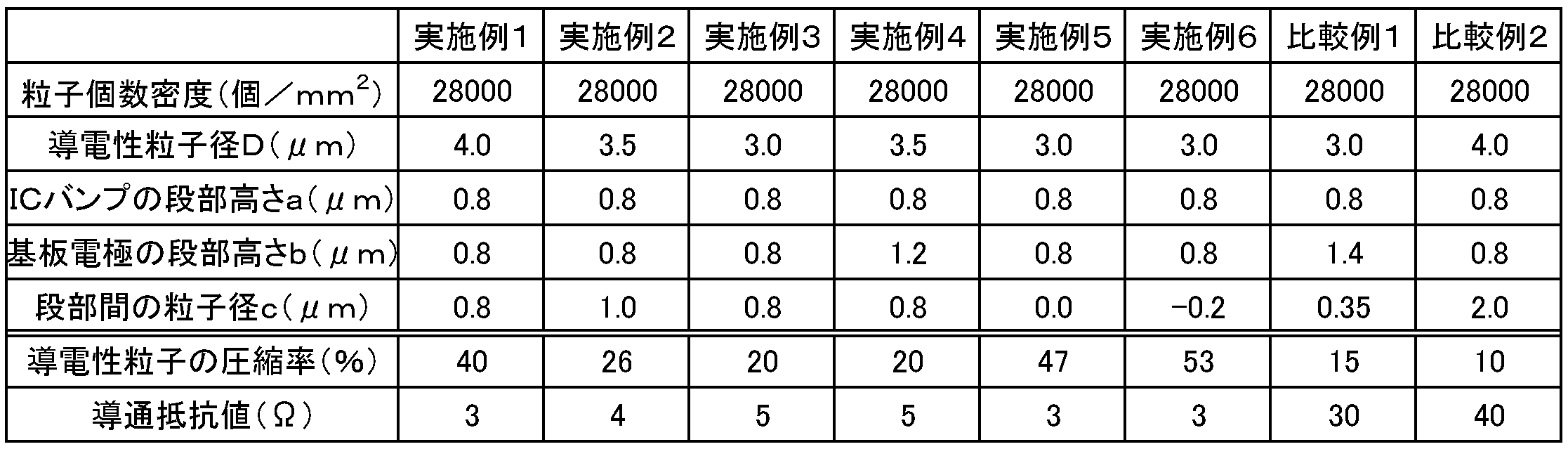
- Conductivity resistance Examples 1 to 6 and Comparative Examples 1 and 2 after the reliability test of the conductive particles trapped between the electrodes and the IC bumps formed on the evaluation IC or adjacent IC bumps
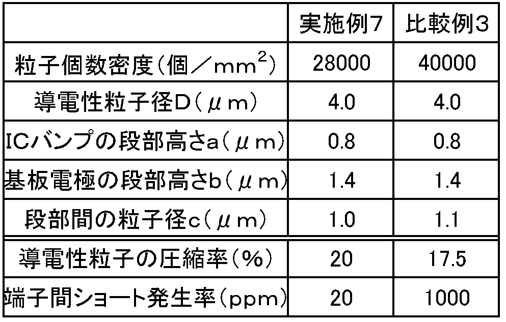
- the short-circuit occurrence rate Example 7, Comparative Example 3 was measured.
- the binder resin layer of the anisotropic conductive film used for connecting the IC for evaluation was 60 parts by mass of phenoxy resin (trade name: YP50, manufactured by Nippon Steel Chemical Co., Ltd.), epoxy resin (trade name: jER828, manufactured by Mitsubishi Chemical Corporation).
- a binder resin composition prepared by adding 40 parts by mass and 2 parts by mass of a cationic curing agent (trade name: SI-60L, manufactured by Sanshin Chemical Industry Co., Ltd.) to a solvent is prepared, and this binder resin composition is applied onto a release film. It was formed by firing.
- IC for evaluation As an evaluation element for measuring the conduction resistance, an outer shape: 1.8 mm ⁇ 20 mm, a thickness of 0.5 mm, a bump (Au-plated); a width of 30 ⁇ x, a length of 85 ⁇ m, a height of 15 ⁇ m, and a space width between bumps: evaluation of 50 ⁇ m IC was used.
- evaluation glass substrate As an evaluation glass substrate to which an evaluation IC for measuring conduction resistance is connected, an outer shape: 30 mm ⁇ 50 mm, a thickness of 0.5 mm, and a comb having the same size and pitch as the bumps of the evaluation IC for measuring conduction resistance An ITO pattern glass in which a tooth-like electrode pattern was formed and a protective film was formed in a region excluding the electrode pattern was used.
- IC for evaluation As an evaluation element for measuring the short-circuit occurrence rate between adjacent IC bumps, outer shape: 1.5 mm ⁇ 13 mm, thickness 0.5 mm, bump (Au-plated); width 25 ⁇ ⁇ length 140 ⁇ m, height 15 ⁇ m, bump An evaluation IC having a space width of 7.5 ⁇ m was used.
- an evaluation glass substrate As an evaluation glass substrate to which an evaluation IC for measuring a short-circuit occurrence rate between adjacent IC bumps is connected, an outer shape: 30 mm ⁇ 50 mm, a thickness of 0.5 mm, and a short-circuit occurrence rate between adjacent IC bumps are measured.
- An ITO pattern glass having a comb-like electrode pattern having the same size and pitch as the bumps of the evaluation IC and a protective film formed in a region excluding the electrode pattern was used.
- thermocompression bonding head After an anisotropic conductive film was temporarily pasted on these evaluation glass substrates, the evaluation IC was mounted while aligning the IC bumps and the substrate electrodes, and was crimped by a thermocompression bonding head.
- Comparative Example 1 and Comparative Example 3 connected body samples were prepared by thermocompression bonding under the conditions of 180 ° C., 80 MPa, and 5 seconds.
- Comparative Example 2 a connected body sample was prepared by thermocompression bonding under conditions of 180 ° C., 40 MPa, and 5 seconds.
- connection body sample the compression rate of the electroconductive particle currently pinched
- the conditions of the reliability test are 85 ° C., 85% RH, and 500 hr.
- Example 1 In Example 1, conductive particles having a particle diameter of 4 ⁇ m were used as the anisotropic conductive film. The particle number density before connection is 28000 / mm 2 . The height a of the step formed on the side edge of the IC bump is 0.8 ⁇ m, and the height b of the step formed on the side edge of the substrate electrode formed on the glass substrate is 0.8 ⁇ m. is there.
- connection body sample according to Example 1 the gap c between the step portions due to the conductive particles being bitten between the step portions of the IC bump and the substrate electrode is 0.8 ⁇ m.
- the compressibility of the conductive particles sandwiched between the face portions was 40%, and the conduction resistance after the reliability test was 3 ⁇ .
- Example 2 In Example 2, an anisotropic conductive film using conductive particles having a particle diameter of 3.5 ⁇ m was used. The particle number density before connection is 28000 / mm 2 . The heights a and b of each step of the IC bump and the substrate electrode were the same as those in Example 1.
- the gap c between the step portions due to the conductive particles being bitten between the step portions of the IC bump and the substrate electrode is 1.0 ⁇ m.
- the compressibility of the conductive particles sandwiched between the surface portions was 26%, and the conduction resistance after the reliability test was 4 ⁇ .
- Example 3 In Example 3, an anisotropic conductive film using conductive particles having a particle diameter of 3.0 ⁇ m was used. The particle number density before connection is 28000 / mm 2 . The heights a and b of each step of the IC bump and the substrate electrode were the same as those in Example 1.
- the gap c between the step portions due to the conductive particles being bitten between the step portions of the IC bump and the substrate electrode is 0.8 ⁇ m.
- the compressibility of the conductive particles sandwiched between the surface portions was 20%, and the conduction resistance after the reliability test was 5 ⁇ .
- Example 4 In Example 4, an anisotropic conductive film using conductive particles having a particle diameter of 3.5 ⁇ m was used.
- the particle number density before connection is 28000 / mm 2 .
- the height a of the step formed on the side edge of the IC bump is 0.8 ⁇ m, and the height b of the step formed on the side edge of the substrate electrode formed on the glass substrate is 1.2 ⁇ m. is there.
- the gap c between the step portions due to the conductive particles being bitten between the step portions of the IC bump and the substrate electrode is 0.8 ⁇ m.
- the compressibility of the conductive particles sandwiched between the surface portions was 20%, and the conduction resistance after the reliability test was 5 ⁇ .
- Example 5 In Example 5, an anisotropic conductive film using conductive particles having a particle diameter of 3.0 ⁇ m was used. The particle number density before connection is 28000 / mm 2 . The heights a and b of each step of the IC bump and the substrate electrode were the same as those in Example 1.
- connection body sample according to Example 5 the conductive particles are not bitten between the IC bump and the substrate electrode, the gap c between the steps is 0 ⁇ m, and the IC bump and the substrate electrode are between the main surface portions.
- the compression ratio of the sandwiched conductive particles was 47%, and the conduction resistance after the reliability test was 3 ⁇ .
- Example 6 In Example 6, an anisotropic conductive film using conductive particles having a particle diameter of 3.0 ⁇ m was used. The particle number density before connection is 28000 / mm 2 . The heights a and b of each step of the IC bump and the substrate electrode were the same as those in Example 1.
- the gap c between the stepped portions is ⁇ 0.2 ⁇ m due to a shift between the side edge of the IC bump and the side edge of the substrate electrode.
- the compressibility of the conductive particles sandwiched between the main surface portions was 53%, and the conduction resistance after the reliability test was 3 ⁇ .
- Example 7 In Example 7, an anisotropic conductive film using conductive particles having a particle diameter of 4.0 ⁇ m was used.
- the particle number density before connection is 28000 / mm 2 .
- the height a of the step formed on the side edge of the IC bump is 0.8 ⁇ m, and the height b of the step formed on the side edge of the substrate electrode formed on the glass substrate is 1.4 ⁇ m. is there.
- the gap c between the step portions due to the conductive particles being bitten between the step portions of the IC bump and the substrate electrode is 1.0 ⁇ m.
- the compressibility of the conductive particles sandwiched between the surface portions was 20%, and the incidence rate of terminal shorting between adjacent IC bumps was 20 ppm.
- Comparative Example 1 In Comparative Example 1, an anisotropic conductive film using conductive particles having a particle diameter of 3.0 ⁇ m was used. The particle number density before connection is 28000 / mm 2 . The height a of the step formed on the side edge of the IC bump is 0.8 ⁇ m, and the height b of the step formed on the side edge of the substrate electrode formed on the glass substrate is 1.4 ⁇ m. is there.
- connection body sample according to Comparative Example 1 the gap c between the step portions due to the conductive particles being bitten between the step portions of the IC bump and the substrate electrode is 0.35 ⁇ m.
- the compressibility of the conductive particles sandwiched between the surface portions was 15%, and the conduction resistance after the reliability test was 30 ⁇ .
- Comparative Example 2 In Comparative Example 2, an anisotropic conductive film using conductive particles having a particle diameter of 4.0 ⁇ m was used. The particle number density before connection is 28000 / mm 2 . The height a of the step formed on the side edge of the IC bump is 0.8 ⁇ m, and the height b of the step formed on the side edge of the substrate electrode formed on the glass substrate is 0.8 ⁇ m. is there.
- connection body sample according to Comparative Example 2 the gap c between the step portions due to the conductive particles being bitten between the step portions of the IC bump and the substrate electrode by reducing the pressing force of the thermocompression bonding head to 40 MPa.
- the compressibility of the conductive particles sandwiched between both main surface portions of the IC bump and the substrate electrode was 10%, and the conduction resistance after the reliability test was 40 ⁇ .
- Comparative Example 3 In Comparative Example 3, an anisotropic conductive film using conductive particles having a particle diameter of 4.0 ⁇ m was used. The particle number density before connection is 40,000 particles / mm 2 . The height a of the step formed on the side edge of the IC bump is 0.8 ⁇ m, and the height b of the step formed on the side edge of the substrate electrode formed on the glass substrate is 1.4 ⁇ m. is there.
- the gap c between the step portions due to the conductive particles being bitten between the IC bump and the step portion of the substrate electrode is 1.1 ⁇ m.
- the compressibility of the conductive particles sandwiched between the surface portions was 17.5%, and the occurrence rate of terminal shorts between adjacent IC bumps was 1000 ppm.
- the height a of the step formed on the side edge of the IC bump and the height of the step formed on the edge of the substrate electrode formed on the glass substrate is 80% or less of the diameter of the conductive particles. Therefore, in Examples 1 to 6, the conductive particles sandwiched between the main surface portions of the IC bump and the substrate electrode are compressed by 20% or more, and good conductivity can be maintained even after the reliability test.
- Comparative Example 1 the distance between both main surface portions of the IC bump and the substrate electrode was as wide as 85% of the diameter of the conductive particles, and the conductive particles were compressed only to 15%.
- Comparative Example 2 the distance between both main surface portions of the IC bump and the substrate electrode was as wide as 90% of the diameter of the conductive particles, and the conductive particles were compressed only to 10%. Therefore, in Comparative Example 1 and Comparative Example 2, the pushing of the conductive particles was insufficient, and the conductivity was greatly deteriorated with a conduction resistance of 30 ⁇ or more after the reliability test.
- Example 7 the particle number density of Example 7 is 28000 / mm 2 whereas the particle number density of Comparative Example 3 is packed at a high density of 40000 / mm 2 .
- the connection sample according to Example 7 has an average inter-particle distance in the space between the IC bumps of 2 ⁇ m (0.5 times the particle diameter), whereas the connection sample according to Comparative Example 3 The distance between particles in the space between IC bumps is as narrow as 1 ⁇ m on average (0.25 times the particle diameter).
- the conductive particles bitten between the step portions of the IC bump and the substrate electrode are also connected, and in Comparative Example 3, the incidence of shorting between the IC bumps is greatly increased as compared with Example 7.
- thermocompression bonding head 1 anisotropic conductive film, 2 release film, 3 binder resin layer, 4 conductive particles, 6 take-up reel, 10 liquid crystal display panel, 11, 12 transparent substrate, 12a edge, 13 seal, 14 liquid crystal, 15 panel display Part, 16, 17 transparent electrode, 17a terminal part, 18 liquid crystal driving IC, 18a mounting surface, 19 electrode terminal, 20 COG mounting part, 21 substrate side alignment mark, 22 IC side alignment mark, 23 protective film, 27, 28 Step, 33 thermocompression bonding head
Landscapes
- Wire Bonding (AREA)
- Liquid Crystal (AREA)
- Engineering & Computer Science (AREA)
- Manufacturing & Machinery (AREA)
- Electric Connection Of Electric Components To Printed Circuits (AREA)
Abstract
Description
a+b+c≦0.8D ・・・(1)
[a:電極端子の段部高さ、b:基板電極の段部高さ、c:段部間ギャップ、D:導電性粒子の径]
以下では、本発明が適用された接続体として、ガラス基板に、電子部品として液晶駆動用のICチップが実装された液晶表示パネルを例に説明する。この液晶表示パネル10は、図1に示すように、ガラス基板等からなる二枚の透明基板11,12が対向配置され、これら透明基板11,12が枠状のシール13によって互いに貼り合わされている。そして、液晶表示パネル10は、透明基板11,12によって囲繞された空間内に液晶14が封入されることによりパネル表示部15が形成されている。
また、図2に示すように、透明基板12は、物理的な損傷や短絡等を防止するために、基板表面に窒化膜や酸化シリコン膜などの無機膜や有機膜などからなる絶縁性の保護膜23が形成されている。保護膜23は、公知の成膜手法により、端子部17aや基板側アライメントマーク21を除く領域に形成されている。これにより、保護膜23と隣接する端子部17aの側縁部には保護膜23による段部28が形成される。したがって、端子部17aは、断面視において、両側縁部において段部28が隆起し、主面部が平坦化されている。
液晶駆動用IC18は、例えば、図3に示すように、実装面18aの一方の側縁に沿って電極端子19(入力バンプ)が一列で配列され、一方の側縁と対向する他方の側縁に沿って電極端子19(出力バンプ)が複数列で千鳥状に配列されている。電極端子19と、透明基板12のCOG実装部20に設けられている端子部17aとは、それぞれ同数かつ同ピッチで形成され、透明基板12と液晶駆動用IC18とが位置合わせされて接続されることにより、接続される。
次いで、異方性導電フィルム1について説明する。異方性導電フィルム(ACF:Anisotropic Conductive Film)1は、図4に示すように、通常、基材となる剥離フィルム2上に導電性粒子4を含有するバインダー樹脂層(接着剤層)3が形成されたものである。異方性導電フィルム1は、熱硬化型あるいは紫外線等の光硬化型の接着剤であり、液晶表示パネル10の透明基板12に形成された透明電極17上に貼着されるとともに液晶駆動用IC18が搭載され、熱圧着ヘッド33により熱加圧されることにより流動化して導電性粒子4が相対向する透明電極17の端子部17aと液晶駆動用IC18の電極端子19との間で押し潰され、加熱あるいは紫外線照射により、導電性粒子が押し潰された状態で硬化する。これにより、異方性導電フィルム1は、透明基板12と液晶駆動用IC18とを接続し、導通させることができる。
導電性粒子4としては、異方性導電フィルム1において使用されている公知の何れの導電性粒子を挙げることができる。導電性粒子4としては、例えば、ニッケル、鉄、銅、アルミニウム、錫、鉛、クロム、コバルト、銀、金等の各種金属や金属合金の粒子、金属酸化物、カーボン、グラファイト、ガラス、セラミック、プラスチック等の粒子の表面に金属をコートしたもの、或いは、これらの粒子の表面に更に絶縁薄膜をコートしたもの等が挙げられる。樹脂粒子の表面に金属をコートしたものである場合、樹脂粒子としては、例えば、エポキシ樹脂、フェノール樹脂、アクリル樹脂、アクリロニトリル・スチレン(AS)樹脂、ベンゾグアナミン樹脂、ジビニルベンゼン系樹脂、スチレン系樹脂等の粒子を挙げることができる。
異方性導電フィルム1は、導電性粒子4が平面視において所定の配列パターンで規則的に配列され、例えば図5に示すように、格子状かつ均等に配列されることが好ましい。平面視において規則的に配列されることにより、異方性導電フィルム1は、導電性粒子4がランダムに分散されている場合に比して、液晶駆動用IC18の隣接する電極端子19間がファインピッチ化し端子間面積が狭小化するとともに、導電性粒子4が高密度に充填されていても、液晶駆動用IC18の接続工程において、導電性粒子4の凝集体による電極端子19間のショートを防止することができる。
ここで、導電性粒子4を規則配列した異方性導電フィルム1を用いた場合、図6に示すように、電極端子19及び端子部17aの両段部27,28間に導電性粒子4が咬みこまれる場合がある。このとき、導電性粒子4と、導電性粒子4を挟持する電極端子19及び端子部17aの各段部27,28とは、以下の式(1)を満たす。
a+b+c≦0.8D ・・・(1)
[a:電極端子19の段部高さ、b:端子部17aの段部高さ、c:段部間ギャップ、D:導電性粒子4の径]
c≦1μm ・・・(2)
次いで、透明基板12に液晶駆動用IC18を接続する接続工程について説明する。先ず、透明基板12の端子部17aが形成されたCOG実装部20上に異方性導電フィルム1を仮貼りする。次いで、この透明基板12を接続装置のステージ上に載置し、透明基板12の実装部上に異方性導電フィルム1を介して液晶駆動用IC18を配置する。
a+b+c≦0.8D ・・・(1)
[a:電極端子19の段部高さ、b:端子部17aの段部高さ、c:段部間ギャップ、D:導電性粒子4の径]
評価用ICの接続に用いる異方性導電フィルムのバインダー樹脂層は、フェノキシ樹脂(商品名:YP50、新日鐵化学社製)60質量部、エポキシ樹脂(商品名:jER828、三菱化学社製)40質量部、カチオン系硬化剤(商品名:SI‐60L、三新化学工業社製)2質量部を溶剤に加えたバインダー樹脂組成物を調整し、このバインダー樹脂組成物を剥離フィルム上に塗布、焼成することにより形成した。
導通抵抗を測定するための評価素子として、外形;1.8mm×20mm、厚み0.5mm、バンプ(Au‐plated);幅30μ×長さ85μm、高さ15μm、バンプ間スペース幅;50μmの評価用ICを用いた。
導通抵抗を測定するための評価用ICが接続される評価用ガラス基板として、外形;30mm×50mm、厚み0.5mm、導通抵抗を測定するための評価用ICのバンプと同サイズ同ピッチの櫛歯状の電極パターンが形成されるとともに、電極パターンを除く領域に保護膜が形成されたITOパターングラスを用いた。
隣接するICバンプ間のショート発生率を測定するための評価素子として、外形;1.5mm×13mm、厚み0.5mm、バンプ(Au‐plated);幅25μ×長さ140μm、高さ15μm、バンプ間スペース幅;7.5μmの評価用ICを用いた。
隣接するICバンプ間のショート発生率を測定するための評価用ICが接続される評価用ガラス基板として、外形;30mm×50mm、厚み0.5mm、隣接するICバンプ間のショート発生率を測定するための評価用ICのバンプと同サイズ同ピッチの櫛歯状の電極パターンが形成されるとともに、電極パターンを除く領域に保護膜が形成されたITOパターングラスを用いた。
実施例1では、異方性導電フィルムとして、粒子径4μmの導電性粒子を使用した。接続前における粒子個数密度は28000個/mm2である。また、ICバンプの側縁部に形成された段部の高さaは0.8μm、ガラス基板に形成された基板電極の側縁部に形成された段部の高さbは0.8μmである。
実施例2では、粒子径3.5μmの導電性粒子を使用した異方性導電フィルムを用いた。接続前における粒子個数密度は28000個/mm2である。ICバンプ及び基板電極の各段部の高さa、bは実施例1と同じ条件とした。
実施例3では、粒子径3.0μmの導電性粒子を使用した異方性導電フィルムを用いた。接続前における粒子個数密度は28000個/mm2である。ICバンプ及び基板電極の各段部の高さa、bは実施例1と同じ条件とした。
実施例4では、粒子径3.5μmの導電性粒子を使用した異方性導電フィルムを用いた。接続前における粒子個数密度は28000個/mm2である。また、ICバンプの側縁部に形成された段部の高さaは0.8μm、ガラス基板に形成された基板電極の側縁部に形成された段部の高さbは1.2μmである。
実施例5では、粒子径3.0μmの導電性粒子を使用した異方性導電フィルムを用いた。接続前における粒子個数密度は28000個/mm2である。ICバンプ及び基板電極の各段部の高さa、bは実施例1と同じ条件とした。
実施例6では、粒子径3.0μmの導電性粒子を使用した異方性導電フィルムを用いた。接続前における粒子個数密度は28000個/mm2である。ICバンプ及び基板電極の各段部の高さa、bは実施例1と同じ条件とした。
実施例7では、粒子径4.0μmの導電性粒子を使用した異方性導電フィルムを用いた。接続前における粒子個数密度は28000個/mm2である。また、ICバンプの側縁部に形成された段部の高さaは0.8μm、ガラス基板に形成された基板電極の側縁部に形成された段部の高さbは1.4μmである。
比較例1では、粒子径3.0μmの導電性粒子を使用した異方性導電フィルムを用いた。接続前における粒子個数密度は28000個/mm2である。また、ICバンプの側縁部に形成された段部の高さaは0.8μm、ガラス基板に形成された基板電極の側縁部に形成された段部の高さbは1.4μmである。
比較例2では、粒子径4.0μmの導電性粒子を使用した異方性導電フィルムを用いた。接続前における粒子個数密度は28000個/mm2である。また、ICバンプの側縁部に形成された段部の高さaは0.8μm、ガラス基板に形成された基板電極の側縁部に形成された段部の高さbは0.8μmである。
比較例3では、粒子径4.0μmの導電性粒子を使用した異方性導電フィルムを用いた。接続前における粒子個数密度は40000個/mm2である。また、ICバンプの側縁部に形成された段部の高さaは0.8μm、ガラス基板に形成された基板電極の側縁部に形成された段部の高さbは1.4μmである。
Claims (3)
- 回路基板と、
上記回路基板上に異方性導電接着剤を介して接続されている電子部品とを備え、
上記回路基板に形成された基板電極及び上記電子部品に形成された電極端子には、各側縁部に段部が形成され、
上記基板電極及び上記電極端子は、各主面部間及び上記各側縁部に形成された段部間に、上記異方性導電接着剤に含有された導電性粒子が挟持され、
上記導電性粒子と上記基板電極及び上記電極端子の各上記段部とが、以下の式(1)を満たす接続体。
a+b+c≦0.8D ・・・(1)
[a:電極端子の段部高さ、b:基板電極の段部高さ、c:段部間ギャップ、D:導電性粒子の径] - さらに、上記導電性粒子と上記基板電極及び上記電極端子の各上記段部とが、以下の式(2)を満たす請求項1記載の接続体。
c≦1μm ・・・(2) - 上記異方性導電接着剤は、フィルム状に形成され、上記導電性粒子が規則的に配列されている請求項1又は2に記載の接続体。
Priority Applications (5)
| Application Number | Priority Date | Filing Date | Title |
|---|---|---|---|
| CN201811002555.4A CN109616457B (zh) | 2014-02-03 | 2015-02-03 | 连接体 |
| KR1020167019763A KR101937001B1 (ko) | 2014-02-03 | 2015-02-03 | 접속체, 접속체의 제조 방법, 전자 기기 |
| US15/114,453 US9673168B2 (en) | 2014-02-03 | 2015-02-03 | Connection body |
| CN201580007053.9A CN105934816A (zh) | 2014-02-03 | 2015-02-03 | 连接体 |
| US15/584,609 US9960138B2 (en) | 2014-02-03 | 2017-05-02 | Connection body |
Applications Claiming Priority (2)
| Application Number | Priority Date | Filing Date | Title |
|---|---|---|---|
| JP2014-018532 | 2014-02-03 | ||
| JP2014018532A JP6324746B2 (ja) | 2014-02-03 | 2014-02-03 | 接続体、接続体の製造方法、電子機器 |
Related Child Applications (2)
| Application Number | Title | Priority Date | Filing Date |
|---|---|---|---|
| US15/114,453 A-371-Of-International US9673168B2 (en) | 2014-02-03 | 2015-02-03 | Connection body |
| US15/584,609 Continuation US9960138B2 (en) | 2014-02-03 | 2017-05-02 | Connection body |
Publications (1)
| Publication Number | Publication Date |
|---|---|
| WO2015115657A1 true WO2015115657A1 (ja) | 2015-08-06 |
Family
ID=53757222
Family Applications (1)
| Application Number | Title | Priority Date | Filing Date |
|---|---|---|---|
| PCT/JP2015/052920 Ceased WO2015115657A1 (ja) | 2014-02-03 | 2015-02-03 | 接続体 |
Country Status (6)
| Country | Link |
|---|---|
| US (2) | US9673168B2 (ja) |
| JP (1) | JP6324746B2 (ja) |
| KR (1) | KR101937001B1 (ja) |
| CN (3) | CN105934816A (ja) |
| TW (1) | TWI645480B (ja) |
| WO (1) | WO2015115657A1 (ja) |
Cited By (1)
| Publication number | Priority date | Publication date | Assignee | Title |
|---|---|---|---|---|
| CN108780763A (zh) * | 2016-03-31 | 2018-11-09 | 迪睿合株式会社 | 各向异性导电连接构造体 |
Families Citing this family (8)
| Publication number | Priority date | Publication date | Assignee | Title |
|---|---|---|---|---|
| US10297478B2 (en) * | 2016-11-23 | 2019-05-21 | Rohinni, LLC | Method and apparatus for embedding semiconductor devices |
| KR102530672B1 (ko) * | 2018-07-20 | 2023-05-08 | 엘지디스플레이 주식회사 | 스트레쳐블 표시 장치 |
| TWI671921B (zh) * | 2018-09-14 | 2019-09-11 | 頎邦科技股份有限公司 | 晶片封裝構造及其晶片 |
| CN110943110A (zh) | 2019-11-25 | 2020-03-31 | 武汉华星光电半导体显示技术有限公司 | 一种显示装置 |
| CN113851437B (zh) * | 2020-06-28 | 2024-09-06 | 京东方科技集团股份有限公司 | 倒装芯片和芯片封装结构 |
| KR102860672B1 (ko) | 2020-07-30 | 2025-09-17 | 삼성디스플레이 주식회사 | 전자장치 |
| US11462472B2 (en) * | 2020-08-04 | 2022-10-04 | Micron Technology, Inc. | Low cost three-dimensional stacking semiconductor assemblies |
| CN115528161B (zh) * | 2022-10-26 | 2026-07-10 | 上海天马微电子有限公司 | 显示面板的制作方法、显示面板及显示装置 |
Citations (3)
| Publication number | Priority date | Publication date | Assignee | Title |
|---|---|---|---|---|
| JP2004214374A (ja) * | 2002-12-27 | 2004-07-29 | Toshiba Matsushita Display Technology Co Ltd | 半導体素子及び液晶表示パネル |
| JP2007067134A (ja) * | 2005-08-31 | 2007-03-15 | Seiko Epson Corp | 実装部品、実装構造、及び実装構造の製造方法 |
| JP2011012180A (ja) * | 2009-07-02 | 2011-01-20 | Hitachi Chem Co Ltd | 回路接続材料及び回路接続構造体 |
Family Cites Families (23)
| Publication number | Priority date | Publication date | Assignee | Title |
|---|---|---|---|---|
| JPH08138773A (ja) * | 1994-11-02 | 1996-05-31 | Ricoh Co Ltd | 印刷配線板の電極部構造 |
| KR100232678B1 (ko) * | 1996-12-18 | 1999-12-01 | 구본준 | 돌기가 형성된 범프 및 그 제조방법 |
| US20020098620A1 (en) * | 2001-01-24 | 2002-07-25 | Yi-Chuan Ding | Chip scale package and manufacturing method thereof |
| JP2003077559A (ja) * | 2001-08-31 | 2003-03-14 | Jsr Corp | 異方導電性コネクターおよびその製造方法並びにその応用製品 |
| DE602004024672D1 (de) * | 2003-06-25 | 2010-01-28 | Hitachi Chemical Co Ltd | Schaltglied-verbindungsstruktur und herstellungsverfahren dafür |
| KR100546346B1 (ko) * | 2003-07-23 | 2006-01-26 | 삼성전자주식회사 | 재배선 범프 형성방법 및 이를 이용한 반도체 칩과 실장구조 |
| US20050104225A1 (en) * | 2003-11-19 | 2005-05-19 | Yuan-Chang Huang | Conductive bumps with insulating sidewalls and method for fabricating |
| KR101051013B1 (ko) * | 2003-12-16 | 2011-07-21 | 삼성전자주식회사 | 구동 칩 및 이를 갖는 표시장치 |
| EP2381476B1 (en) * | 2004-11-11 | 2017-08-23 | Semiconductor Energy Laboratory Co., Ltd. | Method for the manufacture of a semiconductor device |
| JP4575845B2 (ja) * | 2005-06-06 | 2010-11-04 | アルプス電気株式会社 | 配線接続構造および液晶表示装置 |
| US20060280912A1 (en) * | 2005-06-13 | 2006-12-14 | Rong-Chang Liang | Non-random array anisotropic conductive film (ACF) and manufacturing processes |
| KR101134168B1 (ko) * | 2005-08-24 | 2012-04-09 | 삼성전자주식회사 | 반도체 칩 및 그 제조 방법과, 그를 이용한 표시 패널 및그 제조 방법 |
| CN100492627C (zh) * | 2005-10-24 | 2009-05-27 | 财团法人工业技术研究院 | 芯片结构、芯片封装结构及其工艺 |
| JP4415968B2 (ja) * | 2006-04-20 | 2010-02-17 | Jsr株式会社 | 異方導電性シートおよびコネクター並びに異方導電性シートの製造方法 |
| JP4789738B2 (ja) | 2006-07-28 | 2011-10-12 | 旭化成イーマテリアルズ株式会社 | 異方導電性フィルム |
| CN101849322B (zh) * | 2007-09-20 | 2012-07-04 | 索尼化学&信息部件株式会社 | 各向异性导电膜及其制造方法、以及使用该各向异性导电膜的接合体 |
| JP2008047943A (ja) * | 2007-11-01 | 2008-02-28 | Renesas Technology Corp | 半導体装置 |
| KR101041146B1 (ko) * | 2009-09-02 | 2011-06-13 | 삼성모바일디스플레이주식회사 | 표시 장치 |
| JP5318840B2 (ja) * | 2010-11-08 | 2013-10-16 | デクセリアルズ株式会社 | 異方性導電フィルム、異方性導電フィルムの製造方法、電子部材間の接続方法及び接続構造体 |
| JP5916334B2 (ja) * | 2011-10-07 | 2016-05-11 | デクセリアルズ株式会社 | 異方性導電接着剤及びその製造方法、発光装置及びその製造方法 |
| JP6155651B2 (ja) * | 2012-01-11 | 2017-07-05 | 日立化成株式会社 | 導電粒子、絶縁被覆導電粒子及び異方導電性接着剤 |
| TWI527208B (zh) * | 2013-06-14 | 2016-03-21 | 元太科技工業股份有限公司 | 顯示面板及其製造方法 |
| TWI471573B (zh) * | 2013-07-04 | 2015-02-01 | Au Optronics Corp | 顯示裝置及其電路板模組 |
-
2014
- 2014-02-03 JP JP2014018532A patent/JP6324746B2/ja active Active
-
2015
- 2015-02-03 KR KR1020167019763A patent/KR101937001B1/ko active Active
- 2015-02-03 CN CN201580007053.9A patent/CN105934816A/zh active Pending
- 2015-02-03 CN CN201811002555.4A patent/CN109616457B/zh active Active
- 2015-02-03 US US15/114,453 patent/US9673168B2/en active Active
- 2015-02-03 TW TW104103512A patent/TWI645480B/zh active
- 2015-02-03 CN CN202011369788.5A patent/CN112614818A/zh active Pending
- 2015-02-03 WO PCT/JP2015/052920 patent/WO2015115657A1/ja not_active Ceased
-
2017
- 2017-05-02 US US15/584,609 patent/US9960138B2/en active Active
Patent Citations (3)
| Publication number | Priority date | Publication date | Assignee | Title |
|---|---|---|---|---|
| JP2004214374A (ja) * | 2002-12-27 | 2004-07-29 | Toshiba Matsushita Display Technology Co Ltd | 半導体素子及び液晶表示パネル |
| JP2007067134A (ja) * | 2005-08-31 | 2007-03-15 | Seiko Epson Corp | 実装部品、実装構造、及び実装構造の製造方法 |
| JP2011012180A (ja) * | 2009-07-02 | 2011-01-20 | Hitachi Chem Co Ltd | 回路接続材料及び回路接続構造体 |
Cited By (1)
| Publication number | Priority date | Publication date | Assignee | Title |
|---|---|---|---|---|
| CN108780763A (zh) * | 2016-03-31 | 2018-11-09 | 迪睿合株式会社 | 各向异性导电连接构造体 |
Also Published As
| Publication number | Publication date |
|---|---|
| CN109616457A (zh) | 2019-04-12 |
| US20160351531A1 (en) | 2016-12-01 |
| JP6324746B2 (ja) | 2018-05-16 |
| US9960138B2 (en) | 2018-05-01 |
| KR20160115918A (ko) | 2016-10-06 |
| US9673168B2 (en) | 2017-06-06 |
| KR101937001B1 (ko) | 2019-01-09 |
| JP2015146379A (ja) | 2015-08-13 |
| CN109616457B (zh) | 2023-06-06 |
| US20170236795A1 (en) | 2017-08-17 |
| TWI645480B (zh) | 2018-12-21 |
| CN105934816A (zh) | 2016-09-07 |
| TW201546920A (zh) | 2015-12-16 |
| CN112614818A (zh) | 2021-04-06 |
Similar Documents
| Publication | Publication Date | Title |
|---|---|---|
| JP6324746B2 (ja) | 接続体、接続体の製造方法、電子機器 | |
| JP6645730B2 (ja) | 接続体及び接続体の製造方法 | |
| KR102386367B1 (ko) | 접속체, 접속체의 제조 방법, 접속 방법, 이방성 도전 접착제 | |
| WO2016013593A1 (ja) | 接続体、及び接続体の製造方法 | |
| WO2013129437A1 (ja) | 接続体の製造方法、及び異方性導電接着剤 | |
| JP7369756B2 (ja) | 接続体及び接続体の製造方法 | |
| JP2019140413A (ja) | 接続体、接続体の製造方法、接続方法 | |
| HK40051235A (en) | Connection body | |
| HK40003903A (en) | Connection body | |
| JP6393039B2 (ja) | 接続体の製造方法、接続方法及び接続体 | |
| HK40031434A (en) | Connection body, connection body production method, connection method, anisotropic conductive adhesive | |
| HK1226862A1 (en) | Connection body | |
| HK1225168B (en) | Connection body, connection body production method, connection method, anisotropic conductive adhesive | |
| HK1229956A1 (en) | Connection body and connection body production method | |
| HK1225168A1 (en) | Connection body, connection body production method, connection method, anisotropic conductive adhesive |
Legal Events
| Date | Code | Title | Description |
|---|---|---|---|
| 121 | Ep: the epo has been informed by wipo that ep was designated in this application |
Ref document number: 15743055 Country of ref document: EP Kind code of ref document: A1 |
|
| ENP | Entry into the national phase |
Ref document number: 20167019763 Country of ref document: KR Kind code of ref document: A |
|
| WWE | Wipo information: entry into national phase |
Ref document number: 15114453 Country of ref document: US |
|
| NENP | Non-entry into the national phase |
Ref country code: DE |
|
| 122 | Ep: pct application non-entry in european phase |
Ref document number: 15743055 Country of ref document: EP Kind code of ref document: A1 |