WO2015104959A1 - 荷電粒子ビーム装置 - Google Patents
荷電粒子ビーム装置 Download PDFInfo
- Publication number
- WO2015104959A1 WO2015104959A1 PCT/JP2014/083200 JP2014083200W WO2015104959A1 WO 2015104959 A1 WO2015104959 A1 WO 2015104959A1 JP 2014083200 W JP2014083200 W JP 2014083200W WO 2015104959 A1 WO2015104959 A1 WO 2015104959A1
- Authority
- WO
- WIPO (PCT)
- Prior art keywords
- voltage
- electric field
- magnetic field
- deflector
- charged particle
- Prior art date
- Legal status (The legal status is an assumption and is not a legal conclusion. Google has not performed a legal analysis and makes no representation as to the accuracy of the status listed.)
- Ceased
Links
Images


Classifications
-
- H—ELECTRICITY
- H01—ELECTRIC ELEMENTS
- H01J—ELECTRIC DISCHARGE TUBES OR DISCHARGE LAMPS
- H01J37/00—Discharge tubes with provision for introducing objects or material to be exposed to the discharge, e.g. for the purpose of examination or processing thereof
- H01J37/02—Details
- H01J37/04—Arrangements of electrodes and associated parts for generating or controlling the discharge, e.g. electron-optical arrangement or ion-optical arrangement
- H01J37/147—Arrangements for directing or deflecting the discharge along a desired path
- H01J37/1472—Deflecting along given lines
-
- H—ELECTRICITY
- H01—ELECTRIC ELEMENTS
- H01J—ELECTRIC DISCHARGE TUBES OR DISCHARGE LAMPS
- H01J37/00—Discharge tubes with provision for introducing objects or material to be exposed to the discharge, e.g. for the purpose of examination or processing thereof
- H01J37/02—Details
- H01J37/244—Detectors; Associated components or circuits therefor
-
- H—ELECTRICITY
- H01—ELECTRIC ELEMENTS
- H01J—ELECTRIC DISCHARGE TUBES OR DISCHARGE LAMPS
- H01J37/00—Discharge tubes with provision for introducing objects or material to be exposed to the discharge, e.g. for the purpose of examination or processing thereof
- H01J37/26—Electron or ion microscopes; Electron or ion diffraction tubes
- H01J37/28—Electron or ion microscopes; Electron or ion diffraction tubes with scanning beams
-
- H—ELECTRICITY
- H01—ELECTRIC ELEMENTS
- H01J—ELECTRIC DISCHARGE TUBES OR DISCHARGE LAMPS
- H01J2237/00—Discharge tubes exposing object to beam, e.g. for analysis treatment, etching, imaging
- H01J2237/15—Means for deflecting or directing discharge
- H01J2237/1504—Associated circuits
-
- H—ELECTRICITY
- H01—ELECTRIC ELEMENTS
- H01J—ELECTRIC DISCHARGE TUBES OR DISCHARGE LAMPS
- H01J2237/00—Discharge tubes exposing object to beam, e.g. for analysis treatment, etching, imaging
- H01J2237/15—Means for deflecting or directing discharge
- H01J2237/1508—Combined electrostatic-electromagnetic means
-
- H—ELECTRICITY
- H01—ELECTRIC ELEMENTS
- H01J—ELECTRIC DISCHARGE TUBES OR DISCHARGE LAMPS
- H01J2237/00—Discharge tubes exposing object to beam, e.g. for analysis treatment, etching, imaging
- H01J2237/15—Means for deflecting or directing discharge
- H01J2237/152—Magnetic means
-
- H—ELECTRICITY
- H01—ELECTRIC ELEMENTS
- H01J—ELECTRIC DISCHARGE TUBES OR DISCHARGE LAMPS
- H01J2237/00—Discharge tubes exposing object to beam, e.g. for analysis treatment, etching, imaging
- H01J2237/153—Correcting image defects, e.g. stigmators
- H01J2237/1534—Aberrations
-
- H—ELECTRICITY
- H01—ELECTRIC ELEMENTS
- H01J—ELECTRIC DISCHARGE TUBES OR DISCHARGE LAMPS
- H01J2237/00—Discharge tubes exposing object to beam, e.g. for analysis treatment, etching, imaging
- H01J2237/26—Electron or ion microscopes
- H01J2237/28—Scanning microscopes
- H01J2237/2803—Scanning microscopes characterised by the imaging method
- H01J2237/2804—Scattered primary beam
-
- H—ELECTRICITY
- H01—ELECTRIC ELEMENTS
- H01J—ELECTRIC DISCHARGE TUBES OR DISCHARGE LAMPS
- H01J2237/00—Discharge tubes exposing object to beam, e.g. for analysis treatment, etching, imaging
- H01J2237/26—Electron or ion microscopes
- H01J2237/28—Scanning microscopes
- H01J2237/2803—Scanning microscopes characterised by the imaging method
- H01J2237/2806—Secondary charged particle
Definitions
- the present invention relates to a measurement / inspection apparatus that performs processing such as measurement, observation, or inspection of a sample (object) such as a semiconductor substrate (wafer), and a measurement / inspection method that performs measurement or inspection using the same,
- the present invention relates to a processing apparatus that images a sample by using a scanning electron microscope apparatus (hereinafter abbreviated as SEM) as one of charged particle apparatuses and performs measurement, observation, or inspection, and a measurement / inspection method thereof.
- SEM scanning electron microscope apparatus
- circuit patterns formed on a semiconductor substrate (wafer) are rapidly miniaturized, and the importance of process monitoring for monitoring whether these patterns are formed as designed is important. Increasingly. For example, in order to detect an abnormality or defect (defect) in a semiconductor manufacturing process early or in advance, measurement and inspection of a circuit pattern or the like on a wafer is performed at the end of each manufacturing process.
- a primary electron beam is scanned (scanned) on a sample such as a target wafer.
- detect energy such as secondary electrons and reflections.
- an image is generated by signal processing or image processing, and measurement, observation, or inspection is performed based on the image.
- secondary electrons and reflected electrons generated from the sample are detected with high efficiency. There is a need to deflect.
- the means for deflecting the secondary beam in a predetermined direction affects the primary beam, the irradiation position of the primary beam is shifted on the sample, and the measurement accuracy of the apparatus is deteriorated.
- Patent Document 1 Japanese Patent Application Laid-Open No. 2006-332038
- Patent Document 1 in an electromagnetic field superimposed objective lens capable of increasing the resolution, the secondary electrons generated from the sample are accelerated to suppress the secondary electron energy dependency of the rotational action by the objective lens.
- a secondary detector that is finely converged by acceleration when selecting and detecting the low-angle and high-angle components of the elevation angle as seen from the secondary electron generation location with the annular detector provided between It describes that the center axis of electrons is aligned with the center axis of the low elevation angle signal detection system and that secondary electrons are adjusted and deflected by ExB so as to avoid holes in the high elevation angle signal detection system.
- the primary electron beam / secondary electron beam separation control is orthogonal to the electric field so as to cancel the influence on the primary electron beam by the orthogonal electromagnetic field generator and to guide the secondary electrons to the detector side. It describes a method for generating a magnetic field in the direction in which the magnetic field is generated.
- the voltage source circuit for controlling the electric field deflector and the magnetic current deflector in the control current source circuit there has been disclosed a solution for the problem that circuit noise generated in the circuit constituent element causes a scanning position shift of the primary electron beam. Absent.
- the present invention realizes large-angle deflection of secondary electrons and reflected electrons, cancels noises of electromagnetic deflectors and electrostatic deflectors, and causes primary electrons caused by circuit noise of the primary beam / secondary beam separation circuit. It is an object of the present invention to provide a processing apparatus and a processing method using a scanning electron microscope that suppresses beam misalignment.
- the main features of the charged particle beam apparatus of the present invention are as follows.
- a charged particle gun for generating a charged particle beam for generating a charged particle beam, an electron optical system for irradiating and scanning a charged particle beam emitted from the charged particle gun on a stage, and secondary electrons generated from the sample, or
- a detection unit that detects reflected electrons and an orthogonal electromagnetic deflection unit that deflects the path of secondary electrons or reflected electrons in the direction of the detection unit.
- the orthogonal electromagnetic deflection unit generates a magnetic field to generate a charged particle beam.
- a magnetic field deflector and an electric field deflector are arranged so that the magnetic field and the electric field are orthogonally superimposed on each other, and the voltage is applied to the current source circuit.
- Voltage generation to apply And a voltage generator for applying a voltage to the voltage source circuit, and the gain adjusting unit matches the amount of deflection of the path by the magnetic field and the amount of deflection of the path by the electric field. The relationship between current and voltage is adjusted.
- the charged particle beam apparatus has a function of controlling measurement corresponding to high throughput and high resolution, and controls an electric field deflector that deflects an electron beam, which is a problem at that time.
- a control current source circuit including a voltage source circuit and a magnetic deflector, a solution is provided for a problem that circuit noise generated in a circuit component causes a scanning position shift of a primary electron beam.
- a primary electron beam by an electromagnetic superimposed deflector (hereinafter referred to as an orthogonal electromagnetic deflector) in which a magnetic field generated by a current control coil and an electric field generated by voltage control are orthogonal to each other.
- an orthogonal electromagnetic deflector in which a magnetic field generated by a current control coil and an electric field generated by voltage control are orthogonal to each other.
- the primary electron caused by the circuit noise of the primary beam / secondary beam separation circuit by realizing the large angle deflection of the secondary electron and the reflected electron and canceling the noise of the electromagnetic deflector and the electrostatic deflector. It is possible to provide a processing apparatus and a processing method using a scanning electron microscope that suppresses beam misalignment.
- the measurement observation inspection apparatus and the measurement observation inspection method include any one of measurement, observation, and inspection, or a combination thereof.
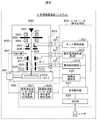
- the scanning electron beam measurement / inspection apparatus is based on the conventional measurement / inspection apparatus (system) using the scanning electron beam system shown in FIG.
- the configuration of the control circuit of the deflector is adopted. First, the system configuration of FIG. 8 will be described.
- a conventional measurement / inspection apparatus is mainly composed of a scanning electron microscope 800 and a computer 820.
- the scanning electron microscope 800 includes a lens barrel 830 and a sample chamber 840. Inside the lens barrel 830, an electron gun 801 that emits an electron beam A21 as an irradiation system (electron optical system), and an emitted electron beam A21. Focusing lens (first condenser lens) 802, aperture 803, focusing lens (second condenser lens) 804, blanking control electrode 805, aperture 806, deflection electrode 808, objective lens 809, and the like.
- the lens barrel 830 includes a detector 807 that detects secondary electrons A211 generated from the sample 810 by the irradiated electron beam A21 (A24) as a detection system. Further, an orthogonal electromagnetic field generator (ExB) 816 is provided as a means for separating the primary beam and the secondary beam.
- ExB orthogonal electromagnetic field generator
- the computer 820 includes an overall control unit 824, a blanking (BLK) control circuit 821, an orthogonal electromagnetic deflector (ExB) 822, a deflection control circuit 823, a mechanism system control unit 825, and a signal detection unit (secondary electron signal).
- Detection circuit 827, image processing unit (secondary electron signal processing circuit) 828, stage position detection unit (not shown), electron optical system control unit (not shown), GUI unit (user interface unit) 826, etc. Prepare.
- the electron beam A21 generated and emitted from the electron gun 801 is focused through a first condenser lens (focusing lens) 802, a diaphragm 803, and a second condenser lens (focusing lens) 804. Then, movement and scanning deflection control is performed to the irradiation center of the beam via the deflection electrode 808, and irradiation is performed while scanning the sample 810 through the objective lens 809 and the like.
- the beam A21 (A24) is irradiated, secondary electrons A211 are generated from the sample 810, and are incident on the detector 807 and detected by the deflection action of the orthogonal electromagnetic deflector (ExB) 822.
- the signal (analog signal) detected by the detector 807 is converted into a digital signal by a signal detection unit 827 (secondary electron signal detection circuit).
- a two-dimensional image is generated and processed by the image processing unit 828 (secondary electron signal processing circuit) based on the digital signal, and the processed result is displayed on the screen of the GUI unit 826.
- a circuit pattern is measured based on this image (in the case of a measurement function).
- the GUI unit 826 performs a process of providing an interface (such as a GUI screen) to a user (measurement / inspector).
- the GUI unit 826 provides a GUI screen for inputting (setting) inspection conditions and the like, a GUI screen for displaying inspection results (such as a two-dimensional image), and the like.
- the overall control unit 824 performs processing for controlling the entire system (apparatus) in accordance with an instruction from the GUI unit 826.
- An electron optical system control unit (not shown) controls the electron optical system (irradiation system) in the lens barrel 830 according to the control from the overall control unit 824.
- the mechanical system control unit 825 controls a mechanical system including a motor 841 that drives a sample stage 812 installed in the sample chamber 840.
- the rotation signal of the motor 841 is sent to a stage position detector (not shown), and position information of the sample stage (stage) 812 is obtained.
- a current control coil is used as a means for separating the primary beam and the secondary beam.
- An electromagnetic deflector (ExB) is employed in which the magnetic field generated in Fig. 4 and the electric field generated by voltage control are orthogonal to each other.
- the orthogonal electromagnetic deflector (ExB) 822 on the primary beam and the secondary beam will be described with reference to FIGS. 3, 4, and 5.
- the orthogonal electromagnetic deflector (ExB) is generally arranged in the X and Y directions as shown in FIG. 3 to deflect the secondary beam in an arbitrary direction. 4 and 5, only the electromagnetic deflector and the electric field deflector in the X direction and their respective control circuits are shown for simplification, and the Y direction is omitted.
- FIG. 4 is an overhead view of the orthogonal electromagnetic deflector and the secondary beam A211.
- FIG. 5 is an overhead view of the orthogonal electromagnetic deflector and the primary beam A21.
- Ve is a voltage between the electrodes of the electric field deflector
- Ke is a constant determined by the shape and arrangement of the electrode 816e and the counter electrode 816f.
- the secondary electrons (or reflected electrons) A211 generated from the sample 810 are deflected in the same direction, that is, the electrode side by the electric field and the magnetic field because the traveling direction is reverse to that of the primary electrons A21.
- the deflection angle depends on the energy of the secondary electrons (or reflected electrons) A211.
- K is a constant that determines the deflection angle of secondary electrons and reflected electrons.
- Vx Kx ⁇ Ix.
- This Win condition is a condition in which the electric field and magnetic field generated by the orthogonal electromagnetic deflector cancel the influence on the primary beam.
- Kx depends on the electrode shape and arrangement of the orthogonal electromagnetic deflector, the coil shape and arrangement, and the acceleration speed of the primary beam.
- the win condition is the relationship between the electric field control voltage and the magnetic field control current in the same direction.
- the amount of deflection is inversely proportional to the acceleration voltage Vacc due to the electric field, and the amount of deflection is inversely proportional to the route of the acceleration voltage Vacc due to the magnetic field. Therefore, adjustment of K1, K2, K3, and K4 is necessary according to the acceleration voltage Vacc of the primary beam.
- the conventional device is characterized in that the generation circuits are independent so that the relationship between the voltage value for controlling the electric field and the current value for controlling the magnetic field can be arbitrarily adjusted.
- circuit noise generated in the circuit constituent element causes a scanning position shift of the primary electron beam.
- the relationship between the noise of the control circuit of the orthogonal electromagnetic deflector and the scanning deviation of the primary electron beam will be described with reference to FIGS. 6 and 7, the X direction of the single-stage orthogonal electromagnetic deflector will be described.
- the multi-stage orthogonal electromagnetic deflector and the X direction are used. It is not limited to the configuration.
- the electron beam deflection amount Lex on the sample (wafer) is given by the following simplified formula (formula 3) if the primary electron beam deflection sensitivity is S_ex by an electric field.
- Vx K1 ⁇ Ix
- the deflection direction is reversed, and there is no scanning deviation of the primary electron beam.
- the noise 823e of the X-direction electric field control voltage is N_ECV_X
- the noise 823f of the electric field drive voltage source circuit is N_EAmpV_X
- the deviation of the primary electron beam due to these random noises The amount is (Expression 5):
- L_ENX (( N_ECV_X * GE1 + N_EAmpV_X * GE2) * S_ex It is expressed by the following formula.
- L _EXBNX (( N _ECV_X - N _BCV_X) ⁇ GB1 + (N _EAmpV_X - N _BCV_X) ⁇ GB2) ⁇ S_bx It is expressed by the following formula.
- the secondary electrons are deflected to the detector side by the electric field, and the influence of the electric field on the primary electron beam is canceled out.
- a configuration for generating a magnetic field in a direction orthogonal to the electric field so as to guide secondary electrons to the detector side will be described.
- the control signal generator of the voltage source circuit for controlling the electric field deflector and the current source control circuit for controlling the magnetic field deflector are shared. And a configuration for adjusting the voltage signal for controlling the electric field based on the current signal for controlling the magnetic field to satisfy the Win condition will be described.
- the scanning electron beam type measurement / inspection apparatus in the present embodiment includes an electric field deflector and a magnetic field deflector in the orthogonal electromagnetic deflector of the configuration of the conventional scanning electron beam type measurement / inspection apparatus described in FIG.
- the configuration of the control circuit of the orthogonal electromagnetic deflector to be controlled is replaced with the configuration as shown in FIG. Therefore, the following description will be made with reference to FIGS.
- the quadrature electromagnetic deflector In the quadrature electromagnetic deflector, secondary electrons and reflected electrons are deflected in the direction toward the detector. Therefore, in order to control the deflection in two orthogonal directions (X direction and Y direction) independently from each other, the minimum X , Y direction deflection electrodes and deflection coils are required.
- a 21 is a deflection voltage that is focused through the first condenser lens (focusing lens) 802, the stop 803, and the second condenser lens (focusing lens) 804 and travels through the electric field formed by the deflection electrode 808 and is applied to the deflection electrode 808. Accordingly, the electron beam is subjected to scanning deflection control and irradiated while scanning the sample 810 through the objective lens 809 and the like.
- Secondary electrons (or backscattered electrons) A211 generated from the sample 810 by irradiation of the primary electron beam A21 receive forces from the magnetic field deflectors 116a and 116b and the electric field deflectors 116e and 116f constituting the orthogonal electromagnetic deflector 816. Then, it is deflected in the direction of the detector 807 and detected.
- the deflection angle of the detected secondary beam (secondary electrons / reflected electrons) A211 is proportional to the strength of the electric field / magnetic field generated by the orthogonal electromagnetic deflector 816 and inversely proportional to the energy of the secondary beam A211.
- the magnitude of the electric field / magnetic field generated by the orthogonal electromagnetic deflector 816 is changed to a control circuit for the orthogonal electromagnetic deflector.
- the output voltage / output current 302 is controlled.
- the output voltage Vx of the voltage source circuit that controls the electric field and the output current of the current source circuit that controls the magnetic field are controlled so that the electric field / magnetic field generated by the orthogonal electromagnetic deflector 816 does not affect the scanning position of the primary electron beam A21. Ix satisfies the win condition.
- the control circuit 302 of the orthogonal electromagnetic deflector generates a voltage value 302a1 for determining the deflection angle of the secondary beam according to the energy of the secondary beam A211 from the electric field / magnetic field common voltage generator 302a.
- the generated voltage value is converted / amplified into a current for controlling the magnetic field by the magnetic field drive current source circuit 302c and applied to the magnetic deflectors 116a and 116b.
- the voltage value 302a1 is adjusted so that the output voltage Vx of the voltage source circuit for controlling the electric field by the gain adjusting unit 302b and the output current Ix of the current source circuit for controlling the magnetic field satisfy the WIN condition.
- the voltage is amplified to a voltage for controlling the electric field by the source circuit 302c and applied to the electric field deflectors 116e and 116f.
- the main part of the control circuit noise of the orthogonal electromagnetic deflector that causes the positional deviation of the primary electron beam A21 in the conventional apparatus configuration is an in-phase component common to the electric field control circuit and the magnetic field control circuit.
- the electric field and the magnetic field caused by the noise in this part are in opposite directions, and the magnitude satisfies the WIN condition.
- the frequency characteristics and phase characteristics of the voltage source control signal coincide with the frequency characteristics and phase characteristics of the current source control signal.
- the noise portion of the electric field deflector and the magnetic field deflector can be canceled, and the positional deviation of the primary electron beam can be reduced.
- the means for separating the primary and secondary electrons can be realized with a high voltage and a large current, and can be applied to the primary beam.
- the influence of shaking can be suppressed to the minimum, and the resolution and throughput can be improved.
- Example 2 of the present invention A scanning electron beam type measurement / inspection apparatus of Example 2 of the present invention and a measurement / inspection method using the same will be described with reference to FIG.
- FIG. 2 shows a case of a two-stage configuration.
- the feature of this two-stage secondary beam deflecting means is that the primary electron beam chromatic aberration problem can be solved by the one-stage secondary beam deflecting means.
- FIG. 2 shows the configuration of the entire system including the measurement / inspection apparatus according to the second embodiment.
- the measurement / inspection apparatus 1 according to the second embodiment is an application example that enables automatic measurement and inspection of a target semiconductor wafer (sample 110).
- the measurement and inspection apparatus 1 includes a measurement function for measuring a dimension value in a circuit pattern of a semiconductor wafer (sample 110) and an inspection function for detecting a defect (abnormality or defect) in the pattern.
- the measurement and inspection apparatus (system) 1 is mainly composed of a scanning electron microscope 100 and a signal processing / control computer 200.
- the scanning electron microscope 100 includes a column 150 and a sample chamber 130. Inside the sample chamber 130, a sample stage (stage) 112 on which a sample 110 that is an object of measurement / inspection is placed, and the sample stage Is installed.
- an electron gun 101 that emits an electron beam A1 and a focusing lens (first condenser lens) through which the emitted electron beam A1 passes.
- a focusing lens second condenser lens
- BLK blanking
- the column 150 serves as a detection system.
- the detector 107 detects secondary electrons / reflected electrons A11 generated from the sample 110 by the irradiated electron beam A1 (A4), and deflects A11 in the direction of the detector 107.
- a secondary electron / reflected electron orthogonal electromagnetic deflector 160 is provided.
- the deflector 170 is an orthogonal electromagnetic deflector that corrects chromatic aberration of the primary electron beam A1 (A4) generated by the deflector 160.
- electron beams A1 and A4 (not shown) correspond to A21 and A24 shown in FIG. 8, respectively.
- the computer 200 is configured to be stored in a control rack in the form of a PC or a control board, for example.
- Each unit of the computer 200 is realized by, for example, software program processing using a processor and a memory, or processing of a dedicated circuit.
- the computer 200 includes an overall control unit 210, a blanking (BLK) control circuit 201, an image shift / deflection control circuit 206 that controls position shift and deflection scanning of the electron beam, a mechanical system control unit 230, a signal A detection unit (secondary electron signal detection circuit) 207, an image processing unit (secondary electron signal processing circuit) 208, a GUI unit (user interface unit) 250, and the like are provided.
- BLK blanking
- image shift / deflection control circuit 206 that controls position shift and deflection scanning of the electron beam
- a mechanical system control unit 230 controls a mechanical system control unit 230
- signal A detection unit secondary electron signal detection circuit
- an image processing unit secondary electron signal processing circuit
- GUI unit user interface unit
- the electron beam A1 generated and emitted from the electron gun 101 is a first condenser lens (focusing lens) 102, a diaphragm 103, and a second condenser lens (focusing lens) 104.
- focusing lens a first condenser lens
- focusing lens a diaphragm 103
- second condenser lens focusing lens
- the deflector 120 that is focused through and integrated with image shift and scanning, movement and scanning deflection are controlled at the irradiation center of the beam, and irradiation is performed while scanning the sample 110 through the objective lens 109 and the like.
- the beam A1 (A4) is irradiated, secondary electrons A11 are generated from the sample 110 and detected by the detector 107.
- a signal (analog signal) detected by the detector 107 is converted into a digital signal by a signal detection unit 207 (secondary electron signal detection circuit).
- a two-dimensional image is generated and displayed on the GUI screen by the image processing unit 208 (secondary electron signal processing circuit) based on the digital signal.
- a circuit pattern is measured based on this image (in the case of a measurement function).
- the GUI unit 250 performs a process of providing an interface (such as a GUI screen) to a user (measurement / inspector).
- the GUI unit 250 provides a GUI screen for inputting (setting) inspection conditions and the like, a GUI screen for displaying inspection results (such as a two-dimensional image), and the like.
- the GUI unit 250 includes an input / output device such as a keyboard and a display, a communication interface unit, and the like. The user can select and execute a measurement function and an inspection function on the GUI screen.
- the overall control unit 210 is configured according to an instruction from the GUI unit 250 (the electronic optical control unit 220, the mechanical system control unit 230, the image shift / deflection control circuit 206, the signal detection unit 207, the image processing unit). 208, a stage position detection unit, etc.) is controlled.
- the overall control unit 210 includes the electro-optic control unit 220, the image shift / deflection control circuit 206, the mechanical system control unit 230, and the like according to measurement / inspection conditions and instructions input by the user on the screen of the GUI unit 250.
- the measurement process is performed.
- the overall control unit 210 receives data information such as a two-dimensional image generated through the signal processing unit 207 and the image processing unit 208 and displays the data information on the screen of the GUI unit 250.
- the electron optical control unit 220 controls the electron gun 101 in the column 100, the first condenser lens (focusing lens) 102, the diaphragm 103, the second condenser lens (focusing lens) 104, and blanking control in accordance with the control from the overall control unit 210.
- the electron optical system irradiation system
- the blanking control circuit 201 controls the blanking control electrode 105 via the signal line to stop the irradiation of the electron beam A1 to the sample 110, the trajectory of the electron beam A1 is bent and the electron beam A1 is made to be the aperture 106. To irradiate.
- the image shift / deflection control circuit 206 shifts the position of the electron beam by applying a deflection control signal to the deflector 120 through the signal lines (c1, c2) according to the control from the overall control unit 210. Controls scanning by deflection at the shifted position.
- the control unit of the two-stage orthogonal electromagnetic deflector 303 sends a secondary beam deflection control signal to the orthogonal electromagnetic deflector 160 that separates the primary beam and the secondary beam through the signal line (b1) in accordance with the control from the overall control unit 210.
- a secondary beam deflection control signal to the orthogonal electromagnetic deflector 160 that separates the primary beam and the secondary beam through the signal line (b1) in accordance with the control from the overall control unit 210.
- the two-stage orthogonal electromagnetic deflector control unit 303 applies orthogonality by applying a primary electron beam chromatic aberration correction control signal to the orthogonal electromagnetic deflector 170 through the signal line (b2) in accordance with the control from the overall control unit 210.
- the electromagnetic deflector 160 largely controls the correction of the chromatic aberration of the primary electron beam caused by largely deflecting the secondary beam by generating a reverse electric field and a magnetic field.
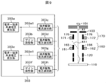
- FIG. 9 is a block diagram showing the configuration of a two-stage orthogonal electromagnetic deflector 303 and its control circuit according to Embodiment 2 of the present invention. As shown in FIG. 9, it comprises a part for controlling the upper deflector 170 and a part for controlling the lower deflector 160 of the two-stage orthogonal electromagnetic deflector.
- the configuration of each stage control circuit is the same as that described in the first embodiment, and the signal generation unit of the voltage source circuit and the current source circuit is shared.
- the frequency characteristics and phase characteristics of the voltage source control signal and the current source control signal are matched. Therefore, the electric field deflector and the magnetic field deflector can be canceled out with respect to the deflecting force to the primary electron beam caused by the common circuit noise of each stage electromagnetic deflector control circuit, and the displacement of the primary electron beam can be reduced.
- a common control can be performed by providing a filter in each output stage so that the frequency band and attenuation characteristics of the voltage source circuit and current source circuit are the same.
- the phase / frequency characteristics of noise generated in the signal section can be matched.
- the mechanism system control unit 230 controls the mechanism system including the motor 131 and the like that drives the sample stage 112 installed in the sample chamber 130. For example, it is possible to control the movement of the sample stage 112 by driving the motor 131 in accordance with the scanning control of the electron beam. At this time, the rotation signal of the motor 131 is sent to a stage position detector (not shown), and position information of the sample stage 112 is obtained.
- the image processing unit 208 generates a measurement image at the time of measurement (measurement function), calculates a pattern dimension value in the image, and the inspection image at the time of inspection (inspection function). A process for generating and detecting / determining defects in the image is performed.
- a two-stage configuration as a primary beam / secondary beam separation means in order to improve throughput and measurement accuracy.
- the orthogonal electromagnetic deflector is used.
- the high voltage and large current of the means for separating the primary and secondary electrons can be realized, and the influence and aberration on the primary beam can be suppressed to the minimum, and the resolution and throughput can be improved.
- the configuration described in the first embodiment only the X direction (or Y direction) of the orthogonal electromagnetic deflector is shown.
- the configuration of the scanning electron beam measurement / inspection apparatus in this embodiment is similar to that of the orthogonal electromagnetic deflector and the control. Circuits are provided in both X and Y directions.
- FIG. 10 is a block diagram showing the configuration of the control circuit of the orthogonal electromagnetic deflector according to the third embodiment of the present invention.
- the control circuit for the orthogonal electromagnetic deflector described in the first embodiment is composed of a voltage source circuit and a current source circuit for controlling the electric field and magnetic field of the orthogonal electromagnetic deflection in both the X and Y directions.
- the signal generator of the voltage source circuit and the current source circuit is shared in order to minimize the influence of the position shift on the primary electron beam.
- the frequency characteristic and phase characteristic of the voltage source control signal are matched with the frequency characteristic and phase characteristic of the current source control signal. Therefore, the electric field deflector and magnetic field deflector can cancel out the deflection force to the primary electron beam caused by the common circuit noise of the orthogonal electromagnetic deflector control circuit for each direction, and the displacement of the primary electron beam is reduced. it can.
- X, Y can be used as primary beam / secondary beam separation means.
- Each of the directions is composed of orthogonal electromagnetic deflectors.
- the high voltage and large current of the means for separating the primary and secondary electrons can be realized, and the influence and aberration on the primary beam can be suppressed to the minimum, and the resolution and throughput can be improved.
- the orthogonal electromagnetic deflector and the control circuit are provided in both the X and Y directions.
- the control voltage and control current in each direction are controlled independently.
- the orthogonal electromagnetic deflector and the control circuit are provided in both the X and Y directions.
- the control voltage and the control current in both X and Y directions are not independent. This is because the electromagnetic fields generated independently in the X and Y directions are not orthogonal to each other due to manufacturing and mounting errors of the X direction electrodes, coils and Y direction electrodes, and coils, so it is necessary to correct the rotation effect. is there.
- FIG. 11 is a block diagram showing the configuration of the control circuit of the orthogonal electromagnetic deflector according to the fourth embodiment of the present invention.
- the control circuit of the orthogonal electromagnetic deflector includes a voltage source circuit and a current source circuit that control the electric field and magnetic field of the orthogonal electromagnetic deflector in both the X and Y directions.
- the orthogonal electromagnetic deflector control circuit 305 includes an X-direction orthogonal electromagnetic deflector control unit and a Y-direction electric field / magnetic field orthogonal electromagnetic deflector control unit.
- the X-direction orthogonal electromagnetic deflector control unit generates a voltage value 305a1 for determining the X-direction deflection angle of the secondary beam according to the energy of the secondary beam from the X-direction electric field / magnetic field common voltage generation unit 305a.
- the Y-direction orthogonal electromagnetic deflector control unit generates a voltage value 305d1 for determining the Y-direction deflection angle of the secondary beam according to the energy of the secondary beam from the Y-direction electric field / magnetic field common voltage generation unit 305d.
- the generated X-direction common voltage value 305a1 is converted / amplified into a current for controlling the X-direction magnetic field by the X-direction magnetic field drive current source circuit 305b, and applied to the X-direction magnetic deflector.
- the generated Y-direction common voltage value 305d1 is converted and amplified to a current for controlling the Y-direction magnetic field by the Y-direction magnetic field drive current source circuit 305e, and applied to the Y-direction magnetic deflector.
- the output voltage Vx of the voltage source circuit that controls the X-direction electric field has an X-direction common voltage value 305a1 and a Y-direction common voltage value 305d1, respectively.
- the adjustment results of the gain adjusting means 305g and 305h are added, and the value is input to the electric field driving voltage source circuit 305c, amplified to a voltage for controlling the electric field by the electric field driving voltage source circuit 305c, and applied to the X-direction electric field deflector. To do.
- the output voltage Vy of the voltage source circuit that controls the Y-direction electric field has an X-direction common voltage value 305a1 and a Y-direction common voltage value 305d1, respectively.
- the adjustment results of the gain adjusting means 305i and 305j are added, and the value is input to the electric field drive voltage source circuit 305f, amplified to a voltage for controlling the electric field by the electric field drive voltage source circuit 305f, and sent to the Y-direction electric field deflector.
- the main part of the electromagnetic deflector control circuit noise that causes the positional deviation of the primary electron beam is compared to the electric field control circuit and the magnetic field control circuit. Therefore, the electric field and magnetic field fluctuation directions caused by the noise in this part are opposite directions, and the magnitude satisfies the WIN condition. Further, the frequency characteristic and phase characteristic of the voltage source control signal are matched with the frequency characteristic and phase characteristic of the current source control signal.
- X, Y can be used as primary beam / secondary beam separation means.
- An orthogonal electromagnetic deflector capable of correcting the rotational effect of the directional electromagnetic deflector is used.
- the high voltage and large current of the means for separating the primary and secondary electrons can be realized, and the influence and aberration on the primary beam can be suppressed to the minimum, and the resolution and throughput can be improved.
- the main features of the charged particle beam apparatus of the present invention having the above-described configuration are as follows.
- a charged particle gun for generating a charged particle beam
- An electron optical system that irradiates and scans a sample placed on a stage with a charged particle beam emitted from the charged particle gun; and
- a detection unit for detecting secondary electrons generated from the sample or reflected electrons
- An orthogonal electromagnetic deflection unit that deflects the path of the secondary electrons or reflected electrons in the direction of the detection unit, and
- the orthogonal electromagnetic deflection unit includes a magnetic field deflector that generates a magnetic field to change a locus of the charged particle beam, an electric field deflector that generates an electric field to change the locus of the charged particle beam, and the magnetic field deflector.
- a current source circuit for supplying a current, a voltage source circuit for supplying a voltage to the electric field deflector, and a gain adjusting unit for adjusting a relationship between the current and the voltage The magnetic field deflector and the electric field deflector are arranged so that the magnetic field and the electric field are perpendicular to each other and overlap each other, A voltage generator that applies a voltage to the current source circuit and a voltage generator that applies a voltage to the voltage source circuit are shared in one, The gain adjustment unit adjusts the relationship between the current and the voltage so that the amount by which the path is deflected by the magnetic field matches the amount by which the path is deflected by the electric field.
- a charged particle beam device characterized by that.
- a charged particle gun that generates a charged particle beam
- An electron optical system that irradiates and scans a sample placed on a stage with a charged particle beam emitted from the charged particle gun; and A detection unit for detecting secondary electrons generated from the sample or reflected electrons;
- An orthogonal electromagnetic deflection unit that deflects the path of the secondary electrons or reflected electrons in the direction of the detection unit, and
- the orthogonal electromagnetic deflection unit includes a first electric field deflector and a first magnetic field deflector that apply an electric field and a magnetic field, respectively, in a first direction intersecting a path direction of a charged particle beam emitted from the charged particle gun.
- a second electric field deflector and a second magnetic field deflector for applying an electric field and a magnetic field in a second direction orthogonal to the first direction, and the first and second magnetic field deflectors, respectively.
- First and second current source circuits for supplying a current
- first and second voltage source circuits for supplying a voltage to each of the first and second electric field deflectors, and the current and the voltage
- a first and a second gain adjustment unit for adjusting the relationship, respectively.
- the first and second magnetic field deflectors generate a magnetic field to change a trajectory of the charged particle beam
- the first and second electric field deflectors generate an electric field to generate a trajectory of the charged particle beam.
- the first and second magnetic field deflectors and the first and second electric field deflectors are arranged so that respective magnetic fields and electric fields are perpendicular to each other and overlap each other, A voltage generator that applies a voltage to the first current source circuit and a voltage generator that applies a voltage to the first voltage source circuit; A voltage generator that applies a voltage to the second voltage source circuit, and a voltage generator that applies a voltage to the second voltage source circuit; Have The first voltage generation unit and the second voltage generation unit control the voltage independently of each other, The amount by which the path of the magnetic field is deflected by the first magnetic field deflector and the amount by which the path is deflected by the electric field of the first electric field deflector are matched by the first gain adjusting unit.
- the relationship between the current and the voltage is adjusted, The amount by which the path of the magnetic field is deflected by the second magnetic field deflector and the amount by which the path is deflected by the electric field of the second field deflector are matched by the second gain adjusting unit.
- the relationship between the current and the voltage is adjusted, A charged particle beam device characterized by that.
- Measurement inspection device 100: Scanning electron microscope (column), 101 ... an electron gun, 102 ... 1st condenser lens (focusing lens), 103 ... Aperture, 104 ... Second condenser lens (focusing lens), 105 ... Blanking (BLK) control electrode, 106 ... Aperture, 107 ... Detector (secondary electron / reflected electron detector), 109 ... objective lens, 110 ... Sample, 112 ... Sample stage (stage), 120 ... deflector, 160 ... Orthogonal electromagnetic deflector, 200: Computer (signal processing system), 201 ... Blanking (BLK) control circuit, 206: Image shift / deflection control circuit, 207 ...
- Signal detection unit (secondary electron signal detection circuit), 208: Image processing unit (secondary electron signal processing circuit), 210 ... Overall control unit, 220: Electro-optical control unit, 230 ... mechanical system control unit, 250 ... GUI part, 303 ... Orthogonal electromagnetic deflector, 302: Control circuit for orthogonal electromagnetic deflector.
Landscapes
- Chemical & Material Sciences (AREA)
- Analytical Chemistry (AREA)
- Testing Or Measuring Of Semiconductors Or The Like (AREA)
Priority Applications (2)
| Application Number | Priority Date | Filing Date | Title |
|---|---|---|---|
| US15/109,230 US9679740B2 (en) | 2014-01-09 | 2014-12-16 | Charged particle beam device |
| US15/613,941 US10424459B2 (en) | 2014-01-09 | 2017-06-05 | Charged particle beam device |
Applications Claiming Priority (2)
| Application Number | Priority Date | Filing Date | Title |
|---|---|---|---|
| JP2014002260A JP6254445B2 (ja) | 2014-01-09 | 2014-01-09 | 荷電粒子ビーム装置 |
| JP2014-002260 | 2014-02-04 |
Related Child Applications (2)
| Application Number | Title | Priority Date | Filing Date |
|---|---|---|---|
| US15/109,230 A-371-Of-International US9679740B2 (en) | 2014-01-09 | 2014-12-16 | Charged particle beam device |
| US15/613,941 Continuation US10424459B2 (en) | 2014-01-09 | 2017-06-05 | Charged particle beam device |
Publications (1)
| Publication Number | Publication Date |
|---|---|
| WO2015104959A1 true WO2015104959A1 (ja) | 2015-07-16 |
Family
ID=53523797
Family Applications (1)
| Application Number | Title | Priority Date | Filing Date |
|---|---|---|---|
| PCT/JP2014/083200 Ceased WO2015104959A1 (ja) | 2014-01-09 | 2014-12-16 | 荷電粒子ビーム装置 |
Country Status (3)
| Country | Link |
|---|---|
| US (2) | US9679740B2 (enExample) |
| JP (1) | JP6254445B2 (enExample) |
| WO (1) | WO2015104959A1 (enExample) |
Cited By (1)
| Publication number | Priority date | Publication date | Assignee | Title |
|---|---|---|---|---|
| TWI703607B (zh) * | 2018-03-30 | 2020-09-01 | 日商日立全球先端科技股份有限公司 | 荷電粒子束應用裝置 |
Families Citing this family (10)
| Publication number | Priority date | Publication date | Assignee | Title |
|---|---|---|---|---|
| JP6254445B2 (ja) * | 2014-01-09 | 2017-12-27 | 株式会社日立ハイテクノロジーズ | 荷電粒子ビーム装置 |
| WO2016016957A1 (ja) * | 2014-07-30 | 2016-02-04 | 株式会社 日立ハイテクノロジーズ | パターン高さ測定装置、及び荷電粒子線装置 |
| US10090131B2 (en) * | 2016-12-07 | 2018-10-02 | Kla-Tencor Corporation | Method and system for aberration correction in an electron beam system |
| CN111033677B (zh) * | 2017-09-04 | 2022-08-23 | 株式会社日立高新技术 | 带电粒子线装置 |
| WO2020078660A1 (en) * | 2018-10-19 | 2020-04-23 | Asml Netherlands B.V. | System and method for aligning electron beams in multi-beam inspection apparatus |
| WO2020183551A1 (ja) * | 2019-03-08 | 2020-09-17 | 株式会社日立ハイテク | 荷電粒子ビーム装置 |
| JP2021197263A (ja) * | 2020-06-12 | 2021-12-27 | 株式会社ニューフレアテクノロジー | マルチ電子ビーム画像取得装置及びマルチ電子ビーム画像取得方法 |
| CN112071732B (zh) * | 2020-07-28 | 2021-11-19 | 西安交通大学 | 一种可编码阵列式静电偏转器、聚焦偏转系统及设计方法 |
| EP4086934A1 (en) * | 2021-05-04 | 2022-11-09 | ASML Netherlands B.V. | Electron optical column and method for directing a beam of primary electrons onto a sample |
| EP4268257A1 (en) * | 2020-12-22 | 2023-11-01 | ASML Netherlands B.V. | Electron optical column and method for directing a beam of primary electrons onto a sample |
Citations (3)
| Publication number | Priority date | Publication date | Assignee | Title |
|---|---|---|---|---|
| JPH0260042A (ja) * | 1988-08-24 | 1990-02-28 | Hitachi Ltd | 荷電粒子線応用装置の駆動電源 |
| JPH02142045A (ja) * | 1988-11-24 | 1990-05-31 | Hitachi Ltd | 荷電粒子線応用装置 |
| JP2006332038A (ja) * | 2005-04-28 | 2006-12-07 | Hitachi High-Technologies Corp | 荷電粒子ビームを用いた検査方法及び検査装置 |
Family Cites Families (8)
| Publication number | Priority date | Publication date | Assignee | Title |
|---|---|---|---|---|
| JP3867048B2 (ja) * | 2003-01-08 | 2007-01-10 | 株式会社日立ハイテクノロジーズ | モノクロメータ及びそれを用いた走査電子顕微鏡 |
| US7462828B2 (en) | 2005-04-28 | 2008-12-09 | Hitachi High-Technologies Corporation | Inspection method and inspection system using charged particle beam |
| JP4988216B2 (ja) | 2006-02-03 | 2012-08-01 | 株式会社日立ハイテクノロジーズ | 収差補正装置を搭載した荷電粒子線装置 |
| JP2008181786A (ja) | 2007-01-25 | 2008-08-07 | Hitachi High-Technologies Corp | 荷電粒子線装置 |
| EP2132763B1 (en) | 2007-02-22 | 2014-05-07 | Applied Materials Israel Ltd. | High throughput sem tool |
| JP4977509B2 (ja) * | 2007-03-26 | 2012-07-18 | 株式会社日立ハイテクノロジーズ | 走査電子顕微鏡 |
| JP5237734B2 (ja) | 2008-09-24 | 2013-07-17 | 日本電子株式会社 | 収差補正装置および該収差補正装置を備える荷電粒子線装置 |
| JP6254445B2 (ja) * | 2014-01-09 | 2017-12-27 | 株式会社日立ハイテクノロジーズ | 荷電粒子ビーム装置 |
-
2014
- 2014-01-09 JP JP2014002260A patent/JP6254445B2/ja active Active
- 2014-12-16 US US15/109,230 patent/US9679740B2/en active Active
- 2014-12-16 WO PCT/JP2014/083200 patent/WO2015104959A1/ja not_active Ceased
-
2017
- 2017-06-05 US US15/613,941 patent/US10424459B2/en active Active
Patent Citations (3)
| Publication number | Priority date | Publication date | Assignee | Title |
|---|---|---|---|---|
| JPH0260042A (ja) * | 1988-08-24 | 1990-02-28 | Hitachi Ltd | 荷電粒子線応用装置の駆動電源 |
| JPH02142045A (ja) * | 1988-11-24 | 1990-05-31 | Hitachi Ltd | 荷電粒子線応用装置 |
| JP2006332038A (ja) * | 2005-04-28 | 2006-12-07 | Hitachi High-Technologies Corp | 荷電粒子ビームを用いた検査方法及び検査装置 |
Cited By (1)
| Publication number | Priority date | Publication date | Assignee | Title |
|---|---|---|---|---|
| TWI703607B (zh) * | 2018-03-30 | 2020-09-01 | 日商日立全球先端科技股份有限公司 | 荷電粒子束應用裝置 |
Also Published As
| Publication number | Publication date |
|---|---|
| US20170271121A1 (en) | 2017-09-21 |
| US9679740B2 (en) | 2017-06-13 |
| US10424459B2 (en) | 2019-09-24 |
| US20160329186A1 (en) | 2016-11-10 |
| JP6254445B2 (ja) | 2017-12-27 |
| JP2015130309A (ja) | 2015-07-16 |
Similar Documents
| Publication | Publication Date | Title |
|---|---|---|
| JP6254445B2 (ja) | 荷電粒子ビーム装置 | |
| JP6155137B2 (ja) | 走査型電子顕微鏡を用いた処理装置及び処理方法 | |
| JP6408116B2 (ja) | 荷電粒子ビーム装置 | |
| JP6677519B2 (ja) | 電子顕微鏡および収差測定方法 | |
| US9230775B2 (en) | Charged particle instrument | |
| US20150357153A1 (en) | Charged particle beam device | |
| US9704687B2 (en) | Charged particle beam application device | |
| JP5927067B2 (ja) | 計測検査装置、及び計測検査方法 | |
| US11430630B2 (en) | Charged particle beam apparatus | |
| US9960006B2 (en) | Charged-particle-beam device | |
| US8735814B2 (en) | Electron beam device | |
| US20120119087A1 (en) | Charged-particle microscope | |
| JP5972663B2 (ja) | 電子ビーム応用装置および電子ビーム調整方法 | |
| TWI753374B (zh) | 荷電粒子束裝置 | |
| JP4273141B2 (ja) | 集束イオンビーム装置 | |
| JP2008084823A (ja) | 荷電粒子線調整方法及び荷電粒子線装置 | |
| US6717144B2 (en) | Scanning electron microscope system | |
| JP6563576B2 (ja) | 荷電粒子ビーム装置 | |
| US7060985B2 (en) | Multipole field-producing apparatus in charged-particle optical system and aberration corrector | |
| JP6282076B2 (ja) | 荷電粒子線装置 | |
| JP4431624B2 (ja) | 荷電粒子線調整方法、及び荷電粒子線装置 | |
| US20250239430A1 (en) | Charged particle beam device | |
| JPWO2019021455A1 (ja) | 収差補正装置及び荷電粒子線装置 | |
| JP2020074294A (ja) | 荷電粒子線装置 |
Legal Events
| Date | Code | Title | Description |
|---|---|---|---|
| 121 | Ep: the epo has been informed by wipo that ep was designated in this application |
Ref document number: 14877778 Country of ref document: EP Kind code of ref document: A1 |
|
| WWE | Wipo information: entry into national phase |
Ref document number: 15109230 Country of ref document: US |
|
| NENP | Non-entry into the national phase |
Ref country code: DE |
|
| 122 | Ep: pct application non-entry in european phase |
Ref document number: 14877778 Country of ref document: EP Kind code of ref document: A1 |